EP2071425A1 - Circuit installation capable of full voltage activation, division voltage operation and delayed breaking - Google Patents
Circuit installation capable of full voltage activation, division voltage operation and delayed breaking Download PDFInfo
- Publication number
- EP2071425A1 EP2071425A1 EP07254872A EP07254872A EP2071425A1 EP 2071425 A1 EP2071425 A1 EP 2071425A1 EP 07254872 A EP07254872 A EP 07254872A EP 07254872 A EP07254872 A EP 07254872A EP 2071425 A1 EP2071425 A1 EP 2071425A1
- Authority
- EP
- European Patent Office
- Prior art keywords
- impedance
- voltage
- capacitor
- series
- resistance
- Prior art date
- Legal status (The legal status is an assumption and is not a legal conclusion. Google has not performed a legal analysis and makes no representation as to the accuracy of the status listed.)
- Granted
Links
Images


Classifications
-
- H—ELECTRICITY
- H01—ELECTRIC ELEMENTS
- H01H—ELECTRIC SWITCHES; RELAYS; SELECTORS; EMERGENCY PROTECTIVE DEVICES
- H01H47/00—Circuit arrangements not adapted to a particular application of the relay and designed to obtain desired operating characteristics or to provide energising current
- H01H47/02—Circuit arrangements not adapted to a particular application of the relay and designed to obtain desired operating characteristics or to provide energising current for modifying the operation of the relay
- H01H47/18—Circuit arrangements not adapted to a particular application of the relay and designed to obtain desired operating characteristics or to provide energising current for modifying the operation of the relay for introducing delay in the operation of the relay
-
- H—ELECTRICITY
- H02—GENERATION; CONVERSION OR DISTRIBUTION OF ELECTRIC POWER
- H02M—APPARATUS FOR CONVERSION BETWEEN AC AND AC, BETWEEN AC AND DC, OR BETWEEN DC AND DC, AND FOR USE WITH MAINS OR SIMILAR POWER SUPPLY SYSTEMS; CONVERSION OF DC OR AC INPUT POWER INTO SURGE OUTPUT POWER; CONTROL OR REGULATION THEREOF
- H02M1/00—Details of apparatus for conversion
- H02M1/16—Means for providing current step on switching, e.g. with saturable reactor
-
- H—ELECTRICITY
- H02—GENERATION; CONVERSION OR DISTRIBUTION OF ELECTRIC POWER
- H02J—ELECTRIC POWER NETWORKS; CIRCUIT ARRANGEMENTS OR SYSTEMS FOR SUPPLYING OR DISTRIBUTING ELECTRIC POWER; SYSTEMS FOR STORING ELECTRIC ENERGY
- H02J7/00—Circuit arrangements for charging or discharging batteries or for supplying loads from batteries
- H02J7/34—Parallel operation in networks using both storage and other DC sources, e.g. providing buffering
- H02J7/345—Parallel operation in networks using both storage and other DC sources, e.g. providing buffering using capacitors as storage or buffering devices
-
- H—ELECTRICITY
- H02—GENERATION; CONVERSION OR DISTRIBUTION OF ELECTRIC POWER
- H02J—ELECTRIC POWER NETWORKS; CIRCUIT ARRANGEMENTS OR SYSTEMS FOR SUPPLYING OR DISTRIBUTING ELECTRIC POWER; SYSTEMS FOR STORING ELECTRIC ENERGY
- H02J7/00—Circuit arrangements for charging or discharging batteries or for supplying loads from batteries
- H02J7/865—Battery or charger load switching, e.g. concurrent charging and load supply
-
- H—ELECTRICITY
- H02—GENERATION; CONVERSION OR DISTRIBUTION OF ELECTRIC POWER
- H02J—ELECTRIC POWER NETWORKS; CIRCUIT ARRANGEMENTS OR SYSTEMS FOR SUPPLYING OR DISTRIBUTING ELECTRIC POWER; SYSTEMS FOR STORING ELECTRIC ENERGY
- H02J9/00—Circuit arrangements for emergency or stand-by power supply, e.g. for emergency lighting
- H02J9/005—Circuit arrangements for emergency or stand-by power supply, e.g. for emergency lighting using a power saving mode
-
- H—ELECTRICITY
- H02—GENERATION; CONVERSION OR DISTRIBUTION OF ELECTRIC POWER
- H02M—APPARATUS FOR CONVERSION BETWEEN AC AND AC, BETWEEN AC AND DC, OR BETWEEN DC AND DC, AND FOR USE WITH MAINS OR SIMILAR POWER SUPPLY SYSTEMS; CONVERSION OF DC OR AC INPUT POWER INTO SURGE OUTPUT POWER; CONTROL OR REGULATION THEREOF
- H02M3/00—Conversion of DC power input into DC power output
- H02M3/02—Conversion of DC power input into DC power output without intermediate conversion into AC
- H02M3/04—Conversion of DC power input into DC power output without intermediate conversion into AC by static converters
- H02M3/06—Conversion of DC power input into DC power output without intermediate conversion into AC by static converters using resistors or capacitors, e.g. potential divider
- H02M3/07—Conversion of DC power input into DC power output without intermediate conversion into AC by static converters using resistors or capacitors, e.g. potential divider using capacitors charged and discharged alternately by semiconductor devices with control electrode, e.g. charge pumps
-
- H—ELECTRICITY
- H02—GENERATION; CONVERSION OR DISTRIBUTION OF ELECTRIC POWER
- H02M—APPARATUS FOR CONVERSION BETWEEN AC AND AC, BETWEEN AC AND DC, OR BETWEEN DC AND DC, AND FOR USE WITH MAINS OR SIMILAR POWER SUPPLY SYSTEMS; CONVERSION OF DC OR AC INPUT POWER INTO SURGE OUTPUT POWER; CONTROL OR REGULATION THEREOF
- H02M7/00—Conversion of AC power input into DC power output; Conversion of DC power input into AC power output
- H02M7/02—Conversion of AC power input into DC power output without possibility of reversal
- H02M7/04—Conversion of AC power input into DC power output without possibility of reversal by static converters
- H02M7/12—Conversion of AC power input into DC power output without possibility of reversal by static converters using discharge tubes with control electrode or semiconductor devices with control electrode
- H02M7/145—Conversion of AC power input into DC power output without possibility of reversal by static converters using discharge tubes with control electrode or semiconductor devices with control electrode using devices of a thyratron or thyristor type requiring extinguishing means
- H02M7/155—Conversion of AC power input into DC power output without possibility of reversal by static converters using discharge tubes with control electrode or semiconductor devices with control electrode using devices of a thyratron or thyristor type requiring extinguishing means using semiconductor devices only
-
- H—ELECTRICITY
- H02—GENERATION; CONVERSION OR DISTRIBUTION OF ELECTRIC POWER
- H02M—APPARATUS FOR CONVERSION BETWEEN AC AND AC, BETWEEN AC AND DC, OR BETWEEN DC AND DC, AND FOR USE WITH MAINS OR SIMILAR POWER SUPPLY SYSTEMS; CONVERSION OF DC OR AC INPUT POWER INTO SURGE OUTPUT POWER; CONTROL OR REGULATION THEREOF
- H02M7/00—Conversion of AC power input into DC power output; Conversion of DC power input into AC power output
- H02M7/02—Conversion of AC power input into DC power output without possibility of reversal
- H02M7/04—Conversion of AC power input into DC power output without possibility of reversal by static converters
- H02M7/12—Conversion of AC power input into DC power output without possibility of reversal by static converters using discharge tubes with control electrode or semiconductor devices with control electrode
- H02M7/21—Conversion of AC power input into DC power output without possibility of reversal by static converters using discharge tubes with control electrode or semiconductor devices with control electrode using devices of a triode or transistor type requiring continuous application of a control signal
- H02M7/217—Conversion of AC power input into DC power output without possibility of reversal by static converters using discharge tubes with control electrode or semiconductor devices with control electrode using devices of a triode or transistor type requiring continuous application of a control signal using semiconductor devices only
-
- H—ELECTRICITY
- H03—ELECTRONIC CIRCUITRY
- H03K—PULSE TECHNIQUE
- H03K17/00—Electronic switching or gating, i.e. not by contact-making and –breaking
- H03K17/16—Modifications for eliminating interference voltages or currents
- H03K17/161—Modifications for eliminating interference voltages or currents in field-effect transistor switches
- H03K17/162—Modifications for eliminating interference voltages or currents in field-effect transistor switches without feedback from the output circuit to the control circuit
-
- H—ELECTRICITY
- H02—GENERATION; CONVERSION OR DISTRIBUTION OF ELECTRIC POWER
- H02M—APPARATUS FOR CONVERSION BETWEEN AC AND AC, BETWEEN AC AND DC, OR BETWEEN DC AND DC, AND FOR USE WITH MAINS OR SIMILAR POWER SUPPLY SYSTEMS; CONVERSION OF DC OR AC INPUT POWER INTO SURGE OUTPUT POWER; CONTROL OR REGULATION THEREOF
- H02M1/00—Details of apparatus for conversion
- H02M1/0083—Converters characterised by their input or output configuration
- H02M1/009—Converters characterised by their input or output configuration having two or more independently controlled outputs
-
- H—ELECTRICITY
- H02—GENERATION; CONVERSION OR DISTRIBUTION OF ELECTRIC POWER
- H02M—APPARATUS FOR CONVERSION BETWEEN AC AND AC, BETWEEN AC AND DC, OR BETWEEN DC AND DC, AND FOR USE WITH MAINS OR SIMILAR POWER SUPPLY SYSTEMS; CONVERSION OF DC OR AC INPUT POWER INTO SURGE OUTPUT POWER; CONTROL OR REGULATION THEREOF
- H02M3/00—Conversion of DC power input into DC power output
- H02M3/02—Conversion of DC power input into DC power output without intermediate conversion into AC
- H02M3/04—Conversion of DC power input into DC power output without intermediate conversion into AC by static converters
- H02M3/06—Conversion of DC power input into DC power output without intermediate conversion into AC by static converters using resistors or capacitors, e.g. potential divider
- H02M3/07—Conversion of DC power input into DC power output without intermediate conversion into AC by static converters using resistors or capacitors, e.g. potential divider using capacitors charged and discharged alternately by semiconductor devices with control electrode, e.g. charge pumps
- H02M3/072—Conversion of DC power input into DC power output without intermediate conversion into AC by static converters using resistors or capacitors, e.g. potential divider using capacitors charged and discharged alternately by semiconductor devices with control electrode, e.g. charge pumps adapted to generate an output voltage whose value is lower than the input voltage
Definitions
- the present invention is related to a circuit installation, and more particularly, to one that controls a power load taking advantage of charging, discharging and division voltage features of capacitor to provide activation and operation features different from those provided by a conventional ON-OFF switch.
- the pattern of control and operation of an electric load by conventional power switches usually involves ON or OFF only without the capacity to change the input voltage to the load.
- the primary purpose of the present invention is to provide a circuit installation that is capable of full voltage activation, division voltage operation and delayed breaking.
- the present invention by taking advantage of the features of a capacitor that integral boosting voltage in charging and differential dropping voltage in discharging connects the capacitor in series with an electric load; two sets of the said capacitor connected in series and the device of electric load are then connected in series in opposite sequence before being connected in parallel; and a diode is connected in series in positive direction at where between two sets of electric loads according to the flowing direction of currents from both sets of electric load.
- both electric loads in the series circuits are in the status of series high resistance and low amperage to achieve the purposes of full voltage activation, division voltage operation, and delayed breaking.
- the electric load includes EM effect load or resistance load.
- a preferred embodiment of the present invention is comprised of:
- the time of voltage drop at the first and the second EM effect electric loads 101, 103 in the course of feeding the power, or the time of extended circuit breaking may have its time constant regulated by having both ends of the first and the second capacitors 102, 104 to respectively connect in parallel with a fist and a second resistances 105, 106.
- Fig. 2 shows another preferred embodiment of the present invention with an additional resistance added to the circuit of the preferred embodiment illustrated in Fig. 1 .
- the second preferred embodiment is comprised of:
- the circuit installation allowing full voltage activation, division voltage operation and delayed breaking while having both EM effect electric loads to serve as electric loads may also have an impedance 301 serving as a resistance electric load for voltage drop thus to drive the single EM effect electric load 103.
- Fig. 3 shows that a circuit of electric load in another preferred embodiment yet of the present invention is comprised of an impedance and EM effect electric load.
- the third preferred embodiment is comprised of:
- the time of voltage drop at the EM effect electric load 103 and the impedance 301 in the course of discharging, or the time of extended time when the power is interrupted may have its time constant regulated by having both ends of the first and the second capacitors 102, 104 to respectively connect in parallel with a fist and a second resistances 105, 106.
- Fig. 4 shows another preferred embodiment yet of the present invention with an additional resistance added to the circuit of the preferred embodiment illustrated in Fig. 3 .
- the preferred embodiment illustrated in Fig. 4 is comprised of:
- the circuit installation allowing full voltage activation, division voltage operation and delayed breaking may have the electric load comprised of the impedance 301 and another impedance 303.
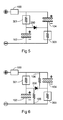
- Fig. 5 is a schematic view showing a circuit of the present invention with an electric load comprised of impedance.
- an electric load comprised of impedance.
- Fig. 5 is comprised of:
- the time of voltage drop at the impedance 301 and 303 in the course of discharging, or the time of extended time when the power is interrupted may have its time constant regulated by having both ends of the first and the second capacitors 102, 104 to respectively connect in parallel with a fist and a second resistances 105, 106.
- circuit of another preferred embodiment yet of the present invention as illustrated in Fig. 6 provided with additional resistance is comprised of:
- the electric load selected in practice for the circuit installation of the present invention allowing full voltage activation, division voltage operation, and delayed breaking may be related to a power driven load providing various of characteristics by voltage, e.g., (1) EM effect applied installation provided with excitement coil including EM breaking installation, relay, EM clutch, EM switch, solenoid, EM iron, EM lock, spiral coil, etc., (2) motor, (3) excitement winding of a power generator, (4) impedance including resistance impedance, coil containing resistance impedance, or power drive installation or device containing resistance impedance; and (5) other power driven installation provided with various features by voltage.
- One or a plurality of same or different power driven installation may be selected from those loads described above to constitute an electric load.
Landscapes
- Engineering & Computer Science (AREA)
- Power Engineering (AREA)
- Business, Economics & Management (AREA)
- Emergency Management (AREA)
- Direct Current Feeding And Distribution (AREA)
- Dc-Dc Converters (AREA)
- Charge And Discharge Circuits For Batteries Or The Like (AREA)
- Relay Circuits (AREA)
Abstract
Description
- The present invention is related to a circuit installation, and more particularly, to one that controls a power load taking advantage of charging, discharging and division voltage features of capacitor to provide activation and operation features different from those provided by a conventional ON-OFF switch.
- The pattern of control and operation of an electric load by conventional power switches usually involves ON or OFF only without the capacity to change the input voltage to the load.
- The primary purpose of the present invention is to provide a circuit installation that is capable of full voltage activation, division voltage operation and delayed breaking. To achieve the purpose, the present invention by taking advantage of the features of a capacitor that integral boosting voltage in charging and differential dropping voltage in discharging connects the capacitor in series with an electric load; two sets of the said capacitor connected in series and the device of electric load are then connected in series in opposite sequence before being connected in parallel; and a diode is connected in series in positive direction at where between two sets of electric loads according to the flowing direction of currents from both sets of electric load. Upon inputting DC power to charge the capacitor through the electric load thus to subject both electric loads respectively connected in series to the capacitor in the series circuits to 100% voltage; and later the charging voltage at the capacitor rises to create balanced division voltage respectively between both electric loads connected in parallel with the capacitor. At such time, both electric loads in the series circuits are in the status of series high resistance and low amperage to achieve the purposes of full voltage activation, division voltage operation, and delayed breaking. The electric load includes EM effect load or resistance load.
-
-
Fig. 1 is a schematic view showing a circuit of the present invention. -
Fig. 2 is a schematic view showing that the circuit of the present invention inFig. 1 is provided with additional resistance. -
Fig. 3 is a schematic view showing a circuit of electric load in the present invention comprised of resistance and EM effect electric load. -
Fig. 4 is a schematic view showing that the circuit of the present invention inFig. 3 is provided with additional resistance. -
Fig. 5 is a schematic view showing a circuit of electric load in the present invention comprised of resistance. -
Fig. 6 is a schematic view showing that the circuit of the present invention inFig. 5 is provided with additional resistance. - Referring to
Fig. 1 , a preferred embodiment of the present invention is comprised of: - --- EM effect
electric loads - --- the first EM effect
electric load 101, provided to constitute a first series circuit by connecting in series with afirst capacitor 102 in the same direction of polarity; - --- a
second capacitor 104, provided to constitute a second series circuit by connecting in series with the second EM effectelectric load 103 in the same direction of polarity; - --- both
capacitors electric loads source switch 100; and - --- a
diode 200, coupled to where between the coupling point of the first EM effectelectric load 101 and thefirst capacitor 102 in the first series circuit and that of the second EM effectelectric load 103 and thesecond capacitor 104 in the second series circuit and indicating series in the same direction of polarity with the first and the second EM effectelectric loads - Wherein, the operation function of the present invention as illustrated in
Fig. 1 involves - (1) With the
source switch 100 is ON, DC power charges thefirst capacitor 102 via the first EM effectelectric load 101 and charges thesecond capacitor 104 via the second EM effectelectric load 103; meanwhile, both of the first and the second EM effectelectric loads electric loads second capacitors - (2) When the voltage of the electric load drops and gets stabilized at the series division voltage values of the first and the second EM effect
electric loads diode 200 in the same direction to be divided by the series resistance value of the first and the second EM effectelectric loads - (3) With the
source switch 100 is OFF or during transient drop of source voltage, thefirst capacitor 102 discharges the second EM effectelectric load 103 and thesecond capacitor 104 discharges the first EM effectelectric load 101 to delay the time for circuit breaking. - In the circuit illustrated in
Fig. 1 , the time of voltage drop at the first and the second EM effectelectric loads second capacitors second resistances -
Fig. 2 shows another preferred embodiment of the present invention with an additional resistance added to the circuit of the preferred embodiment illustrated inFig. 1 . The second preferred embodiment is comprised of: - --- EM effect
electric loads - --- the first EM effect
electric load 101, provided to constitute a first series circuit by connecting in series with afirst capacitor 102 in the same direction of polarity; - --- a
second capacitor 104, provided to constitute a second series circuit by connecting in series with the second EM effectelectric load 103 in the same direction of polarity; - --- both
capacitors electric loads source switch 100; and - --- the
diode 200, coupled to where between the coupling point of the first EM effectelectric load 101 and thefirst capacitor 102 in the first series circuit and that of the second EM effectelectric load 103 and thesecond capacitor 104 in the second series circuit and indicating series in the same direction of polarity with the first and the second EM effectelectric loads - --- the
first resistance 105, comprised of resistance impedance, or any coils containing resistance impedance, or power driven installation or device containing resistance impedance; connected in parallel with both ends of thefirst capacitor 102 to facilitate the discharging rate at thefirst capacitor 102 when the division voltage at the second EM effectelectric load 103 drops or is interrupted; and - --- the
second resistance 106, comprised of resistance impedance, or any coils containing resistance impedance, or power driven installation or device containing resistance impedance; connected in parallel with both ends of thesecond capacitor 104 to facilitate the discharging rate at thesecond capacitor 104 when the division voltage at the first EM effectelectric load 101 drops or is interrupted. - The operational function of the preferred embodiment illustrated in
Fig. 2 involves: - (1) With the
source switch 100 is ON, DC power charges thefirst capacitor 102 via the first EM effectelectric load 101 and charges thesecond capacitor 104 via the second EM effectelectric load 103; meanwhile, both of the first and the second EM effectelectric loads electric loads second capacitors first resistance 105 connected in parallel with thefirst capacitor 102 and thesecond resistance 106 connected in parallel with thesecond capacitor 104 extend the time of voltage drop respectively at the first and the second EM effectelectric loads - (2) When the voltage of the electric load drops and gets stabilized at the series division voltage values of the first and the second EM effect
electric loads diode 200 in the same direction to be divided by the series resistance value of the first and the second EM effectelectric loads - (3) With the
source switch 100 is OFF or during transient drop of source voltage, thefirst capacitor 102 discharges thefirst resistance 105 and the second EM effectelectric load 103; and thesecond capacitor 104 discharges thesecond resistance 106 and the first EM effectelectric load 101 to delay the time for circuit breaking. - The circuit installation allowing full voltage activation, division voltage operation and delayed breaking while having both EM effect electric loads to serve as electric loads may also have an
impedance 301 serving as a resistance electric load for voltage drop thus to drive the single EM effectelectric load 103. -
Fig. 3 shows that a circuit of electric load in another preferred embodiment yet of the present invention is comprised of an impedance and EM effect electric load. The third preferred embodiment is comprised of: - --- the EM effect
electric load 103, related to an electric drive installation giving various features depending on the voltage, e.g., an EM effect installation or an installation converting EM force into mechanical energy; - --- the
impedance 301, comprised of resistance impedance, or any coils containing resistance impedance, or power driven installation or device containing resistance impedance; - --- the
impedance 301, provided for connecting thefirst capacitor 102 in series indicating the same direction of polarity to constitute a first series circuit; - --- a
second capacitor 104, provided to constitute a second series circuit by connecting in series with the EM effectelectric load 103 in the same direction of polarity; - --- both of the first and the second series circuits are connected to each other in parallel indicating the same polarity to be subject to control by a
source switch 100; and - --- the
diode 200, coupled to where between the coupling point of theimpedance 301 and thefirst capacitor 102 in the first series circuit and that of the EM effectelectric load 103 and thesecond capacitor 104 in the second series circuit and indicating series in the same direction of polarity with theimpedance 301 and the EM effectelectric loads 103 to permit flow of DC power. - The operational function of the preferred embodiment illustrated in
Fig. 3 involves: - (1) With the
source switch 100 is ON, DC power charges thefirst capacitor 102 via theimpedance 301 and charges thesecond capacitor 104 via the EM effectelectric load 103; meanwhile, both of theimpedance 301 and the EM effectelectric load 103 are subject to 100% voltage and the voltage gradually drops at theimpedance 301 and the EM effectelectric load 103 due to that the charging voltage respectively at the first and thesecond capacitors - (2) When the voltage of the electric load drops and gets stabilized at the series division voltage values of the
impedance 301 and the EM effectelectric load 103, the amperage drops to where equal to the difference of DC source voltage less the voltage VF of thediode 200 in the same direction to be divided by the series resistance value of theimpedance 301 and the EM effectelectric load 103. - (3) With the
source switch 100 is OFF or during transient drop of source voltage, thefirst capacitor 102 discharges the EM effectelectric load 103; and thesecond capacitor 104 discharges theimpedance 301 to delay the time for circuit breaking. - In the circuit illustrated in
Fig. 3 , the time of voltage drop at the EM effectelectric load 103 and theimpedance 301 in the course of discharging, or the time of extended time when the power is interrupted may have its time constant regulated by having both ends of the first and thesecond capacitors second resistances -
Fig. 4 shows another preferred embodiment yet of the present invention with an additional resistance added to the circuit of the preferred embodiment illustrated inFig. 3 . The preferred embodiment illustrated inFig. 4 is comprised of: - --- the EM effect
electric load 103, related to an electric drive installation giving various features depending on the voltage, e.g., an EM effect installation or an installation converting EM force into mechanical energy; - --- the
impedance 301, comprised of resistance impedance, or any coils containing resistance impedance, or power driven installation or device containing resistance impedance; - --- the
impedance 301, provided for connecting thefirst capacitor 102 in series indicating the same direction of polarity to constitute a first series circuit; - --- a
second capacitor 104, provided to constitute a second series circuit by connecting in series with the EM effectelectric load 103 in the same direction of polarity; - --- both of the first and the second series circuits are connected in parallel of the same polarity to be subject to control by a
source switch 100; and - --- the
diode 200, coupled to where between the coupling point of theimpedance 301 and the first EM effectelectric load 101 in the first series circuit and that of the EM effectelectric load 103 and thesecond capacitor 104 in the second series circuit and indicating series in the same direction of polarity with theimpedance 301 and the EM effectelectric load 103 to permit flow of DC power; - --- the
first resistance 105, comprised of resistance impedance, or any coils containing resistance impedance, or power driven installation or device containing resistance impedance; connected in parallel with both ends of thefirst capacitor 102 to facilitate the discharging rate at thefirst capacitor 102 when the division voltage at the second EM effectelectric load 103 drops or is interrupted; and - --- the
second resistance 106, comprised of resistance impedance, or any coils containing resistance impedance, or power driven installation or device containing resistance impedance; connected in parallel with both ends of thesecond capacitor 104 to facilitate the discharging rate at thesecond capacitor 104 when the division voltage atimpedance 301 drops or is interrupted; thesecond resistance 106 may or may not be provided depending on the characteristics of theresistance 301 connected in parallel. - The operational function of the preferred embodiment illustrated in
Fig. 4 involves: - (1) With the
source switch 100 is ON, DC power charges thefirst capacitor 102 via theimpedance 301 and charges thesecond capacitor 104 via the EM effectelectric load 103; meanwhile, both of theimpedance 301 and the EM effectelectric load 103 are subject to 100% voltage and the voltage gradually drops at theimpedance 301 and the EM effectelectric load 103 due to that the charging voltage respectively at the first and thesecond capacitors first resistance 105 connected in parallel with thefirst capacitor 102 and thesecond resistance 106 connected in parallel with thesecond capacitor 104 extend the time of voltage drop respectively at theimpedance 301 and the EM effectelectric load 103. - (2) When the voltage of the electric load drops and gets stabilized at the series division voltage values of the
impedance 301 and the EM effectelectric load 103, the amperage drops to where equal to the difference of DC source voltage less the voltage VF of thediode 200 in the same direction to be divided by the series resistance value of theimpedance 301 and the EM effectelectric load 103. - (3) With the
source switch 100 is OFF or during transient drop of source voltage, thefirst capacitor 102 discharges thefirst resistance 105 and the EM effectelectric load 103; and thesecond capacitor 104 discharges thesecond resistance 106 and theimpedance 301 to delay the time for circuit breaking. - The circuit installation allowing full voltage activation, division voltage operation and delayed breaking may have the electric load comprised of the
impedance 301 and anotherimpedance 303. -
Fig. 5 is a schematic view showing a circuit of the present invention with an electric load comprised of impedance. In the preferred embodiment illustrated inFig. 5 is comprised of: - --- the
impedance - --- the
impedance 301, provided for connecting thefirst capacitor 102 in series indicating the same direction of polarity to constitute a first series circuit; - --- the
second capacitor 104, provided for connecting theimpedance 303 in series indicating the same direction of polarity to constitute a second series circuit; - --- both of the first and the second series circuits are connected in parallel of the same polarity to be subject to control by a
source switch 100; and - --- the
diode 200, coupled to where between the coupling point of theimpedance 301 and thefirst capacitor 102 in the first series circuit and that of theimpedance 303 and thesecond capacitor 104 in the second series circuit and indicating series in the same direction of polarity with theimpedance 301 and anotherimpedance 303 to permit flow of DC power. - The preferred embodiment illustrated in
Fig. 5 operates as follows: - (1) With the
source switch 100 is ON, DC power charges thefirst capacitor 102 via theimpedance 301 and charges thesecond capacitor 104 via thesecond impedance 303; meanwhile, both of theimpedance 301 and thesecond impedance 303 are subject to 100% voltage and the voltage gradually drops at theimpedance 301 and thesecond impedance 303 due to that the charging voltage respectively at the first and thesecond impedances - (2) When the voltage of the electric load drops and gets stabilized at the series division voltage values of the
impedance 301 and thesecond impedance 303, the amperage drops to where equal to the difference of DC source voltage less the voltage VF of thediode 200 in the same direction to be divided by the series resistance value of theimpedance 301 and thesecond impedance 303. - (3) With the
source switch 100 is OFF or during transient drop of source voltage, thefirst capacitor 102 discharges thefirst impedance 301; and thesecond capacitor 104 discharges thesecond impedance 303 to delay the time for circuit breaking. - In the circuit illustrated in
Fig. 5 , the time of voltage drop at theimpedance second capacitors second resistances - The circuit of another preferred embodiment yet of the present invention as illustrated in
Fig. 6 provided with additional resistance is comprised of: - --- the
impedance - --- the
impedance 301, provided for connecting thefirst capacitor 102 in series indicating the same direction of polarity to constitute a first series circuit; - --- the
second capacitor 104, provided for connecting theimpedance 303 in series indicating the same direction of polarity to constitute a second series circuit; - --- both of the first and the second series circuits are connected in parallel of the same polarity to be subject to control by a
source switch 100; - --- the
diode 200, coupled to where between the coupling point of theimpedance 301 and thefirst capacitor 102 in the first series circuit and that of theimpedance 303 and thesecond capacitor 104 in the second series circuit and indicating series in the same direction of polarity with theimpedance 301 and anotherimpedance 303 to permit flow of DC power; - --- the
first resistance 105, comprised of resistance impedance, or any coils containing resistance impedance, or power driven installation or device containing resistance impedance; connected in parallel with both ends of thefirst capacitor 102 to facilitate the discharging rate at thefirst capacitor 102 when the division voltage at theimpedance 303 drops or is interrupted; and thefirst resistance 105 may or may not be provided depending on the characteristics of theresistance 303 connected in parallel; - --- the
second resistance 106, comprised of resistance impedance, or any coils containing resistance impedance, or power driven installation or device containing resistance impedance; connected in parallel with both ends of thesecond capacitor 104 to facilitate the discharging rate at thesecond capacitor 104 when the division voltage atimpedance 301 drops or is interrupted; and thesecond resistance 106 may or may not be provided depending on the characteristics of theresistance 301 connected in parallel. - The preferred embodiment of the present invention operates as follows:
- (1) With the
source switch 100 is ON, DC power charges thefirst capacitor 102 via theimpedance 301 and charges thesecond capacitor 104 via thesecond impedance 303; meanwhile, both of theimpedance 301 and thesecond impedance 303 are subject to 100% voltage and the voltage gradually drops at theimpedance 301 and thesecond impedance 303 due to that the charging voltage respectively at the first and thesecond impedances first resistance 105 connected in parallel with thefirst capacitor 102 as well as thesecond resistance 106 connected in parallel with thesecond capacitor 106 are capable of extending the voltage drop time respectively for theimpedance 301 and the second EM effectelectric load 103. - (2) When the voltage of the electric load drops and gets stabilized at the series division voltage values of the
impedance 301 and thesecond impedance 303, the amperage drops to where equal to the difference of DC source voltage less the voltage VF of thediode 200 in the same direction to be divided by the series resistance value of theimpedance 301 and thesecond impedance 303. - (3) With the
source switch 100 is OFF or during transient drop of source voltage, thefirst capacitor 102 discharges thefirst impedance 301; and thesecond capacitor 104 discharges thesecond impedance 303 to delay the time for circuit breaking - The electric load selected in practice for the circuit installation of the present invention allowing full voltage activation, division voltage operation, and delayed breaking may be related to a power driven load providing various of characteristics by voltage, e.g., (1) EM effect applied installation provided with excitement coil including EM breaking installation, relay, EM clutch, EM switch, solenoid, EM iron, EM lock, spiral coil, etc., (2) motor, (3) excitement winding of a power generator, (4) impedance including resistance impedance, coil containing resistance impedance, or power drive installation or device containing resistance impedance; and (5) other power driven installation provided with various features by voltage. One or a plurality of same or different power driven installation may be selected from those loads described above to constitute an electric load.
- In summary, the circuit configuration disclosed in the present invention for allowing full voltage activation, division voltage operation, and delayed breaking gives precise function and innovative creativity; therefore, this application for patent is duly filed accordingly.
Claims (15)
- A circuit installation capable of full voltage activation, division voltage operation and delayed breaking by taking advantage of the features of a capacitor that integral boosting voltage in charging and differential dropping voltage in discharging connects the capacitor in series with an electric load; two sets of the said capacitor connected in series and the device of electric load are then connected in series in opposite sequence before being connected in parallel; and a diode being connected in series in positive direction at where between two sets of electric loads according to the flowing direction of currents from both sets of electric load; upon inputting DC power to charge the capacitor through the electric load to subject both electric loads respectively connected in series to the capacitor in the series circuits to 100% voltage; and later the charging voltage at the capacitor rises to create balanced division voltage respectively between both electric loads connected in parallel with the capacitor; both electric loads in the series circuits being in the status of series high resistance and low amperage to achieve the purposes of full voltage activation, division voltage operation, and delayed breaking; and the electric load includes EM effect load or resistance load.
- The circuit installation capable of full voltage activation, division voltage operation and delayed breaking as claimed in Claim 1 is comprised of:--- EM effect electric loads (101, 103), each related to an electric drive installation giving various features depending on the voltage, e.g., an EM effect installation or an installation converting EM force into mechanical energy;--- the first EM effect electric load (101), provided to constitute a first series circuit by connecting in series with a first capacitor (102) in the same direction of polarity;--- a second capacitor (104), provided to constitute a second series circuit by connecting in series with the second EM effect electric load (103) in the same direction of polarity;--- both capacitors (102, 104) and devices of both EM effect electric loads (101, 103) in the first and the second series circuits are connected in series in opposite sequence before being connected in parallel indicating the same polarity to be subject to control by a source switch (100); and--- a diode (200), coupled to where between the coupling point of the first EM effect electric load (101) and the first capacitor (102) in the first series circuit and that of the second EM effect electric load (103) and the second capacitor (104) in the second series circuit and indicating series in the same direction of polarity with the first and the second EM effect electric loads (101, 103) to permit flow of DC power.
- The circuit installation capable of full voltage activation, division voltage operation and delayed breaking as claimed in Claim 2, wherein the circuit operates as follows:(1) With the source switch (100) is ON, DC power charges the first capacitor (102) via the first EM effect electric load (101) and charges the second capacitor (104) via the second EM effect electric load (103); meanwhile, both of the first and the second EM effect electric loads (101, 103) are subject to 100% voltage and the voltage gradually drops at each of the first and the second EM effect electric loads (101, 103) due to that the charging voltage respectively at the first and the second capacitors (102, 104) indicates integral curve rising status;(2) When the voltage of the electric load drops and gets stabilized at the series division voltage values of the first and the second EM effect electric loads (101, 103), the amperage drops to where equal to the difference of DC source voltage less the voltage VF of the diode 200 in the same direction to be divided by the series resistance value of the first and the second EM effect electric loads (101, 103);(3) With the source switch (100) is OFF or during transient drop of source voltage, the first capacitor (102) discharges the second EM effect electric load (103) and the second capacitor (104) discharges the first EM effect electric load (101) to delay the time for circuit breaking.
- The circuit installation capable of full voltage activation, division voltage operation and delayed breaking as claimed in Claim 2, wherein the time of voltage drop at the first and the second EM effect electric loads (101, 103) in the course of feeding the power, or the time of extended circuit breaking may have its time constant regulated by having both ends of the first and the second capacitors (102, 104) to respectively connect in parallel with a fist and a second resistances (105, 106) is comprised of:--- EM effect electric loads (101, 103), each related to an electric drive installation giving various features depending on the voltage, e.g., an EM effect installation or an installation converting EM force into mechanical energy;--- the first EM effect electric load (101), provided to constitute a first series circuit by connecting in series with a first capacitor (102) in the same direction of polarity;--- a second capacitor (104), provided to constitute a second series circuit by connecting in series with the second EM effect electric load (103) in the same direction of polarity;--- both capacitors (102, 104) and devices of both EM effect electric loads (101, 103) in the first and the second series circuits are connected in series in opposite sequence before being connected in parallel indicating the same polarity to be subject to control by a source switch (100); and--- the diode (200), coupled to where between the coupling point of the first EM effect electric load (101) and the first capacitor (102) in the first series circuit and that of the second EM effect electric load (103) and the second capacitor (104) in the second series circuit and indicating series in the same direction of polarity with the first and the second EM effect electric loads (101, 103) to permit flow of DC power;--- the first resistance (105), comprised of resistance impedance, or any coils containing resistance impedance, or power driven installation or device containing resistance impedance; connected in parallel with both ends of the first capacitor (102) to facilitate the discharging rate at the first capacitor (102) when the division voltage at the second EM effect electric load (103) drops or is interrupted; and--- the second resistance (106), comprised of resistance impedance, or any coils containing resistance impedance, or power driven installation or device containing resistance impedance; connected in parallel with both ends of the second capacitor (104) to facilitate the discharging rate at the second capacitor (104) when the division voltage at the first EM effect electric load (101) drops or is interrupted.
- The circuit installation capable of full voltage activation, division voltage operation and delayed breaking as claimed in Claim 4, wherein, the circuit operates as follows:(1) With the source switch (100) is ON, DC power charges the first capacitor (102) via the first EM effect electric load (101) and charges the second capacitor (104) via the second EM effect electric load (103); meanwhile, both of the first and the second EM effect electric loads (101, 103) are subject to 100% voltage and the voltage gradually drops at each of the first and the second EM effect electric loads (101, 103) due to that the charging voltage respectively at the first and the second capacitors (102, 104) indicates integral curve rising status; the first resistance (105) connected in parallel with the first capacitor (102) and the second resistance (106) connected in parallel with the second capacitor (104) extend the time of voltage drop respectively at the first and the second EM effect electric loads (101, 103);(2) When the voltage of the electric load drops and gets stabilized at the series division voltage values of the first and the second EM effect electric loads (101, 103), the amperage drops to where equal to the difference of DC source voltage less the voltage of the diode 200 VF in the same direction to be divided by the series resistance value of the first and the second EM effect electric loads (101, 103);(3) With the source switch (100) is OFF or during transient drop of source voltage, the first capacitor (102) discharges the first resistance (105) and the second EM effect electric load (103); and the second capacitor (104) discharges the second resistance (106) and the first EM effect electric load (101) to delay the time for circuit breaking.
- The circuit installation capable of full voltage activation, division voltage operation and delayed breaking as claimed in Claim 1, wherein an impedance (301) being provided as a resistance electric load provided with voltage drop function to drive a single EM effect electric load (103) is comprised of:--- the EM effect electric load (103), related to an electric drive installation giving various features depending on the voltage, e.g., an EM effect installation or an installation converting EM force into mechanical energy;--- the impedance (301), comprised of resistance impedance, or any coils containing resistance impedance, or power driven installation or device containing resistance impedance;--- the impedance (301), provided for connecting the first capacitor (102) in series indicating the same direction of polarity to constitute a first series circuit;--- a second capacitor (104), provided to constitute a second series circuit by connecting in series with the EM effect electric load (103) in the same direction of polarity;--- both of the first and the second series circuits are connected to each other in parallel indicating the same polarity to be subject to control by a source switch (100); and--- the diode (200), coupled to where between the coupling point of the impedance (301) and the first capacitor (102) in the first series circuit and that of the EM effect electric load (103) and the second capacitor (104) in the second series circuit and indicating series in the same direction of polarity with the impedance (301) and the EM effect electric load (103) to permit flow of DC power.
- The circuit installation capable of full voltage activation, division voltage operation and delayed breaking as claimed in Claim 6, wherein the circuit operates as follows:(1) With the source switch (100) is ON, DC power charges the first capacitor (102) via the impedance (301) and charges the second capacitor (104) via the EM effect electric load (103); meanwhile, both of the impedance (301) and the EM effect electric load (103) are subject to 100% voltage and the voltage gradually drops at the impedance (301) and the EM effect electric load (103) due to that the charging voltage respectively at the first and the second capacitors (102, 104) indicates integral curve rising status;(2) When the voltage of the electric load drops and gets stabilized at the series division voltage values of the impedance (301) and the EM effect electric load (103), the amperage drops to where equal to the difference of DC source voltage less the voltage VF of the diode 200 in the same direction to be divided by the series resistance value of the impedance (301) and the EM effect electric load (103);(3) With the source switch (100) is OFF or during transient drop of source voltage, the first capacitor (102) discharges the EM effect electric load (103); and the second capacitor (104) discharges the impedance (301) to delay the time for circuit breaking.
- The circuit installation capable of full voltage activation, division voltage operation and delayed breaking as claimed in Claim 6, wherein the time of voltage drop at the EM effect electric load (103) and the impedance (301) in the course of feeding the power, or the time of extended circuit breaking may have its time constant regulated by having both ends of the first and the second capacitors (102, 104) to respectively connect in parallel with a fist and a second resistances (105, 106) is comprised of:--- the EM effect electric load (103), related to an electric drive installation giving various features depending on the voltage, e.g., an EM effect installation or an installation converting EM force into mechanical energy;--- the impedance (301), comprised of resistance impedance, or any coils containing resistance impedance, or power driven installation or device containing resistance impedance;--- the impedance (301), provided for connecting the first capacitor (102) in series indicating the same direction of polarity to constitute a first series circuit;--- a second capacitor (104), provided to constitute a second series circuit by connecting in series with the EM effect electric load (103) in the same direction of polarity;--- both of the first and the second series circuits are connected in parallel of the same polarity to be subject to control by a source switch (100); and--- the diode (200), coupled to where between the coupling point of the impedance (301) and the first EM effect electric load (101) in the first series circuit and that of the EM effect electric load (103) and the second capacitor (104) in the second series circuit and indicating series in the same direction of polarity with the impedance (301) and the EM effect electric load (103) to permit flow of DC power;--- the first resistance (105), comprised of resistance impedance, or any coils containing resistance impedance, or power driven installation or device containing resistance impedance; connected in parallel with both ends of the first capacitor (102) to facilitate the discharging rate at the first capacitor (102) when the division voltage at the second EM effect electric load (103) drops or is interrupted; and--- the second resistance (106), comprised of resistance impedance, or any coils containing resistance impedance, or power driven installation or device containing resistance impedance; connected in parallel with both ends of the second capacitor (104) to facilitate the discharging rate at the second capacitor (104) when the division voltage at impedance (301) drops or is interrupted; the second resistance (106) may or may not be provided depending on the characteristics of the resistance (301) connected in parallel.
- The circuit installation capable of full voltage activation, division voltage operation and delayed breaking as claimed in Claim 8, wherein the circuit operates as follows:(1) With the source switch (100) is ON, DC power charges the first capacitor (102) via the impedance (301) and charges the second capacitor (104) via the EM effect electric load (103); meanwhile, both of the impedance (301) and the EM effect electric load (103) are subject to 100% voltage and the voltage gradually drops at the impedance (301) and the EM effect electric load (103) due to that the charging voltage respectively at the first and the second capacitors (102, 104) indicates integral curve rising status; the first resistance (105) connected in parallel with the first capacitor (102) and the second resistance (106) connected in parallel with the second capacitor (104) extend the time of voltage drop respectively at the impedance (301) and the EM effect electric load (103);(2) When the voltage of the electric load drops and gets stabilized at the series division voltage values of the impedance (301) and the EM effect electric load (103), the amperage drops to where equal to the difference of DC source voltage less the voltage VF of the diode 200 in the same direction to be divided by the series resistance value of the impedance (301) and the EM effect electric load (103);(3) With the source switch (100) is OFF or during transient drop of source voltage, the first capacitor (102) discharges the first resistance (105) and the EM effect electric load (103); and the second capacitor (104) discharges the second resistance (106) and the impedance (301) to delay the time for circuit breaking.
- The circuit installation capable of full voltage activation, division voltage operation and delayed breaking as claimed in Claim 1, wherein the circuit further includes an electric load comprised of an impedance (301) and (303) is comprised of:--- the impedance (301) and (303), each comprised of resistance impedance, or any coils containing resistance impedance, or power driven installation or device containing resistance impedance; both may be comprised of the same or different types with their resistance values may be of the same or not;--- the impedance (301), provided for connecting the first capacitor (102) in series indicating the same direction of polarity to constitute a first series circuit;--- the second capacitor (104), provided for connecting the impedance (303) in series indicating the same direction of polarity to constitute a second series circuit;--- both of the first and the second series circuits are connected in parallel of the same polarity to be subject to control by a source switch (100); and--- the diode (200), coupled to where between the coupling point of the impedance (301) and the first capacitor (102) in the first series circuit and that of the impedance (303) and the second capacitor (104) in the second series circuit and indicating series in the same direction of polarity with the impedance (301) and another impedance (303) to permit flow of DC power.
- The circuit installation capable of full voltage activation, division voltage operation and delayed breaking as claimed in Claim 10, wherein the circuit operates as follows:(1) With the source switch (100) is ON, DC power charges the first capacitor (102) via the impedance (301) and charges the second capacitor (104) via the second impedance (303); meanwhile, both of the impedance (301) and the second impedance (303) are subject to 100% voltage and the voltage gradually drops at the impedance (301) and the second impedance (303) due to that the charging voltage respectively at the first and the second impedances (301, 303) indicates integral curve rising status;(2) When the voltage of the electric load drops and gets stabilized at the series division voltage values of the impedance (301) and the second impedance (303), he amperage drops to where equal to the difference of DC source voltage less the voltage VF of the diode 200 in the same direction to be divided by the series resistance value of the impedance (301) and the second impedance (303);(3) With the source switch (100) is OFF or during transient drop of source voltage, the first capacitor (102) discharges the first impedance (301); and the second capacitor (104) discharges the second impedance (303) to delay the time for circuit breaking.
- The circuit installation capable of full voltage activation, division voltage operation and delayed breaking as claimed in Claim 10, wherein the time of voltage drop at the impedance (301) and (303) in the course of feeding the power, or the time of extended circuit breaking may have its time constant regulated by having both ends of the first and the second capacitors (102, 104) to respectively connect in parallel with a fist and a second resistances (105, 106) is comprised of:--- the impedance (301) and (303), each comprised of resistance impedance, or any coils containing resistance impedance, or power driven installation or device containing resistance impedance; both may be comprised of the same or different types with their resistance values may be of the same or not;--- the impedance (301), provided for connecting the first capacitor (102) in series indicating the same direction of polarity to constitute a first series circuit;--- the second capacitor (104), provided for connecting the impedance (303) in series indicating the same direction of polarity to constitute a second series circuit;--- both of the first and the second series circuits are connected in parallel of the same polarity to be subject to control by a source switch (100);--- the diode (200), coupled to where between the coupling point of the impedance (301) and the first capacitor (102) in the first series circuit and that of the impedance (303) and the second capacitor (104) in the second series circuit and indicating series in the same direction of polarity with the impedance (301) and another impedance (303) to permit flow of DC power;--- the first resistance (105), comprised of resistance impedance, or any coils containing resistance impedance, or power driven installation or device containing resistance impedance; connected in parallel with both ends of the first capacitor (102) to facilitate the discharging rate at the first capacitor (102) when the division voltage at the impedance (303) drops or is interrupted; and the first resistance (105) may or may not be provided depending on the characteristics of the resistance (303) connected in parallel;--- the second resistance (106), comprised of resistance impedance, or any coils containing resistance impedance, or power driven installation or device containing resistance impedance; connected in parallel with both ends of the second capacitor (104) to facilitate the discharging rate at the second capacitor (104) when the division voltage at impedance (301) drops or is interrupted; and the second resistance (106) may or may not be provided depending on the characteristics of the resistance (301) connected in parallel.
- The circuit installation capable of full voltage activation, division voltage operation and delayed breaking as claimed in Claim 12, wherein the circuit operates as follows:(1) With the source switch (100) is ON, DC power charges the first capacitor (102) via the impedance (301) and charges the second capacitor (104) via the second impedance (303); meanwhile, both of the impedance (301) and the second impedance (303) are subject to 100% voltage and the voltage gradually drops at the impedance (301) and the second impedance (303) due to that the charging voltage respectively at the first and the second impedances (301, 303) indicates integral curve rising status; and the first resistance (105) connected in parallel with the first capacitor (102) as well as the second resistance (106) connected in parallel with the second capacitor (104) are capable of extending the voltage drop time respectively for the impedance (301) and the second EM effect electric load (103);(2) When the voltage of the electric load drops and gets stabilized at the series division voltage values of the impedance (301) and the second impedance (303), the amperage drops to where equal to the difference of DC source voltage less the voltage VF of the diode 200 in the same direction to be divided by the series resistance value of the impedance (301) and the second impedance (303);(3) With the source switch (100) is OFF or during transient drop of source voltage, the first capacitor (102) discharges the first impedance (301); and the second capacitor (104) discharges the second impedance (303) to delay the time for circuit breaking.
- The circuit installation capable of full voltage activation, division voltage operation and delayed breaking as claimed in Claim 1, wherein the electric load selected may be related to a power driven load providing various of characteristics by voltage, e.g., (1) EM effect applied installation provided with excitement coil including EM breaking installation, relay, EM clutch, EM switch, solenoid, EM iron, EM lock, spiral coil, etc., (2) motor, (3) excitement winding of a power generator, (4) impedance including resistance impedance, coil containing resistance impedance, or power drive installation or device containing resistance impedance; and (5) other power driven installation provided with various features by voltage; and one or a plurality of same or different power driven installation may be selected from those loads described above to constitute an electric load.
- A circuit installation for executing full voltage activation, division voltage operation, and delayed breaking of an electric load by providing capacitance means for increasing the power to the load to promote its activation performance, or for reducing operational power in the course of operation by the load to save power or limit operation performance of the load.
Priority Applications (11)
| Application Number | Priority Date | Filing Date | Title |
|---|---|---|---|
| US11/526,585 US7839105B2 (en) | 2006-09-26 | 2006-09-26 | Circuit installation capable of full voltage activation, division voltage operation and delayed breaking |
| TW96137754A TWI470397B (en) | 2007-10-08 | 2007-10-08 | Full-voltage start-up partial pressure operation and delayed power-off circuit device |
| EP07254872A EP2071425B1 (en) | 2006-09-26 | 2007-12-14 | Circuit installation capable of full voltage activation, division voltage operation and delayed breaking |
| AT07254872T ATE508404T1 (en) | 2006-09-26 | 2007-12-14 | CIRCUIT DEVICE WITH FULL VOLTAGE ACTIVATION, VOLTAGE DIVIDER OPERATION AND DELAYED SWITCHING CAPABILITY |
| DE602007014388T DE602007014388D1 (en) | 2006-09-26 | 2007-12-14 | Circuit device capable of full voltage activation, voltage divider operation and delayed switching |
| CN2008100858360A CN101540550B (en) | 2007-10-08 | 2008-03-21 | Full-voltage starting voltage division work and delay power-off circuit device |
| KR1020080027290A KR101565160B1 (en) | 2007-10-08 | 2008-03-25 | Voltage Starter Operation and Circuit Break Delay |
| JP2008078317A JP5302557B2 (en) | 2007-10-08 | 2008-03-25 | Full pressure starting partial pressure operation and circuit interruption delay device |
| CA2626949A CA2626949C (en) | 2006-09-26 | 2008-03-25 | Circuit installation capable of full voltage activation, division voltage operation and delayed braking |
| AU2008201386A AU2008201386B2 (en) | 2006-09-26 | 2008-03-26 | Circuit installation capable of full voltage activation, division voltage operation and delayed breaking |
| US12/907,194 US7911164B2 (en) | 2006-09-26 | 2010-10-19 | Circuit installation capable of full voltage activation, division voltage operation and delayed breaking |
Applications Claiming Priority (8)
| Application Number | Priority Date | Filing Date | Title |
|---|---|---|---|
| US11/526,585 US7839105B2 (en) | 2006-09-26 | 2006-09-26 | Circuit installation capable of full voltage activation, division voltage operation and delayed breaking |
| TW96137754A TWI470397B (en) | 2007-10-08 | 2007-10-08 | Full-voltage start-up partial pressure operation and delayed power-off circuit device |
| EP07254872A EP2071425B1 (en) | 2006-09-26 | 2007-12-14 | Circuit installation capable of full voltage activation, division voltage operation and delayed breaking |
| CN2008100858360A CN101540550B (en) | 2007-10-08 | 2008-03-21 | Full-voltage starting voltage division work and delay power-off circuit device |
| KR1020080027290A KR101565160B1 (en) | 2007-10-08 | 2008-03-25 | Voltage Starter Operation and Circuit Break Delay |
| JP2008078317A JP5302557B2 (en) | 2007-10-08 | 2008-03-25 | Full pressure starting partial pressure operation and circuit interruption delay device |
| CA2626949A CA2626949C (en) | 2006-09-26 | 2008-03-25 | Circuit installation capable of full voltage activation, division voltage operation and delayed braking |
| AU2008201386A AU2008201386B2 (en) | 2006-09-26 | 2008-03-26 | Circuit installation capable of full voltage activation, division voltage operation and delayed breaking |
Publications (2)
| Publication Number | Publication Date |
|---|---|
| EP2071425A1 true EP2071425A1 (en) | 2009-06-17 |
| EP2071425B1 EP2071425B1 (en) | 2011-05-04 |
Family
ID=50486679
Family Applications (1)
| Application Number | Title | Priority Date | Filing Date |
|---|---|---|---|
| EP07254872A Active EP2071425B1 (en) | 2006-09-26 | 2007-12-14 | Circuit installation capable of full voltage activation, division voltage operation and delayed breaking |
Country Status (7)
| Country | Link |
|---|---|
| US (2) | US7839105B2 (en) |
| EP (1) | EP2071425B1 (en) |
| JP (1) | JP5302557B2 (en) |
| KR (1) | KR101565160B1 (en) |
| CN (1) | CN101540550B (en) |
| DE (1) | DE602007014388D1 (en) |
| TW (1) | TWI470397B (en) |
Cited By (2)
| Publication number | Priority date | Publication date | Assignee | Title |
|---|---|---|---|---|
| DE102018122265B3 (en) * | 2018-09-12 | 2020-02-13 | Phoenix Contact Gmbh & Co. Kg | relay |
| DE102018122269A1 (en) * | 2018-09-12 | 2020-03-12 | Phoenix Contact Gmbh & Co. Kg | Relay module |
Families Citing this family (10)
| Publication number | Priority date | Publication date | Assignee | Title |
|---|---|---|---|---|
| EP2254224A1 (en) * | 2009-05-18 | 2010-11-24 | SMA Solar Technology AG | Method for discharging a filter capacitor at the output of an inverter device and inverter device |
| TWI403181B (en) | 2009-06-23 | 2013-07-21 | Richtek Technology Corp | Power off delay circuit and method, and audio system with power off delay |
| US8476863B2 (en) * | 2010-05-17 | 2013-07-02 | Mitchell Andrew Paasch | Energy storage and charging system for a vehicle |
| TWI488207B (en) * | 2012-08-17 | 2015-06-11 | Lite On Electronics Guangzhou | Relay driving device and driving method thereof |
| US9099926B2 (en) * | 2012-10-11 | 2015-08-04 | Hamilton Sundstrand Corporation | System and method for connecting the midpoint of a dual-DC bus to ground |
| US11482878B2 (en) * | 2016-04-15 | 2022-10-25 | Ucap Power, Inc. | Parallel string voltage support |
| CN107561848B (en) * | 2017-08-08 | 2020-11-27 | 嘉兴尚坤科技有限公司 | Automatic positioning circuit for amusement slide projector |
| BE1026605B1 (en) * | 2018-09-12 | 2020-04-09 | Phoenix Contact Gmbh & Co | Relay module |
| CN110828176B (en) * | 2019-11-27 | 2022-01-07 | 东佳电子(郴州)有限公司 | Pulse capacitor for fast discharge unit |
| CN120301227B (en) * | 2025-05-12 | 2025-10-17 | 惠州市乐亿通科技股份有限公司 | Neutral point voltage self-balancing three-level inverter and modulation method |
Citations (4)
| Publication number | Priority date | Publication date | Assignee | Title |
|---|---|---|---|---|
| GB669607A (en) * | 1950-01-10 | 1952-04-02 | Wilfrid Brooke | Improvements in the remote control and protection of electric motors |
| JPH0919145A (en) * | 1995-06-28 | 1997-01-17 | Nec Home Electron Ltd | Switching power supply |
| US6023419A (en) * | 1997-12-08 | 2000-02-08 | Yang; Tai-Her | Capacitor regulated controllable voltage and current power supply |
| EP1119096A2 (en) * | 2000-01-18 | 2001-07-25 | Diehl AKO Stiftung & Co. KG | Voltage stabilising circuit at an ac powered load |
Family Cites Families (16)
| Publication number | Priority date | Publication date | Assignee | Title |
|---|---|---|---|---|
| JPS57127224U (en) * | 1981-01-30 | 1982-08-07 | ||
| JPS6176069A (en) * | 1984-09-20 | 1986-04-18 | Mitsubishi Electric Corp | Converter device |
| JPH02276484A (en) * | 1989-04-18 | 1990-11-13 | Matsushita Electric Ind Co Ltd | Drive circuit for motor |
| US5345161A (en) * | 1992-04-10 | 1994-09-06 | Electroimpact, Inc. | Power supply system for an electromagnetic riveting apparatus |
| JPH07135771A (en) * | 1993-11-09 | 1995-05-23 | Hitachi Ltd | 2-output DC-DC converter |
| IT1271237B (en) * | 1994-09-30 | 1997-05-27 | Whirlpool Italia | DEVICE TO CONTROL THE POWER OF HEATING ELEMENTS |
| KR0139662B1 (en) * | 1995-04-27 | 1998-08-17 | 김광호 | Power balance circuit |
| JPH1070837A (en) * | 1996-08-28 | 1998-03-10 | Nec Corp | Charging and discharge circuit for capacitor for power-supply backup |
| TW359887B (en) * | 1997-11-28 | 1999-06-01 | Winbond Electronics Corp | IC interline protective circuit |
| JPH11341848A (en) * | 1998-05-28 | 1999-12-10 | Nec Shizuoka Ltd | Power supply feeding circuit |
| US6291951B1 (en) * | 2000-03-21 | 2001-09-18 | Valiant Machine & Tool Inc. | Holding brake control circuit for servo-motor |
| AT411412B (en) * | 2000-05-31 | 2003-12-29 | Siemens Ag Oesterreich | BUFFER CIRCUIT |
| US20040130299A1 (en) * | 2001-08-03 | 2004-07-08 | Linear Technology Corporation | Circuits and techniques for capacitor charging circuits |
| CN100372202C (en) * | 2002-01-08 | 2008-02-27 | 台达电子工业股份有限公司 | Surge current suppression circuit |
| DE10349629B4 (en) * | 2003-10-24 | 2015-09-03 | Robert Bosch Gmbh | Electronic circuit |
| JP4293197B2 (en) * | 2006-04-03 | 2009-07-08 | 日本電気株式会社 | DC power supply holding circuit |
-
2006
- 2006-09-26 US US11/526,585 patent/US7839105B2/en active Active
-
2007
- 2007-10-08 TW TW96137754A patent/TWI470397B/en active
- 2007-12-14 DE DE602007014388T patent/DE602007014388D1/en active Active
- 2007-12-14 EP EP07254872A patent/EP2071425B1/en active Active
-
2008
- 2008-03-21 CN CN2008100858360A patent/CN101540550B/en active Active
- 2008-03-25 KR KR1020080027290A patent/KR101565160B1/en active Active
- 2008-03-25 JP JP2008078317A patent/JP5302557B2/en active Active
-
2010
- 2010-10-19 US US12/907,194 patent/US7911164B2/en active Active
Patent Citations (4)
| Publication number | Priority date | Publication date | Assignee | Title |
|---|---|---|---|---|
| GB669607A (en) * | 1950-01-10 | 1952-04-02 | Wilfrid Brooke | Improvements in the remote control and protection of electric motors |
| JPH0919145A (en) * | 1995-06-28 | 1997-01-17 | Nec Home Electron Ltd | Switching power supply |
| US6023419A (en) * | 1997-12-08 | 2000-02-08 | Yang; Tai-Her | Capacitor regulated controllable voltage and current power supply |
| EP1119096A2 (en) * | 2000-01-18 | 2001-07-25 | Diehl AKO Stiftung & Co. KG | Voltage stabilising circuit at an ac powered load |
Cited By (3)
| Publication number | Priority date | Publication date | Assignee | Title |
|---|---|---|---|---|
| DE102018122265B3 (en) * | 2018-09-12 | 2020-02-13 | Phoenix Contact Gmbh & Co. Kg | relay |
| DE102018122269A1 (en) * | 2018-09-12 | 2020-03-12 | Phoenix Contact Gmbh & Co. Kg | Relay module |
| US11342147B2 (en) | 2018-09-12 | 2022-05-24 | Phoenix Contact Gmbh & Co. Kg | Relay |
Also Published As
| Publication number | Publication date |
|---|---|
| US20080074078A1 (en) | 2008-03-27 |
| EP2071425B1 (en) | 2011-05-04 |
| KR101565160B1 (en) | 2015-11-02 |
| CN101540550B (en) | 2013-01-23 |
| KR20090102060A (en) | 2009-09-30 |
| US7839105B2 (en) | 2010-11-23 |
| US7911164B2 (en) | 2011-03-22 |
| TW200917001A (en) | 2009-04-16 |
| JP5302557B2 (en) | 2013-10-02 |
| JP2009232653A (en) | 2009-10-08 |
| DE602007014388D1 (en) | 2011-06-16 |
| US20110031818A1 (en) | 2011-02-10 |
| CN101540550A (en) | 2009-09-23 |
| TWI470397B (en) | 2015-01-21 |
Similar Documents
| Publication | Publication Date | Title |
|---|---|---|
| US7911164B2 (en) | Circuit installation capable of full voltage activation, division voltage operation and delayed breaking | |
| CN103532118B (en) | Inrush current limiting circuit | |
| EP1605576B1 (en) | Device and method for extending the input voltage range of a DC/DC converter | |
| CN110050400B (en) | Battery charging system | |
| TW201242226A (en) | Dual-mode charge pump | |
| WO2005035317A1 (en) | Switching device for bi-directionally equalizing charge between energy accumulators, and corresponding methods | |
| CN102957306A (en) | Gate drive circuit and power converter | |
| CA2626949C (en) | Circuit installation capable of full voltage activation, division voltage operation and delayed braking | |
| CN103199685A (en) | Input part discharging circuit of high-capacity converter | |
| CN104682735B (en) | Power-switching circuit | |
| CN102447278A (en) | Electronic switch type equalizing circuit of power battery management system | |
| CN205960636U (en) | Surge current control circuit and power supply unit | |
| CN105024598B (en) | A DC motor drive circuit and electronic equipment with the circuit | |
| EP2071602A1 (en) | Electrically excited load full voltage actuation reduced voltage sustaining driving circuit | |
| CN217739399U (en) | Relay state detection module, new energy vehicle charging control device and control box | |
| EP3245724A1 (en) | Dc-dc converter | |
| US20120112732A1 (en) | Capacitive Impedance Decoupling AC Power Controller | |
| US20170170748A1 (en) | Controlled Bootstrap Driver for High Side Electronic Switching Device | |
| EP1992060B1 (en) | Device and method for dc voltage supply of electronic control circuits for electric motors | |
| CN109874356A (en) | The charging equipment of energy accumulator for motor vehicle and the motor arrangement system for equipping it | |
| CN107968556B (en) | DC high-voltage power supply voltage reducing device and method, DC high-voltage power supply and application thereof | |
| CN220067227U (en) | BUCK circuit, power conversion device and household appliance | |
| CN102573255B (en) | Neutralizer | |
| CN215682133U (en) | Step-up and step-down circuit and consumer | |
| CN112753149A (en) | Charging coil unit, power unit and work machine |
Legal Events
| Date | Code | Title | Description |
|---|---|---|---|
| PUAI | Public reference made under article 153(3) epc to a published international application that has entered the european phase |
Free format text: ORIGINAL CODE: 0009012 |
|
| AK | Designated contracting states |
Kind code of ref document: A1 Designated state(s): AT BE BG CH CY CZ DE DK EE ES FI FR GB GR HU IE IS IT LI LT LU LV MC MT NL PL PT RO SE SI SK TR |
|
| AX | Request for extension of the european patent |
Extension state: AL BA HR MK RS |
|
| 17P | Request for examination filed |
Effective date: 20091124 |
|
| 17Q | First examination report despatched |
Effective date: 20091218 |
|
| AKX | Designation fees paid |
Designated state(s): AT BE BG CH CY CZ DE DK EE ES FI FR GB GR HU IE IS IT LI LT LU LV MC MT NL PL PT RO SE SI SK TR |
|
| GRAP | Despatch of communication of intention to grant a patent |
Free format text: ORIGINAL CODE: EPIDOSNIGR1 |
|
| GRAS | Grant fee paid |
Free format text: ORIGINAL CODE: EPIDOSNIGR3 |
|
| GRAA | (expected) grant |
Free format text: ORIGINAL CODE: 0009210 |
|
| AK | Designated contracting states |
Kind code of ref document: B1 Designated state(s): AT BE BG CH CY CZ DE DK EE ES FI FR GB GR HU IE IS IT LI LT LU LV MC MT NL PL PT RO SE SI SK TR |
|
| REG | Reference to a national code |
Ref country code: GB Ref legal event code: FG4D |
|
| REG | Reference to a national code |
Ref country code: CH Ref legal event code: EP |
|
| REG | Reference to a national code |
Ref country code: IE Ref legal event code: FG4D |
|
| REF | Corresponds to: |
Ref document number: 602007014388 Country of ref document: DE Date of ref document: 20110616 Kind code of ref document: P |
|
| REG | Reference to a national code |
Ref country code: DE Ref legal event code: R096 Ref document number: 602007014388 Country of ref document: DE Effective date: 20110616 |
|
| REG | Reference to a national code |
Ref country code: NL Ref legal event code: T3 |
|
| REG | Reference to a national code |
Ref country code: CH Ref legal event code: NV Representative=s name: KELLER & PARTNER PATENTANWAELTE AG |
|
| PG25 | Lapsed in a contracting state [announced via postgrant information from national office to epo] |
Ref country code: PT Free format text: LAPSE BECAUSE OF FAILURE TO SUBMIT A TRANSLATION OF THE DESCRIPTION OR TO PAY THE FEE WITHIN THE PRESCRIBED TIME-LIMIT Effective date: 20110905 Ref country code: LT Free format text: LAPSE BECAUSE OF FAILURE TO SUBMIT A TRANSLATION OF THE DESCRIPTION OR TO PAY THE FEE WITHIN THE PRESCRIBED TIME-LIMIT Effective date: 20110504 Ref country code: SE Free format text: LAPSE BECAUSE OF FAILURE TO SUBMIT A TRANSLATION OF THE DESCRIPTION OR TO PAY THE FEE WITHIN THE PRESCRIBED TIME-LIMIT Effective date: 20110504 |
|
| PG25 | Lapsed in a contracting state [announced via postgrant information from national office to epo] |
Ref country code: GR Free format text: LAPSE BECAUSE OF FAILURE TO SUBMIT A TRANSLATION OF THE DESCRIPTION OR TO PAY THE FEE WITHIN THE PRESCRIBED TIME-LIMIT Effective date: 20110805 Ref country code: ES Free format text: LAPSE BECAUSE OF FAILURE TO SUBMIT A TRANSLATION OF THE DESCRIPTION OR TO PAY THE FEE WITHIN THE PRESCRIBED TIME-LIMIT Effective date: 20110815 Ref country code: BE Free format text: LAPSE BECAUSE OF FAILURE TO SUBMIT A TRANSLATION OF THE DESCRIPTION OR TO PAY THE FEE WITHIN THE PRESCRIBED TIME-LIMIT Effective date: 20110504 Ref country code: CY Free format text: LAPSE BECAUSE OF FAILURE TO SUBMIT A TRANSLATION OF THE DESCRIPTION OR TO PAY THE FEE WITHIN THE PRESCRIBED TIME-LIMIT Effective date: 20110504 Ref country code: FI Free format text: LAPSE BECAUSE OF FAILURE TO SUBMIT A TRANSLATION OF THE DESCRIPTION OR TO PAY THE FEE WITHIN THE PRESCRIBED TIME-LIMIT Effective date: 20110504 Ref country code: SI Free format text: LAPSE BECAUSE OF FAILURE TO SUBMIT A TRANSLATION OF THE DESCRIPTION OR TO PAY THE FEE WITHIN THE PRESCRIBED TIME-LIMIT Effective date: 20110504 Ref country code: IS Free format text: LAPSE BECAUSE OF FAILURE TO SUBMIT A TRANSLATION OF THE DESCRIPTION OR TO PAY THE FEE WITHIN THE PRESCRIBED TIME-LIMIT Effective date: 20110904 Ref country code: LV Free format text: LAPSE BECAUSE OF FAILURE TO SUBMIT A TRANSLATION OF THE DESCRIPTION OR TO PAY THE FEE WITHIN THE PRESCRIBED TIME-LIMIT Effective date: 20110504 Ref country code: AT Free format text: LAPSE BECAUSE OF FAILURE TO SUBMIT A TRANSLATION OF THE DESCRIPTION OR TO PAY THE FEE WITHIN THE PRESCRIBED TIME-LIMIT Effective date: 20110504 |
|
| PG25 | Lapsed in a contracting state [announced via postgrant information from national office to epo] |
Ref country code: EE Free format text: LAPSE BECAUSE OF FAILURE TO SUBMIT A TRANSLATION OF THE DESCRIPTION OR TO PAY THE FEE WITHIN THE PRESCRIBED TIME-LIMIT Effective date: 20110504 Ref country code: CZ Free format text: LAPSE BECAUSE OF FAILURE TO SUBMIT A TRANSLATION OF THE DESCRIPTION OR TO PAY THE FEE WITHIN THE PRESCRIBED TIME-LIMIT Effective date: 20110504 |
|
| PG25 | Lapsed in a contracting state [announced via postgrant information from national office to epo] |
Ref country code: PL Free format text: LAPSE BECAUSE OF FAILURE TO SUBMIT A TRANSLATION OF THE DESCRIPTION OR TO PAY THE FEE WITHIN THE PRESCRIBED TIME-LIMIT Effective date: 20110504 Ref country code: RO Free format text: LAPSE BECAUSE OF FAILURE TO SUBMIT A TRANSLATION OF THE DESCRIPTION OR TO PAY THE FEE WITHIN THE PRESCRIBED TIME-LIMIT Effective date: 20110504 Ref country code: DK Free format text: LAPSE BECAUSE OF FAILURE TO SUBMIT A TRANSLATION OF THE DESCRIPTION OR TO PAY THE FEE WITHIN THE PRESCRIBED TIME-LIMIT Effective date: 20110504 Ref country code: SK Free format text: LAPSE BECAUSE OF FAILURE TO SUBMIT A TRANSLATION OF THE DESCRIPTION OR TO PAY THE FEE WITHIN THE PRESCRIBED TIME-LIMIT Effective date: 20110504 |
|
| PLBE | No opposition filed within time limit |
Free format text: ORIGINAL CODE: 0009261 |
|
| STAA | Information on the status of an ep patent application or granted ep patent |
Free format text: STATUS: NO OPPOSITION FILED WITHIN TIME LIMIT |
|
| 26N | No opposition filed |
Effective date: 20120207 |
|
| PG25 | Lapsed in a contracting state [announced via postgrant information from national office to epo] |
Ref country code: IT Free format text: LAPSE BECAUSE OF FAILURE TO SUBMIT A TRANSLATION OF THE DESCRIPTION OR TO PAY THE FEE WITHIN THE PRESCRIBED TIME-LIMIT Effective date: 20110504 |
|
| REG | Reference to a national code |
Ref country code: DE Ref legal event code: R097 Ref document number: 602007014388 Country of ref document: DE Effective date: 20120207 |
|
| PG25 | Lapsed in a contracting state [announced via postgrant information from national office to epo] |
Ref country code: MC Free format text: LAPSE BECAUSE OF NON-PAYMENT OF DUE FEES Effective date: 20111231 |
|
| REG | Reference to a national code |
Ref country code: IE Ref legal event code: MM4A |
|
| PG25 | Lapsed in a contracting state [announced via postgrant information from national office to epo] |
Ref country code: IE Free format text: LAPSE BECAUSE OF NON-PAYMENT OF DUE FEES Effective date: 20111214 |
|
| PG25 | Lapsed in a contracting state [announced via postgrant information from national office to epo] |
Ref country code: MT Free format text: LAPSE BECAUSE OF FAILURE TO SUBMIT A TRANSLATION OF THE DESCRIPTION OR TO PAY THE FEE WITHIN THE PRESCRIBED TIME-LIMIT Effective date: 20110504 |
|
| PG25 | Lapsed in a contracting state [announced via postgrant information from national office to epo] |
Ref country code: LU Free format text: LAPSE BECAUSE OF NON-PAYMENT OF DUE FEES Effective date: 20111214 |
|
| PG25 | Lapsed in a contracting state [announced via postgrant information from national office to epo] |
Ref country code: BG Free format text: LAPSE BECAUSE OF FAILURE TO SUBMIT A TRANSLATION OF THE DESCRIPTION OR TO PAY THE FEE WITHIN THE PRESCRIBED TIME-LIMIT Effective date: 20110804 |
|
| PG25 | Lapsed in a contracting state [announced via postgrant information from national office to epo] |
Ref country code: TR Free format text: LAPSE BECAUSE OF FAILURE TO SUBMIT A TRANSLATION OF THE DESCRIPTION OR TO PAY THE FEE WITHIN THE PRESCRIBED TIME-LIMIT Effective date: 20110504 |
|
| PG25 | Lapsed in a contracting state [announced via postgrant information from national office to epo] |
Ref country code: HU Free format text: LAPSE BECAUSE OF FAILURE TO SUBMIT A TRANSLATION OF THE DESCRIPTION OR TO PAY THE FEE WITHIN THE PRESCRIBED TIME-LIMIT Effective date: 20110504 |
|
| REG | Reference to a national code |
Ref country code: CH Ref legal event code: PCAR Free format text: NEW ADDRESS: EIGERSTRASSE 2 POSTFACH, 3000 BERN 14 (CH) |
|
| REG | Reference to a national code |
Ref country code: FR Ref legal event code: PLFP Year of fee payment: 9 |
|
| REG | Reference to a national code |
Ref country code: FR Ref legal event code: PLFP Year of fee payment: 10 |
|
| REG | Reference to a national code |
Ref country code: FR Ref legal event code: PLFP Year of fee payment: 11 |
|
| REG | Reference to a national code |
Ref country code: CH Ref legal event code: PFA Owner name: YANG, TAI-HER, TW Free format text: FORMER OWNER: YANG, TAI-HER, TW |
|
| PGFP | Annual fee paid to national office [announced via postgrant information from national office to epo] |
Ref country code: CH Payment date: 20220629 Year of fee payment: 15 |
|
| REG | Reference to a national code |
Ref country code: CH Ref legal event code: PL |
|
| PG25 | Lapsed in a contracting state [announced via postgrant information from national office to epo] |
Ref country code: LI Free format text: LAPSE BECAUSE OF NON-PAYMENT OF DUE FEES Effective date: 20221231 Ref country code: CH Free format text: LAPSE BECAUSE OF NON-PAYMENT OF DUE FEES Effective date: 20221231 |
|
| PGFP | Annual fee paid to national office [announced via postgrant information from national office to epo] |
Ref country code: NL Payment date: 20241230 Year of fee payment: 18 |
|
| PGFP | Annual fee paid to national office [announced via postgrant information from national office to epo] |
Ref country code: GB Payment date: 20241230 Year of fee payment: 18 |
|
| PGFP | Annual fee paid to national office [announced via postgrant information from national office to epo] |
Ref country code: FR Payment date: 20241230 Year of fee payment: 18 |
|
| PGFP | Annual fee paid to national office [announced via postgrant information from national office to epo] |
Ref country code: DE Payment date: 20260121 Year of fee payment: 19 |