EP2071061A1 - Seed crystal fixing device - Google Patents
Seed crystal fixing device Download PDFInfo
- Publication number
- EP2071061A1 EP2071061A1 EP07829129A EP07829129A EP2071061A1 EP 2071061 A1 EP2071061 A1 EP 2071061A1 EP 07829129 A EP07829129 A EP 07829129A EP 07829129 A EP07829129 A EP 07829129A EP 2071061 A1 EP2071061 A1 EP 2071061A1
- Authority
- EP
- European Patent Office
- Prior art keywords
- seed crystal
- placing part
- chamber
- fixing device
- silicon carbide
- Prior art date
- Legal status (The legal status is an assumption and is not a legal conclusion. Google has not performed a legal analysis and makes no representation as to the accuracy of the status listed.)
- Granted
Links
Images


Classifications
-
- C—CHEMISTRY; METALLURGY
- C30—CRYSTAL GROWTH
- C30B—SINGLE-CRYSTAL GROWTH; UNIDIRECTIONAL SOLIDIFICATION OF EUTECTIC MATERIAL OR UNIDIRECTIONAL DEMIXING OF EUTECTOID MATERIAL; REFINING BY ZONE-MELTING OF MATERIAL; PRODUCTION OF A HOMOGENEOUS POLYCRYSTALLINE MATERIAL WITH DEFINED STRUCTURE; SINGLE CRYSTALS OR HOMOGENEOUS POLYCRYSTALLINE MATERIAL WITH DEFINED STRUCTURE; AFTER-TREATMENT OF SINGLE CRYSTALS OR A HOMOGENEOUS POLYCRYSTALLINE MATERIAL WITH DEFINED STRUCTURE; APPARATUS THEREFOR
- C30B23/00—Single-crystal growth by condensing evaporated or sublimed materials
- C30B23/02—Epitaxial-layer growth
-
- C—CHEMISTRY; METALLURGY
- C30—CRYSTAL GROWTH
- C30B—SINGLE-CRYSTAL GROWTH; UNIDIRECTIONAL SOLIDIFICATION OF EUTECTIC MATERIAL OR UNIDIRECTIONAL DEMIXING OF EUTECTOID MATERIAL; REFINING BY ZONE-MELTING OF MATERIAL; PRODUCTION OF A HOMOGENEOUS POLYCRYSTALLINE MATERIAL WITH DEFINED STRUCTURE; SINGLE CRYSTALS OR HOMOGENEOUS POLYCRYSTALLINE MATERIAL WITH DEFINED STRUCTURE; AFTER-TREATMENT OF SINGLE CRYSTALS OR A HOMOGENEOUS POLYCRYSTALLINE MATERIAL WITH DEFINED STRUCTURE; APPARATUS THEREFOR
- C30B29/00—Single crystals or homogeneous polycrystalline material with defined structure characterised by the material or by their shape
- C30B29/10—Inorganic compounds or compositions
- C30B29/36—Carbides
-
- Y—GENERAL TAGGING OF NEW TECHNOLOGICAL DEVELOPMENTS; GENERAL TAGGING OF CROSS-SECTIONAL TECHNOLOGIES SPANNING OVER SEVERAL SECTIONS OF THE IPC; TECHNICAL SUBJECTS COVERED BY FORMER USPC CROSS-REFERENCE ART COLLECTIONS [XRACs] AND DIGESTS
- Y10—TECHNICAL SUBJECTS COVERED BY FORMER USPC
- Y10T—TECHNICAL SUBJECTS COVERED BY FORMER US CLASSIFICATION
- Y10T117/00—Single-crystal, oriented-crystal, and epitaxy growth processes; non-coating apparatus therefor
- Y10T117/10—Apparatus
- Y10T117/1024—Apparatus for crystallization from liquid or supercritical state
- Y10T117/1032—Seed pulling
- Y10T117/1064—Seed pulling including a fully-sealed or vacuum-maintained crystallization chamber [e.g., ampoule]
Definitions
- the present invention relates to a seed crystal fixing device for fixing a seed crystal to a seed crystal placing part of a reaction vessel with an adhesive interposed in between.
- Silicon carbide has a larger band gap, more excellent in dielectric breakdown property, heat resistance, radiation resistance and the like as compared with silicon. Accordingly, it has been noticed as electronic device materials such as portable and high output semiconductors and the like. Further, due to excellent optical properties, it has been noticed as optical device materials. Among such silicon carbide crystals, silicon carbide single crystals have a merit that they are particularly excellent in uniformity of properties in wafer when applied to devices such as wafers and the like as compared with silicon carbide polycrystals.
- Modified Lely method is known as a method of producing the above-mentioned silicon carbide single crystal.
- a sublimation raw material is held in a first end portion in a reaction vessel (crucible).
- a seed crystal of a silicon carbide single crystal is placed in a second end portion (seed crystal placing part) in the reaction vessel.
- the second end portion is positioned to face substantially the sublimation raw material.
- a silicon carbide single crystal is grown by subliming the sublimation raw material and then recrystallizing the sublimed raw material on the seed crystal.
- Patent Document 1 discloses a method of fixing a seed crystal of a silicon carbide single crystal by applying a predetermined pressure to the seed crystal.
- Patent Document 2 discloses a fixing method in which a weight is placed on a seed crystal of a silicon carbide single crystal for press-bonding the seed crystal onto the seed crystal placing part.
- the press-bonding method using the weight also has difficulty in achieving uniformly press-bonding the entire surface of the seed crystal of a silicon carbide single crystal.
- a seed crystal fixing device achieving uniformly press-bonding the entire surface of the seed crystal of a silicon carbide single crystal so as to grow the seed crystal while the seed crystal completely bonded with the seed crystal placing part.
- the present invention provides a seed crystal fixing device for fixing a seed crystal to a seed crystal placing part with an adhesive interposed in between.
- the seed crystal fixing device includes: a chamber configured capable of installing the seed crystal placing part in the inside thereof; and a flexible pouched body placed on an upper surface of the chamber.
- the flexible pouched body is inflated with a delivery of gas and is deflated with an exhaust of the gas.
- the flexible pouched body contacts with a surface of the seed crystal when inflated, and thereby applies pressure uniformly across the entire surface of the seed crystal.
- the upper surface of the chamber forms convex shape towards the seed crystal placing part.
- a groove be formed in the upper surface of the chamber.
- a gas delivery/exhaust port towards the flexible pouched body be formed at the central position of the upper surface of the chamber.
- a seed crystal fixing device 1 of the present invention will be described in detail below with reference to the drawings.
- Fig. 1(a) shows a schematic sectional view of the seed crystal fixing device 1 holding a seed crystal placing part 3 on which a seed crystal 9 is placed with an adhesive 5 interposed in between.
- Fig. 1(b) shows a top plan view of an upper chamber.
- Fig. 1(c) shows a top plan view of a lower chamber.
- the seed crystal 9 is fixed to the seed crystal placing part 3 of a reaction vessel with the adhesive 5 interposed in between.
- the seed crystal fixing device 1 includes a chamber 10 and a flexible pouched body 16.
- the seed crystal placing part 3 can be placed inside the chamber 10, and the chamber 10 can form a hermetic atmosphere.
- the flexible pouched body 16 is placed on the upper surface of the inside of the chamber 10.
- the flexible pouched body 16 can be inflated with a delivering of gas, and can be deflated with an exhaust of the gas. When inflated, the flexible pouched body 16 contacts with a surface of the seed crystal 9, and applies a uniform pressure to the entire surface of the seed crystal 9.
- the upper surface of the inside of the chamber 10 forms convex shape towards the seed crystal placing part 3.
- the seed crystal fixing device 1 also includes a heater 20 that heats and hardens the adhesive.
- the flexible pouched body 16 is made of either a rubber or a resin. As shown in Fig. 1(a) , the flexible pouched body 16 is fixed inside the chamber 10 by being clamped at sidewall portions 11a of the upper chamber 11.
- the chamber 10 includes the upper chamber 11 and the lower chamber 13, which can be assembled together and separated from each other freely.
- the upper chamber 11 is fitted to the lower chamber 13 with an O-ring 15 installed in an outer-peripheral portion of the lower chamber 13.
- the chamber 10 can form a hermetic atmosphere accordingly.
- a gas-inlet/outlet port (gas-delivery/exhaust port) 12 is formed substantially at the central position of the upper chamber 11.
- the seed crystal fixing device 1 can form a reduced-pressure atmosphere inside the chamber 10 by taking out air from the inside of the chamber 10 where a hermetic atmosphere is formed.
- the gas-inlet/outlet port 12 is formed substantially at the central position of the upper chamber 11.
- grooves 11b extended radially from the central position of the gas-inlet/outlet port 12.
- the grooves 11b allow the air exhausted through the gas-inlet/outlet port 12 to disperse uniformly within the flexible pouched body 16.
- the air exhausted through the gas-inlet/outlet port 12 inflates firstly the central portion of the flexible pouched body 16 located right above the seed crystal placing part 3 and then inflates the peripheral portion of the flexible pouched body 16. Accordingly, the flexible pouched body 16 presses firstly the substantially central portion of the seed crystal 9 and then the peripheral portion of the seed crystal 9.
- the lower chamber 13 includes a ring-shaped guide portion 17, which is provided to fix the seed crystal placing part 3 and to fix the seed crystal 9.
- the guide portion 17 is detachably fixed to the lower chamber 13 and then the seed crystal 9 is mounted on top of the seed crystal placing part 3. Note that this way of fixing the seed crystal placing part 3 is not the only way.
- the seed crystal placing part 3 may be fixed by fitting the seed crystal placing part 3 into a hole dug in the chamber.
- a seed crystal placing part 3 of a silicon carbide single crystal manufacturing apparatus 30 which will be described later and which is shown in Fig. 3 can be used.
- the seed crystal 9 a 6H-Lely crystal, a 6H-Acheson crystal and the like can be used.
- the adhesive 5 resins, carbohydrates, and heat-resistant fine particles are enumerated.
- the resins that can be used are thermosetting resins such as phenol resins, novolac resins, and furfuryl-alcohol resins. Alternatively, a mixture of a phenol resin with carbon powder can also be used.
- carbohydrates are sugars, specifically, monosaccharides such as glucose, polysaccharides such as cellulose, and derivatives of these monosaccharides and polysaccharides.
- heat-resistant fine particles are graphite (carbon), heat-resistant substances such as silicon carbide (SiC) and boron nitride (BN), high-melting-point metals such as tungsten and tantalum, and compounds of these metals such as carbides of these metals and nitrides of these metals.
- the seed crystal placing part 3 is fixed by the guide portion 17 as shown in Fig. 2(c) .
- the adhesive 5 is applied to the top of the seed crystal placing part 3 as shown in Fig. 2 (d) .
- the amount of the applied adhesive 5 preferably ranges from 1 ⁇ l/cm 2 to 25 ⁇ l/cm 2 .
- the seed crystal 9 is mounted on top of the seed crystal placing part 3 with the applied adhesive 5 interposed in between.
- the contact surface of the seed crystal 9 with the seed crystal placing part 3 be polished.
- the surface roughness (Ra) of the contact surface of the seed crystal 9 is preferably equal to or smaller than 0.1 ⁇ m.
- the surface of the seed crystal placing part 3 on which the seed crystal 9 is mounted have a surface roughness equal to or smaller than 1.4 ⁇ m because such a low surface roughness contributes to an improvement in the adhesiveness.
- a hermetic atmosphere is formed by mounting the upper chamber 11 on the lower chamber 13.
- the flexible pouched body 16 is inflated by delivering gas through the gas-inlet/outlet port 12. Note that the inflating of the flexible pouched body 16 starts from the substantially central position of the flexible pouched body 16. Accordingly, the inflated flexible pouched body 16 presses firstly the substantially central portion of the seed crystal 9 located right below the substantially central position of the flexible pouched body 16. Subsequently, when the entire flexible pouched body 16 is inflated, the flexible pouched body 16 presses eventually the entire seed crystal 9. The flexible pouched body 16 is brought into contact with a surface of the seed crystal 9 on a side opposite to the seed-crystal mounting surface, and thus a uniform pressure is applied to the entire surface of the seed crystal 9. It is preferable that a load of a pressure ranging from 0.01 MPa to 1 MPa, approximately, be applied to the seed crystal 9.
- the adhesive 5 is hardened by being heated with a heater 20.
- the conditions for the heating vary depending upon the properties of the adhesive (thermosetting resin).
- the adhesive 5 is to be heated at a temperature ranging from 100°C to 1000°C, or more preferably from 100°C to 300°C, for approximately 5 minutes to 10 minutes.
- thermal hardening process of the adhesive 5 is performed under a reduced-pressure atmosphere while the air and the gas that may possibly cause the ununiform bonding are sucked out from the chamber 10 by a suction apparatus (not illustrated) connected to the gas-inlet/outlet port 12.
- the reduced-pressure atmosphere should be formed before the above-described step (vii). Performing the steps (vii) and (viii) after the formation of the reduced-pressure atmosphere contributes an effect of improving the uniformity of the pressure loaded on the seed crystal 9.
- the bonding under the same conditions at anytime helps to replicate the bonding state with more certainty. It is preferable that the reduced-pressure atmosphere be not higher than 300 Torr. Following the above-described procedure, the seed crystal 9 is fixed to the top of the seed crystal placing part 3.
- a silicon carbide single crystal manufacturing method including: placing a sublimation raw material in a reaction vessel to accommodate the sublimation raw material; mounting a seed crystal facing substantially the sublimation raw material; and recrystallizing the sublimed sublimation raw material on the seed crystal, so that a silicon carbide single crystal is grown.
- the single crystal is grown on the seed crystal that is fixed to the top of the seed crystal placing part by the seed crystal fixing method of the above-described embodiment.
- a silicon carbide single crystal manufacturing apparatus 30 is used as the reaction vessel as shown in Fig. 3 .
- the silicon carbide single crystal manufacturing apparatus 30 includes: a vessel 31 capable of accommodating a sublimation raw material 35; and the seed crystal placing part 3 detachably attached to the vessel 31 and capable of mounting the seed crystal 9 thereon.
- First induction coils 33a and second induction coils 33b are provided around the outer circumference of the reaction vessel to form a silicon carbide sublimation atmosphere.
- the vessel 31 there is no special limitation on the vessel 31 as long as the silicon carbide sublimation atmosphere can be formed inside the vessel 31.
- a crucible can be used as the vessel 31, and a preferable material for the vessel 31 is graphite.
- the vessel 31 be made of a material with a thermal expansion coefficient that is substantially the same as that of the seed crystal.
- the vessel 31 and the seed crystal placing part 3 be formed together and the seed crystal placing part 3 be detachably attached to the vessel 31.
- any means can be employed as long as the inside of the vessel 31 can be kept in a sealed-up state.
- An example of such joining means is screwing means.
- the sublimation raw material 35 various conventionally known materials can be used.
- An example of the sublimation raw material 35 is a silicon carbide powder obtained by heating and baking, under an argon atmosphere, a mixture obtained by mixing uniformly a highly pure tetraethoxysilane polymer used as the silicon source and a resol-type phenolic resin used as the carbon source.
- a seed crystal of the silicon carbide single crystal a conventionally known single crystal can be used as a seed crystal of the silicon carbide single crystal.
- heating conditions such as the heating temperature, under which the sublimation raw material 35 is heated.
- the heating conditions can be set up by those skilled in the art based on a known technique.
- the silicon carbide single crystal is manufactured according to the above-described silicon carbide single crystal manufacturing method. It is preferable that the silicon carbide single crystal has crystal defects (tubular defects) of 50 defects/cm 2 or less, preferably 10 defects/cm 2 or less when the single crystal is evaluated by etching with a molten alkali.
- the total content of metal impurity elements in the silicon carbide single crystal is preferably 10 ppm or less.
- the silicon carbide single crystal obtained in the invention has a quite high quality without mingling of polycrystals and polymorphic crystals and without crystal defects such as micro-pipes, it is excellent in dielectric breakdown resistance, heat resistance and radiation resistance, and may be favorably used for electronic devices such as semiconductor wafers and optical devices such as light emission diodes.
- a high quality silicon carbide single crystal can be readily and efficiently produced without causing damages such as cracks.
- the upper surface of the chamber forms convex shape towards the seed crystal placing part. Accordingly, when the flexible pouched body is inflated, the substantially central portion of the seed crystal mounted on top of the seed crystal placing part is firstly brought into contact with the flexible pouched body and uniform press-bonding across the entire surface of the seed crystal can be accomplished.
Landscapes
- Chemical & Material Sciences (AREA)
- Engineering & Computer Science (AREA)
- Crystallography & Structural Chemistry (AREA)
- Materials Engineering (AREA)
- Metallurgy (AREA)
- Organic Chemistry (AREA)
- Inorganic Chemistry (AREA)
- Crystals, And After-Treatments Of Crystals (AREA)
- Polarising Elements (AREA)
- Pretreatment Of Seeds And Plants (AREA)
Abstract
Description
- The present invention relates to a seed crystal fixing device for fixing a seed crystal to a seed crystal placing part of a reaction vessel with an adhesive interposed in between.
- Silicon carbide has a larger band gap, more excellent in dielectric breakdown property, heat resistance, radiation resistance and the like as compared with silicon. Accordingly, it has been noticed as electronic device materials such as portable and high output semiconductors and the like. Further, due to excellent optical properties, it has been noticed as optical device materials. Among such silicon carbide crystals, silicon carbide single crystals have a merit that they are particularly excellent in uniformity of properties in wafer when applied to devices such as wafers and the like as compared with silicon carbide polycrystals.
- Modified Lely method is known as a method of producing the above-mentioned silicon carbide single crystal. In the method, a sublimation raw material is held in a first end portion in a reaction vessel (crucible). A seed crystal of a silicon carbide single crystal is placed in a second end portion (seed crystal placing part) in the reaction vessel. The second end portion is positioned to face substantially the sublimation raw material. A silicon carbide single crystal is grown by subliming the sublimation raw material and then recrystallizing the sublimed raw material on the seed crystal.
- When the seed crystal is grown without being completely bonded to the seed crystal placing part in Improved Lely method, macroscopic defects (void defects) penetrate through the seed crystal from the side of the seed crystal placing part where the seed crystal is not completely bonded into the growing crystal, and the quality of the wafer was liable to be impaired. Since the adhesive is gasified at high temperatures, it has been also conjectured that remaining bubbles of the gasified adhesive in the adhesive layer causes deterioration of the quality of the crystal.
- Several techniques have been proposed as means for solving the above-mentioned problems (for example, refer to Patent Documents 1 and 2). For example, Patent Document 1 discloses a method of fixing a seed crystal of a silicon carbide single crystal by applying a predetermined pressure to the seed crystal. Patent Document 2 discloses a fixing method in which a weight is placed on a seed crystal of a silicon carbide single crystal for press-bonding the seed crystal onto the seed crystal placing part.
- However, it was difficult to uniformly bond the entire surface of the seed crystal by the mechanical press-bonding method since it causes the surface of the seed crystal finely roughened. The press-bonding method using the weight also has difficulty in achieving uniformly press-bonding the entire surface of the seed crystal of a silicon carbide single crystal.
- As has been described above, so far it has been expected that a seed crystal fixing device achieving uniformly press-bonding the entire surface of the seed crystal of a silicon carbide single crystal so as to grow the seed crystal while the seed crystal completely bonded with the seed crystal placing part.
- Patent Document 1: Japanese Patent Application Publication No.
2001-139394 - Patent Document 2: Japanese Patent Application Publication No.
2003-119098 - The present invention provides a seed crystal fixing device for fixing a seed crystal to a seed crystal placing part with an adhesive interposed in between. The seed crystal fixing device includes: a chamber configured capable of installing the seed crystal placing part in the inside thereof; and a flexible pouched body placed on an upper surface of the chamber. The flexible pouched body is inflated with a delivery of gas and is deflated with an exhaust of the gas. The flexible pouched body contacts with a surface of the seed crystal when inflated, and thereby applies pressure uniformly across the entire surface of the seed crystal. In order to solve the above-described problem, the upper surface of the chamber forms convex shape towards the seed crystal placing part.
- In addition, it is preferable that, in the seed crystal fixing device of the present invention, a groove be formed in the upper surface of the chamber.
- Moreover, it is preferable that, in the seed crystal fixing device of the present invention, a gas delivery/exhaust port towards the flexible pouched body be formed at the central position of the upper surface of the chamber.
-
- [
Fig. 1] Fig. 1(a) is a schematic sectional view of a seed crystal fixing device holding a seed crystal placing part on which a seed crystal is placed with an adhesive interposed in between.Fig. 1(b) is a top plan view of an upper chamber.Fig. 1(c) is a top plan view of a lower chamber. - [
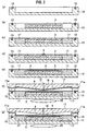
Fig. 2] Figs. 2 (a) to 2 (g ) are diagrams illustrating steps of a seed crystal fixing method. - [
Fig. 3] Fig. 3 is a schematic sectional view of an apparatus (crucible) for manufacturing a silicon carbide single crystal. - A seed crystal fixing device 1 of the present invention will be described in detail below with reference to the drawings.
-
Fig. 1(a) shows a schematic sectional view of the seed crystal fixing device 1 holding a seedcrystal placing part 3 on which aseed crystal 9 is placed with an adhesive 5 interposed in between.Fig. 1(b) shows a top plan view of an upper chamber.Fig. 1(c) shows a top plan view of a lower chamber. - As shown in
Fig. 1(a) , in the seed crystal fixing device 1 of this embodiment, theseed crystal 9 is fixed to the seedcrystal placing part 3 of a reaction vessel with theadhesive 5 interposed in between. The seed crystal fixing device 1 includes achamber 10 and a flexiblepouched body 16. The seedcrystal placing part 3 can be placed inside thechamber 10, and thechamber 10 can form a hermetic atmosphere. The flexiblepouched body 16 is placed on the upper surface of the inside of thechamber 10. The flexiblepouched body 16 can be inflated with a delivering of gas, and can be deflated with an exhaust of the gas. When inflated, the flexiblepouched body 16 contacts with a surface of theseed crystal 9, and applies a uniform pressure to the entire surface of theseed crystal 9. The upper surface of the inside of thechamber 10 forms convex shape towards the seedcrystal placing part 3. The seed crystal fixing device 1 also includes aheater 20 that heats and hardens the adhesive. - The flexible
pouched body 16 is made of either a rubber or a resin. As shown inFig. 1(a) , the flexiblepouched body 16 is fixed inside thechamber 10 by being clamped atsidewall portions 11a of theupper chamber 11. - The
chamber 10 includes theupper chamber 11 and thelower chamber 13, which can be assembled together and separated from each other freely. When thechamber 10 is used, theupper chamber 11 is fitted to thelower chamber 13 with an O-ring 15 installed in an outer-peripheral portion of thelower chamber 13. Thechamber 10 can form a hermetic atmosphere accordingly. A gas-inlet/outlet port (gas-delivery/exhaust port) 12 is formed substantially at the central position of theupper chamber 11. The seed crystal fixing device 1 can form a reduced-pressure atmosphere inside thechamber 10 by taking out air from the inside of thechamber 10 where a hermetic atmosphere is formed. - As shown in
Fig. 1(b) , the gas-inlet/outlet port 12 is formed substantially at the central position of theupper chamber 11. In theupper chamber 11,grooves 11b extended radially from the central position of the gas-inlet/outlet port 12. When the flexiblepouched body 16 is inflated, thegrooves 11b allow the air exhausted through the gas-inlet/outlet port 12 to disperse uniformly within the flexiblepouched body 16. With this configuration, the air exhausted through the gas-inlet/outlet port 12 inflates firstly the central portion of the flexiblepouched body 16 located right above the seedcrystal placing part 3 and then inflates the peripheral portion of the flexiblepouched body 16. Accordingly, the flexiblepouched body 16 presses firstly the substantially central portion of theseed crystal 9 and then the peripheral portion of theseed crystal 9. - As shown in
Figs. 1(a) and 1(c) , thelower chamber 13 includes a ring-shaped guide portion 17, which is provided to fix the seedcrystal placing part 3 and to fix theseed crystal 9. After the seedcrystal placing part 3 is installed in thelower chamber 13, theguide portion 17 is detachably fixed to thelower chamber 13 and then theseed crystal 9 is mounted on top of the seedcrystal placing part 3. Note that this way of fixing the seedcrystal placing part 3 is not the only way. Alternatively, the seedcrystal placing part 3 may be fixed by fitting the seedcrystal placing part 3 into a hole dug in the chamber. - As an example of the seed
crystal placing part 3 installed in the seed crystal fixing device 1, a seedcrystal placing part 3 of a silicon carbide singlecrystal manufacturing apparatus 30 which will be described later and which is shown inFig. 3 can be used. Although it depends on the purpose of use, as theseed crystal 9, a 6H-Lely crystal, a 6H-Acheson crystal and the like can be used. As the adhesive 5, resins, carbohydrates, and heat-resistant fine particles are enumerated. Some examples of the resins that can be used are thermosetting resins such as phenol resins, novolac resins, and furfuryl-alcohol resins. Alternatively, a mixture of a phenol resin with carbon powder can also be used. Some examples of the carbohydrates are sugars, specifically, monosaccharides such as glucose, polysaccharides such as cellulose, and derivatives of these monosaccharides and polysaccharides. Some examples of the heat-resistant fine particles are graphite (carbon), heat-resistant substances such as silicon carbide (SiC) and boron nitride (BN), high-melting-point metals such as tungsten and tantalum, and compounds of these metals such as carbides of these metals and nitrides of these metals. - A method of fixing a seed crystal according to an embodiment using the seed crystal fixing apparatus shown in
Fig. 1 will be described with reference toFigs. 2(a) to 2(g) . - (i) Firstly, the
lower chamber 13 is prepared as shown inFig. 2(a) . - (ii) Next, the seed
crystal placing part 3 of the reaction vessel is placed in thelower chamber 13 as shown inFig. 2(b) . - (iii) Then, the seed
crystal placing part 3 is fixed by theguide portion 17 as shown inFig. 2(c) . - (iv) The adhesive 5 is applied to the top of the seed
crystal placing part 3 as shown inFig. 2 (d) . The amount of the applied adhesive 5 preferably ranges from 1 µl/cm2 to 25 µl/cm2. - (v) Subsequently, as shown in
Fig. 2(e) , theseed crystal 9 is mounted on top of the seedcrystal placing part 3 with the applied adhesive 5 interposed in between. For the purpose of improving the adhesiveness of theseed crystal 9 to the seedcrystal placing part 3, it is preferable that the contact surface of theseed crystal 9 with the seedcrystal placing part 3 be polished. Specifically, the surface roughness (Ra) of the contact surface of theseed crystal 9 is preferably equal to or smaller than 0.1 µm. In addition, it is preferable that the surface of the seedcrystal placing part 3 on which theseed crystal 9 is mounted have a surface roughness equal to or smaller than 1.4 µm because such a low surface roughness contributes to an improvement in the adhesiveness. - (vi) As shown in
Fig. 2(f) , a hermetic atmosphere is formed by mounting theupper chamber 11 on thelower chamber 13. - (vii) As shown in
Fig. 2(g) , the flexiblepouched body 16 is inflated by delivering gas through the gas-inlet/outlet port 12. Note that the inflating of the flexiblepouched body 16 starts from the substantially central position of the flexiblepouched body 16. Accordingly, the inflated flexiblepouched body 16 presses firstly the substantially central portion of theseed crystal 9 located right below the substantially central position of the flexiblepouched body 16. Subsequently, when the entire flexiblepouched body 16 is inflated, the flexiblepouched body 16 presses eventually theentire seed crystal 9. The flexiblepouched body 16 is brought into contact with a surface of theseed crystal 9 on a side opposite to the seed-crystal mounting surface, and thus a uniform pressure is applied to the entire surface of theseed crystal 9. It is preferable that a load of a pressure ranging from 0.01 MPa to 1 MPa, approximately, be applied to theseed crystal 9. - (viii) The adhesive 5 is hardened by being heated with a
heater 20. The conditions for the heating vary depending upon the properties of the adhesive (thermosetting resin). The adhesive 5 is to be heated at a temperature ranging from 100°C to 1000°C, or more preferably from 100°C to 300°C, for approximately 5 minutes to 10 minutes. - Note that if gas, which is produced when the adhesive 5 is hardened remains between the
seed crystal 9 and the seedcrystal placing part 3 as bubbles, the bubbles may possibly cause ununiform bonding. Accordingly, it is preferable that thermal hardening process of the adhesive 5 is performed under a reduced-pressure atmosphere while the air and the gas that may possibly cause the ununiform bonding are sucked out from thechamber 10 by a suction apparatus (not illustrated) connected to the gas-inlet/outlet port 12. When the reduced-pressure atmosphere is formed, the reduced-pressure atmosphere should be formed before the above-described step (vii). Performing the steps (vii) and (viii) after the formation of the reduced-pressure atmosphere contributes an effect of improving the uniformity of the pressure loaded on theseed crystal 9. In addition, the bonding under the same conditions at anytime helps to replicate the bonding state with more certainty. It is preferable that the reduced-pressure atmosphere be not higher than 300 Torr. Following the above-described procedure, theseed crystal 9 is fixed to the top of the seedcrystal placing part 3. - Descriptions have been given thus far as to the seed crystal fixing method and the like. However, a silicon carbide single crystal manufacturing method is also provided as another embodiment of the present invention. Specifically, what is provided is a silicon carbide single crystal manufacturing method including: placing a sublimation raw material in a reaction vessel to accommodate the sublimation raw material; mounting a seed crystal facing substantially the sublimation raw material; and recrystallizing the sublimed sublimation raw material on the seed crystal, so that a silicon carbide single crystal is grown. In the provided method, the single crystal is grown on the seed crystal that is fixed to the top of the seed crystal placing part by the seed crystal fixing method of the above-described embodiment.
- A silicon carbide single
crystal manufacturing apparatus 30 is used as the reaction vessel as shown inFig. 3 . The silicon carbide singlecrystal manufacturing apparatus 30 includes: avessel 31 capable of accommodating a sublimationraw material 35; and the seedcrystal placing part 3 detachably attached to thevessel 31 and capable of mounting theseed crystal 9 thereon.First induction coils 33a and second induction coils 33b are provided around the outer circumference of the reaction vessel to form a silicon carbide sublimation atmosphere. There is no special limitation on thevessel 31 as long as the silicon carbide sublimation atmosphere can be formed inside thevessel 31. For example, a crucible can be used as thevessel 31, and a preferable material for thevessel 31 is graphite. It is more preferable that thevessel 31 be made of a material with a thermal expansion coefficient that is substantially the same as that of the seed crystal. For facilitating the putting of the sublimationraw material 35 in thevessel 31, it is preferable that thevessel 31 and the seedcrystal placing part 3 be formed together and the seedcrystal placing part 3 be detachably attached to thevessel 31. As means of joining thevessel 31 and seedcrystal placing part 3 together, any means can be employed as long as the inside of thevessel 31 can be kept in a sealed-up state. An example of such joining means is screwing means. - As the sublimation
raw material 35, various conventionally known materials can be used. An example of the sublimationraw material 35 is a silicon carbide powder obtained by heating and baking, under an argon atmosphere, a mixture obtained by mixing uniformly a highly pure tetraethoxysilane polymer used as the silicon source and a resol-type phenolic resin used as the carbon source. In addition, as a seed crystal of the silicon carbide single crystal, a conventionally known single crystal can be used. - There is no special limitation on the heating conditions, such as the heating temperature, under which the sublimation
raw material 35 is heated. The heating conditions can be set up by those skilled in the art based on a known technique. - The silicon carbide single crystal is manufactured according to the above-described silicon carbide single crystal manufacturing method. It is preferable that the silicon carbide single crystal has crystal defects (tubular defects) of 50 defects/cm2 or less, preferably 10 defects/cm2 or less when the single crystal is evaluated by etching with a molten alkali. The total content of metal impurity elements in the silicon carbide single crystal is preferably 10 ppm or less. Since the silicon carbide single crystal obtained in the invention has a quite high quality without mingling of polycrystals and polymorphic crystals and without crystal defects such as micro-pipes, it is excellent in dielectric breakdown resistance, heat resistance and radiation resistance, and may be favorably used for electronic devices such as semiconductor wafers and optical devices such as light emission diodes.
- According to the aforementioned method for producing the silicon carbide single crystal of the invention, a high quality silicon carbide single crystal can be readily and efficiently produced without causing damages such as cracks.
- Various embodiments of the invention made by the inventors have been described thus far, but the present invention is not limited to any of the descriptions and the drawings, of these embodiments, that form parts of the disclosure of the present invention. To put it differently, if those skilled in the art, based on the above-described embodiments, conceive of other embodiments, examples, and operating techniques, all of these must be included in the scope of the present invention.
- According to the seed crystal fixing apparatus of the present invention, the upper surface of the chamber forms convex shape towards the seed crystal placing part. Accordingly, when the flexible pouched body is inflated, the substantially central portion of the seed crystal mounted on top of the seed crystal placing part is firstly brought into contact with the flexible pouched body and uniform press-bonding across the entire surface of the seed crystal can be accomplished.
Claims (3)
- A seed crystal fixing device for fixing a seed crystal to a seed crystal placing part with an adhesive interposed in between, the seed crystal fixing device comprising:a chamber capable of installing the seed crystal placing part in the inside thereof; anda flexible pouched body placed on an upper surface of the chamber, the flexible pouched body is inflated with a delivery of gas and is deflated with an exhaust of the gas, the flexible pouched body contacts with a surface of the seed crystal when inflated, thereby applying pressure uniformly across the entire surface of the seed crystal,wherein the upper surface of the chamber forms convex shape towards the seed crystal placing part.
- The seed crystal fixing device according to claim 1, wherein a groove is formed in the upper surface of the chamber.
- The seed crystal fixing device according to claim 1, wherein a gas delivery/exhaust port towards the flexible pouched body is formed at a central portion in the upper surface of the chamber.
Applications Claiming Priority (2)
| Application Number | Priority Date | Filing Date | Title |
|---|---|---|---|
| JP2006271711A JP5081423B2 (en) | 2006-10-03 | 2006-10-03 | Seed crystal fixing device |
| PCT/JP2007/069390 WO2008041728A1 (en) | 2006-10-03 | 2007-10-03 | Seed crystal fixing device |
Publications (3)
| Publication Number | Publication Date |
|---|---|
| EP2071061A1 true EP2071061A1 (en) | 2009-06-17 |
| EP2071061A4 EP2071061A4 (en) | 2010-05-19 |
| EP2071061B1 EP2071061B1 (en) | 2012-02-08 |
Family
ID=39268582
Family Applications (1)
| Application Number | Title | Priority Date | Filing Date |
|---|---|---|---|
| EP07829129A Not-in-force EP2071061B1 (en) | 2006-10-03 | 2007-10-03 | Seed crystal fixing device |
Country Status (5)
| Country | Link |
|---|---|
| US (1) | US8051888B2 (en) |
| EP (1) | EP2071061B1 (en) |
| JP (1) | JP5081423B2 (en) |
| AT (1) | ATE544885T1 (en) |
| WO (1) | WO2008041728A1 (en) |
Families Citing this family (2)
| Publication number | Priority date | Publication date | Assignee | Title |
|---|---|---|---|---|
| JP4998491B2 (en) * | 2009-02-20 | 2012-08-15 | トヨタ自動車株式会社 | Method for bonding SiC single crystal and solution growing method for SiC single crystal |
| CN116377596B (en) * | 2023-06-06 | 2023-10-13 | 苏州优晶光电科技有限公司 | Heating device and heating method for bonding and fixing silicon carbide seed crystal |
Family Cites Families (7)
| Publication number | Priority date | Publication date | Assignee | Title |
|---|---|---|---|---|
| JP3680531B2 (en) * | 1997-12-11 | 2005-08-10 | 株式会社豊田中央研究所 | Seed crystal fixing agent and method for producing single crystal using the same |
| JP4258921B2 (en) * | 1999-11-10 | 2009-04-30 | 株式会社豊田中央研究所 | Seed crystal fixing agent, seed crystal fixing method, and method for producing single crystal using them |
| JP4224755B2 (en) * | 2001-10-16 | 2009-02-18 | 株式会社デンソー | Seed crystal fixation method |
| US7601441B2 (en) * | 2002-06-24 | 2009-10-13 | Cree, Inc. | One hundred millimeter high purity semi-insulating single crystal silicon carbide wafer |
| JP4401649B2 (en) * | 2002-12-13 | 2010-01-20 | キヤノン株式会社 | Manufacturing method of solar cell module |
| JP4501657B2 (en) * | 2004-11-30 | 2010-07-14 | パナソニック株式会社 | Seed crystal fixing method for silicon carbide single crystal growth |
| US7497906B2 (en) * | 2006-03-08 | 2009-03-03 | Bridgestone Corporation | Seed crystal fixing apparatus and a method for fixing the seed crystal |
-
2006
- 2006-10-03 JP JP2006271711A patent/JP5081423B2/en not_active Expired - Fee Related
-
2007
- 2007-10-03 AT AT07829129T patent/ATE544885T1/en active
- 2007-10-03 EP EP07829129A patent/EP2071061B1/en not_active Not-in-force
- 2007-10-03 WO PCT/JP2007/069390 patent/WO2008041728A1/en not_active Ceased
- 2007-10-03 US US12/444,105 patent/US8051888B2/en not_active Expired - Fee Related
Also Published As
| Publication number | Publication date |
|---|---|
| EP2071061A4 (en) | 2010-05-19 |
| US20100065223A1 (en) | 2010-03-18 |
| EP2071061B1 (en) | 2012-02-08 |
| ATE544885T1 (en) | 2012-02-15 |
| JP2008088024A (en) | 2008-04-17 |
| WO2008041728A1 (en) | 2008-04-10 |
| US8051888B2 (en) | 2011-11-08 |
| JP5081423B2 (en) | 2012-11-28 |
Similar Documents
| Publication | Publication Date | Title |
|---|---|---|
| EP2508653B1 (en) | Method for producing monocrystal | |
| EP2072646A1 (en) | Process for producing single crystal of silicon carbide | |
| KR101504772B1 (en) | A method for growing aluminum nitride crystals, a method for producing aluminum nitride crystals, | |
| US20090269490A1 (en) | Coating apparatus and coating method | |
| US7497906B2 (en) | Seed crystal fixing apparatus and a method for fixing the seed crystal | |
| JP2020066571A (en) | Method for producing seed crystal including protective film, method for producing ingot using the same, seed crystal including protective film, and method for attaching seed crystal | |
| WO2000039372A1 (en) | Method for growing single crystal of silicon carbide | |
| EP3763853A1 (en) | Production method for silicon carbide single crystal | |
| JP4556634B2 (en) | Seed crystal fixing part and seed crystal fixing method | |
| US20110229719A1 (en) | Manufacturing method for crystal, manufacturing apparatus for crystal, and stacked film | |
| US20210301420A1 (en) | Production method of silicon carbide wafer, production method of semiconductor substrate, and production method of silicon carbide semiconductor device | |
| JP4523733B2 (en) | Method for producing silicon carbide single crystal ingot and method for mounting seed crystal for growing silicon carbide single crystal | |
| JP4599816B2 (en) | Manufacturing method of silicon epitaxial wafer | |
| US8051888B2 (en) | Seed crystal fixing device | |
| KR20210021469A (en) | Silicon carbide single crystal growth device and silicon carbide single crystal manufacturing method | |
| EP2267195B1 (en) | Method for producing silicon carbide single crystal | |
| JP2000226299A (en) | Method for producing single-crystal silicon carbide thin film and single-crystal silicon carbide thin film | |
| JP5030440B2 (en) | Seed crystal fixing device and seed crystal fixing method | |
| JP2006347868A (en) | Apparatus and method of fixing seed crystal | |
| EP3767014A1 (en) | Production method of silicon carbide single crystal | |
| JP3876488B2 (en) | Method for producing silicon carbide single crystal | |
| JP5336307B2 (en) | Method for producing silicon carbide single crystal | |
| JP2010083681A (en) | Production method of silicon carbide single crystal and vacuum chuck | |
| CN117965117A (en) | Adhesive, method for bonding silicon carbide seed crystal, silicon carbide crystal and growth method thereof | |
| JP4457708B2 (en) | Seed crystal fixing method and single crystal manufacturing method |
Legal Events
| Date | Code | Title | Description |
|---|---|---|---|
| PUAI | Public reference made under article 153(3) epc to a published international application that has entered the european phase |
Free format text: ORIGINAL CODE: 0009012 |
|
| 17P | Request for examination filed |
Effective date: 20090407 |
|
| AK | Designated contracting states |
Kind code of ref document: A1 Designated state(s): AT BE BG CH CY CZ DE DK EE ES FI FR GB GR HU IE IS IT LI LT LU LV MC MT NL PL PT RO SE SI SK TR |
|
| AX | Request for extension of the european patent |
Extension state: AL BA HR MK RS |
|
| A4 | Supplementary search report drawn up and despatched |
Effective date: 20100416 |
|
| RIC1 | Information provided on ipc code assigned before grant |
Ipc: C30B 29/36 20060101ALI20100412BHEP Ipc: C30B 23/00 20060101AFI20080506BHEP |
|
| RIC1 | Information provided on ipc code assigned before grant |
Ipc: C30B 23/00 20060101AFI20110530BHEP Ipc: C30B 29/36 20060101ALI20110530BHEP |
|
| GRAP | Despatch of communication of intention to grant a patent |
Free format text: ORIGINAL CODE: EPIDOSNIGR1 |
|
| DAX | Request for extension of the european patent (deleted) | ||
| GRAS | Grant fee paid |
Free format text: ORIGINAL CODE: EPIDOSNIGR3 |
|
| GRAA | (expected) grant |
Free format text: ORIGINAL CODE: 0009210 |
|
| AK | Designated contracting states |
Kind code of ref document: B1 Designated state(s): AT BE BG CH CY CZ DE DK EE ES FI FR GB GR HU IE IS IT LI LT LU LV MC MT NL PL PT RO SE SI SK TR |
|
| REG | Reference to a national code |
Ref country code: GB Ref legal event code: FG4D |
|
| REG | Reference to a national code |
Ref country code: AT Ref legal event code: REF Ref document number: 544885 Country of ref document: AT Kind code of ref document: T Effective date: 20120215 Ref country code: CH Ref legal event code: EP |
|
| REG | Reference to a national code |
Ref country code: DE Ref legal event code: R096 Ref document number: 602007020613 Country of ref document: DE Effective date: 20120405 |
|
| REG | Reference to a national code |
Ref country code: NL Ref legal event code: VDEP Effective date: 20120208 |
|
| LTIE | Lt: invalidation of european patent or patent extension |
Effective date: 20120208 |
|
| PG25 | Lapsed in a contracting state [announced via postgrant information from national office to epo] |
Ref country code: LT Free format text: LAPSE BECAUSE OF FAILURE TO SUBMIT A TRANSLATION OF THE DESCRIPTION OR TO PAY THE FEE WITHIN THE PRESCRIBED TIME-LIMIT Effective date: 20120208 Ref country code: IS Free format text: LAPSE BECAUSE OF FAILURE TO SUBMIT A TRANSLATION OF THE DESCRIPTION OR TO PAY THE FEE WITHIN THE PRESCRIBED TIME-LIMIT Effective date: 20120608 Ref country code: NL Free format text: LAPSE BECAUSE OF FAILURE TO SUBMIT A TRANSLATION OF THE DESCRIPTION OR TO PAY THE FEE WITHIN THE PRESCRIBED TIME-LIMIT Effective date: 20120208 |
|
| PG25 | Lapsed in a contracting state [announced via postgrant information from national office to epo] |
Ref country code: LV Free format text: LAPSE BECAUSE OF FAILURE TO SUBMIT A TRANSLATION OF THE DESCRIPTION OR TO PAY THE FEE WITHIN THE PRESCRIBED TIME-LIMIT Effective date: 20120208 Ref country code: PL Free format text: LAPSE BECAUSE OF FAILURE TO SUBMIT A TRANSLATION OF THE DESCRIPTION OR TO PAY THE FEE WITHIN THE PRESCRIBED TIME-LIMIT Effective date: 20120208 Ref country code: GR Free format text: LAPSE BECAUSE OF FAILURE TO SUBMIT A TRANSLATION OF THE DESCRIPTION OR TO PAY THE FEE WITHIN THE PRESCRIBED TIME-LIMIT Effective date: 20120509 Ref country code: BE Free format text: LAPSE BECAUSE OF FAILURE TO SUBMIT A TRANSLATION OF THE DESCRIPTION OR TO PAY THE FEE WITHIN THE PRESCRIBED TIME-LIMIT Effective date: 20120208 Ref country code: FI Free format text: LAPSE BECAUSE OF FAILURE TO SUBMIT A TRANSLATION OF THE DESCRIPTION OR TO PAY THE FEE WITHIN THE PRESCRIBED TIME-LIMIT Effective date: 20120208 Ref country code: PT Free format text: LAPSE BECAUSE OF FAILURE TO SUBMIT A TRANSLATION OF THE DESCRIPTION OR TO PAY THE FEE WITHIN THE PRESCRIBED TIME-LIMIT Effective date: 20120608 |
|
| REG | Reference to a national code |
Ref country code: AT Ref legal event code: MK05 Ref document number: 544885 Country of ref document: AT Kind code of ref document: T Effective date: 20120208 |
|
| PG25 | Lapsed in a contracting state [announced via postgrant information from national office to epo] |
Ref country code: CY Free format text: LAPSE BECAUSE OF FAILURE TO SUBMIT A TRANSLATION OF THE DESCRIPTION OR TO PAY THE FEE WITHIN THE PRESCRIBED TIME-LIMIT Effective date: 20120208 |
|
| PG25 | Lapsed in a contracting state [announced via postgrant information from national office to epo] |
Ref country code: EE Free format text: LAPSE BECAUSE OF FAILURE TO SUBMIT A TRANSLATION OF THE DESCRIPTION OR TO PAY THE FEE WITHIN THE PRESCRIBED TIME-LIMIT Effective date: 20120208 Ref country code: CZ Free format text: LAPSE BECAUSE OF FAILURE TO SUBMIT A TRANSLATION OF THE DESCRIPTION OR TO PAY THE FEE WITHIN THE PRESCRIBED TIME-LIMIT Effective date: 20120208 Ref country code: SI Free format text: LAPSE BECAUSE OF FAILURE TO SUBMIT A TRANSLATION OF THE DESCRIPTION OR TO PAY THE FEE WITHIN THE PRESCRIBED TIME-LIMIT Effective date: 20120208 Ref country code: DK Free format text: LAPSE BECAUSE OF FAILURE TO SUBMIT A TRANSLATION OF THE DESCRIPTION OR TO PAY THE FEE WITHIN THE PRESCRIBED TIME-LIMIT Effective date: 20120208 Ref country code: SE Free format text: LAPSE BECAUSE OF FAILURE TO SUBMIT A TRANSLATION OF THE DESCRIPTION OR TO PAY THE FEE WITHIN THE PRESCRIBED TIME-LIMIT Effective date: 20120208 Ref country code: RO Free format text: LAPSE BECAUSE OF FAILURE TO SUBMIT A TRANSLATION OF THE DESCRIPTION OR TO PAY THE FEE WITHIN THE PRESCRIBED TIME-LIMIT Effective date: 20120208 |
|
| PG25 | Lapsed in a contracting state [announced via postgrant information from national office to epo] |
Ref country code: SK Free format text: LAPSE BECAUSE OF FAILURE TO SUBMIT A TRANSLATION OF THE DESCRIPTION OR TO PAY THE FEE WITHIN THE PRESCRIBED TIME-LIMIT Effective date: 20120208 Ref country code: IT Free format text: LAPSE BECAUSE OF FAILURE TO SUBMIT A TRANSLATION OF THE DESCRIPTION OR TO PAY THE FEE WITHIN THE PRESCRIBED TIME-LIMIT Effective date: 20120208 |
|
| PLBE | No opposition filed within time limit |
Free format text: ORIGINAL CODE: 0009261 |
|
| STAA | Information on the status of an ep patent application or granted ep patent |
Free format text: STATUS: NO OPPOSITION FILED WITHIN TIME LIMIT |
|
| 26N | No opposition filed |
Effective date: 20121109 |
|
| PG25 | Lapsed in a contracting state [announced via postgrant information from national office to epo] |
Ref country code: AT Free format text: LAPSE BECAUSE OF FAILURE TO SUBMIT A TRANSLATION OF THE DESCRIPTION OR TO PAY THE FEE WITHIN THE PRESCRIBED TIME-LIMIT Effective date: 20120208 |
|
| REG | Reference to a national code |
Ref country code: DE Ref legal event code: R097 Ref document number: 602007020613 Country of ref document: DE Effective date: 20121109 |
|
| PG25 | Lapsed in a contracting state [announced via postgrant information from national office to epo] |
Ref country code: ES Free format text: LAPSE BECAUSE OF FAILURE TO SUBMIT A TRANSLATION OF THE DESCRIPTION OR TO PAY THE FEE WITHIN THE PRESCRIBED TIME-LIMIT Effective date: 20120519 |
|
| PG25 | Lapsed in a contracting state [announced via postgrant information from national office to epo] |
Ref country code: MC Free format text: LAPSE BECAUSE OF NON-PAYMENT OF DUE FEES Effective date: 20121031 |
|
| REG | Reference to a national code |
Ref country code: CH Ref legal event code: PL |
|
| GBPC | Gb: european patent ceased through non-payment of renewal fee |
Effective date: 20121003 |
|
| REG | Reference to a national code |
Ref country code: IE Ref legal event code: MM4A |
|
| REG | Reference to a national code |
Ref country code: FR Ref legal event code: ST Effective date: 20130628 |
|
| PG25 | Lapsed in a contracting state [announced via postgrant information from national office to epo] |
Ref country code: IE Free format text: LAPSE BECAUSE OF NON-PAYMENT OF DUE FEES Effective date: 20121003 Ref country code: GB Free format text: LAPSE BECAUSE OF NON-PAYMENT OF DUE FEES Effective date: 20121003 Ref country code: BG Free format text: LAPSE BECAUSE OF FAILURE TO SUBMIT A TRANSLATION OF THE DESCRIPTION OR TO PAY THE FEE WITHIN THE PRESCRIBED TIME-LIMIT Effective date: 20120508 Ref country code: CH Free format text: LAPSE BECAUSE OF NON-PAYMENT OF DUE FEES Effective date: 20121031 Ref country code: LI Free format text: LAPSE BECAUSE OF NON-PAYMENT OF DUE FEES Effective date: 20121031 |
|
| PG25 | Lapsed in a contracting state [announced via postgrant information from national office to epo] |
Ref country code: FR Free format text: LAPSE BECAUSE OF NON-PAYMENT OF DUE FEES Effective date: 20121031 |
|
| PG25 | Lapsed in a contracting state [announced via postgrant information from national office to epo] |
Ref country code: MT Free format text: LAPSE BECAUSE OF FAILURE TO SUBMIT A TRANSLATION OF THE DESCRIPTION OR TO PAY THE FEE WITHIN THE PRESCRIBED TIME-LIMIT Effective date: 20120208 |
|
| PGFP | Annual fee paid to national office [announced via postgrant information from national office to epo] |
Ref country code: DE Payment date: 20131021 Year of fee payment: 7 |
|
| PG25 | Lapsed in a contracting state [announced via postgrant information from national office to epo] |
Ref country code: TR Free format text: LAPSE BECAUSE OF FAILURE TO SUBMIT A TRANSLATION OF THE DESCRIPTION OR TO PAY THE FEE WITHIN THE PRESCRIBED TIME-LIMIT Effective date: 20120208 |
|
| PG25 | Lapsed in a contracting state [announced via postgrant information from national office to epo] |
Ref country code: LU Free format text: LAPSE BECAUSE OF NON-PAYMENT OF DUE FEES Effective date: 20121003 |
|
| PG25 | Lapsed in a contracting state [announced via postgrant information from national office to epo] |
Ref country code: HU Free format text: LAPSE BECAUSE OF FAILURE TO SUBMIT A TRANSLATION OF THE DESCRIPTION OR TO PAY THE FEE WITHIN THE PRESCRIBED TIME-LIMIT Effective date: 20071003 |
|
| REG | Reference to a national code |
Ref country code: DE Ref legal event code: R082 Ref document number: 602007020613 Country of ref document: DE Representative=s name: MARKS & CLERK (LUXEMBOURG) LLP, LU |
|
| REG | Reference to a national code |
Ref country code: DE Ref legal event code: R082 Ref document number: 602007020613 Country of ref document: DE Representative=s name: MARKS & CLERK (LUXEMBOURG) LLP, LU Effective date: 20140828 Ref country code: DE Ref legal event code: R081 Ref document number: 602007020613 Country of ref document: DE Owner name: BRIDGESTONE CORPORATION, JP Free format text: FORMER OWNER: BRIDGESTONE CORP., TOKIO/TOKYO, JP Effective date: 20140828 |
|
| REG | Reference to a national code |
Ref country code: DE Ref legal event code: R119 Ref document number: 602007020613 Country of ref document: DE |
|
| PG25 | Lapsed in a contracting state [announced via postgrant information from national office to epo] |
Ref country code: DE Free format text: LAPSE BECAUSE OF NON-PAYMENT OF DUE FEES Effective date: 20150501 |