EP2068249A1 - Detection system for peripheral device - Google Patents
Detection system for peripheral device Download PDFInfo
- Publication number
- EP2068249A1 EP2068249A1 EP08167405A EP08167405A EP2068249A1 EP 2068249 A1 EP2068249 A1 EP 2068249A1 EP 08167405 A EP08167405 A EP 08167405A EP 08167405 A EP08167405 A EP 08167405A EP 2068249 A1 EP2068249 A1 EP 2068249A1
- Authority
- EP
- European Patent Office
- Prior art keywords
- peripheral device
- mainboard
- detection system
- measuring pin
- slot
- Prior art date
- Legal status (The legal status is an assumption and is not a legal conclusion. Google has not performed a legal analysis and makes no representation as to the accuracy of the status listed.)
- Withdrawn
Links
Images


Classifications
-
- G—PHYSICS
- G06—COMPUTING OR CALCULATING; COUNTING
- G06F—ELECTRIC DIGITAL DATA PROCESSING
- G06F13/00—Interconnection of, or transfer of information or other signals between, memories, input/output devices or central processing units
- G06F13/38—Information transfer, e.g. on bus
- G06F13/40—Bus structure
- G06F13/4063—Device-to-bus coupling
- G06F13/409—Mechanical coupling
Definitions
- the present invention relates to a detection system for a peripheral device, and more particularly to a system for detecting whether each peripheral device of a personal computer (PC) is completely inserted in a corresponding peripheral device slot of a mainboard before power-on.
- PC personal computer
- PCI peripheral component interface
- SATA Serial ATA
- the user may buy an SATA-PCI peripheral device to expand the function of the mainboard to support SATA.
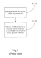
- a flow chart of a conventional insertion test is shown.
- the installation process is divided into two steps.
- a peripheral device is inserted after the PC is powered off (Step S110).
- the PC is powered on to see whether the peripheral device operates normally (Step S120).
- the user cannot know immediately whether the peripheral device is correctly inserted in the PCI expansion slot, and may only determine the insertion state of the peripheral device by observing whether a basic input output system (BIOS) or an operating system is connected to the peripheral device after power-on. Therefore, such test is not only time and energy consuming, but also may cause damages to the peripheral device due to insertion errors. As a result, it is inconvenient for the user on installation and also increases the maintenance cost for the manufacturer.
- BIOS basic input output system
- the present invention is mainly directed to a detection system for a peripheral device, so as to detect whether the peripheral device is correctly inserted in a corresponding peripheral device slot of a mainboard before power-on.
- a detection system for a peripheral device which includes a power supply unit, a logic component, and a detecting unit.
- the power supply unit After the mainboard is booted, the power supply unit provides a first power for the mainboard and the peripheral device to operate, and when the mainboard is shut down, the power supply unit provides a second power for the mainboard to remain in a minimum operation.
- An input end of the logic component is electrically connected to a first measuring pin and a second measuring pin of the peripheral device slot respectively, and the first and second measuring pins are further respectively corresponding to a ground pin of the peripheral device.
- the logic component When the peripheral device is inserted in the peripheral device slot, the logic component outputs a determination output value according to the potentials of the first and second measuring pins.
- the detecting unit is electrically connected to an output pin of the logic component, for determining whether each peripheral device is inserted in the corresponding peripheral device slot according to the determination output value. In addition, on detecting that the peripheral device is not completely inserted in the peripheral device slot before power-on, the detecting unit stops the boot program of the mainboard and sends out an alarm signal.
- a detection system for a peripheral device for determining whether a peripheral device is completely inserted in a peripheral device slot of a mainboard before power-on according to the change in the potential of a first and a second measuring pin of the peripheral device.
- the detecting unit On detecting that the peripheral device is not completely inserted in the peripheral device slot before power-on, the detecting unit sends a control signal to the mainboard, and the mainboard sends an alarm signal to inform the user. Meanwhile, the boot program of the mainboard is stopped to prevent damages to the mainboard and the peripheral device due to installation errors of the peripheral device.
- a detection system for a peripheral device for detecting a peripheral device of a PC, so as to make sure whether the peripheral device is correctly inserted in a corresponding peripheral device slot of a mainboard before power-on.
- the PC at least includes a mainboard 210, a power supply unit 220, a peripheral device 230, a peripheral device slot 240, and a detection system 250.
- the interface of the peripheral device 230 is one corresponding to a central process unit (CPU) or a memory, or is an accelerated graphics port (AGP) interface, a PCI interface, a PCI-E interface, an SATA interface, or an integrated device electronics (IDE) interface.
- CPU central process unit
- AGP accelerated graphics port
- the detection system 250 includes a logic component 251, a switching switch 252, and a detecting unit 253.
- the power supply unit 220 follows the Advanced Technology extend (ATX) power supply standard.
- the ATX not only specifies the power supply voltage for the operation of the mainboard 210, but also describes the basic power supply for the peripheral device 230 when shut-down.
- the ATX provides the following different voltages: "+3.3 V”, “+5 V”, “+12 V”, “-12 V”, “-5 V”, and "+5 V Stand-By”. For instance, "+12 V” is used to drive a disc drive motor and a cooling fan when the mainboard 210 is booted, or to drive the peripheral device 230 through the peripheral device slot 240 of the mainboard 210.
- the mainboard 210 is provided with a BIOS.
- the BIOS may be stored in an electrically erasable programmable read-only memory (EEPROM) or other flash memories, and used for managing the operating procedure of the mainboard 210.
- EEPROM electrically erasable programmable read-only memory
- the power supply unit 220 provides a first power for the mainboard 210 and the peripheral device 230 to operate, and when the mainboard 210 is shut down, the power supply unit 220 provides a second power for the mainboard 210 to remain in a standby operation.
- the second power provided when the mainboard 210 is shut down is adopted as the power for performing the detection.
- An input end of the logic component 251 is electrically connected to a first measuring pin and a second measuring pin of the peripheral device slot 240 respectively.
- the first and second measuring pins are further respectively corresponding to a ground pin of the peripheral device 230.
- the detecting unit 253 is electrically connected to an output pin of the logic component 251, for determining whether each peripheral device 230 is inserted in the corresponding peripheral device slot 240 according to the determination output value. In addition, on detecting that the peripheral device 230 is not completely inserted in the peripheral device slot 240 before power-on, the detecting unit 253 stops the boot program of the BIOS and sends out an alarm signal.
- the first and second measuring pins of the peripheral device slot 240 are both at a high potential. It should be noted that, when the peripheral device 230 is completely inserted in the peripheral device slot 240, the first and second measuring pins are electrically connected to the ground pin of the peripheral device respectively, such that the potential of the first measuring pin changes from a high potential to a low potential, and the potential of the second measuring pin changes from a high potential to a low potential. Therefore, when the detecting unit 253 detects that the first and second measuring pins are both at a low potential, it indicates that the peripheral device 230 is truly inserted in the peripheral device slot 240.
- Circumstances that the peripheral device 230 is not completely inserted in the peripheral device slot 240 are shown below.
- the first circumstance is that, as the peripheral device 230 is not truly inserted in the peripheral device slot 240, the first and second measuring pins are not connected to the peripheral device 230, such that the first and second measuring pins both remain at a high potential.
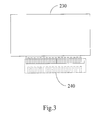
- FIG. 3 a schematic view of a false installation of the peripheral device is shown.
- the second and third circumstances are that, as an end of the peripheral device 230 is not truly inserted in the peripheral device slot 240, the first and second measuring pins may have different voltages.
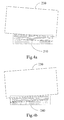
- FIGs. 4a and 4b schematic views of various false installations of the peripheral device are shown respectively. For example, if only the first measuring pin is connected to the peripheral device 230, the potential of the first measuring pin changes into a low potential, and meanwhile, if the second measuring pin is not connected to the peripheral device 230, the second measuring pin still remains at a high potential.
- the change of the potential in the above circumstances is input into the logic component 251, and the logic component 251 thus outputs a corresponding determination output value.
- the logic component 251 determines through a NOR gate.
- An input end of the NOR gate is electrically connected to the first and second measuring pins respectively, and an output end of the NOR gate is connected to a testing unit.
- FIG. 5 a schematic architectural view of the present invention using a NOR gate is shown. The following results listed in Table 1 are obtained after the potential output from the first and second measuring pins passes through the NOR gate.
- Table 1 Truth Table for NOR Gate First Measuring Pin Second Measuring Pin Output End 0 0 1 0 1 0 1 0 0 0 1 1 0
- the detecting unit 253 stops the boot program of the BIOS, and sends an alarm signal to the user.
- the alarm signal may be sent by a loudspeaker or a light-emitting diode (LED), so as to inform the user that the peripheral device 230 fails to be completely inserted.
- the user can check whether the peripheral device 230 is completely inserted in the peripheral device slot 240 according to the alarm signal. As such, it is ensured that the peripheral device 230 is completely inserted in the peripheral device slot 240, and the mainboard 210 is then booted to supply power to the peripheral device 230.
- the switching switch 252 is electrically connected between the logic component 251 and the detecting unit 253, and is used for determining whether the peripheral device 230 needs to be detected by the detecting unit 253.
- the switching switch 252 is, for example, a dip switch.
- the switching switch 252 may be a hardware, or a related function set in the BIOS for determining whether the peripheral device 230 needs to be tested. Referring to FIG. 6 , a schematic view of the present invention detecting peripheral devices with a dip switch is shown.
- the switching switch 252 in FIGs. 5 and 6 is respectively corresponding to the peripheral device slots 240 of different logic component devices 251.
- the user may disable the peripheral device slot 240 via the switching switch 252, such that the detecting unit 253 will skip the test on the peripheral device slot 240.
- the mainboard 210 both has a built-in display function and a display card slot, and the built-in display is taken by the user as a preset value when the system is booted, the test on the display card slot may be disabled, so as to shorten the detection time before the system is booted.
- a detection system 250 for a peripheral device 230 is provided to determine whether the peripheral device 230 is completely inserted in a peripheral device slot 240 before power-on according to the change in the potentials of a first and a second measuring pin of the peripheral device 230.
- the detecting unit 253 On detecting that the peripheral device 230 is not completely inserted in the peripheral device slot 240, the detecting unit 253 sends a control signal to a mainboard 210, and the mainboard 210 sends an alarm signal to inform the user. Meanwhile, the boot program of the mainboard 210 is stopped to prevent damages to the mainboard 210 and the peripheral device 230 due to installation errors of the peripheral device 230.
Landscapes
- Engineering & Computer Science (AREA)
- General Engineering & Computer Science (AREA)
- Theoretical Computer Science (AREA)
- Computer Hardware Design (AREA)
- Physics & Mathematics (AREA)
- General Physics & Mathematics (AREA)
- Power Sources (AREA)
- Test And Diagnosis Of Digital Computers (AREA)
- Debugging And Monitoring (AREA)
Abstract
Description
- The present invention relates to a detection system for a peripheral device, and more particularly to a system for detecting whether each peripheral device of a personal computer (PC) is completely inserted in a corresponding peripheral device slot of a mainboard before power-on.
- Usually the function of a PC is expanded through various peripheral devices. Taking a PC for example, generally, its mainboard is provided with peripheral component interface (PCI) expansion slots. Thus, a user can buy corresponding PCI peripheral devices to expand the function of the mainboard.
- For example, if the user intends to install a Serial ATA (SATA) hard disk drive, while the mainboard does not provide a corresponding interface, the user may buy an SATA-PCI peripheral device to expand the function of the mainboard to support SATA.
- Referring to
FIG. 1 , a flow chart of a conventional insertion test is shown. Generally, the installation process is divided into two steps. First, a peripheral device is inserted after the PC is powered off (Step S110). After the peripheral device is inserted, the PC is powered on to see whether the peripheral device operates normally (Step S120). However, the user cannot know immediately whether the peripheral device is correctly inserted in the PCI expansion slot, and may only determine the insertion state of the peripheral device by observing whether a basic input output system (BIOS) or an operating system is connected to the peripheral device after power-on. Therefore, such test is not only time and energy consuming, but also may cause damages to the peripheral device due to insertion errors. As a result, it is inconvenient for the user on installation and also increases the maintenance cost for the manufacturer. - Accordingly, the present invention is mainly directed to a detection system for a peripheral device, so as to detect whether the peripheral device is correctly inserted in a corresponding peripheral device slot of a mainboard before power-on.
- In order to achieve the above objective, a detection system for a peripheral device is provided, which includes a power supply unit, a logic component, and a detecting unit. After the mainboard is booted, the power supply unit provides a first power for the mainboard and the peripheral device to operate, and when the mainboard is shut down, the power supply unit provides a second power for the mainboard to remain in a minimum operation. An input end of the logic component is electrically connected to a first measuring pin and a second measuring pin of the peripheral device slot respectively, and the first and second measuring pins are further respectively corresponding to a ground pin of the peripheral device. When the peripheral device is inserted in the peripheral device slot, the logic component outputs a determination output value according to the potentials of the first and second measuring pins. The detecting unit is electrically connected to an output pin of the logic component, for determining whether each peripheral device is inserted in the corresponding peripheral device slot according to the determination output value. In addition, on detecting that the peripheral device is not completely inserted in the peripheral device slot before power-on, the detecting unit stops the boot program of the mainboard and sends out an alarm signal.
- A detection system for a peripheral device is provided, for determining whether a peripheral device is completely inserted in a peripheral device slot of a mainboard before power-on according to the change in the potential of a first and a second measuring pin of the peripheral device. On detecting that the peripheral device is not completely inserted in the peripheral device slot before power-on, the detecting unit sends a control signal to the mainboard, and the mainboard sends an alarm signal to inform the user. Meanwhile, the boot program of the mainboard is stopped to prevent damages to the mainboard and the peripheral device due to installation errors of the peripheral device.
- The present invention will become more fully understood from the detailed description given herein below for illustration only, and thus are not limitative of the present invention, and wherein:
-
FIG. 1 is a flow chart of a conventional insertion test; -
FIG. 2 is a schematic architectural view of the present invention; -
FIG. 3 is a schematic view of a false installation of a peripheral device; -
FIG. 4a is a schematic view of a false installation of a peripheral device; -
FIG. 4b is a schematic view of a false installation of a peripheral device; -
FIG. 5 is a schematic architectural view of the present invention using a NOR gate; and -
FIG. 6 is a schematic view of the present invention detecting peripheral devices using a dip switch. - A detection system for a peripheral device is provided for detecting a peripheral device of a PC, so as to make sure whether the peripheral device is correctly inserted in a corresponding peripheral device slot of a mainboard before power-on. In a preferred embodiment of the present invention, taking a PC for example, the PC at least includes a
mainboard 210, apower supply unit 220, aperipheral device 230, aperipheral device slot 240, and adetection system 250. The interface of theperipheral device 230 is one corresponding to a central process unit (CPU) or a memory, or is an accelerated graphics port (AGP) interface, a PCI interface, a PCI-E interface, an SATA interface, or an integrated device electronics (IDE) interface. - The
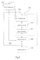
detection system 250 includes alogic component 251, aswitching switch 252, and a detectingunit 253. Referring toFIG. 2 , a schematic architectural view of the present invention is shown. In the present invention, thepower supply unit 220 follows the Advanced Technology extend (ATX) power supply standard. The ATX not only specifies the power supply voltage for the operation of themainboard 210, but also describes the basic power supply for theperipheral device 230 when shut-down. The ATX provides the following different voltages: "+3.3 V", "+5 V", "+12 V", "-12 V", "-5 V", and "+5 V Stand-By". For instance, "+12 V" is used to drive a disc drive motor and a cooling fan when themainboard 210 is booted, or to drive theperipheral device 230 through theperipheral device slot 240 of themainboard 210. - Generally, the
mainboard 210 is provided with a BIOS. The BIOS may be stored in an electrically erasable programmable read-only memory (EEPROM) or other flash memories, and used for managing the operating procedure of themainboard 210. After themainboard 210 is booted, thepower supply unit 220 provides a first power for themainboard 210 and theperipheral device 230 to operate, and when themainboard 210 is shut down, thepower supply unit 220 provides a second power for themainboard 210 to remain in a standby operation. In the present invention, the second power provided when themainboard 210 is shut down is adopted as the power for performing the detection. - An input end of the
logic component 251 is electrically connected to a first measuring pin and a second measuring pin of theperipheral device slot 240 respectively. In addition, the first and second measuring pins are further respectively corresponding to a ground pin of theperipheral device 230. When theperipheral device 230 is inserted in theperipheral device slot 240, thelogic component 251 outputs a determination output value according to the potentials of the first and second measuring pins. - The detecting
unit 253 is electrically connected to an output pin of thelogic component 251, for determining whether eachperipheral device 230 is inserted in the correspondingperipheral device slot 240 according to the determination output value. In addition, on detecting that theperipheral device 230 is not completely inserted in theperipheral device slot 240 before power-on, the detectingunit 253 stops the boot program of the BIOS and sends out an alarm signal. - In the present invention, if the
peripheral device 230 is not inserted in theperipheral device slot 240, the first and second measuring pins of theperipheral device slot 240 are both at a high potential. It should be noted that, when theperipheral device 230 is completely inserted in theperipheral device slot 240, the first and second measuring pins are electrically connected to the ground pin of the peripheral device respectively, such that the potential of the first measuring pin changes from a high potential to a low potential, and the potential of the second measuring pin changes from a high potential to a low potential. Therefore, when the detectingunit 253 detects that the first and second measuring pins are both at a low potential, it indicates that theperipheral device 230 is truly inserted in theperipheral device slot 240. - Circumstances that the
peripheral device 230 is not completely inserted in theperipheral device slot 240 are shown below. The first circumstance is that, as theperipheral device 230 is not truly inserted in theperipheral device slot 240, the first and second measuring pins are not connected to theperipheral device 230, such that the first and second measuring pins both remain at a high potential. Referring toFIG. 3 , a schematic view of a false installation of the peripheral device is shown. - The second and third circumstances are that, as an end of the
peripheral device 230 is not truly inserted in theperipheral device slot 240, the first and second measuring pins may have different voltages. Referring toFIGs. 4a and 4b , schematic views of various false installations of the peripheral device are shown respectively. For example, if only the first measuring pin is connected to theperipheral device 230, the potential of the first measuring pin changes into a low potential, and meanwhile, if the second measuring pin is not connected to theperipheral device 230, the second measuring pin still remains at a high potential. - It should be noted that, the change of the potential in the above circumstances is input into the
logic component 251, and thelogic component 251 thus outputs a corresponding determination output value. In addition, thelogic component 251 determines through a NOR gate. - An input end of the NOR gate is electrically connected to the first and second measuring pins respectively, and an output end of the NOR gate is connected to a testing unit. Referring to
FIG. 5 , a schematic architectural view of the present invention using a NOR gate is shown. The following results listed in Table 1 are obtained after the potential output from the first and second measuring pins passes through the NOR gate.Table 1 Truth Table for NOR Gate First Measuring Pin Second Measuring Pin Output End 0 0 1 0 1 0 1 0 0 1 1 0 - In Table 1, "1" represents a high potential, and "0" represents a low potential. When the first measuring pin or the second measuring pin is at a low potential, the NOR gate outputs "0", and thus the detecting
unit 253 determines that theperipheral device 230 is not completely inserted in theperipheral device slot 240. If the first and second measuring pins are both "0", the output end outputs "1", and thus the detectingunit 253 ensures that theperipheral device 230 is completely inserted in theperipheral device slot 240. When the first and second measuring pins are both at a high potential, the output end outputs "0", and thus the detectingunit 253 determines that theperipheral device 230 is not inserted in theperipheral device slot 240. - If the
peripheral device 230 is not completely inserted in theperipheral device slot 240, the detectingunit 253 stops the boot program of the BIOS, and sends an alarm signal to the user. The alarm signal may be sent by a loudspeaker or a light-emitting diode (LED), so as to inform the user that theperipheral device 230 fails to be completely inserted. Thereby, the user can check whether theperipheral device 230 is completely inserted in theperipheral device slot 240 according to the alarm signal. As such, it is ensured that theperipheral device 230 is completely inserted in theperipheral device slot 240, and themainboard 210 is then booted to supply power to theperipheral device 230. - The switching
switch 252 is electrically connected between thelogic component 251 and the detectingunit 253, and is used for determining whether theperipheral device 230 needs to be detected by the detectingunit 253. The switchingswitch 252 is, for example, a dip switch. In addition, the switchingswitch 252 may be a hardware, or a related function set in the BIOS for determining whether theperipheral device 230 needs to be tested. Referring toFIG. 6 , a schematic view of the present invention detecting peripheral devices with a dip switch is shown. - The switching
switch 252 inFIGs. 5 and6 is respectively corresponding to theperipheral device slots 240 of differentlogic component devices 251. On determining that someperipheral device slot 240 does not need to be tested, the user may disable theperipheral device slot 240 via the switchingswitch 252, such that the detectingunit 253 will skip the test on theperipheral device slot 240. For example, if themainboard 210 both has a built-in display function and a display card slot, and the built-in display is taken by the user as a preset value when the system is booted, the test on the display card slot may be disabled, so as to shorten the detection time before the system is booted. - In view of the above, a
detection system 250 for aperipheral device 230 is provided to determine whether theperipheral device 230 is completely inserted in aperipheral device slot 240 before power-on according to the change in the potentials of a first and a second measuring pin of theperipheral device 230. On detecting that theperipheral device 230 is not completely inserted in theperipheral device slot 240, the detectingunit 253 sends a control signal to amainboard 210, and themainboard 210 sends an alarm signal to inform the user. Meanwhile, the boot program of themainboard 210 is stopped to prevent damages to themainboard 210 and theperipheral device 230 due to installation errors of theperipheral device 230.
Claims (7)
- A detection system for a peripheral device, for detecting whether the peripheral device is correctly inserted in a corresponding peripheral device slot of a mainboard before power-on, the detection system comprising:a logic component, wherein an input end of the logic component is electrically connected to a first measuring pin and a second measuring pin of the peripheral device slot respectively, the first measuring pin and the second measuring pin are further respectively corresponding to a ground pin of the peripheral device, and when the peripheral device is inserted in the peripheral device slot, the logic component outputs a determination output value according to the potentials of the first measuring pin and the second measuring pin; anda detecting unit, electrically connected to an output pin of the logic component, for determining whether each peripheral device is inserted in the corresponding peripheral device slot according to the determination output value, wherein on detecting that the peripheral device is not completely inserted in the peripheral device slot before power-on, the detecting unit stops a boot program of the mainboard and sends out an alarm signal.
- The detection system for a peripheral device as claimed in claim 1, further comprising a power supply unit electrically connected to the peripheral devices, wherein after the mainboard is booted, the power supply unit provides a first power for the mainboard and the peripheral devices to operate, and when the mainboard is shut down, the power supply unit provides a second power for the mainboard to remain in a standby operation.
- The detection system for a peripheral device as claimed in claim 1, wherein when the peripheral device is completely inserted in the peripheral device slot, the first measuring pin and the second measuring pin are electrically connected to the ground pin of the peripheral device respectively, such that the potential of the first measuring pin changes from a high potential to a low potential, and the potential of the second measuring pin changes from a high potential to a low potential.
- The detection system for a peripheral device as claimed in claim 1, wherein the logic component is an EXCLUSIVE NOR gate, an input end of the EXCLUSIVE NOR gate is electrically connected to the first measuring pin and the second measuring pin respectively, and an output end of the EXCLUSIVE NOR gate is connected to the detecting unit.
- The detection system for a peripheral device as claimed in claim 1, wherein the mainboard further has a basic input output system (BIOS), for managing operating procedures of the mainboard.
- The detection system for a peripheral device as claimed in claim 5, wherein if the detecting unit detects that the peripheral device is not completely inserted in the peripheral device slot before power-on, the BIOS switches the power supply unit to provide the second power for the mainboard to operate.
- The detection system for a peripheral device as claimed in claim 1, further comprising a switching switch, for determining whether the peripheral devices need to be detected by the detecting unit.
Applications Claiming Priority (1)
| Application Number | Priority Date | Filing Date | Title |
|---|---|---|---|
| TW096145804A TW200923658A (en) | 2007-11-30 | 2007-11-30 | Detection system for the peripheral apparatus |
Publications (1)
| Publication Number | Publication Date |
|---|---|
| EP2068249A1 true EP2068249A1 (en) | 2009-06-10 |
Family
ID=40456893
Family Applications (1)
| Application Number | Title | Priority Date | Filing Date |
|---|---|---|---|
| EP08167405A Withdrawn EP2068249A1 (en) | 2007-11-30 | 2008-10-23 | Detection system for peripheral device |
Country Status (4)
| Country | Link |
|---|---|
| US (1) | US7849234B2 (en) |
| EP (1) | EP2068249A1 (en) |
| JP (1) | JP2009134705A (en) |
| TW (1) | TW200923658A (en) |
Cited By (1)
| Publication number | Priority date | Publication date | Assignee | Title |
|---|---|---|---|---|
| CN103970247B (en) * | 2013-02-01 | 2017-03-01 | 技嘉科技股份有限公司 | Mainboard and power supply control method thereof |
Families Citing this family (10)
| Publication number | Priority date | Publication date | Assignee | Title |
|---|---|---|---|---|
| BRPI1004997A2 (en) * | 2009-11-11 | 2013-02-26 | Seiko Epson Corp | electronic device and control method |
| KR101629709B1 (en) * | 2010-01-20 | 2016-06-14 | 삼성전자주식회사 | Apparatus and method for booting in computer device with a built-in communication module |
| WO2011090486A1 (en) | 2010-01-22 | 2011-07-28 | Hewlett-Packard Development Company, L.P. | I/o control systems and methods |
| EP2365445B1 (en) * | 2010-03-11 | 2013-10-23 | Ricoh Company, Ltd. | Adapter and communication method |
| TWI440840B (en) * | 2011-09-08 | 2014-06-11 | Inventec Corp | Shock test device |
| US20140258699A1 (en) * | 2013-03-07 | 2014-09-11 | Aspeed Technology Inc. | Boot fault tolerant device and method thereof |
| CN104659585A (en) * | 2013-11-22 | 2015-05-27 | 鸿富锦精密工业(深圳)有限公司 | Electric arc suppression device |
| TWI623834B (en) * | 2015-03-25 | 2018-05-11 | 環鴻科技股份有限公司 | Booting method for computer system |
| TWI689812B (en) * | 2018-11-30 | 2020-04-01 | 英業達股份有限公司 | Method of locating the location of an error of a memory device |
| TWI746154B (en) * | 2020-09-08 | 2021-11-11 | 宏碁股份有限公司 | Computer device and method for increasing stability of computer device |
Citations (4)
| Publication number | Priority date | Publication date | Assignee | Title |
|---|---|---|---|---|
| US5805903A (en) * | 1996-05-21 | 1998-09-08 | Compaq Computer Corporation | Protection of computer system against incorrect card insertion during start-up |
| EP0996061A2 (en) * | 1998-10-20 | 2000-04-26 | Fujitsu Limited | Error handling method |
| US6789149B1 (en) | 2000-01-25 | 2004-09-07 | Dell Products L.P. | Scheme to detect correct plug-in function modules in computers |
| US7155552B1 (en) * | 2004-09-27 | 2006-12-26 | Emc Corporation | Apparatus and method for highly available module insertion |
Family Cites Families (5)
| Publication number | Priority date | Publication date | Assignee | Title |
|---|---|---|---|---|
| US5922060A (en) * | 1996-12-31 | 1999-07-13 | Compaq Computer Corporation | Expansion card insertion and removal |
| US6393586B1 (en) * | 1999-02-04 | 2002-05-21 | Dell Usa, L.P. | Method and apparatus for diagnosing and conveying an identification code in post on a non-booting personal computer |
| WO2002089081A1 (en) * | 2001-04-26 | 2002-11-07 | Caveo Technology, Llc | Pc card security system |
| US7860582B2 (en) * | 2004-06-23 | 2010-12-28 | National Instruments Corporation | Compact modular embedded device |
| US8099124B2 (en) * | 2007-04-12 | 2012-01-17 | Symbol Technologies, Inc. | Method and system for correlating user/device activity with spatial orientation sensors |
-
2007
- 2007-11-30 TW TW096145804A patent/TW200923658A/en not_active IP Right Cessation
-
2008
- 2008-06-02 US US12/155,297 patent/US7849234B2/en active Active
- 2008-10-23 EP EP08167405A patent/EP2068249A1/en not_active Withdrawn
- 2008-10-30 JP JP2008279687A patent/JP2009134705A/en active Pending
Patent Citations (4)
| Publication number | Priority date | Publication date | Assignee | Title |
|---|---|---|---|---|
| US5805903A (en) * | 1996-05-21 | 1998-09-08 | Compaq Computer Corporation | Protection of computer system against incorrect card insertion during start-up |
| EP0996061A2 (en) * | 1998-10-20 | 2000-04-26 | Fujitsu Limited | Error handling method |
| US6789149B1 (en) | 2000-01-25 | 2004-09-07 | Dell Products L.P. | Scheme to detect correct plug-in function modules in computers |
| US7155552B1 (en) * | 2004-09-27 | 2006-12-26 | Emc Corporation | Apparatus and method for highly available module insertion |
Cited By (1)
| Publication number | Priority date | Publication date | Assignee | Title |
|---|---|---|---|---|
| CN103970247B (en) * | 2013-02-01 | 2017-03-01 | 技嘉科技股份有限公司 | Mainboard and power supply control method thereof |
Also Published As
| Publication number | Publication date |
|---|---|
| US20090144460A1 (en) | 2009-06-04 |
| JP2009134705A (en) | 2009-06-18 |
| TW200923658A (en) | 2009-06-01 |
| TWI351611B (en) | 2011-11-01 |
| US7849234B2 (en) | 2010-12-07 |
Similar Documents
| Publication | Publication Date | Title |
|---|---|---|
| CN101436154B (en) | Computer motherboard startup and shutdown test system and method | |
| JP2009134705A (en) | Detection system for peripheral device | |
| US20100306592A1 (en) | Computer system on and off test apparatus and method | |
| US20140195697A1 (en) | Apparatus and method for detecting functions of video card | |
| US20110246138A1 (en) | Hardware status detecting circuit for generating one hardware status detecting signal having information of multiple hardware status detectors, related hardware status identifying circuit, related hardware status detecting system, and related methods | |
| US20130318389A1 (en) | Power supply management system and method | |
| US20170211839A1 (en) | Back-up power source apparatus in indoor unit, controlling method thereof and multi-split air conditioning system | |
| CN104572226A (en) | Method and device for detecting mainboard starting abnormity | |
| CN103995760A (en) | Computer fault detection device and detection and maintenance method | |
| TW201512831A (en) | Computer booting system and method of a computer | |
| CN103605591A (en) | Method and device for controlling memory initialization of terminal system | |
| CN113366576A (en) | Retention self-test for power loss operations on memory systems | |
| TWI534707B (en) | Computer system, shutdown and boot method thereof | |
| US9158646B2 (en) | Abnormal information output system for a computer system | |
| US9021242B2 (en) | Boot determining method of electronic device having one or more storage disks in a low temperature environment | |
| US20070168738A1 (en) | Power-on error detection system and method | |
| US7213159B2 (en) | Method for testing and verifying power management features of computer system | |
| US20130138939A1 (en) | Method for processing booting errors | |
| US7900030B2 (en) | Method for determining a rebooting action of a computer system and related computer system | |
| CN104731686A (en) | Indicator control system and electronic device | |
| CN107239372A (en) | Electronic device and detection method thereof | |
| KR20090037223A (en) | System and method for performing self-diagnosis after shutdown and booting method using it | |
| CN104794042A (en) | Computer detecting system and method | |
| CN102855166A (en) | Mainboard testing system and method | |
| WO2012039711A1 (en) | Method and system for performing system maintenance in a computing device |
Legal Events
| Date | Code | Title | Description |
|---|---|---|---|
| PUAI | Public reference made under article 153(3) epc to a published international application that has entered the european phase |
Free format text: ORIGINAL CODE: 0009012 |
|
| AK | Designated contracting states |
Kind code of ref document: A1 Designated state(s): AT BE BG CH CY CZ DE DK EE ES FI FR GB GR HR HU IE IS IT LI LT LU LV MC MT NL NO PL PT RO SE SI SK TR |
|
| AX | Request for extension of the european patent |
Extension state: AL BA MK RS |
|
| 17P | Request for examination filed |
Effective date: 20090910 |
|
| AKX | Designation fees paid |
Designated state(s): DE FR GB |
|
| 17Q | First examination report despatched |
Effective date: 20110209 |
|
| STAA | Information on the status of an ep patent application or granted ep patent |
Free format text: STATUS: THE APPLICATION IS DEEMED TO BE WITHDRAWN |
|
| 18D | Application deemed to be withdrawn |
Effective date: 20110621 |