EP2066019A2 - Voltage clamping and energy recovery circuits - Google Patents
Voltage clamping and energy recovery circuits Download PDFInfo
- Publication number
- EP2066019A2 EP2066019A2 EP08020685A EP08020685A EP2066019A2 EP 2066019 A2 EP2066019 A2 EP 2066019A2 EP 08020685 A EP08020685 A EP 08020685A EP 08020685 A EP08020685 A EP 08020685A EP 2066019 A2 EP2066019 A2 EP 2066019A2
- Authority
- EP
- European Patent Office
- Prior art keywords
- line
- main
- circuit
- auxiliary
- capacitor
- Prior art date
- Legal status (The legal status is an assumption and is not a legal conclusion. Google has not performed a legal analysis and makes no representation as to the accuracy of the status listed.)
- Granted
Links
- 238000011084 recovery Methods 0.000 title claims abstract description 37
- 239000003990 capacitor Substances 0.000 claims abstract description 100
- 239000004065 semiconductor Substances 0.000 claims abstract description 72
- 230000008878 coupling Effects 0.000 claims abstract description 53
- 238000010168 coupling process Methods 0.000 claims abstract description 53
- 238000005859 coupling reaction Methods 0.000 claims abstract description 53
- 238000004804 winding Methods 0.000 claims abstract description 39
- 230000002441 reversible effect Effects 0.000 claims abstract description 24
- 230000000903 blocking effect Effects 0.000 claims abstract description 18
- 101100449816 Saccharomyces cerevisiae (strain ATCC 204508 / S288c) GTO1 gene Proteins 0.000 claims abstract description 17
- 238000007599 discharging Methods 0.000 claims abstract description 17
- 101100449818 Saccharomyces cerevisiae (strain ATCC 204508 / S288c) ECM4 gene Proteins 0.000 claims abstract 3
- 101100449817 Schizosaccharomyces pombe (strain 972 / ATCC 24843) gto2 gene Proteins 0.000 claims abstract 3
- 238000000034 method Methods 0.000 claims description 20
- 101100365087 Arabidopsis thaliana SCRA gene Proteins 0.000 claims description 12
- 101150105073 SCR1 gene Proteins 0.000 claims description 12
- 101100134054 Saccharomyces cerevisiae (strain ATCC 204508 / S288c) NTG1 gene Proteins 0.000 claims description 12
- NEEVCWPRIZJJRJ-LWRDCAMISA-N 5-(benzylideneamino)-6-[(e)-benzylideneamino]-2-sulfanylidene-1h-pyrimidin-4-one Chemical compound C=1C=CC=CC=1C=NC=1C(=O)NC(=S)NC=1\N=C\C1=CC=CC=C1 NEEVCWPRIZJJRJ-LWRDCAMISA-N 0.000 claims description 5
- 238000012544 monitoring process Methods 0.000 claims description 3
- 102100020865 EKC/KEOPS complex subunit LAGE3 Human genes 0.000 abstract description 13
- 101001137983 Homo sapiens EKC/KEOPS complex subunit LAGE3 Proteins 0.000 abstract description 13
- MOJZMWJRUKIQGL-XILRTYJMSA-N procyanidin C1 Chemical compound C1([C@@H]2[C@H](O)[C@H](C3=C(O)C=C(O)C=C3O2)C2=C3O[C@@H]([C@H](O)[C@H](C3=C(O)C=C2O)C=2C(O)=CC(O)=C3C[C@H]([C@H](OC3=2)C=2C=C(O)C(O)=CC=2)O)C=2C=C(O)C(O)=CC=2)=CC=C(O)C(O)=C1 MOJZMWJRUKIQGL-XILRTYJMSA-N 0.000 abstract description 13
- 101100449819 Saccharomyces cerevisiae (strain ATCC 204508 / S288c) GTO3 gene Proteins 0.000 abstract description 2
- 101100122529 Saccharomyces cerevisiae (strain ATCC 204508 / S288c) GON7 gene Proteins 0.000 description 10
- 238000010586 diagram Methods 0.000 description 9
- 230000008569 process Effects 0.000 description 9
- 230000008901 benefit Effects 0.000 description 5
- 230000008859 change Effects 0.000 description 5
- 230000000694 effects Effects 0.000 description 5
- 230000009471 action Effects 0.000 description 4
- 238000010304 firing Methods 0.000 description 4
- 101000668165 Homo sapiens RNA-binding motif, single-stranded-interacting protein 1 Proteins 0.000 description 3
- 102100039692 RNA-binding motif, single-stranded-interacting protein 1 Human genes 0.000 description 3
- 230000003071 parasitic effect Effects 0.000 description 2
- 101000668170 Homo sapiens RNA-binding motif, single-stranded-interacting protein 2 Proteins 0.000 description 1
- 102100039690 RNA-binding motif, single-stranded-interacting protein 2 Human genes 0.000 description 1
- 238000012790 confirmation Methods 0.000 description 1
- 230000003111 delayed effect Effects 0.000 description 1
- 230000001419 dependent effect Effects 0.000 description 1
- 230000005284 excitation Effects 0.000 description 1
- 230000004907 flux Effects 0.000 description 1
- 230000006698 induction Effects 0.000 description 1
- 239000011159 matrix material Substances 0.000 description 1
- 230000000737 periodic effect Effects 0.000 description 1
- 238000005086 pumping Methods 0.000 description 1
- 230000001172 regenerating effect Effects 0.000 description 1
- 230000001360 synchronised effect Effects 0.000 description 1
Images


Classifications
-
- H—ELECTRICITY
- H02—GENERATION; CONVERSION OR DISTRIBUTION OF ELECTRIC POWER
- H02K—DYNAMO-ELECTRIC MACHINES
- H02K29/00—Motors or generators having non-mechanical commutating devices, e.g. discharge tubes or semiconductor devices
-
- H—ELECTRICITY
- H02—GENERATION; CONVERSION OR DISTRIBUTION OF ELECTRIC POWER
- H02P—CONTROL OR REGULATION OF ELECTRIC MOTORS, ELECTRIC GENERATORS OR DYNAMO-ELECTRIC CONVERTERS; CONTROLLING TRANSFORMERS, REACTORS OR CHOKE COILS
- H02P25/00—Arrangements or methods for the control of AC motors characterised by the kind of AC motor or by structural details
- H02P25/02—Arrangements or methods for the control of AC motors characterised by the kind of AC motor or by structural details characterised by the kind of motor
- H02P25/022—Synchronous motors
- H02P25/024—Synchronous motors controlled by supply frequency
-
- H—ELECTRICITY
- H02—GENERATION; CONVERSION OR DISTRIBUTION OF ELECTRIC POWER
- H02M—APPARATUS FOR CONVERSION BETWEEN AC AND AC, BETWEEN AC AND DC, OR BETWEEN DC AND DC, AND FOR USE WITH MAINS OR SIMILAR POWER SUPPLY SYSTEMS; CONVERSION OF DC OR AC INPUT POWER INTO SURGE OUTPUT POWER; CONTROL OR REGULATION THEREOF
- H02M1/00—Details of apparatus for conversion
-
- H—ELECTRICITY
- H02—GENERATION; CONVERSION OR DISTRIBUTION OF ELECTRIC POWER
- H02M—APPARATUS FOR CONVERSION BETWEEN AC AND AC, BETWEEN AC AND DC, OR BETWEEN DC AND DC, AND FOR USE WITH MAINS OR SIMILAR POWER SUPPLY SYSTEMS; CONVERSION OF DC OR AC INPUT POWER INTO SURGE OUTPUT POWER; CONTROL OR REGULATION THEREOF
- H02M3/00—Conversion of dc power input into dc power output
- H02M3/22—Conversion of dc power input into dc power output with intermediate conversion into ac
- H02M3/24—Conversion of dc power input into dc power output with intermediate conversion into ac by static converters
- H02M3/28—Conversion of dc power input into dc power output with intermediate conversion into ac by static converters using discharge tubes with control electrode or semiconductor devices with control electrode to produce the intermediate ac
- H02M3/325—Conversion of dc power input into dc power output with intermediate conversion into ac by static converters using discharge tubes with control electrode or semiconductor devices with control electrode to produce the intermediate ac using devices of a triode or a transistor type requiring continuous application of a control signal
- H02M3/335—Conversion of dc power input into dc power output with intermediate conversion into ac by static converters using discharge tubes with control electrode or semiconductor devices with control electrode to produce the intermediate ac using devices of a triode or a transistor type requiring continuous application of a control signal using semiconductor devices only
-
- H—ELECTRICITY
- H02—GENERATION; CONVERSION OR DISTRIBUTION OF ELECTRIC POWER
- H02P—CONTROL OR REGULATION OF ELECTRIC MOTORS, ELECTRIC GENERATORS OR DYNAMO-ELECTRIC CONVERTERS; CONTROLLING TRANSFORMERS, REACTORS OR CHOKE COILS
- H02P6/00—Arrangements for controlling synchronous motors or other dynamo-electric motors using electronic commutation dependent on the rotor position; Electronic commutators therefor
- H02P6/14—Electronic commutators
Definitions
- the present invention relates to voltage clamping and energy recovery circuits, and in particular to circuits for recovering energy that would otherwise be dissipated as heat in a switching aid network (snubber) during a forced commutation process where an outgoing semiconductor switching device of an electronic commutator circuit is commutated entirely by gate control.
- a switching aid network switching aid network
- British Patent Application 2433360 discloses an electronic commutator circuit for use with a stator winding of an electrical machine.
- the stator winding includes a number of coils linked by the same number of points of common coupling.
- the electronic commutator circuit includes the same number of switching stages with each switching stage being connected between a respective one of the points of common coupling and first and second dc lines.
- Each switching stage includes a first reverse blocking semiconductor power device capable of being turned on and off by gate control having its anode connected to the first dc line and a second reverse blocking semiconductor power device capable of being turned on and off by gate control having its cathode connected to the second dc line.
- a preferred type of semiconductor power device is the Reverse Blocking Gate Turn Off Thyristor (RB-GTO) or RB-GTO derivative because they benefit from reduced on-state losses relative to other gate commutated device families such as Insulated Gate Bipolar Transistors (IGBTs) as a result of their internal regenerative properties.
- RB-GTO Reverse Blocking Gate Turn Off Thyristor
- IGBTs Insulated Gate Bipolar Transistors
- the reverse blocking semiconductor power devices are used in place of conventional thyristors and this means that the electronic commutation circuit can force the commutation of current irrespective of the voltage in the stator winding.
- the electric commutator circuit may also include a switching aid network (snubber) connected in parallel with each of the semiconductor power devices.
- the snubber may be a series connected resistor-capacitor or configured according to the well known industry standard "RCD Polarised Snubber" as shown in the figures of British Patent Application 2433360 .
- the purpose of either type of snubber is to assist the forced commutation process and reducing switching losses in the power semiconductor devices.
- the dissipation of energy within the snubber when the outgoing RB-GTO is switched during a forced commutation process represents an appreciable energy loss and reduces the overall efficiency of the electronic commutator circuit.
- the present invention provides a way of recovering the energy that would otherwise be dissipated within the switching aid network (snubber) and returning it to another part of the electrical system or dissipating it elsewhere where the heat can be more easily managed. More particularly, the present invention provides a circuit for use with a stator winding of an electrical machine, the stator winding including a number of coils linked by the same number of points of common coupling, the circuit comprising:
- An advantage of the present invention is that the first and second capacitors of the voltage clamping circuit are shared by all of the individual clamping stages.
- the diodes of the clamping stages effectively replace the switching aid network and snubber components of a conventional electronic commutator circuit.
- the voltage clamping and energy recovery circuit of the present invention therefore has relatively few electrical components, which means lower hardware costs and improved reliability.
- the first and second capacitors can be selectively discharged (preferably through an essentially lossless discharge path) to any suitable part of the electrical system associated with the electrical machine or to another part of the system.
- the means for selectively discharging the first and second capacitors is preferably an energy recovery circuit for recovering the energy stored in the first and second capacitors. It is generally preferred that the energy recovery circuit includes a dc to dc converter means for selectively discharging the first capacitor to one of the first and second main dc lines and selectively discharging the second capacitor to the other of the first and second main dc lines.
- the first capacitor arranged between the first main dc line and the first auxiliary dc line may be selectively discharged to the first main dc line or the second main dc line depending on the dc voltage polarity.
- the voltage clamping circuit may further include a third capacitor connected between the first and second auxiliary dc lines.
- the voltage clamping circuit may further include a plurality of first capacitors connected between the first main dc line and the first auxiliary dc line and a plurality of second capacitors connected between the second main dc line and the second auxiliary dc line.
- the circuit will usually include first and second dc terminals; the first dc terminal being connected to the first main dc line and the second dc terminal being connected to the second main dc line.
- the circuit will preferably include a series connected thyristor and resistor connected between the first and second dc terminals.
- the dc to dc converter means may include a first semiconductor power device and a first inductor connected in series between the first auxiliary dc line and the second main dc line, a second semiconductor power device and a second inductor connected in series between the second auxiliary dc line and the first main dc line, and a third semiconductor power device having its cathode connected to a junction between the first semiconductor power device and the first inductor and its anode connected to a junction between the second semiconductor power device and the second inductor.
- the anode of the first semiconductor power device of the dc to dc converter means is preferably connected to the first auxiliary dc line and the cathode of the second semiconductor power device of the dc to dc converter means is preferably connected to the second auxiliary dc line.
- the dc to dc converter means may include a first semiconductor power device and a first inductor connected in series between the first auxiliary dc line and the first main dc line, a second semiconductor power device and a second inductor connected in series between the second auxiliary dc line and the second main dc line, and a third semiconductor power device having its cathode connected to a junction between the first semiconductor power device and the first inductor and its anode connected to a junction between the second semiconductor power device and the second inductor.
- the anode of the first semiconductor power device of the dc to dc converter means is preferably connected to the first auxiliary dc line and the cathode of the second semiconductor power device of the dc to dc converter means is preferably connected to the second auxiliary dc line.
- the third semiconductor power device of the first and second arrangements of the dc to dc converter means may be a diode or a thyristor depending on the intended operating modes of the electrical machine. For example, if the electrical machine is designed to operate in a motoring mode only then the third semiconductor power device will normally be a diode and will not need a gate control signal. However, if the electrical machine will also operate in a generating mode (even if this is only for short periods of time) then the third semiconductor power device will normally be a thyristor and will need a gate control signal.
- the dc to dc converter means may include a first inductor connected to the second main dc line, a second inductor connected to the first main dc line, a first semiconductor power device connected between the first auxiliary dc line and the first inductor, a second semiconductor power device connected between the second auxiliary dc line and the second inductor, a third semiconductor power device connected between the first auxiliary dc line and the second inductor, a fourth semiconductor power device connected between the second auxiliary dc line and the first inductor, a fifth semiconductor power device having its cathode connected to a junction between the first semiconductor power device and the first inductor and its anode connected to a junction between the second semiconductor power device and the second inductor, and a sixth semiconductor power device having its cathode connected to a junction between the second semiconductor power device and the second inductor and its anode connected to a junction between the fourth semiconductor
- the anodes of the first and third semiconductor power devices of the dc to dc converter means are preferably connected to the first auxiliary dc line and the cathodes of the second and fourth semiconductor power devices of the dc to dc converter means are preferably connected to the second auxiliary dc line.
- the fifth and sixth semiconductor power devices of the dc to dc converter means are preferably thyristors.
- the dc to dc converter means of the energy recovery circuit is a resonant dc to dc converter means.
- the dc to dc converter means may include a first inductor and a first capacitor connected in series between the first auxiliary dc line and the second main dc line, a second inductor and a second capacitor connected in series between the second auxiliary dc line and the first main dc line, a first semiconductor power device and a third inductor connected in series between the first auxiliary dc line and a junction between the first inductor and the first capacitor such that the first semiconductor power device and the third inductor are connected in parallel with the first capacitor, a second semiconductor power device and a fourth inductor connected in series between the second auxiliary dc line and a junction between the second inductor and the second capacitor such that the second semiconductor power device and the fourth inductor are connected in parallel with the second capacitor, and a third semiconductor power
- the energy recovery circuit may include a first dc to dc converter means for selectively discharging the first capacitor to one of the first and second main dc lines and a second dc to dc converter means for selectively discharging the second capacitor to the other of the first and second main dc lines.
- the first dc to dc converter means may include a first semiconductor power device and a first inductor connected in series between the first auxiliary dc line and the second main dc line and a second semiconductor power device having its cathode connected to the junction between the first semiconductor power device and the first inductor and its anode connected to the second main dc line.
- the second dc to dc converter means may include a first semiconductor power device and a first inductor connected in series between the second auxiliary dc line and the first main dc line and a second semiconductor power device having its anode connected to the junction between the first semiconductor power device and the first inductor and its cathode connected to the first main dc line.
- the second semiconductor power device can be a diode or a thyristor, depending on whether the electrical machine is designed to operate in a motoring mode only.
- any suitable dc to dc converter means may be used and the present invention is not limited to the specific arrangements mentioned above.
- the semiconductor power devices can be controlled according to a pulse width modulation (PWM) strategy or a pulse period modulation (PPM) strategy, for example.
- PWM pulse width modulation
- PPM pulse period modulation
- the present invention further provides an electrical machine comprising a moving part, a stator, a stator winding having a number of coils linked by the same number of points of common coupling and a circuit as described above, wherein each switching stage of the electronic commutator circuit is connected between a respective one of the points of common coupling and first and second main dc lines and each clamping stage of the voltage clamping circuit is connected between a respective one of the points of common coupling and the first and second auxiliary dc lines.
- the electrical machine can be a rotating or linear electrical machine of any suitable type.
- the rotating or linear electrical machine can be excited by any suitable means and the type of excitation has no effect on the fundamental principles of operation and benefits of the energy recovery circuit.
- the circuit can therefore be used with synchronous machines with slip ring or brushless field systems, with conventional or high temperature superconducting or low temperature superconducting field windings, with permanent magnet rotors, in radial, axial and transverse flux orientation and in conventional, inside-out and double-sided configurations.
- the circuit can also be used with induction machines.
- a linear electrical machine could be used in applications that inherently benefit from reciprocating motion, for example wave power generators.
- the rotating or linear electrical machine may be designed to operate in a motoring mode and/or a generating mode.
- the moving part In the case of a rotating electrical machine, the moving part is normally referred to as the rotor and in the case of a linear electrical machine the moving part is normally referred to as the translator.
- the patent specification is generally written using rotating electrical machine terminology of rotor or stator, it will be readily appreciated that the circuits of the present invention are also applicable to other types of electrical machines for which the terminology may be different.
- the voltage between the first and second auxiliary dc lines may be substantially constant for all operating conditions of the electrical machine or may vary according to the operating condition of the electrical machine.
- the present invention further provides a method of recovering energy from an electronic commutator circuit for use with a stator winding of an electrical machine, the stator winding having a number of coils linked by the same number of points of common coupling, the electronic commutator circuit having the same number of switching stages, each switching stage being connected between a respective one of the points of common coupling and first and second main dc lines and including:
- the capacitor may be selectively discharged to one of the first and second main dc lines or to another part of the system, for example.
- the method may further include the step of monitoring the voltage on the capacitor to determine information about the operating characteristics of the electrical machine.
- stator winding of a rotating electrical machine includes eight series connected coils although it is likely that more would be used in practice.
- Each coil has an identical, but phase shifted, electromotive force (EMF) generated in it, due to the field and rotation of the rotor (not shown) of the electrical machine.
- EMF electromotive force
- Each pair of adjacent coils is joined by a point of common coupling.
- a first coil SC1 is connected to a second coil SC2 and to a pair of Gate Turn Off Thyristor (GTO) switches GTO1 and GT02 by means of a first point of common coupling PCC1.
- the cathode of switch GTO1 is connected to a first dc terminal by means of a first main dc line DC1 and the anode of switch GT02 is connected to a second dc terminal by means of a second main dc line DC2.
- the second coil SC2 is connected to a third coil SC3 and to a pair of GTO switches GT03 and GT04 by means of a second point of common coupling PCC2.
- the cathode of switch GT03 is connected to the first dc terminal by means of the first main dc line DC1 and the anode of switch GT02 is connected to the second dc terminal by means of the second main dc line DC2.
- the remaining coils are connected to the first and second main dc lines DC 1 and DC2 in a corresponding manner.
- Each pair of GTO switches represents an individual switching stage of an electronic commutator circuit.
- the first and second dc terminals are connected to a suitable dc supply (not shown) such as a thyristor bridge, matrix converter, battery or dc generator.
- a suitable dc supply such as a thyristor bridge, matrix converter, battery or dc generator.
- a dc link inductor LDC will be required as shown in Figures 2 to 8 as the converter will normally run in a constant current mode.
- dc current flows into the stator winding at a first point in the circular array and flows out of the stator winding at a second point in the circular array.
- the second point is displaced approximately 180 electrical degrees from the first point.
- the winding current therefore diverges into two approximately equal paths at the first point and recombines at the second point.
- the location of the first point or the second point must be indexed one step along the array.
- the GTO switches are commutated entirely by gate control as described in more detail in British Patent Application 2433360 with current flowing in an outgoing GTO switch being diverted into an incoming GTO switch.
- a voltage clamping and energy recovery circuit provides three additional functions, namely (i) an alternative path for any current flowing in the outgoing GTO switch when it is turned off (i.e. a conventional switching aid network (snubber) action); (ii) a voltage clamping action on the voltage that may be created when the outgoing GTO switch is turned off; and (iii) an efficient means of storing the energy that would normally be dissipated in a conventional snubber, making it possible to return that energy to some other part of the electrical system.
- each point of common coupling is connected to a pair of diodes.
- the first point of common coupling PCC1 is connected to a pair of diodes D1 and D2.
- the cathode of diode D 1 is connected to a first auxiliary dc line DC3 and the anode of diode D2 is connected to a second auxiliary dc line DC4.
- the second point of common coupling PCC2 is connected to a pair of diodes D3 and D4.
- the cathode of diode D3 is connected to the first auxiliary dc line DC3 and the anode of diode D4 is connected to the second auxiliary dc line DC4.
- the remaining points of common coupling are connected to the first and second auxiliary dc lines DC3 and DC4 in a corresponding manner.
- Each pair of diodes represents an individual clamping stage of the voltage clamping and energy recovery circuit and ideally replaces the conventional switching aid network (snubber) components associated with GTO devices.
- snubber switching aid network
- practical considerations of allowing for parasitic inductance in the voltage clamping circuit mean that a small snubber (not shown) may still be required for each of the GTO devices. This small snubber will have smaller losses than the conventional snubber without the voltage clamping and energy recovery circuit.
- the electronic commutator circuit has n switching stages and the energy recovery circuit has n clamping stages.
- the voltage clamping and energy recovery circuit also includes a first capacitor C 1 connected between the first main dc line DC 1 and the first auxiliary dc line DC3 and a second capacitor C2 connected between the second main dc line DC2 and the second auxiliary dc line DC4.
- the voltage between the first and second auxiliary dc lines DC3 and DC4 will always be greater than, or equal to, the dc voltage between the first and second main dc lines DC1 and DC2 and is symmetrical about that dc voltage for normal firing patterns. It is therefore possible to feed the energy that is recovered and stored in the first and second capacitors C1 and C2 back to the main dc supply or some other part of the electrical system. In a conventional electrical commutator circuit, this energy would have been dissipated in the switching aid network (snubber).
- Figure 2 shows one possible arrangement for a dc to dc converter for discharging the first and second capacitors C 1 and C2 that can be used when the electrical machine is designed to operate in a motoring mode only.
- the dc to dc converter forms part of the energy recovery circuit and provides a means of discharging the first and second capacitors C1 and C2 to the second and first main dc lines DC2 and DC1, respectively.
- the dc to dc converter of Figure 2 includes a first GTO switch GT05 and a first inductor L1 connected in series between the first auxiliary dc line DC3 and the second main dc line DC2.
- the anode of the switch GT05 is connected to the first auxiliary dc line DC3 and the cathode is connected to the first inductor L1.
- the dc to dc converter also includes a second GTO switch GT06 and a second inductor L2 connected in series between the second auxiliary dc line DC4 and the first main dc line DC1.
- the cathode of the switch GT06 is connected to the second auxiliary dc line DC4 and the anode is connected to the second inductor L2.
- the dc to dc converter includes a diode SCR1 having its cathode connected to the junction between the first switch GT05 and the first inductor L1 and its anode connected to the junction between the second switch GT06 and the second inductor L2.
- a further capacitor can also be connected between the first and second auxiliary dc lines DC3 and DC4. This is a preferred arrangement in the case where the first and second capacitors C 1 and C2 are distributed or multiple capacitors, but it will be readily appreciated that the dc to dc converter is common to all capacitors. Such an arrangement assists with reducing the effect of parasitic inductances within the voltage clamping circuit.
- current may flow into the stator winding at the fifth point of common coupling PCC5 through the associated GTO switch and out of the stator winding at the first point of common coupling PCC1 through switch GTO1 with part of the current flowing anti-clockwise as shown in Figure 1 through coils SC6, SC7, SC8 and SC1 and the other part of the current flowing clockwise through coils SC5, SC4, SC3 and SC2.
- Each GTO device is operated under phase control, by which it is turned on with a gate signal some time after the voltage across it changes polarity due to the machine EMF from negative to positive. This time period is usually expressed as an angle relative to the electrical period and is commonly referred to as the firing angle.
- the voltage in the first main dc line DC1 When the electrical machine is operating in a motoring mode, the voltage in the first main dc line DC1 will be negative with respect to the second main dc line DC2. When the electrical machine is operating in a generating mode, the voltage in the first main dc line DC1 will be positive with respect to the second main dc line DC2.
- V1 represents the voltage in the first main dc line DC1
- V2 represents the voltage in the second main dc line DC2
- V3 represents the voltage in the first auxiliary dc line DC3
- V4 represents the voltage in the second auxiliary dc line DC4
- the action of the voltage clamping circuit influences the actual working value of Vp, which is greater than the value set by k alone.
- the energy recovery circuit is symmetrical, the peak voltage Vp and all other voltages are considered with respect to the mid point of the circuit.
- the current that was flowing from the first point of common coupling PCC1 through the outgoing switch GTO1 will now flow through the diode D1 and into the first capacitor C1 which is at the peak voltage Vp.
- the size of the first capacitor C1 is sufficiently large that the current does not substantially change the peak voltage Vp.
- the peak current in the diode D 1 is the peak current to be turned off in the outgoing switch GTO1 and under fault conditions this can be the full dc link current.
- the flow of diode current from the first point of common coupling PCC1 to the first capacitor C1 is illustrated in Figure 3B by the dark grey arrows.
- the second point of common coupling PCC2 is connected to the first main dc line DC1 through the incoming switch GT03 which is at k*Vp.
- the above description is directed solely to the indexing of the dc current flowing out of the stator winding. However, it will be readily appreciated that corresponding indexing must also take place for the dc current flowing into the stator winding.
- the indexing of the dc current flowing into the stator winding may take place at the same time as the indexing of the dc current flowing out of the stator winding or at a different time depending on the particular configuration.
- indexing is such that current will change from leaving the stator winding at the first point of common coupling PCC1 to leaving the stator winding at the second point of common coupling PCC2
- corresponding indexing will be such that current will change from entering the stator winding at the fifth point of common coupling PCC5 to entering the stator winding at the sixth point of common coupling PCC6.
- the GTO switch associated with the fifth point of common coupling PCC5 will be the outgoing switch and the GTO switch associated with the sixth point of common coupling PCC6 will be the incoming switch.
- the indexing is similar to that described above but of the opposite polarity.
- the incoming switch GT04 is forward biased and can be turned on by gate control.
- the forward bias voltage tends to reverse the current in the second coil SC2 ( Figure 1 ) between the first point of common coupling PCC1 and the second point of common coupling PCC2.
- the outgoing switch GT02 will be turned off by gate control. Any shortage of current at the first point of common coupling PCC 1 will flow through the diode D2 from the second capacitor C2 which is at the negative peak voltage -Vp.
- the second point of common coupling PCC2 is connected to the second main dc line DC2 through the incoming switch GT04 which is at -k*Vp. This means that the voltage across the outgoing switch GT02 is now (k-1)*Vp forcing the current reversal in coil SC2 to complete.
- the first and second capacitors C 1 and C2 are periodically and simultaneously discharged. This is achieved by turning on the first and second switches GT05 and GT06 of the dc to dc converter by gate control such that current builds up in the first and second inductors L1 and L2 which each have a voltage across them that is equal to (1-k)*Vp (neglecting the effects of indexing events pumping up this voltage and the periodic discharge of the first and second capacitors C1 and C2).
- the first and second switches GT05 and GT06 are turned off by gate control. This causes the voltage across both inductors L1 and L2 to reverse so that the diode SCR2 becomes forward biased and turns on.
- the current in the series-connected circuit of the first inductor L1, the diode SCR1 and the second inductor L2 decays and when it reaches zero the diode SCR1 turns off thereby restoring the circuit to the original state.
- Monitoring of the voltage on the first and second capacitors C1 and C2 can provide useful information about the operating characteristics and state of the electrical machine. Such information might include the EMF that is being generated in the stator winding and confirmation that the GTO switches of the individual switching stages are conducting current properly. The information could be used to assist in the control of the electrical machine and/or the overall system of which the electrical machine is a part.
- the period between discharges of the first and second capacitors C1 and C2 is not critical to the operation of the circuit and may be a multiple or sub-multiple of the switching frequency for the main GTO devices, for example.
- the period between discharges does, however, affect the required size of the first and second capacitors C1 and C2 because of the requirement that the voltage on the capacitors should not change substantially.
- a 10% duty cycle for the first and second switches GT05 and GT06 at full load allows the values of the first and second inductors L1 and L2 to be selected.
- the preferred duty cycle allows the current in the first and second inductors L1 and L2 to reach zero within the switching period, to reduce the demands on the diode SCR1. Higher duty cycles within the preferred range will reduce the peak current requirement for the first and second switches GT05 and GT06 but will reduce the time available for the reverse recovery of diode SCR1.
- Figure 4 shows an alternative arrangement for a dc to dc converter that can be used to discharge the first and second capacitors C1 and C2 when the electrical machine is designed to operate normally in a motoring mode, but may occasionally be required to operate in a generating mode.
- the diode SCR1 has been replaced by a thyristor (which is also labelled SCR1) and a series connected thyristor SCR3 and resistor DBR are connected between the first and second dc terminals to provide for motor breaking if the supply converter is unable to regenerate into the supply network.
- the main GTO devices should be run as naturally commutated thyristors, maintaining the gate drive to each of the main GTO devices that is turned on until the anode current has reached zero.
- the firing angle of the main GTO devices is also advanced when the electrical machine changes from a motoring mode to a generating mode.
- Figure 5 shows one possible arrangement for a dc to dc converter that can be used when the electrical machine is designed to operate normally in a generating mode. It will be readily appreciated that the voltage clamping and energy recovery circuit is less important for generating applications since the turn off control of the outgoing GTO switch can be delayed until the current in that GTO switch has fallen to zero with only a minimal effect on performance. In this case, there is no excess current to pump up the first and second capacitors C 1 and C2.
- the first and second capacitors C1 and C2 will be pumped up as described above.
- the reversal of voltage polarity between the first and second main dc lines DC 1 and DC2 must be allowed for and so the first and second capacitors C1 and C2 must be discharged to the main dc line that is opposite to that used for the motoring mode.
- the overall operation of the dc to dc converter of Figure 5 is functionally equivalent to that described above with reference to Figures 3A to 3C .
- Figure 6 shows an arrangement based on Figure 5 where a third capacitor C3 is connected between the first and second auxiliary dc lines DC3 and DC4. Additional capacitors C4 and C5 are also connected between the first auxiliary dc line DC3 and the first main dc line DC1 and between the second auxiliary dc line DC4 and the second main dc line DC2, respectively.
- the voltage clamping and energy recovery circuit of Figure 6 therefore includes distributed or multiple capacitors. However, it will be readily appreciated that all of the capacitors C1 to C5 are shared by a single dc to dc converter, which in the arrangement of Figure 6 is the same as the dc to dc converter of Figure 5 .
- the arrangement still has relatively few electrical components, which means lower hardware costs and improved reliability. It will be readily appreciated that this particular arrangement of capacitors can be applied to any of the other voltage clamping and energy recovery circuits described herein.
- Figure 7 shows one possible arrangement for a dc to dc converter that can be used when the electrical machine is designed to operate in both motoring and generating modes.
- the dc to dc converter is effectively a combination of those shown in Figures 2 and 5 for the motoring and generating modes, respectively.
- the diodes SCR1 and SCR2 are replaced by thyristors (which are also labelled SCR1 and SCR2) that can be turned on and off by gate control for the motoring or generating mode as appropriate.
- Figure 8 shows an alternative resonant dc to dc converter that can be used when the electrical machine is designed to operate normally in a motoring mode.
- the electrical machine can operate as a generator when the main GTO devices are run as naturally commutated thyristors, maintaining the gate drive to each of the main GTO devices that is turned on until the anode current has reached zero. It will be readily appreciated that such a circuit would need to dissipate energy in the DBR shown in Figure 8 in order to provide a braking effort.
- the use of a resonant dc to dc converter allows the control of the energy recovery circuit to be further simplified.
- the first switch GT05 is replaced by a thyristor SCR4 that is turned off automatically when the parallel connected capacitor C6 causes thyristor SCR4 to become reverse biased.
- the second switch GT06 is replaced by a thyristor SCR5 that is turned off automatically when the parallel connected capacitor C7 causes thyristor SCR5 to become reverse biased.
- Inductors L3 and L4 are connected in series with thyristors SCR4 and SCR5 (and in parallel with the capacitors C6 and C7), respectively, and have small inductances compared to the first and second inductors L1 and L2.
- a thyristor SCR6 is connected between the junction of the thyristor SCR4 and the first inductor L1 and the junction of the thyristor SCR5 and the second inductor L2. If the electrical machine is only going to be used in a motoring mode then the thyristor SCR6 could be replaced by a simple diode. It is assumed that thyristor SCR6 will be gated on whenever the electrical machine is operating in a motoring mode so it will behave like a diode in the following description.
- the sinusoidal current through the capacitor C6 will be sufficiently large to cause the total current through the thyristor SCR4 to attempt to go negative, which will automatically cause the thyristor SCR4 to turn off.
- the current that has been established in the first inductor L1 (and in a similar way in the second inductor L2 when the thyristor SCR5 is turned on by gate control to discharge the second capacitor C2 of the voltage clamping circuit) will continue to flow and is supplied by the charging of the capacitors C6 and C7 until a time when the thyristor SCR6 becomes forward biased and commutates the capacitors C6 and C7.
- a resonant dc to dc converter means that the first and second capacitors C 1 and C2 can be selectively discharged by turning on the thyristors SCR4 and SCR5 by gate control when the voltage on the capacitors C1 and C2 exceeds a particular threshold. Thereafter, the thyristors SCR4 and SCR5 will recover naturally by the well-known resonant commutation process.
- a similar resonant dc to dc converter can be used in the generating mode with the appropriate reversal of the connections between the first and second inductors L1 and L2 and the first and second main dc lines D1 and DC2.
- the selection of suitable component values to cause correct operation in the generating mode is more difficult. These difficulties would increase for circuits designed to work in both motoring and generating modes but alternative dc to dc converter designs may offer workable alternatives.
- Figure 9 shows separate dc to dc converters for the first and second auxiliary dc lines DC3 and DC4. Separate dc to dc converters may be needed if practical component values result in the first and second auxiliary dc lines DC3 and DC4 not tracking each other.
- the first dc to dc converter of Figure 9 includes a first GTO switch GT05 and a first inductor L1 connected in series between the first auxiliary dc line DC3 and the second main dc line DC2, and a thyristor SCR6 having its cathode connected to the junction between the first switch GT05 and the first inductor L1 and its anode connected to the second main dc line DC2.
- the second dc to dc converter of Figure 9 includes a second GTO switch GT06 and a second inductor L2 connected in series between the second auxiliary dc line DC4 and the first main dc line DC1, and a thyristor SCR7 having its anode connected to the junction between the second switch GT06 and the second inductor L2 and its cathode connected to the first main dc line DC1.
- the thyristors SCR6 and SCR7 are always on when the electrical machine is operating in a motoring mode, but must be turned off when the electrical machine is operating in a generating mode. If the electrical machine is to operate only in a motoring mode then thyristors SCR6 and SCR7 can be replaced by diodes.
- control inputs to the control circuit would be the current in the relevant inductor (i.e. the first inductor L1 for the first switch GT05 and the second inductor L2 for the second switch GT06), sensed by a current transformer, and the forward voltage across the GTO switch that is being controlled.
- the control circuit would turn the GTO switch on when the forward voltage exceeds a threshold and turn it off when the current in the relevant inductor reaches a second threshold.
- the control circuit may be designed so that no auxiliary power and no other control inputs are needed.
- control of thyristors SCR6 and SCR7, and the selection of the trigger voltage across the GTO switch may be required.
- the selection of the trigger voltage provides a means of controlling the clamp voltage, which may have benefits in certain applications. Such functions would require further input controls to the control circuit.
Landscapes
- Engineering & Computer Science (AREA)
- Power Engineering (AREA)
- Inverter Devices (AREA)
- Dc-Dc Converters (AREA)
Abstract
Description
- The present invention relates to voltage clamping and energy recovery circuits, and in particular to circuits for recovering energy that would otherwise be dissipated as heat in a switching aid network (snubber) during a forced commutation process where an outgoing semiconductor switching device of an electronic commutator circuit is commutated entirely by gate control.
- British Patent Application
2433360 - A preferred type of semiconductor power device is the Reverse Blocking Gate Turn Off Thyristor (RB-GTO) or RB-GTO derivative because they benefit from reduced on-state losses relative to other gate commutated device families such as Insulated Gate Bipolar Transistors (IGBTs) as a result of their internal regenerative properties.
- The reverse blocking semiconductor power devices are used in place of conventional thyristors and this means that the electronic commutation circuit can force the commutation of current irrespective of the voltage in the stator winding.
- The electric commutator circuit may also include a switching aid network (snubber) connected in parallel with each of the semiconductor power devices. The snubber may be a series connected resistor-capacitor or configured according to the well known industry standard "RCD Polarised Snubber" as shown in the figures of British Patent Application
2433360 - The present invention provides a way of recovering the energy that would otherwise be dissipated within the switching aid network (snubber) and returning it to another part of the electrical system or dissipating it elsewhere where the heat can be more easily managed. More particularly, the present invention provides a circuit for use with a stator winding of an electrical machine, the stator winding including a number of coils linked by the same number of points of common coupling, the circuit comprising:
- an electronic commutator circuit having the same number of switching stages, each switching stage being connected between a respective one of the points of common coupling and first and second main dc lines and including:
- a first reverse blocking semiconductor power device capable of being turned on and off by gate control having its cathode connected to the first main dc line; and
- a second reverse blocking semiconductor power device capable of being turned on and off by gate control having its anode connected to
- the second main dc line; a voltage clamping circuit including:
- the same number of clamping stages, each clamping stage being connected between a respective one of the points of common coupling and first and second auxiliary dc lines and including a first diode having its cathode connected to the first auxiliary dc line, and a second diode having its anode connected to the second auxiliary dc line;
- a first capacitor connected between the first main dc line and the first auxiliary dc line; and
- a second capacitor connected between the second main dc line and the
- second auxiliary dc line; and means for selectively discharging the first and second capacitors.
- An advantage of the present invention is that the first and second capacitors of the voltage clamping circuit are shared by all of the individual clamping stages. The diodes of the clamping stages effectively replace the switching aid network and snubber components of a conventional electronic commutator circuit. The voltage clamping and energy recovery circuit of the present invention therefore has relatively few electrical components, which means lower hardware costs and improved reliability.
- The first and second capacitors can be selectively discharged (preferably through an essentially lossless discharge path) to any suitable part of the electrical system associated with the electrical machine or to another part of the system. The means for selectively discharging the first and second capacitors is preferably an energy recovery circuit for recovering the energy stored in the first and second capacitors. It is generally preferred that the energy recovery circuit includes a dc to dc converter means for selectively discharging the first capacitor to one of the first and second main dc lines and selectively discharging the second capacitor to the other of the first and second main dc lines. For example, the first capacitor arranged between the first main dc line and the first auxiliary dc line may be selectively discharged to the first main dc line or the second main dc line depending on the dc voltage polarity.
- The voltage clamping circuit may further include a third capacitor connected between the first and second auxiliary dc lines.
- The voltage clamping circuit may further include a plurality of first capacitors connected between the first main dc line and the first auxiliary dc line and a plurality of second capacitors connected between the second main dc line and the second auxiliary dc line.
- The circuit will usually include first and second dc terminals; the first dc terminal being connected to the first main dc line and the second dc terminal being connected to the second main dc line. In cases where the electrical machine may be used in a generating mode, the circuit will preferably include a series connected thyristor and resistor connected between the first and second dc terminals.
- In a first arrangement the dc to dc converter means may include a first semiconductor power device and a first inductor connected in series between the first auxiliary dc line and the second main dc line, a second semiconductor power device and a second inductor connected in series between the second auxiliary dc line and the first main dc line, and a third semiconductor power device having its cathode connected to a junction between the first semiconductor power device and the first inductor and its anode connected to a junction between the second semiconductor power device and the second inductor. The anode of the first semiconductor power device of the dc to dc converter means is preferably connected to the first auxiliary dc line and the cathode of the second semiconductor power device of the dc to dc converter means is preferably connected to the second auxiliary dc line.
- In a second arrangement the dc to dc converter means may include a first semiconductor power device and a first inductor connected in series between the first auxiliary dc line and the first main dc line, a second semiconductor power device and a second inductor connected in series between the second auxiliary dc line and the second main dc line, and a third semiconductor power device having its cathode connected to a junction between the first semiconductor power device and the first inductor and its anode connected to a junction between the second semiconductor power device and the second inductor. The anode of the first semiconductor power device of the dc to dc converter means is preferably connected to the first auxiliary dc line and the cathode of the second semiconductor power device of the dc to dc converter means is preferably connected to the second auxiliary dc line.
- The third semiconductor power device of the first and second arrangements of the dc to dc converter means may be a diode or a thyristor depending on the intended operating modes of the electrical machine. For example, if the electrical machine is designed to operate in a motoring mode only then the third semiconductor power device will normally be a diode and will not need a gate control signal. However, if the electrical machine will also operate in a generating mode (even if this is only for short periods of time) then the third semiconductor power device will normally be a thyristor and will need a gate control signal.
- In a third arrangement (where the electrical machine is designed to operate in both motoring and generating modes) the dc to dc converter means may include a first inductor connected to the second main dc line, a second inductor connected to the first main dc line, a first semiconductor power device connected between the first auxiliary dc line and the first inductor, a second semiconductor power device connected between the second auxiliary dc line and the second inductor, a third semiconductor power device connected between the first auxiliary dc line and the second inductor, a fourth semiconductor power device connected between the second auxiliary dc line and the first inductor, a fifth semiconductor power device having its cathode connected to a junction between the first semiconductor power device and the first inductor and its anode connected to a junction between the second semiconductor power device and the second inductor, and a sixth semiconductor power device having its cathode connected to a junction between the second semiconductor power device and the second inductor and its anode connected to a junction between the fourth semiconductor power device and the first inductor. The anodes of the first and third semiconductor power devices of the dc to dc converter means are preferably connected to the first auxiliary dc line and the cathodes of the second and fourth semiconductor power devices of the dc to dc converter means are preferably connected to the second auxiliary dc line. The fifth and sixth semiconductor power devices of the dc to dc converter means are preferably thyristors.
- It can be advantageous in some circumstances if the dc to dc converter means of the energy recovery circuit is a resonant dc to dc converter means. In a fourth (resonant) arrangement the dc to dc converter means may include a first inductor and a first capacitor connected in series between the first auxiliary dc line and the second main dc line, a second inductor and a second capacitor connected in series between the second auxiliary dc line and the first main dc line, a first semiconductor power device and a third inductor connected in series between the first auxiliary dc line and a junction between the first inductor and the first capacitor such that the first semiconductor power device and the third inductor are connected in parallel with the first capacitor, a second semiconductor power device and a fourth inductor connected in series between the second auxiliary dc line and a junction between the second inductor and the second capacitor such that the second semiconductor power device and the fourth inductor are connected in parallel with the second capacitor, and a third semiconductor power device having its cathode connected to the junction between the first inductor and the first capacitor and its anode connected to the junction between the second inductor and the second capacitor.
- In the fourth arrangement of the dc to dc converter:
- the anode of the first semiconductor power device can be connected to the third inductor and the cathode of the first semiconductor power device can be connected to the junction between the first inductor and the first capacitor; or
- the cathode of the second semiconductor power device can be connected to the second auxiliary dc line and the anode of the second semiconductor power device can be connected to the fourth inductor; and
- the anode of the first semiconductor power device can be connected to the first auxiliary dc line and the cathode of the first semiconductor power device can be connected to the third inductor; or
- the cathode of the second semiconductor power device can be connected to the fourth inductor and the anode of the second semiconductor power device can be connected to the junction between the second inductor and the second capacitor.
- In a fifth arrangement the energy recovery circuit may include a first dc to dc converter means for selectively discharging the first capacitor to one of the first and second main dc lines and a second dc to dc converter means for selectively discharging the second capacitor to the other of the first and second main dc lines. The first dc to dc converter means may include a first semiconductor power device and a first inductor connected in series between the first auxiliary dc line and the second main dc line and a second semiconductor power device having its cathode connected to the junction between the first semiconductor power device and the first inductor and its anode connected to the second main dc line. Similarly, the second dc to dc converter means may include a first semiconductor power device and a first inductor connected in series between the second auxiliary dc line and the first main dc line and a second semiconductor power device having its anode connected to the junction between the first semiconductor power device and the first inductor and its cathode connected to the first main dc line. In both cases, the second semiconductor power device can be a diode or a thyristor, depending on whether the electrical machine is designed to operate in a motoring mode only.
- It will be readily appreciated that, in practice, any suitable dc to dc converter means (both resonant and non-resonant) may be used and the present invention is not limited to the specific arrangements mentioned above.
- Where appropriate, the semiconductor power devices can be controlled according to a pulse width modulation (PWM) strategy or a pulse period modulation (PPM) strategy, for example.
- The present invention further provides an electrical machine comprising a moving part, a stator, a stator winding having a number of coils linked by the same number of points of common coupling and a circuit as described above, wherein each switching stage of the electronic commutator circuit is connected between a respective one of the points of common coupling and first and second main dc lines and each clamping stage of the voltage clamping circuit is connected between a respective one of the points of common coupling and the first and second auxiliary dc lines.
- The electrical machine can be a rotating or linear electrical machine of any suitable type. The rotating or linear electrical machine can be excited by any suitable means and the type of excitation has no effect on the fundamental principles of operation and benefits of the energy recovery circuit. The circuit can therefore be used with synchronous machines with slip ring or brushless field systems, with conventional or high temperature superconducting or low temperature superconducting field windings, with permanent magnet rotors, in radial, axial and transverse flux orientation and in conventional, inside-out and double-sided configurations. The circuit can also be used with induction machines. A linear electrical machine could be used in applications that inherently benefit from reciprocating motion, for example wave power generators.
- The rotating or linear electrical machine may be designed to operate in a motoring mode and/or a generating mode.
- In the case of a rotating electrical machine, the moving part is normally referred to as the rotor and in the case of a linear electrical machine the moving part is normally referred to as the translator. Although the patent specification is generally written using rotating electrical machine terminology of rotor or stator, it will be readily appreciated that the circuits of the present invention are also applicable to other types of electrical machines for which the terminology may be different.
- The voltage between the first and second auxiliary dc lines may be substantially constant for all operating conditions of the electrical machine or may vary according to the operating condition of the electrical machine.
- The present invention further provides a method of recovering energy from an electronic commutator circuit for use with a stator winding of an electrical machine, the stator winding having a number of coils linked by the same number of points of common coupling, the electronic commutator circuit having the same number of switching stages, each switching stage being connected between a respective one of the points of common coupling and first and second main dc lines and including:
- a first reverse blocking semiconductor power device capable of being turned on and off by gate control having its cathode connected to the first main dc line; and
- a second reverse blocking semiconductor power device capable of being turned on and off by gate control having its anode connected to
- the second main dc line; the method comprising the steps of:
- when one of the first or second reverse blocking semiconductor power devices of a switching stage is turned off by gate control, using the current flowing through said one of the first or second reverse blocking semiconductor power devices to charge a capacitor; and
- selectively discharging the capacitor.
- The capacitor may be selectively discharged to one of the first and second main dc lines or to another part of the system, for example.
- The method may further include the step of monitoring the voltage on the capacitor to determine information about the operating characteristics of the electrical machine.
-
-
Figure 1 is a schematic diagram showing a simplified version of the voltage clamping and energy recovery circuit of the present invention without a dc to dc converter; -
Figure 2 is a schematic diagram showing a first voltage clamping and energy recovery circuit having a dc to dc converter that is specifically adapted for an electrical machine that operates in a motoring mode only; -
Figures 3A to 3C are schematic diagrams showing a commutation, voltage clamping and energy recovery process for motoring applications; -
Figure 4 is a schematic diagram showing a second voltage clamping and energy recovery circuit having a dc to dc converter that is specifically adapted for an electrical machine that operates normally in a motoring mode, but may occasionally be required to operate in a generating mode; -
Figure 5 is a schematic diagram showing a third voltage clamping and energy recovery circuit having a dc to dc converter that is specifically adapted for an electrical machine that operates normally in a generating mode; -
Figure 6 is a schematic diagram showing a fourth voltage clamping and energy recovery circuit having multiple capacitors and a dc to dc converter that is specifically adapted for an electrical machine that operates normally in a generating mode; -
Figure 7 is a schematic diagram showing a fifth voltage clamping and energy recovery circuit having a dc to dc converter that is specifically adapted for an electrical machine that can operate in both motoring and generating modes; -
Figure 8 is a schematic diagram showing a sixth voltage clamping and energy recovery circuit having a resonant dc to dc converter that is specifically adapted for an electrical machine that operates normally in a motoring mode, but may occasionally be required to operate in a generating mode; and -
Figure 9 is a schematic diagram showing a seventh voltage clamping and energy recovery circuit having separate dc to dc converters for each auxiliary dc line that is specifically adapted for an electrical machine that operates normally in a motoring mode, but may occasionally be required to operate in a generating mode. - As shown in
Figure 1 , the stator winding of a rotating electrical machine includes eight series connected coils although it is likely that more would be used in practice. - Each coil has an identical, but phase shifted, electromotive force (EMF) generated in it, due to the field and rotation of the rotor (not shown) of the electrical machine.
- Each pair of adjacent coils is joined by a point of common coupling. It can be seen from
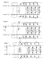
Figure 1 that a first coil SC1 is connected to a second coil SC2 and to a pair of Gate Turn Off Thyristor (GTO) switches GTO1 and GT02 by means of a first point of common coupling PCC1. The cathode of switch GTO1 is connected to a first dc terminal by means of a first main dc line DC1 and the anode of switch GT02 is connected to a second dc terminal by means of a second main dc line DC2. The second coil SC2 is connected to a third coil SC3 and to a pair of GTO switches GT03 and GT04 by means of a second point of common coupling PCC2. The cathode of switch GT03 is connected to the first dc terminal by means of the first main dc line DC1 and the anode of switch GT02 is connected to the second dc terminal by means of the second main dc line DC2. The remaining coils are connected to the first and second main dc lines DC 1 and DC2 in a corresponding manner. - Each pair of GTO switches represents an individual switching stage of an electronic commutator circuit.
- The first and second dc terminals are connected to a suitable dc supply (not shown) such as a thyristor bridge, matrix converter, battery or dc generator. In some cases a dc link inductor LDC will be required as shown in
Figures 2 to 8 as the converter will normally run in a constant current mode. - In
Figure 2 the series connected coils of the stator winding have been omitted to improve clarity but it will be readily appreciated that they extend between the points of common coupling. In other words, the second coil SC2 will extend between the first point of common coupling PCC1 associated with switches GTO1 and GT02 and the second point of common coupling PCC2 associated with switches GT03 and GTO4. - During operation of the electrical machine, dc current flows into the stator winding at a first point in the circular array and flows out of the stator winding at a second point in the circular array. The second point is displaced approximately 180 electrical degrees from the first point. The winding current therefore diverges into two approximately equal paths at the first point and recombines at the second point. In order to effect commutation, the location of the first point or the second point must be indexed one step along the array. The GTO switches are commutated entirely by gate control as described in more detail in British Patent Application
2433360 - A voltage clamping and energy recovery circuit provides three additional functions, namely (i) an alternative path for any current flowing in the outgoing GTO switch when it is turned off (i.e. a conventional switching aid network (snubber) action); (ii) a voltage clamping action on the voltage that may be created when the outgoing GTO switch is turned off; and (iii) an efficient means of storing the energy that would normally be dissipated in a conventional snubber, making it possible to return that energy to some other part of the electrical system. As shown in
Figures 1 and2 , each point of common coupling is connected to a pair of diodes. The first point of common coupling PCC1 is connected to a pair of diodes D1 and D2. The cathode of diode D 1 is connected to a first auxiliary dc line DC3 and the anode of diode D2 is connected to a second auxiliary dc line DC4. The second point of common coupling PCC2 is connected to a pair of diodes D3 and D4. The cathode of diode D3 is connected to the first auxiliary dc line DC3 and the anode of diode D4 is connected to the second auxiliary dc line DC4. The remaining points of common coupling are connected to the first and second auxiliary dc lines DC3 and DC4 in a corresponding manner. - Each pair of diodes represents an individual clamping stage of the voltage clamping and energy recovery circuit and ideally replaces the conventional switching aid network (snubber) components associated with GTO devices. However, practical considerations of allowing for parasitic inductance in the voltage clamping circuit mean that a small snubber (not shown) may still be required for each of the GTO devices. This small snubber will have smaller losses than the conventional snubber without the voltage clamping and energy recovery circuit. For the general case where the stator winding of the electrical machine has n series connected coils with n points of common coupling, it will be readily appreciated that the electronic commutator circuit has n switching stages and the energy recovery circuit has n clamping stages.
- The voltage clamping and energy recovery circuit also includes a first capacitor C 1 connected between the first main dc line DC 1 and the first auxiliary dc line DC3 and a second capacitor C2 connected between the second main dc line DC2 and the second auxiliary dc line DC4. The voltage between the first and second auxiliary dc lines DC3 and DC4 will always be greater than, or equal to, the dc voltage between the first and second main dc lines DC1 and DC2 and is symmetrical about that dc voltage for normal firing patterns. It is therefore possible to feed the energy that is recovered and stored in the first and second capacitors C1 and C2 back to the main dc supply or some other part of the electrical system. In a conventional electrical commutator circuit, this energy would have been dissipated in the switching aid network (snubber).
-
Figure 2 shows one possible arrangement for a dc to dc converter for discharging the first and second capacitors C 1 and C2 that can be used when the electrical machine is designed to operate in a motoring mode only. The dc to dc converter forms part of the energy recovery circuit and provides a means of discharging the first and second capacitors C1 and C2 to the second and first main dc lines DC2 and DC1, respectively. More particularly, the dc to dc converter ofFigure 2 includes a first GTO switch GT05 and a first inductor L1 connected in series between the first auxiliary dc line DC3 and the second main dc line DC2. The anode of the switch GT05 is connected to the first auxiliary dc line DC3 and the cathode is connected to the first inductor L1. The dc to dc converter also includes a second GTO switch GT06 and a second inductor L2 connected in series between the second auxiliary dc line DC4 and the first main dc line DC1. The cathode of the switch GT06 is connected to the second auxiliary dc line DC4 and the anode is connected to the second inductor L2. Finally, the dc to dc converter includes a diode SCR1 having its cathode connected to the junction between the first switch GT05 and the first inductor L1 and its anode connected to the junction between the second switch GT06 and the second inductor L2. Although not shown, a further capacitor can also be connected between the first and second auxiliary dc lines DC3 and DC4. This is a preferred arrangement in the case where the first and second capacitors C 1 and C2 are distributed or multiple capacitors, but it will be readily appreciated that the dc to dc converter is common to all capacitors. Such an arrangement assists with reducing the effect of parasitic inductances within the voltage clamping circuit. - Basic operation of the overall circuit can be understood with reference to
Figure 1 . In normal operation in a motoring mode, current will flow from the second dc terminal along the second main dc line DC2 and into the stator winding at a first point through the associated GTO switch that is turned on by gate control. The winding current diverges into two approximately equal paths at the first point and recombines at a second point that is approximately 180 electrical degrees from the first point. The current flows out of the stator winding at the second point through the associated GTO switch that is also turned on and along the first main dc line DC1 to the first dc terminal. For example, current may flow into the stator winding at the fifth point of common coupling PCC5 through the associated GTO switch and out of the stator winding at the first point of common coupling PCC1 through switch GTO1 with part of the current flowing anti-clockwise as shown inFigure 1 through coils SC6, SC7, SC8 and SC1 and the other part of the current flowing clockwise through coils SC5, SC4, SC3 and SC2. - The vector sum of the individual coil EMFs will charge the first capacitor C1 to a peak dc voltage Vp and the second capacitor C2 to a negative dc peak voltage -Vp. Each GTO device is operated under phase control, by which it is turned on with a gate signal some time after the voltage across it changes polarity due to the machine EMF from negative to positive. This time period is usually expressed as an angle relative to the electrical period and is commonly referred to as the firing angle.
- When the electrical machine is operating in a motoring mode, the voltage in the first main dc line DC1 will be negative with respect to the second main dc line DC2. When the electrical machine is operating in a generating mode, the voltage in the first main dc line DC1 will be positive with respect to the second main dc line DC2. If V1 represents the voltage in the first main dc line DC1, V2 represents the voltage in the second main dc line DC2, V3 represents the voltage in the first auxiliary dc line DC3 and V4 represents the voltage in the second auxiliary dc line DC4 then the ratio k can be defined as: k = (V1-V2) / (V3-V4) the ratio k is dependent on the firing angle and lies between -1 (motoring) and +1 (generating), while no energy is being transferred into the voltage clamping circuit from switching events. The action of the voltage clamping circuit influences the actual working value of Vp, which is greater than the value set by k alone. For the purposes of the following discussion, it will be assumed that since the energy recovery circuit is symmetrical, the peak voltage Vp and all other voltages are considered with respect to the mid point of the circuit.
- Operation of the voltage clamping and energy recovery circuit of
Figure 2 will now be described with reference toFigures 3A to 3C . - If the indexing is such that current is to commutate from the switch GTO1 (i.e. the outgoing switch) to switch GT03 (i.e. the incoming switch) such that the current will change from leaving the stator winding at the first point of common coupling PCC 1 to leaving the stator winding at the second point of common coupling PCC2 (with appropriate similar indexing taking place for the current flow into the stator winding) then the EMF of the electrical machine must cause a forward voltage to be present across the incoming switch GTO3. The current flow at the start of a commutation process (i.e. before the incoming switch GT03 is turned on by gate control) is illustrated in
Figure 3A by the dark grey arrows. - When the incoming switch GT03 turns on, the forward voltage is of the correct polarity and tends to reverse the current in the second coil SC2 (
Figure 1 ) between the first point of common coupling PCC1 and the second point of common coupling PCC2. This will increase the current flowing in the incoming switch GT03 and reduce the current flowing in the outgoing switch GTO1. The current flowing immediately after the incoming switch GT03 is turned on by gate control is illustrated inFigure 3A by the light grey arrows. At some point during the commutation process, the outgoing switch GTO1 will be turned off by gate control. The current that was flowing from the first point of common coupling PCC1 through the outgoing switch GTO1 will now flow through the diode D1 and into the first capacitor C1 which is at the peak voltage Vp. The size of the first capacitor C1 is sufficiently large that the current does not substantially change the peak voltage Vp. The peak current in the diode D 1 is the peak current to be turned off in the outgoing switch GTO1 and under fault conditions this can be the full dc link current. The flow of diode current from the first point of common coupling PCC1 to the first capacitor C1 is illustrated inFigure 3B by the dark grey arrows. The second point of common coupling PCC2 is connected to the first main dc line DC1 through the incoming switch GT03 which is at k*Vp. This means that the voltage across the outgoing switch GTO1 is now (k-1)*Vp forcing the current reversal in the second coil SC2 to complete as indicated by the dark grey arrow ofFigure 3B which shows current flowing from the first point of common coupling PCC1 to the second point of common coupling PCC2. This causes the diode current to fall to zero and turn off. Thus, it will be readily appreciated that the near constant voltage of the first capacitor C1 assists with the overall commutation process and limits the voltage stress experienced by the outgoing switch GTO1. The light grey arrows ofFigure 3B illustrate the flow of current through the incoming switch GT03 once the outgoing switch GTO1 is turned off. This overall commutation action will incrementally pump up the peak voltage Vp at each indexing event. - The above description is directed solely to the indexing of the dc current flowing out of the stator winding. However, it will be readily appreciated that corresponding indexing must also take place for the dc current flowing into the stator winding. The indexing of the dc current flowing into the stator winding may take place at the same time as the indexing of the dc current flowing out of the stator winding or at a different time depending on the particular configuration. For the example given above, where the indexing is such that current will change from leaving the stator winding at the first point of common coupling PCC1 to leaving the stator winding at the second point of common coupling PCC2, then corresponding indexing will be such that current will change from entering the stator winding at the fifth point of common coupling PCC5 to entering the stator winding at the sixth point of common coupling PCC6. Thus the GTO switch associated with the fifth point of common coupling PCC5 will be the outgoing switch and the GTO switch associated with the sixth point of common coupling PCC6 will be the incoming switch. However, for the purposes of the following description, it is more convenient to consider a completely separate indexing event where the switch GT02 is the outgoing switch and the switch GT04 is the incoming switch.
- The indexing is similar to that described above but of the opposite polarity. At the start of the commutation process the incoming switch GT04 is forward biased and can be turned on by gate control. The forward bias voltage tends to reverse the current in the second coil SC2 (
Figure 1 ) between the first point of common coupling PCC1 and the second point of common coupling PCC2. At some point during the commutation process, the outgoing switch GT02 will be turned off by gate control. Any shortage of current at the first point of common coupling PCC 1 will flow through the diode D2 from the second capacitor C2 which is at the negative peak voltage -Vp. The second point of common coupling PCC2 is connected to the second main dc line DC2 through the incoming switch GT04 which is at -k*Vp. This means that the voltage across the outgoing switch GT02 is now (k-1)*Vp forcing the current reversal in coil SC2 to complete. - To avoid the peak voltage Vp becoming too large, the first and second capacitors C 1 and C2 are periodically and simultaneously discharged. This is achieved by turning on the first and second switches GT05 and GT06 of the dc to dc converter by gate control such that current builds up in the first and second inductors L1 and L2 which each have a voltage across them that is equal to (1-k)*Vp (neglecting the effects of indexing events pumping up this voltage and the periodic discharge of the first and second capacitors C1 and C2). When the peak voltage Vp has dropped sufficiently, the first and second switches GT05 and GT06 are turned off by gate control. This causes the voltage across both inductors L1 and L2 to reverse so that the diode SCR2 becomes forward biased and turns on. The current in the series-connected circuit of the first inductor L1, the diode SCR1 and the second inductor L2 decays and when it reaches zero the diode SCR1 turns off thereby restoring the circuit to the original state.
- Monitoring of the voltage on the first and second capacitors C1 and C2 can provide useful information about the operating characteristics and state of the electrical machine. Such information might include the EMF that is being generated in the stator winding and confirmation that the GTO switches of the individual switching stages are conducting current properly. The information could be used to assist in the control of the electrical machine and/or the overall system of which the electrical machine is a part.
- The period between discharges of the first and second capacitors C1 and C2 is not critical to the operation of the circuit and may be a multiple or sub-multiple of the switching frequency for the main GTO devices, for example. The period between discharges does, however, affect the required size of the first and second capacitors C1 and C2 because of the requirement that the voltage on the capacitors should not change substantially. For example, a 10% duty cycle for the first and second switches GT05 and GT06 at full load allows the values of the first and second inductors L1 and L2 to be selected. The preferred duty cycle allows the current in the first and second inductors L1 and L2 to reach zero within the switching period, to reduce the demands on the diode SCR1. Higher duty cycles within the preferred range will reduce the peak current requirement for the first and second switches GT05 and GT06 but will reduce the time available for the reverse recovery of diode SCR1.
- It will be readily appreciated that the dc to dc converter of
Figure 2 is to be used when the electrical machine is designed to operate in a motoring mode only.Figure 4 therefore shows an alternative arrangement for a dc to dc converter that can be used to discharge the first and second capacitors C1 and C2 when the electrical machine is designed to operate normally in a motoring mode, but may occasionally be required to operate in a generating mode. In this case, the diode SCR1 has been replaced by a thyristor (which is also labelled SCR1) and a series connected thyristor SCR3 and resistor DBR are connected between the first and second dc terminals to provide for motor breaking if the supply converter is unable to regenerate into the supply network. This is common practice with marine propulsion drives where the resistor is known as a dynamic breaking resistor (DBR) and the electrical machine operates for most of the time as a motor rather than a generator. When the electrical machine changes from a motoring mode to a generating mode, the polarity of the first and second main dc lines DC1 and DC2 is reversed. Before this reversal takes place, the gate control signal applied to the thyristor SCR1 and the first and second switches GT05 and GT06 must be removed, and the current in the first and second inductors L1 and L2 must be allowed to fall to zero, so that the thyristor SCR1 can recover and block forward voltage. In this state, it is no longer possible to discharge the first and second capacitors C1 and C2 so the main GTO devices should be run as naturally commutated thyristors, maintaining the gate drive to each of the main GTO devices that is turned on until the anode current has reached zero. The firing angle of the main GTO devices is also advanced when the electrical machine changes from a motoring mode to a generating mode. -
Figure 5 shows one possible arrangement for a dc to dc converter that can be used when the electrical machine is designed to operate normally in a generating mode. It will be readily appreciated that the voltage clamping and energy recovery circuit is less important for generating applications since the turn off control of the outgoing GTO switch can be delayed until the current in that GTO switch has fallen to zero with only a minimal effect on performance. In this case, there is no excess current to pump up the first and second capacitors C 1 and C2. - If the outgoing GTO switch is turned off by gate control while still carrying current, the first and second capacitors C1 and C2 will be pumped up as described above. The reversal of voltage polarity between the first and second main dc lines DC 1 and DC2 must be allowed for and so the first and second capacitors C1 and C2 must be discharged to the main dc line that is opposite to that used for the motoring mode. However, the overall operation of the dc to dc converter of
Figure 5 is functionally equivalent to that described above with reference toFigures 3A to 3C . -
Figure 6 shows an arrangement based onFigure 5 where a third capacitor C3 is connected between the first and second auxiliary dc lines DC3 and DC4. Additional capacitors C4 and C5 are also connected between the first auxiliary dc line DC3 and the first main dc line DC1 and between the second auxiliary dc line DC4 and the second main dc line DC2, respectively. The voltage clamping and energy recovery circuit ofFigure 6 therefore includes distributed or multiple capacitors. However, it will be readily appreciated that all of the capacitors C1 to C5 are shared by a single dc to dc converter, which in the arrangement ofFigure 6 is the same as the dc to dc converter ofFigure 5 . The arrangement still has relatively few electrical components, which means lower hardware costs and improved reliability. It will be readily appreciated that this particular arrangement of capacitors can be applied to any of the other voltage clamping and energy recovery circuits described herein. -
Figure 7 shows one possible arrangement for a dc to dc converter that can be used when the electrical machine is designed to operate in both motoring and generating modes. The dc to dc converter is effectively a combination of those shown inFigures 2 and 5 for the motoring and generating modes, respectively. However, the diodes SCR1 and SCR2 are replaced by thyristors (which are also labelled SCR1 and SCR2) that can be turned on and off by gate control for the motoring or generating mode as appropriate. -
Figure 8 shows an alternative resonant dc to dc converter that can be used when the electrical machine is designed to operate normally in a motoring mode. The electrical machine can operate as a generator when the main GTO devices are run as naturally commutated thyristors, maintaining the gate drive to each of the main GTO devices that is turned on until the anode current has reached zero. It will be readily appreciated that such a circuit would need to dissipate energy in the DBR shown inFigure 8 in order to provide a braking effort. The use of a resonant dc to dc converter allows the control of the energy recovery circuit to be further simplified. The first switch GT05 is replaced by a thyristor SCR4 that is turned off automatically when the parallel connected capacitor C6 causes thyristor SCR4 to become reverse biased. Similarly, the second switch GT06 is replaced by a thyristor SCR5 that is turned off automatically when the parallel connected capacitor C7 causes thyristor SCR5 to become reverse biased. Inductors L3 and L4 are connected in series with thyristors SCR4 and SCR5 (and in parallel with the capacitors C6 and C7), respectively, and have small inductances compared to the first and second inductors L1 and L2. A thyristor SCR6 is connected between the junction of the thyristor SCR4 and the first inductor L1 and the junction of the thyristor SCR5 and the second inductor L2. If the electrical machine is only going to be used in a motoring mode then the thyristor SCR6 could be replaced by a simple diode. It is assumed that thyristor SCR6 will be gated on whenever the electrical machine is operating in a motoring mode so it will behave like a diode in the following description. - When thyristor SCR4 is turned on by gate control to discharge the first capacitor C1 of the voltage clamping circuit, the current flowing through it is, by principle of superposition, the current that would flow in the previous (non resonant) dc to dc converter for motoring applications plus the sinusoidal resonant current due to the capacitor C6 and the inductor L3 being shorted with an initial charge on the capacitor C6. The first of these currents will also be slightly modified by the fact that the relevant inductance is the sum of the inductances of the two inductors L1 and L3 but this is dominated by the larger inductance of the first inductor L1. With the correct choice of component values, the sinusoidal current through the capacitor C6 will be sufficiently large to cause the total current through the thyristor SCR4 to attempt to go negative, which will automatically cause the thyristor SCR4 to turn off. The current that has been established in the first inductor L1 (and in a similar way in the second inductor L2 when the thyristor SCR5 is turned on by gate control to discharge the second capacitor C2 of the voltage clamping circuit) will continue to flow and is supplied by the charging of the capacitors C6 and C7 until a time when the thyristor SCR6 becomes forward biased and commutates the capacitors C6 and C7.
- The use of a resonant dc to dc converter means that the first and second capacitors C 1 and C2 can be selectively discharged by turning on the thyristors SCR4 and SCR5 by gate control when the voltage on the capacitors C1 and C2 exceeds a particular threshold. Thereafter, the thyristors SCR4 and SCR5 will recover naturally by the well-known resonant commutation process.
- A similar resonant dc to dc converter can be used in the generating mode with the appropriate reversal of the connections between the first and second inductors L1 and L2 and the first and second main dc lines D1 and DC2. However, the selection of suitable component values to cause correct operation in the generating mode is more difficult. These difficulties would increase for circuits designed to work in both motoring and generating modes but alternative dc to dc converter designs may offer workable alternatives.
-
Figure 9 shows separate dc to dc converters for the first and second auxiliary dc lines DC3 and DC4. Separate dc to dc converters may be needed if practical component values result in the first and second auxiliary dc lines DC3 and DC4 not tracking each other. The first dc to dc converter ofFigure 9 includes a first GTO switch GT05 and a first inductor L1 connected in series between the first auxiliary dc line DC3 and the second main dc line DC2, and a thyristor SCR6 having its cathode connected to the junction between the first switch GT05 and the first inductor L1 and its anode connected to the second main dc line DC2. The second dc to dc converter ofFigure 9 includes a second GTO switch GT06 and a second inductor L2 connected in series between the second auxiliary dc line DC4 and the first main dc line DC1, and a thyristor SCR7 having its anode connected to the junction between the second switch GT06 and the second inductor L2 and its cathode connected to the first main dc line DC1. The thyristors SCR6 and SCR7 are always on when the electrical machine is operating in a motoring mode, but must be turned off when the electrical machine is operating in a generating mode. If the electrical machine is to operate only in a motoring mode then thyristors SCR6 and SCR7 can be replaced by diodes. In an embodiment of the circuit ofFigure 9 when only being used for motoring then two identical control circuits would be used, one for the first switch GT05 and another for the second switch GT06. Control inputs to the control circuit would be the current in the relevant inductor (i.e. the first inductor L1 for the first switch GT05 and the second inductor L2 for the second switch GT06), sensed by a current transformer, and the forward voltage across the GTO switch that is being controlled. The control circuit would turn the GTO switch on when the forward voltage exceeds a threshold and turn it off when the current in the relevant inductor reaches a second threshold. The control circuit may be designed so that no auxiliary power and no other control inputs are needed. - In the more general case, control of thyristors SCR6 and SCR7, and the selection of the trigger voltage across the GTO switch may be required. The selection of the trigger voltage provides a means of controlling the clamp voltage, which may have benefits in certain applications. Such functions would require further input controls to the control circuit.
Claims (15)
- A circuit for use with a stator winding of an electrical machine, the stator winding including a number of coils (SC1-SC6) linked by the same number of points of common coupling (PCC1-PCC6), the circuit comprising:an electronic commutator circuit having the same number of switching stages, each switching stage being connected between a respective one of the points of common coupling (PCC1-PCC6) and first and second main dc lines (DC1, DC2) and including:a first reverse blocking semiconductor power device (GTO1, GT03) capable of being turned on and off by gate control having its cathode connected to the first main dc line (DC1); anda second reverse blocking semiconductor power device (GTO2, GT04) capable of being turned on and off by gate control having itsanode connected to the second main dc line (DC2); a voltage clamping circuit including:the same number of clamping stages, each clamping stage being connected between a respective one of the points of common coupling (PCC1-PCC6) and first and second auxiliary dc lines (DC3, DC4) andincluding a first diode (D1, D3) having its cathode connected to the first auxiliary dc line (DC3), and a second diode (D2, D4) having its anode connected to the second auxiliary dc line (DC4);a first capacitor (C1) connected between the first main dc line (DC1) and the first auxiliary dc line (DC3); anda second capacitor (C2) connected between the second main dc line(DC2) and the second auxiliary dc line (DC4); and means for selectively discharging the first and second capacitors (C1, C2).
- A circuit according to claim 1, wherein the means for selectively discharging the first and second capacitors (C1, C2) is an energy recovery circuit for recovering the energy stored in the first and second capacitors.
- A circuit according to claim 2, wherein the energy recovery circuit includes a dc to dc converter (GTO5, L1, GT06, L2, SCR1; Figure 2) means for selectively discharging the first capacitor (C1) to one of the first and second main dc lines (DC1, DC2) and selectively discharging the second capacitor (C2) to the other of the first and second main dc lines (DC1, DC2).
- A circuit according to claim 2, wherein the energy recovery circuit includes a first dc to dc converter means (GTO5, L1, SCR6; Figure 9) for selectively discharging the first capacitor (C1) to one of the first and second main dc lines (DC1, DC2) and a second dc to dc converter means (GTO6, L2, SCR7; Figure 9) for selectively discharging the second capacitor (C2) to the other of the first and second main dc lines (DC1, DC2).
- A circuit according to any preceding claim, wherein the voltage clamping circuit further includes a third capacitor (C3; Figure 6) connected between the first and second auxiliary dc lines (DC3, DC4).
- A circuit according to any preceding claim, wherein the voltage clamping circuit further comprises a plurality of first capacitors connected between the first main dc line and the first auxiliary dc line and a plurality of second capacitors connected between the second main dc line and the second auxiliary dc line.
- A circuit according to any preceding claim, further comprising first and second dc terminals and wherein a series connected thyristor and resistor (SR3, DBR; Figure 4) are connected between the first and second dc terminals.
- A method of recovering energy from an electronic commutator circuit for use with a stator winding of an electrical machine, the stator winding having a number of coils (SC1-SC6) linked by the same number of points of common coupling (PCC1-PCC6), the electronic commutator circuit having the same number of switching stages, each switching stage being connected between a respective one of the points of common coupling (PCC1-PCC6) and first and second main dc lines (DC1, DC2) and including:a first reverse blocking semiconductor power device (GTO1, GT03) capable of being turned on and off by gate control having its cathode connected to the first main dc line (DC1); anda second reverse blocking semiconductor power device (GTO2, GT04) capable of being turned on and off by gate control having itsanode connected to the second main dc line (DC2); the method comprising the steps of:when one of the first or second reverse blocking semiconductor power devices (GTO1) of a switching stage is turned off by gate control, using the current flowing through said one of the first or second reverse blocking semiconductor power devices (GTO1) to charge a capacitor (C1); andselectively discharging the capacitor (C1).
- A method according to claim 8, wherein the capacitor (C1) is selectively discharged by an energy recovery circuit for recovering the energy stored in the capacitor.
- A method according to claim 8 or claim 9, wherein the capacitor (C1) is selectively discharged by a dc to dc converter means.
- A method according to claim 10, wherein the dc to dc converter means is a resonant dc to dc converter means.
- A method according to any of claims 8 to 11, wherein the capacitor (C1) is selectively discharged to one of the first and second main dc lines (DC1, DC2).
- A method according to any of claims 8 to 12, further comprising the step of monitoring the voltage on the capacitor (C1) to determine information about the operating characteristics of the electrical machine.
- An electrical machine comprising a moving part, a stator, a stator winding having a number of coils linked by the same number of points of common coupling and a circuit according to any of claims 1 to 7, wherein each switching stage of the electronic commutator circuit is connected between a respective one of the points of common coupling and first and second main dc lines and each clamping stage of the voltage clamping circuit is connected between a respective one of the points of common coupling and the first and second auxiliary dc lines.
- A method of controlling an electrical machine according to claim 14, wherein the voltage between the first and second auxiliary dc lines is substantially constant for all operating conditions of the electrical machine or varies according to the operating condition of the electrical machine.
Applications Claiming Priority (1)
| Application Number | Priority Date | Filing Date | Title |
|---|---|---|---|
| GB0723548.4A GB2455144B (en) | 2007-12-01 | 2007-12-01 | Voltage clamping and energy recovery circuits |
Publications (3)
| Publication Number | Publication Date |
|---|---|
| EP2066019A2 true EP2066019A2 (en) | 2009-06-03 |
| EP2066019A3 EP2066019A3 (en) | 2015-03-25 |
| EP2066019B1 EP2066019B1 (en) | 2018-03-07 |
Family
ID=38962462
Family Applications (1)
| Application Number | Title | Priority Date | Filing Date |
|---|---|---|---|
| EP08020685.7A Not-in-force EP2066019B1 (en) | 2007-12-01 | 2008-11-28 | Voltage clamping and energy recovery circuits |
Country Status (7)
| Country | Link |
|---|---|
| US (1) | US8040094B2 (en) |
| EP (1) | EP2066019B1 (en) |
| JP (1) | JP5452907B2 (en) |
| KR (1) | KR101485187B1 (en) |
| CN (1) | CN101447753B (en) |
| AU (1) | AU2008251997B2 (en) |
| GB (1) | GB2455144B (en) |
Families Citing this family (5)
| Publication number | Priority date | Publication date | Assignee | Title |
|---|---|---|---|---|
| US8619445B1 (en) | 2013-03-15 | 2013-12-31 | Arctic Sand Technologies, Inc. | Protection of switched capacitor power converter |
| GB2592543B (en) | 2014-03-14 | 2022-01-26 | Arctic Sand Technologies Inc | Charge pump stability control |
| US10693368B2 (en) | 2014-03-14 | 2020-06-23 | Psemi Corporation | Charge pump stability control |
| CN108028600B (en) | 2015-07-08 | 2022-03-08 | 派更半导体公司 | Switched capacitor power converter |
| MX2020003028A (en) | 2017-09-20 | 2020-11-06 | Mainspring Energy Inc | Auto-braking for an electromagnetic machine. |
Citations (1)
| Publication number | Priority date | Publication date | Assignee | Title |
|---|---|---|---|---|
| GB2433360A (en) | 2005-12-17 | 2007-06-20 | Alstom Power Conversion Ltd | Electric commutator motors |
Family Cites Families (5)
| Publication number | Priority date | Publication date | Assignee | Title |
|---|---|---|---|---|
| JP2842496B2 (en) * | 1992-10-19 | 1999-01-06 | 三菱電機株式会社 | Chopper device |
| JPH08223931A (en) * | 1995-02-17 | 1996-08-30 | Toshiba Corp | Power conversion apparatus |
| DE60042601D1 (en) * | 1999-08-12 | 2009-09-03 | Yaskawa Denki Kitakyushu Kk | METHOD FOR REGULATING THE ZERO POINT POTENTIAL OF A TRACKER WITH ZERO-POINT LIMITATION |
| CN100384074C (en) * | 2002-06-28 | 2008-04-23 | 河南电力试验研究所 | Five-level high-voltage frequency converter |
| US7342811B2 (en) * | 2005-05-27 | 2008-03-11 | Cherokee International Corporation | Lossless clamp circuit for DC-DC converters |
-
2007
- 2007-12-01 GB GB0723548.4A patent/GB2455144B/en not_active Expired - Fee Related
-
2008
- 2008-11-28 EP EP08020685.7A patent/EP2066019B1/en not_active Not-in-force
- 2008-11-28 JP JP2008304223A patent/JP5452907B2/en not_active Expired - Fee Related
- 2008-12-01 AU AU2008251997A patent/AU2008251997B2/en not_active Ceased
- 2008-12-01 CN CN2008101792407A patent/CN101447753B/en not_active Expired - Fee Related
- 2008-12-01 KR KR20080120739A patent/KR101485187B1/en active IP Right Grant
- 2008-12-01 US US12/315,234 patent/US8040094B2/en not_active Expired - Fee Related
Patent Citations (1)
| Publication number | Priority date | Publication date | Assignee | Title |
|---|---|---|---|---|
| GB2433360A (en) | 2005-12-17 | 2007-06-20 | Alstom Power Conversion Ltd | Electric commutator motors |
Also Published As
| Publication number | Publication date |
|---|---|
| CN101447753A (en) | 2009-06-03 |
| JP5452907B2 (en) | 2014-03-26 |
| EP2066019B1 (en) | 2018-03-07 |
| JP2009178024A (en) | 2009-08-06 |
| KR101485187B1 (en) | 2015-01-22 |
| GB0723548D0 (en) | 2008-01-09 |
| GB2455144B (en) | 2012-08-15 |
| AU2008251997A1 (en) | 2009-06-18 |
| GB2455144A (en) | 2009-06-03 |
| CN101447753B (en) | 2013-02-13 |
| US20090146596A1 (en) | 2009-06-11 |
| EP2066019A3 (en) | 2015-03-25 |
| AU2008251997B2 (en) | 2011-12-15 |
| US8040094B2 (en) | 2011-10-18 |
| KR20090057166A (en) | 2009-06-04 |
Similar Documents
| Publication | Publication Date | Title |
|---|---|---|
| US6495985B1 (en) | Operation of a switched reluctance machine from dual supply voltages | |
| JP5430568B2 (en) | Single-switch controlled reluctance machine | |
| EP2066019B1 (en) | Voltage clamping and energy recovery circuits | |
| US11689072B2 (en) | Demagnetization of the rotor of an externally excited synchronous machine | |
| KR101012781B1 (en) | A circuit for use with switched reluctance machines | |
| US7372232B2 (en) | Apparatus for drive control, power conversion, and start-up control in a PMBDCM or two-phase SRM drive system | |
| US20190275890A1 (en) | Method for Switching off a Current-Excited Synchronous Machine of a Motor Vehicle | |
| US6987375B2 (en) | Dual-stage drive for switched reluctance electric machines | |
| Dahmane et al. | A novel boost capacitor circuit to enhance the performance of the switched reluctance motor | |
| EP3789231A1 (en) | Efficient regenerative electrical braking | |
| KR102299110B1 (en) | Power converting circuit | |
| CN114389236A (en) | Power conversion device | |
| US9379659B2 (en) | Lossless snubber drive for a permanent magnet synchronous motor | |
| Barnes et al. | Selecting power electronic converters for single phase switched reluctance motors | |
| JP4161253B2 (en) | Multiphase AC voltage regulator | |
| US11431272B2 (en) | Energy recovery circuitry | |
| EP4293895A1 (en) | A motor control controller system and methods | |
| Shambhavi et al. | Power Converter Configurations for Switched Reluctance Motors: A | |
| JP3158093B2 (en) | Motor drive circuit | |
| EP4256704A1 (en) | Gate driver | |
| RU2037259C1 (en) | Inverter for feeding reluctance inductor motor | |
| CN112739568A (en) | Control device for inverter, inverter for vehicle, vehicle and method for operating inverter | |
| CS261193B1 (en) | Connection of inverter for alternating-current contactless engines' frequency control |
Legal Events
| Date | Code | Title | Description |
|---|---|---|---|
| PUAI | Public reference made under article 153(3) epc to a published international application that has entered the european phase |
Free format text: ORIGINAL CODE: 0009012 |
|
| AK | Designated contracting states |
Kind code of ref document: A2 Designated state(s): AT BE BG CH CY CZ DE DK EE ES FI FR GB GR HR HU IE IS IT LI LT LU LV MC MT NL NO PL PT RO SE SI SK TR |
|
| AX | Request for extension of the european patent |
Extension state: AL BA MK RS |
|
| RAP1 | Party data changed (applicant data changed or rights of an application transferred) |
Owner name: GE ENERGY POWER CONVERSION TECHNOLOGY LIMITED |
|
| PUAL | Search report despatched |
Free format text: ORIGINAL CODE: 0009013 |
|
| AK | Designated contracting states |
Kind code of ref document: A3 Designated state(s): AT BE BG CH CY CZ DE DK EE ES FI FR GB GR HR HU IE IS IT LI LT LU LV MC MT NL NO PL PT RO SE SI SK TR |
|
| AX | Request for extension of the european patent |
Extension state: AL BA MK RS |
|
| RIC1 | Information provided on ipc code assigned before grant |
Ipc: H02P 25/02 20060101AFI20150219BHEP |
|
| 17P | Request for examination filed |
Effective date: 20150813 |
|
| RBV | Designated contracting states (corrected) |
Designated state(s): AT BE BG CH CY CZ DE DK EE ES FI FR GB GR HR HU IE IS IT LI LT LU LV MC MT NL NO PL PT RO SE SI SK TR |
|
| AKX | Designation fees paid |
Designated state(s): AT BE BG CH CY CZ DE DK EE ES FI FR GB GR HR HU IE IS IT LI LT LU LV MC MT NL NO PL PT RO SE SI SK TR |
|
| AXX | Extension fees paid |
Extension state: RS Extension state: AL Extension state: MK Extension state: BA |
|
| GRAP | Despatch of communication of intention to grant a patent |
Free format text: ORIGINAL CODE: EPIDOSNIGR1 |
|
| INTG | Intention to grant announced |
Effective date: 20171017 |
|
| GRAS | Grant fee paid |
Free format text: ORIGINAL CODE: EPIDOSNIGR3 |
|
| GRAA | (expected) grant |
Free format text: ORIGINAL CODE: 0009210 |
|
| AK | Designated contracting states |
Kind code of ref document: B1 Designated state(s): AT BE BG CH CY CZ DE DK EE ES FI FR GB GR HR HU IE IS IT LI LT LU LV MC MT NL NO PL PT RO SE SI SK TR |
|
| REG | Reference to a national code |
Ref country code: GB Ref legal event code: FG4D |
|
| REG | Reference to a national code |
Ref country code: CH Ref legal event code: EP Ref country code: AT Ref legal event code: REF Ref document number: 977570 Country of ref document: AT Kind code of ref document: T Effective date: 20180315 |
|
| REG | Reference to a national code |
Ref country code: IE Ref legal event code: FG4D |
|
| REG | Reference to a national code |
Ref country code: DE Ref legal event code: R096 Ref document number: 602008054292 Country of ref document: DE |
|
| REG | Reference to a national code |
Ref country code: NL Ref legal event code: MP Effective date: 20180307 |
|
| REG | Reference to a national code |
Ref country code: LT Ref legal event code: MG4D |
|
| PG25 | Lapsed in a contracting state [announced via postgrant information from national office to epo] |
Ref country code: CY Free format text: LAPSE BECAUSE OF FAILURE TO SUBMIT A TRANSLATION OF THE DESCRIPTION OR TO PAY THE FEE WITHIN THE PRESCRIBED TIME-LIMIT Effective date: 20180307 Ref country code: HR Free format text: LAPSE BECAUSE OF FAILURE TO SUBMIT A TRANSLATION OF THE DESCRIPTION OR TO PAY THE FEE WITHIN THE PRESCRIBED TIME-LIMIT Effective date: 20180307 Ref country code: FI Free format text: LAPSE BECAUSE OF FAILURE TO SUBMIT A TRANSLATION OF THE DESCRIPTION OR TO PAY THE FEE WITHIN THE PRESCRIBED TIME-LIMIT Effective date: 20180307 Ref country code: NO Free format text: LAPSE BECAUSE OF FAILURE TO SUBMIT A TRANSLATION OF THE DESCRIPTION OR TO PAY THE FEE WITHIN THE PRESCRIBED TIME-LIMIT Effective date: 20180607 Ref country code: ES Free format text: LAPSE BECAUSE OF FAILURE TO SUBMIT A TRANSLATION OF THE DESCRIPTION OR TO PAY THE FEE WITHIN THE PRESCRIBED TIME-LIMIT Effective date: 20180307 Ref country code: LT Free format text: LAPSE BECAUSE OF FAILURE TO SUBMIT A TRANSLATION OF THE DESCRIPTION OR TO PAY THE FEE WITHIN THE PRESCRIBED TIME-LIMIT Effective date: 20180307 |
|
| REG | Reference to a national code |
Ref country code: AT Ref legal event code: MK05 Ref document number: 977570 Country of ref document: AT Kind code of ref document: T Effective date: 20180307 |
|
| PG25 | Lapsed in a contracting state [announced via postgrant information from national office to epo] |
Ref country code: SE Free format text: LAPSE BECAUSE OF FAILURE TO SUBMIT A TRANSLATION OF THE DESCRIPTION OR TO PAY THE FEE WITHIN THE PRESCRIBED TIME-LIMIT Effective date: 20180307 Ref country code: LV Free format text: LAPSE BECAUSE OF FAILURE TO SUBMIT A TRANSLATION OF THE DESCRIPTION OR TO PAY THE FEE WITHIN THE PRESCRIBED TIME-LIMIT Effective date: 20180307 Ref country code: BG Free format text: LAPSE BECAUSE OF FAILURE TO SUBMIT A TRANSLATION OF THE DESCRIPTION OR TO PAY THE FEE WITHIN THE PRESCRIBED TIME-LIMIT Effective date: 20180607 Ref country code: GR Free format text: LAPSE BECAUSE OF FAILURE TO SUBMIT A TRANSLATION OF THE DESCRIPTION OR TO PAY THE FEE WITHIN THE PRESCRIBED TIME-LIMIT Effective date: 20180608 |
|
| REG | Reference to a national code |
Ref country code: FR Ref legal event code: PLFP Year of fee payment: 11 |
|
| PG25 | Lapsed in a contracting state [announced via postgrant information from national office to epo] |
Ref country code: RO Free format text: LAPSE BECAUSE OF FAILURE TO SUBMIT A TRANSLATION OF THE DESCRIPTION OR TO PAY THE FEE WITHIN THE PRESCRIBED TIME-LIMIT Effective date: 20180307 Ref country code: IT Free format text: LAPSE BECAUSE OF FAILURE TO SUBMIT A TRANSLATION OF THE DESCRIPTION OR TO PAY THE FEE WITHIN THE PRESCRIBED TIME-LIMIT Effective date: 20180307 Ref country code: EE Free format text: LAPSE BECAUSE OF FAILURE TO SUBMIT A TRANSLATION OF THE DESCRIPTION OR TO PAY THE FEE WITHIN THE PRESCRIBED TIME-LIMIT Effective date: 20180307 Ref country code: PL Free format text: LAPSE BECAUSE OF FAILURE TO SUBMIT A TRANSLATION OF THE DESCRIPTION OR TO PAY THE FEE WITHIN THE PRESCRIBED TIME-LIMIT Effective date: 20180307 Ref country code: NL Free format text: LAPSE BECAUSE OF FAILURE TO SUBMIT A TRANSLATION OF THE DESCRIPTION OR TO PAY THE FEE WITHIN THE PRESCRIBED TIME-LIMIT Effective date: 20180307 |
|
| PG25 | Lapsed in a contracting state [announced via postgrant information from national office to epo] |
Ref country code: SK Free format text: LAPSE BECAUSE OF FAILURE TO SUBMIT A TRANSLATION OF THE DESCRIPTION OR TO PAY THE FEE WITHIN THE PRESCRIBED TIME-LIMIT Effective date: 20180307 Ref country code: CZ Free format text: LAPSE BECAUSE OF FAILURE TO SUBMIT A TRANSLATION OF THE DESCRIPTION OR TO PAY THE FEE WITHIN THE PRESCRIBED TIME-LIMIT Effective date: 20180307 Ref country code: AT Free format text: LAPSE BECAUSE OF FAILURE TO SUBMIT A TRANSLATION OF THE DESCRIPTION OR TO PAY THE FEE WITHIN THE PRESCRIBED TIME-LIMIT Effective date: 20180307 |
|
| REG | Reference to a national code |
Ref country code: DE Ref legal event code: R097 Ref document number: 602008054292 Country of ref document: DE |
|
| PG25 | Lapsed in a contracting state [announced via postgrant information from national office to epo] |
Ref country code: PT Free format text: LAPSE BECAUSE OF FAILURE TO SUBMIT A TRANSLATION OF THE DESCRIPTION OR TO PAY THE FEE WITHIN THE PRESCRIBED TIME-LIMIT Effective date: 20180709 |
|
| PLBE | No opposition filed within time limit |
Free format text: ORIGINAL CODE: 0009261 |
|
| STAA | Information on the status of an ep patent application or granted ep patent |
Free format text: STATUS: NO OPPOSITION FILED WITHIN TIME LIMIT |
|
| PG25 | Lapsed in a contracting state [announced via postgrant information from national office to epo] |
Ref country code: DK Free format text: LAPSE BECAUSE OF FAILURE TO SUBMIT A TRANSLATION OF THE DESCRIPTION OR TO PAY THE FEE WITHIN THE PRESCRIBED TIME-LIMIT Effective date: 20180307 |
|
| 26N | No opposition filed |
Effective date: 20181210 |
|
| PG25 | Lapsed in a contracting state [announced via postgrant information from national office to epo] |
Ref country code: SI Free format text: LAPSE BECAUSE OF FAILURE TO SUBMIT A TRANSLATION OF THE DESCRIPTION OR TO PAY THE FEE WITHIN THE PRESCRIBED TIME-LIMIT Effective date: 20180307 |
|
| REG | Reference to a national code |
Ref country code: CH Ref legal event code: PL |
|
| PG25 | Lapsed in a contracting state [announced via postgrant information from national office to epo] |
Ref country code: MC Free format text: LAPSE BECAUSE OF FAILURE TO SUBMIT A TRANSLATION OF THE DESCRIPTION OR TO PAY THE FEE WITHIN THE PRESCRIBED TIME-LIMIT Effective date: 20180307 Ref country code: LU Free format text: LAPSE BECAUSE OF NON-PAYMENT OF DUE FEES Effective date: 20181128 |
|
| REG | Reference to a national code |
Ref country code: BE Ref legal event code: MM Effective date: 20181130 |
|
| REG | Reference to a national code |
Ref country code: IE Ref legal event code: MM4A |
|
| PG25 | Lapsed in a contracting state [announced via postgrant information from national office to epo] |
Ref country code: CH Free format text: LAPSE BECAUSE OF NON-PAYMENT OF DUE FEES Effective date: 20181130 Ref country code: LI Free format text: LAPSE BECAUSE OF NON-PAYMENT OF DUE FEES Effective date: 20181130 |
|
| PG25 | Lapsed in a contracting state [announced via postgrant information from national office to epo] |
Ref country code: IE Free format text: LAPSE BECAUSE OF NON-PAYMENT OF DUE FEES Effective date: 20181128 |
|
| PG25 | Lapsed in a contracting state [announced via postgrant information from national office to epo] |
Ref country code: BE Free format text: LAPSE BECAUSE OF NON-PAYMENT OF DUE FEES Effective date: 20181130 |
|
| PG25 | Lapsed in a contracting state [announced via postgrant information from national office to epo] |
Ref country code: MT Free format text: LAPSE BECAUSE OF NON-PAYMENT OF DUE FEES Effective date: 20181128 |
|
| PGFP | Annual fee paid to national office [announced via postgrant information from national office to epo] |
Ref country code: DE Payment date: 20191021 Year of fee payment: 12 |
|
| PGFP | Annual fee paid to national office [announced via postgrant information from national office to epo] |
Ref country code: FR Payment date: 20191022 Year of fee payment: 12 |
|
| PG25 | Lapsed in a contracting state [announced via postgrant information from national office to epo] |
Ref country code: TR Free format text: LAPSE BECAUSE OF FAILURE TO SUBMIT A TRANSLATION OF THE DESCRIPTION OR TO PAY THE FEE WITHIN THE PRESCRIBED TIME-LIMIT Effective date: 20180307 |
|
| PGFP | Annual fee paid to national office [announced via postgrant information from national office to epo] |
Ref country code: GB Payment date: 20191022 Year of fee payment: 12 |
|
| PG25 | Lapsed in a contracting state [announced via postgrant information from national office to epo] |
Ref country code: HU Free format text: LAPSE BECAUSE OF FAILURE TO SUBMIT A TRANSLATION OF THE DESCRIPTION OR TO PAY THE FEE WITHIN THE PRESCRIBED TIME-LIMIT; INVALID AB INITIO Effective date: 20081128 |
|
| PG25 | Lapsed in a contracting state [announced via postgrant information from national office to epo] |
Ref country code: IS Free format text: LAPSE BECAUSE OF FAILURE TO SUBMIT A TRANSLATION OF THE DESCRIPTION OR TO PAY THE FEE WITHIN THE PRESCRIBED TIME-LIMIT Effective date: 20180707 |
|
| REG | Reference to a national code |
Ref country code: DE Ref legal event code: R119 Ref document number: 602008054292 Country of ref document: DE |
|
| GBPC | Gb: european patent ceased through non-payment of renewal fee |
Effective date: 20201128 |
|
| PG25 | Lapsed in a contracting state [announced via postgrant information from national office to epo] |
Ref country code: FR Free format text: LAPSE BECAUSE OF NON-PAYMENT OF DUE FEES Effective date: 20201130 |
|
| PG25 | Lapsed in a contracting state [announced via postgrant information from national office to epo] |
Ref country code: DE Free format text: LAPSE BECAUSE OF NON-PAYMENT OF DUE FEES Effective date: 20210601 Ref country code: GB Free format text: LAPSE BECAUSE OF NON-PAYMENT OF DUE FEES Effective date: 20201128 |