EP2063486A1 - Antenna apparatus - Google Patents
Antenna apparatus Download PDFInfo
- Publication number
- EP2063486A1 EP2063486A1 EP08019387A EP08019387A EP2063486A1 EP 2063486 A1 EP2063486 A1 EP 2063486A1 EP 08019387 A EP08019387 A EP 08019387A EP 08019387 A EP08019387 A EP 08019387A EP 2063486 A1 EP2063486 A1 EP 2063486A1
- Authority
- EP
- European Patent Office
- Prior art keywords
- antenna
- matching circuit
- ground
- transmission line
- antenna apparatus
- Prior art date
- Legal status (The legal status is an assumption and is not a legal conclusion. Google has not performed a legal analysis and makes no representation as to the accuracy of the status listed.)
- Withdrawn
Links
- 230000005540 biological transmission Effects 0.000 claims abstract description 23
- 239000004020 conductor Substances 0.000 claims abstract description 16
- 239000000126 substance Substances 0.000 claims abstract description 16
- 239000003990 capacitor Substances 0.000 claims abstract description 15
- 230000005855 radiation Effects 0.000 claims abstract description 15
- 239000000758 substrate Substances 0.000 description 11
- 238000010586 diagram Methods 0.000 description 10
- 230000001413 cellular effect Effects 0.000 description 3
- 238000006243 chemical reaction Methods 0.000 description 3
- 239000011347 resin Substances 0.000 description 3
- 229920005989 resin Polymers 0.000 description 3
- 230000004075 alteration Effects 0.000 description 1
- 230000002542 deteriorative effect Effects 0.000 description 1
- 239000000284 extract Substances 0.000 description 1
- 239000000463 material Substances 0.000 description 1
- 230000007246 mechanism Effects 0.000 description 1
- 238000012986 modification Methods 0.000 description 1
- 230000004048 modification Effects 0.000 description 1
- 230000005404 monopole Effects 0.000 description 1
- 238000004804 winding Methods 0.000 description 1
Images

Classifications
-
- H—ELECTRICITY
- H01—ELECTRIC ELEMENTS
- H01Q—ANTENNAS, i.e. RADIO AERIALS
- H01Q1/00—Details of, or arrangements associated with, antennas
- H01Q1/12—Supports; Mounting means
- H01Q1/22—Supports; Mounting means by structural association with other equipment or articles
- H01Q1/2283—Supports; Mounting means by structural association with other equipment or articles mounted in or on the surface of a semiconductor substrate as a chip-type antenna or integrated with other components into an IC package
-
- H—ELECTRICITY
- H01—ELECTRIC ELEMENTS
- H01Q—ANTENNAS, i.e. RADIO AERIALS
- H01Q1/00—Details of, or arrangements associated with, antennas
- H01Q1/36—Structural form of radiating elements, e.g. cone, spiral, umbrella; Particular materials used therewith
- H01Q1/362—Structural form of radiating elements, e.g. cone, spiral, umbrella; Particular materials used therewith for broadside radiating helical antennas
-
- H—ELECTRICITY
- H01—ELECTRIC ELEMENTS
- H01Q—ANTENNAS, i.e. RADIO AERIALS
- H01Q23/00—Antennas with active circuits or circuit elements integrated within them or attached to them
Definitions
- the present invention relates to an antenna apparatus used in a cellular phone and the like to receive a television signal.
- antenna apparatuses for a television device built in a mobile device have been developed. Since a broadcast band for television broadcast signals is a wide band (for example, 470 MHz to 770 MHz in Japan), a wideband antenna apparatus is needed to correspond to the wide band when one antenna is intended to be used. For example, in an antenna apparatus disclosed in Japanese Unexamined Patent Application Publication No.
- a DC block capacitor is connected to a feeding section of a radiation conductor, a resonant circuit is formed by connecting a variable capacitance diode between one end of the radiation conductor and the DC block capacitor, and a connecting point between the variable capacitance diode and the DC block capacitor is connected to an antenna earth via a high frequency choke coil.
- the antenna apparatus is tuned to a used frequency by superimposing a frequency control voltage of the voltage control oscillator on a voltage of the feeding section.
- Fig. 4 is an exterior diagram illustrating an antenna apparatus having a tunable matching circuit tuning to the used frequency and functioning as a matching circuit.
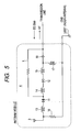
- Fig. 5 is a diagram illustrating a configuration of an antenna module of the antenna apparatus shown in Fig. 4 .
- the antenna apparatus includes an antenna element (helical antenna) 3 formed by winding a radiation conductor 2 in a helical shape around an outer periphery of a base substance 1 made of resin and a tunable matching circuit 4 capable of controlling a used frequency band with a signal from a tuner.
- a ground surface GND for providing a ground potential of the tunable matching circuit 4 is formed just below the antenna element 3.
- the tunable matching circuit 4 includes a resonant circuit formed of varactor diodes 11 and 12 and inductors 13, 14, and 15 as shown in Fig. 5 .
- An anode of one side varactor diode 11 connected to the antenna element 3 is connected via a resistor 16 to a ground GND formed just below the antenna.
- an anode of the other side varactor diode 12 and one end of an inductor 15 is connected to the ground GND formed just below the antenna via an inductor 17.
- one end of a bypass line L for applying a tuning signal Vt is connected to cathodes of the varactor diodes 11 and 12, and the other end of the bypass line L is connected to a transmission line.
- a tuner side end of the inductor 15 is connected to a tuner via a DC cut capacitor 18.
- capacitances of the varactor diodes 11 and 12 are changed by a tuning signal Vt applied from the tuner to the cathodes of the varactor diodes 11 and 12, and an antenna side tuning frequency is controlled.
- a tuning frequency signal is acquired from a wideband high-frequency reception signal output from the antenna element 3, and is transmitted to the tuner.
- the ground GND is formed just below the antenna.
- the ground GND becomes a factor of lowering a gain and a radiation efficiency of the antenna, thereby deteriorating antenna performance.
- the antenna apparatus includes: an antenna element having a radiation conductor formed on a surface of a base substance; and a matching circuit formed on the base substance to match with the radiation conductor and having a variable capacitor to which a control voltage for controlling capacitance is applied from a reception circuit formed outside the base substance.
- a ground potential of the matching circuit is applied via a transmission line for transmitting an RF signal output from the matching circuit to the reception circuit.
- the ground potential of the matching circuit is applied via the transmission line for transmitting the RF signal output from the matching circuit to the reception circuit, it is possible to remove a ground surface for applying a ground potential to the matching circuit of the antenna from just below the antenna. Thus, it is possible to prevent the antenna element from being affected by a ground line.
- an inductor be connected in series between the transmission line and a ground of the reception circuit on the reception circuit side.
- the inductor is connected in series between the transmission line and the ground of the reception circuit, it is possible to provide a DC ground and a high frequency ground on the reception circuit side to the matching circuit.
- the voltage applied to the variable capacitor of the matching circuit be supplied via a line separate from the transmission line.
- the matching circuit have two variable capacitors connected to each other in series and have a resistor or an inductor between the transmission line and a radiation-conductor side end of the variable capacitor close to the radiation conductor.
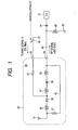
- Fig. 1 is a diagram illustrating a configuration of a circuit from an antenna module to a tuner in a receiver according to an embodiment of the invention.
- Fig. 2 is a diagram illustrating the overall configuration of the receiver.
- the receiver of the embodiment is configured to perform frequency conversion by inputting an RF signal output from an antenna module 20 to a tuner 21, and to perform demodulation by inputting an IF signal obtained by the frequency conversion to a demodulating IC 22.
- the receiver is also configured to allow a processor 23 formed by combination of a CPU, a MPEG decoder, and the like to restore video data and sound data and output the data to a monitor and a speaker not shown in the drawing. From the demodulating IC 22, a tuning signal Vt for determining a tuning frequency in accordance with program selection is transmitted to the antenna module 20.
- the antenna module 20 includes an antenna element 31 and a tunable matching circuit 32.
- the tuning signal Vt DC bias
- the RF signal is output from a second terminal 34 to the tuner 21.
- the antenna element 31 is formed as a helical antenna having a shape in which a radiation conductor 2 is helically wound around an outer periphery of a base substance 1 made of resin.
- a ground for obtaining a ground potential of the tunable matching circuit 32 is removed from just below the antenna element 31.
- the base substance 1 is made of resin, but the invention is not limited to this, and the base substance may be made of a dielectric substance, a magnetic substance, or combined materials of them.
- the base substance may be formed of a film.
- the radiation conductor has a helical structure, but the invention is not limited to this, and the radiation conductor may be formed in a monopole shape or a loop shape.
- one end of the inductor 35 is connected to an output terminal of the antenna element 31, and the other end of the inductor 35 is connected to an anode of one side varactor diode 36.
- a cathode of the one side varactor diode 36 is connected in series to a cathode of the other side varactor diode 38 via an inductor 37.
- An anode of the other side varactor diode 38 is connected to one end of an inductor 39, and the other end of the inductor 39 is connected to the second terminal 34.
- one end of a grounding resistor 41 having high impedance with respect to high frequency is connected to the one end of the inductor 35.
- an inductor having high impedance with respect to a high frequency instead of the grounding resistor 41 may be used.
- the other end of the grounding resistor 41 is connected to the second terminal 34 via a ground line (or pattern) 42.
- the second terminal 34 is connected to an input terminal of the tuner 21 via a transmission line 43 formed on a set substrate having the antenna apparatus attached thereto. Between the second terminal 34 and the tuner 21, a DC cut capacitor 44 is provided.
- the transmission line 43 is connected to a ground 46 on the set substrate side via an inductor 45. Specifically, a ground potential serving as a reference electric potential of the one side varactor diode 36 is applied from the ground 46 on the set substrate side via the ground line 42 on the antenna apparatus side and the transmission line 43 on the set substrate side. In addition, a ground potential of the other side varactor diode 38 is applied via the transmission line 43 on the set substrate side.
- a cathode side connecting point between one side varactor diode 36 and the other side varactor diode 38 is connected to the first terminal 33 via a bias resistor 47.
- the first terminal 33 is connected to a variable DC output circuit 48 set on the set substrate side.
- the variable DC output circuit 48 generates a DC voltage having a magnitude based on a channel select signal given from the demodulating IC 22, and outputs the DC voltage as a tuning signal Vt.
- the variable DC output circuit 48 may be configured to control the DC bias voltage in a PWM mode.
- the variable DC output circuit 48 may be configured to have a DA converter on a reception circuit side and generate a required DC bias voltage on the basis of digital data input to the DA converter.
- a path for applying the tuning signal Vt to a connecting point between the varactor diodes 36 and 38 on the cathode side and a path for connecting the anode of the varactor diodes 36 and 38 to the ground 46 and transmitting an RF signal to the tuner 21 are separately formed.
- the anode of the one side varactor diode 36 is connected to the set-substrate side ground 46 via the grounding resistor 41, the ground line 42, the transmission line 43, and the inductor 45. Furthermore, the anode of the other side varactor diode 38 is connected to the set-substrate side ground 46 via the transmission line 43 and the inductor 45. Accordingly, the set-substrate side ground 46 applies a DC ground potential to the anodes of the varactor diodes 36 and 38 of the tunable matching circuit 32, and applies a high-frequency ground potential to a tuner side end of the inductor 39 via the inductor 45.
- a DC bias instruction value based on channel selection is given to the variable DC output circuit 48.
- the variable DC output circuit 48 generates a DC bias corresponding to the DC bias instruction value and applies the DC bias as a tuning voltage Vt to the first terminal 33.
- the tuning voltage Vt applied to the first terminal 33 is applied to the cathodes of the varactor diodes 36 and 38 via a voltage applying line separate from the transmission line 43.
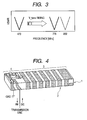
- Fig. 3 is a diagram illustrating relationship between a frequency and a VSWR (Voltage Standing Wave Ratio) when the tuning voltage Vt is varied. As shown in the drawing, the most effective frequency for transferring high frequency energy is varied depending on the tuning voltage Vt.
- VSWR Voltage Standing Wave Ratio
- the tunable matching circuit 32 extracts a frequency component corresponding to a band of the selected channel from the RF signal output from the antenna element 31, and outputs the component from the second terminal 34.
- the RF signal of the selected channel band extracted in the tunable matching circuit 32 is input to the tuner 21 via the transmission line 43.
- the RF signal is converted into an IF signal by frequency conversion in the tuner 21, and is demodulated by the demodulating IC 22.
- video data and sound data is restored from the demodulated signal, and is output to a monitor and a speaker not shown in the drawing.
- the tunable matching circuit 32 is configured to acquire a ground potential from the set substrate side to which the antenna module 20 is attached, and the voltage applying line of the tuning signal Vt which is a DC bias is formed separately from the transmission line 43 for inputting the RF signal to the tuner side.
- the embodiments of the invention can be applied to antenna apparatuses built in small wireless mechanisms such as a cellular phone to receive television signals.
Landscapes
- Engineering & Computer Science (AREA)
- Microelectronics & Electronic Packaging (AREA)
- Input Circuits Of Receivers And Coupling Of Receivers And Audio Equipment (AREA)
- Details Of Aerials (AREA)
- Variable-Direction Aerials And Aerial Arrays (AREA)
Abstract
Provided is an antenna apparatus including: an antenna element (3) having a radiation conductor (2) formed on a surface of a base substance (1); and a matching circuit (32) formed on the base substance (1) to match with the radiation conductor (2) and having a variable capacitor to which a control voltage for controlling capacitance is applied from a reception circuit formed outside the base substance (1). In the antenna, a direct-current ground potential of the matching circuit (32) is applied via a transmission line (43) for transmitting an RF signal output from the matching circuit (32) to the reception circuit.
Description
- The present application contains subject matter related to Japanese Patent Application No.
2007-290363 - The present invention relates to an antenna apparatus used in a cellular phone and the like to receive a television signal.
- Now days, antenna apparatuses for a television device built in a mobile device such as a cellular phone have been developed. Since a broadcast band for television broadcast signals is a wide band (for example, 470 MHz to 770 MHz in Japan), a wideband antenna apparatus is needed to correspond to the wide band when one antenna is intended to be used. For example, in an antenna apparatus disclosed in Japanese Unexamined Patent Application Publication No.
H06-314982 -
Fig. 4 is an exterior diagram illustrating an antenna apparatus having a tunable matching circuit tuning to the used frequency and functioning as a matching circuit.Fig. 5 is a diagram illustrating a configuration of an antenna module of the antenna apparatus shown inFig. 4 . As shown inFig. 4 , the antenna apparatus includes an antenna element (helical antenna) 3 formed by winding aradiation conductor 2 in a helical shape around an outer periphery of a base substance 1 made of resin and a tunable matchingcircuit 4 capable of controlling a used frequency band with a signal from a tuner. A ground surface GND for providing a ground potential of thetunable matching circuit 4 is formed just below theantenna element 3. Thetunable matching circuit 4 includes a resonant circuit formed ofvaractor diodes inductors Fig. 5 . An anode of oneside varactor diode 11 connected to theantenna element 3 is connected via aresistor 16 to a ground GND formed just below the antenna. In addition, an anode of the otherside varactor diode 12 and one end of aninductor 15 is connected to the ground GND formed just below the antenna via aninductor 17. Furthermore, one end of a bypass line L for applying a tuning signal Vt is connected to cathodes of thevaractor diodes inductor 15 is connected to a tuner via aDC cut capacitor 18. - In the antenna apparatus configured as described above, capacitances of the
varactor diodes varactor diodes antenna element 3, and is transmitted to the tuner. - However, in the antenna apparatus, to obtain a stable ground potential by a
tunable matching circuit 4, the ground GND is formed just below the antenna. Thus, the ground GND becomes a factor of lowering a gain and a radiation efficiency of the antenna, thereby deteriorating antenna performance. - It is desirable to provide an antenna apparatus free from an influence of the ground line on an antenna element by removing a ground surface for applying a ground potential to a tunable matching circuit from just below the antenna.
- According to an aspect of the invention, the antenna apparatus includes: an antenna element having a radiation conductor formed on a surface of a base substance; and a matching circuit formed on the base substance to match with the radiation conductor and having a variable capacitor to which a control voltage for controlling capacitance is applied from a reception circuit formed outside the base substance. In the antenna apparatus, a ground potential of the matching circuit is applied via a transmission line for transmitting an RF signal output from the matching circuit to the reception circuit.
- With such a configuration, since the ground potential of the matching circuit is applied via the transmission line for transmitting the RF signal output from the matching circuit to the reception circuit, it is possible to remove a ground surface for applying a ground potential to the matching circuit of the antenna from just below the antenna. Thus, it is possible to prevent the antenna element from being affected by a ground line.
- In the antenna apparatus according to the aspect of the invention, it is preferred that an inductor be connected in series between the transmission line and a ground of the reception circuit on the reception circuit side.
- With such a configuration, since the inductor is connected in series between the transmission line and the ground of the reception circuit, it is possible to provide a DC ground and a high frequency ground on the reception circuit side to the matching circuit.
- In the antenna apparatus according to the aspect of the invention, it is preferred that the voltage applied to the variable capacitor of the matching circuit be supplied via a line separate from the transmission line.
- With such a configuration, since the voltage applied to the variable capacitor of the matching circuit is supplied via the line separate from the transmission line, it is possible to provide a DC ground and a high frequency ground via the transmission line to the matching circuit of the antenna.
- In the antenna apparatus according to the aspect of the invention, it is preferred that the matching circuit have two variable capacitors connected to each other in series and have a resistor or an inductor between the transmission line and a radiation-conductor side end of the variable capacitor close to the radiation conductor.
- According to the aspect of the invention, it is possible to remove a ground surface for applying a ground potential to the tunable matching circuit of the antenna from the antenna side. Thus, it is possible to prevent the antenna element from being affected by a ground line.
-
-
Fig. 1 is a diagram illustrating a configuration of a circuit from an antenna module to a tuner in a receiver according to an embodiment of the invention. -
Fig. 2 is a diagram illustrating the overall configuration of the receiver according to the embodiment. -
Fig. 3 is a diagram illustrating relationship between a frequency and a VSWR when a tuning voltage Vt is varied. -
Fig. 4 is a diagram illustrating an exterior of an antenna apparatus having a tunable matching circuit. -
Fig. 5 is a diagram illustrating a configuration of an antenna module of the antenna apparatus shown inFig. 4 . - Hereinafter, an embodiment of the invention will be described in detail with reference to the attached drawings.
-
Fig. 1 is a diagram illustrating a configuration of a circuit from an antenna module to a tuner in a receiver according to an embodiment of the invention.Fig. 2 is a diagram illustrating the overall configuration of the receiver. - As shown in
Fig. 2 , the receiver of the embodiment is configured to perform frequency conversion by inputting an RF signal output from anantenna module 20 to atuner 21, and to perform demodulation by inputting an IF signal obtained by the frequency conversion to a demodulatingIC 22. The receiver is also configured to allow aprocessor 23 formed by combination of a CPU, a MPEG decoder, and the like to restore video data and sound data and output the data to a monitor and a speaker not shown in the drawing. From the demodulatingIC 22, a tuning signal Vt for determining a tuning frequency in accordance with program selection is transmitted to theantenna module 20. - The
antenna module 20, as shown inFig. 1 , includes anantenna element 31 and atunable matching circuit 32. In the module, the tuning signal Vt (DC bias) is applied from the demodulatingIC 22 to afirst terminal 33, and the RF signal is output from asecond terminal 34 to thetuner 21. - Similarly to the antenna apparatus shown in
Fig. 4 , theantenna element 31 is formed as a helical antenna having a shape in which aradiation conductor 2 is helically wound around an outer periphery of a base substance 1 made of resin. However, in the embodiment, a ground for obtaining a ground potential of thetunable matching circuit 32 is removed from just below theantenna element 31. In the embodiment, the base substance 1 is made of resin, but the invention is not limited to this, and the base substance may be made of a dielectric substance, a magnetic substance, or combined materials of them. In addition, the base substance may be formed of a film. Furthermore, the radiation conductor has a helical structure, but the invention is not limited to this, and the radiation conductor may be formed in a monopole shape or a loop shape. - In the
tunable matching circuit 32, one end of theinductor 35 is connected to an output terminal of theantenna element 31, and the other end of theinductor 35 is connected to an anode of oneside varactor diode 36. A cathode of the oneside varactor diode 36 is connected in series to a cathode of the otherside varactor diode 38 via aninductor 37. An anode of the otherside varactor diode 38 is connected to one end of aninductor 39, and the other end of theinductor 39 is connected to thesecond terminal 34. To apply a ground potential to the anode of thevaractor diode 36, one end of agrounding resistor 41 having high impedance with respect to high frequency (not less than the lower limit of used frequency band) is connected to the one end of theinductor 35. Furthermore, an inductor having high impedance with respect to a high frequency instead of thegrounding resistor 41 may be used. In the embodiment, the other end of thegrounding resistor 41 is connected to thesecond terminal 34 via a ground line (or pattern) 42. Thesecond terminal 34 is connected to an input terminal of thetuner 21 via atransmission line 43 formed on a set substrate having the antenna apparatus attached thereto. Between thesecond terminal 34 and thetuner 21, aDC cut capacitor 44 is provided. Thetransmission line 43 is connected to aground 46 on the set substrate side via aninductor 45. Specifically, a ground potential serving as a reference electric potential of the oneside varactor diode 36 is applied from theground 46 on the set substrate side via theground line 42 on the antenna apparatus side and thetransmission line 43 on the set substrate side. In addition, a ground potential of the otherside varactor diode 38 is applied via thetransmission line 43 on the set substrate side. - Furthermore, in the
tunable matching circuit 32, a cathode side connecting point between oneside varactor diode 36 and the otherside varactor diode 38 is connected to thefirst terminal 33 via abias resistor 47. Thefirst terminal 33 is connected to a variableDC output circuit 48 set on the set substrate side. The variableDC output circuit 48 generates a DC voltage having a magnitude based on a channel select signal given from thedemodulating IC 22, and outputs the DC voltage as a tuning signal Vt. For example, the variableDC output circuit 48 may be configured to control the DC bias voltage in a PWM mode. Alternatively, the variableDC output circuit 48 may be configured to have a DA converter on a reception circuit side and generate a required DC bias voltage on the basis of digital data input to the DA converter. - In the embodiment, a path for applying the tuning signal Vt to a connecting point between the
varactor diodes varactor diodes ground 46 and transmitting an RF signal to thetuner 21 are separately formed. - In the embodiment configured as described above, the anode of the one
side varactor diode 36 is connected to the set-substrate side ground 46 via thegrounding resistor 41, theground line 42, thetransmission line 43, and theinductor 45. Furthermore, the anode of the otherside varactor diode 38 is connected to the set-substrate side ground 46 via thetransmission line 43 and theinductor 45. Accordingly, the set-substrate side ground 46 applies a DC ground potential to the anodes of thevaractor diodes tunable matching circuit 32, and applies a high-frequency ground potential to a tuner side end of theinductor 39 via theinductor 45. - A DC bias instruction value based on channel selection is given to the variable
DC output circuit 48. The variableDC output circuit 48 generates a DC bias corresponding to the DC bias instruction value and applies the DC bias as a tuning voltage Vt to thefirst terminal 33. The tuning voltage Vt applied to thefirst terminal 33 is applied to the cathodes of thevaractor diodes transmission line 43.Fig. 3 is a diagram illustrating relationship between a frequency and a VSWR (Voltage Standing Wave Ratio) when the tuning voltage Vt is varied. As shown in the drawing, the most effective frequency for transferring high frequency energy is varied depending on the tuning voltage Vt. Accordingly, by controlling the tuning voltage Vt in accordance with channel selection, it is possible to most effectively apply high frequency energy. Thetunable matching circuit 32 extracts a frequency component corresponding to a band of the selected channel from the RF signal output from theantenna element 31, and outputs the component from thesecond terminal 34. The RF signal of the selected channel band extracted in thetunable matching circuit 32 is input to thetuner 21 via thetransmission line 43. The RF signal is converted into an IF signal by frequency conversion in thetuner 21, and is demodulated by thedemodulating IC 22. In theprocessor 23, video data and sound data is restored from the demodulated signal, and is output to a monitor and a speaker not shown in the drawing. - In the embodiment, the
tunable matching circuit 32 is configured to acquire a ground potential from the set substrate side to which theantenna module 20 is attached, and the voltage applying line of the tuning signal Vt which is a DC bias is formed separately from thetransmission line 43 for inputting the RF signal to the tuner side. With such a configuration, it is possible to acquire a DC ground and an RF ground necessary for thetunable matching circuit 32 of the antenna apparatus from the set substrate side, and it is possible to remove a ground surface from just below theantenna element 31. Thus, it is possible to embody an antenna apparatus free from an influence of the ground line on the antenna element. - The embodiments of the invention can be applied to antenna apparatuses built in small wireless mechanisms such as a cellular phone to receive television signals.
- It should be understood by those skilled in the art that various modifications, combinations, sub-combinations and alterations may occur depending on design requirements and other factors insofar as they are within the scope of the appended claims of the equivalents thereof.
Claims (4)
- An antenna apparatus comprising:an antenna element (3) having a radiation conductor (2) formed on a surface of a base substance (1); anda matching circuit (32) formed on the base substance (1) to match with the radiation conductor (2) and having a variable capacitor to which a control voltage for controlling capacitance is applied from a reception circuit formed outside the base substance (1),wherein a direct-current ground potential of the matching circuit (32) is applied via a transmission line (43) for transmitting an RF signal output from the matching circuit (32) to the reception circuit.
- The antenna apparatus according to claim 1, wherein an inductor is connected between the transmission line (43) and a ground of the reception circuit on the reception circuit side.
- The antenna apparatus according to claim 1 or 2, wherein the voltage applied to the variable capacitor of the matching circuit (32) is supplied via a line separate from the transmission line (43).
- The antenna apparatus according to any one of claims 1 to 3, wherein the matching circuit (32) has a plurality of the variable capacitors connected to each other in series and has a resistor or an inductor between the transmission line (43) and a radiation-conductor side end of the variable capacitor close to the radiation conductor (2).
Applications Claiming Priority (1)
| Application Number | Priority Date | Filing Date | Title |
|---|---|---|---|
| JP2007290363A JP2009118292A (en) | 2007-11-08 | 2007-11-08 | Antenna apparatus |
Publications (1)
| Publication Number | Publication Date |
|---|---|
| EP2063486A1 true EP2063486A1 (en) | 2009-05-27 |
Family
ID=40497438
Family Applications (1)
| Application Number | Title | Priority Date | Filing Date |
|---|---|---|---|
| EP08019387A Withdrawn EP2063486A1 (en) | 2007-11-08 | 2008-11-05 | Antenna apparatus |
Country Status (2)
| Country | Link |
|---|---|
| EP (1) | EP2063486A1 (en) |
| JP (1) | JP2009118292A (en) |
Families Citing this family (1)
| Publication number | Priority date | Publication date | Assignee | Title |
|---|---|---|---|---|
| US8413094B2 (en) * | 2010-10-05 | 2013-04-02 | International Business Machines Corporation | Structure, design structure and process for increasing magnitude of device threshold voltage for low power applications |
Citations (6)
| Publication number | Priority date | Publication date | Assignee | Title |
|---|---|---|---|---|
| JPH06314982A (en) | 1993-04-30 | 1994-11-08 | Kenwood Corp | Antenna |
| JPH10209897A (en) * | 1997-01-20 | 1998-08-07 | Harada Ind Co Ltd | Tunable antenna device |
| EP1231674A2 (en) * | 2001-02-07 | 2002-08-14 | Matsushita Electric Industrial Co., Ltd. | Antenna device |
| EP1471597A1 (en) * | 2003-04-22 | 2004-10-27 | Alps Electric Co., Ltd. | Card with built-in antenna |
| EP1617564A1 (en) * | 2003-04-18 | 2006-01-18 | Yokowo Co., Ltd | Variable tuning antenna and mobile wireless device using same |
| JP2007290363A (en) | 2006-03-27 | 2007-11-08 | Seiko Epson Corp | Liquid cartridge |
-
2007
- 2007-11-08 JP JP2007290363A patent/JP2009118292A/en not_active Withdrawn
-
2008
- 2008-11-05 EP EP08019387A patent/EP2063486A1/en not_active Withdrawn
Patent Citations (6)
| Publication number | Priority date | Publication date | Assignee | Title |
|---|---|---|---|---|
| JPH06314982A (en) | 1993-04-30 | 1994-11-08 | Kenwood Corp | Antenna |
| JPH10209897A (en) * | 1997-01-20 | 1998-08-07 | Harada Ind Co Ltd | Tunable antenna device |
| EP1231674A2 (en) * | 2001-02-07 | 2002-08-14 | Matsushita Electric Industrial Co., Ltd. | Antenna device |
| EP1617564A1 (en) * | 2003-04-18 | 2006-01-18 | Yokowo Co., Ltd | Variable tuning antenna and mobile wireless device using same |
| EP1471597A1 (en) * | 2003-04-22 | 2004-10-27 | Alps Electric Co., Ltd. | Card with built-in antenna |
| JP2007290363A (en) | 2006-03-27 | 2007-11-08 | Seiko Epson Corp | Liquid cartridge |
Also Published As
| Publication number | Publication date |
|---|---|
| JP2009118292A (en) | 2009-05-28 |
Similar Documents
| Publication | Publication Date | Title |
|---|---|---|
| US11469740B2 (en) | Adaptive self-tunable antenna system and method | |
| US6606069B2 (en) | Antenna device | |
| US7557773B2 (en) | Variable tuning antenna and mobile wireless device using same | |
| KR101122851B1 (en) | Broadcast reception terminal apparatus | |
| JP4959956B2 (en) | antenna | |
| EP1983605A1 (en) | Antenna device | |
| EP2128924A1 (en) | Antenna apparatus | |
| EP2139065A1 (en) | Antenna device | |
| JP2008259039A (en) | Antenna device | |
| TWI322617B (en) | A tv tuner and the manufacturing method thereof | |
| JP3829805B2 (en) | Planar antenna | |
| JP2009044561A (en) | Antenna matching circuit | |
| US20060139227A1 (en) | Antenna device having enhanced reception sensitivity in wide bands | |
| JP5003628B2 (en) | Tunable antenna and receiving device equipped with tunable antenna | |
| JP2009118292A (en) | Antenna apparatus | |
| EP1788662A1 (en) | Wideband receiving antenna device | |
| US7345651B2 (en) | Antenna | |
| EP1641072B1 (en) | Antenna with variable directivity pattern | |
| Kim et al. | Tunable internal loop antenna for DVB-H service | |
| JP2009253685A (en) | Tunable antenna module, and wireless apparatus | |
| JP2012034379A (en) | Radio unit and radio device | |
| JP2009272981A (en) | Receiver and mobile terminal device with the same | |
| JP2012186585A (en) | Television tuner | |
| JPH07303031A (en) | Electronic tuner |
Legal Events
| Date | Code | Title | Description |
|---|---|---|---|
| PUAI | Public reference made under article 153(3) epc to a published international application that has entered the european phase |
Free format text: ORIGINAL CODE: 0009012 |
|
| AK | Designated contracting states |
Kind code of ref document: A1 Designated state(s): AT BE BG CH CY CZ DE DK EE ES FI FR GB GR HR HU IE IS IT LI LT LU LV MC MT NL NO PL PT RO SE SI SK TR |
|
| AX | Request for extension of the european patent |
Extension state: AL BA MK RS |
|
| 17P | Request for examination filed |
Effective date: 20090715 |
|
| AKX | Designation fees paid |
Designated state(s): DE FR GB IT |
|
| STAA | Information on the status of an ep patent application or granted ep patent |
Free format text: STATUS: THE APPLICATION HAS BEEN WITHDRAWN |
|
| 18W | Application withdrawn |
Effective date: 20140128 |