EP2061083A1 - Organic light emitting display apparatus - Google Patents
Organic light emitting display apparatus Download PDFInfo
- Publication number
- EP2061083A1 EP2061083A1 EP08169186A EP08169186A EP2061083A1 EP 2061083 A1 EP2061083 A1 EP 2061083A1 EP 08169186 A EP08169186 A EP 08169186A EP 08169186 A EP08169186 A EP 08169186A EP 2061083 A1 EP2061083 A1 EP 2061083A1
- Authority
- EP
- European Patent Office
- Prior art keywords
- layer
- conductive layer
- light emitting
- power supply
- organic light
- Prior art date
- Legal status (The legal status is an assumption and is not a legal conclusion. Google has not performed a legal analysis and makes no representation as to the accuracy of the status listed.)
- Granted
Links
Images




Classifications
-
- H—ELECTRICITY
- H05—ELECTRIC TECHNIQUES NOT OTHERWISE PROVIDED FOR
- H05B—ELECTRIC HEATING; ELECTRIC LIGHT SOURCES NOT OTHERWISE PROVIDED FOR; CIRCUIT ARRANGEMENTS FOR ELECTRIC LIGHT SOURCES, IN GENERAL
- H05B33/00—Electroluminescent light sources
- H05B33/12—Light sources with substantially two-dimensional [2D] radiating surfaces
- H05B33/26—Light sources with substantially two-dimensional [2D] radiating surfaces characterised by the composition or arrangement of the conductive material used as an electrode
-
- H—ELECTRICITY
- H05—ELECTRIC TECHNIQUES NOT OTHERWISE PROVIDED FOR
- H05B—ELECTRIC HEATING; ELECTRIC LIGHT SOURCES NOT OTHERWISE PROVIDED FOR; CIRCUIT ARRANGEMENTS FOR ELECTRIC LIGHT SOURCES, IN GENERAL
- H05B33/00—Electroluminescent light sources
- H05B33/10—Apparatus or processes specially adapted to the manufacture of electroluminescent light sources
-
- H—ELECTRICITY
- H10—SEMICONDUCTOR DEVICES; ELECTRIC SOLID-STATE DEVICES NOT OTHERWISE PROVIDED FOR
- H10K—ORGANIC ELECTRIC SOLID-STATE DEVICES
- H10K59/00—Integrated devices, or assemblies of multiple devices, comprising at least one organic light-emitting element covered by group H10K50/00
- H10K59/10—OLED displays
- H10K59/12—Active-matrix OLED [AMOLED] displays
- H10K59/122—Pixel-defining structures or layers, e.g. banks
-
- H—ELECTRICITY
- H10—SEMICONDUCTOR DEVICES; ELECTRIC SOLID-STATE DEVICES NOT OTHERWISE PROVIDED FOR
- H10K—ORGANIC ELECTRIC SOLID-STATE DEVICES
- H10K59/00—Integrated devices, or assemblies of multiple devices, comprising at least one organic light-emitting element covered by group H10K50/00
- H10K59/10—OLED displays
- H10K59/12—Active-matrix OLED [AMOLED] displays
- H10K59/131—Interconnections, e.g. wiring lines or terminals
- H10K59/1315—Interconnections, e.g. wiring lines or terminals comprising structures specially adapted for lowering the resistance
Definitions
- FIG. 1 is a schematic plan view of an organic light emitting display apparatus according to an embodiment.
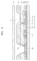
- FIG. 2 is a schematic cross-sectional view taken along line II-II of FIG. 1 , according to an embodiment.
- FIG. 3 is a schematic cross-sectional view for describing a process of manufacturing the organic light emitting display apparatus.
- the sealant 700 and the sealing element 600 may not be formed, or a passivation layer may be formed on the entire surface of the substrate 110.
- the terminal units 192, 320, 420, and 520 are not covered and are exposed by spaces in insulating layers to be described later so as to be connected to other electrical components such as a flexible printing circuit substrate, an IC chip, or the like.
- a buffer layer 120 which may be formed of SiO2, etc., is disposed on the substrate 110.
- a semiconductor layer 130 is disposed on the buffer layer 120.
- the semiconductor layer 130 may be an amorphous silicon layer, a polycrystalline silicon layer, or formed of an organic semiconductor material. Although not shown in FIG. 2 , the semiconductor layer 130 may include source and drain areas doped with a dopant and a channel area.
- An interlayer insulating layer 160 is formed on the gate electrode 150 and may be formed of a material such as silicon oxide, silicon nitride, or the like as a single layer or a multi-layer structure.
- the source and drain electrodes 170 are formed on the interlayer insulating layer 160.
- the source and drain electrodes 170 are electrically connected to the semiconductor layer 130 through contact holes which are formed in the interlayer insulating layer 160 and the gate insulating layer 140, respectively.
- the source and drain electrodes 170 may be formed of a material such as Ti, MoW, Ag, Cu, Al, or the like in consideration of conductivity.
- the source and drain electrodes 170 may be formed as a single layer or a multi-layer structure and, for example, may have a structure in which a Ti layer and an Al layer are stacked.
- the electrode power supply line 190 may be formed of various materials.
- the electrode power supply line 190 supplies an electrical signal to the counter electrode 230 of the organic light emitting device 200 as will be described later and thus is formed of a material having low resistivity and high conductivity such as Ti, MoW, Ag, Cu, Al or the like.
- the electrode power supply line 190 may be formed as a single layer or a multi-layer structure and, for example, may have a structure in which a Ti layer and an A1 layer are stacked.
- the source and drain electrodes 170 and the electrode power supply line 190 may be formed of the same material or may be simultaneously formed together. When the source and drain electrodes 170 and the electrode power supply line 190 are simultaneously formed together, the source and drain electrodes 170 and the electrode power supply line 190 may have the same structure.
- the intermediate layer 220 of the organic light emitting device 200 may be formed of a low or high molecular weight material.
- the intermediate layer 220 may be preferable to have at least one of a hole injection layer (HIL), a hole transport layer (HTL), an emission layer (EML), an electron transport layer (ETL), an electron injection layer (EIL), and the like stacked in a single structure or a multi-layer structure to form the intermediate layer 220.
- HIL hole injection layer
- HTL hole transport layer
- EML emission layer
- ETL electron transport layer
- EIL electron injection layer
- the intermediate layer 220 may be formed of an organic material such as copper phthalocyanine (CuPc), N,N'-Di(naphthalene-1-yl)-N,N'-diphenyl-benzidine (NPB), tris-8-hydroxyquinoline aluminum (Alq3), or the like.
- CuPc copper phthalocyanine
- NPB N,N'-Di(naphthalene-1-yl)-N,N'-diphenyl-benzidine
- Alq3 tris-8-hydroxyquinoline aluminum
- the counter electrode 230 may be a transparent or reflective electrode. If the counter electrode 230 is a transparent electrode, the counter electrode 230 may include a layer formed of a metal having a low work function, i.e., Li, Ca, LiF/Ca, LiF/Al, Al, Ag, Mg, or a combination thereof, and a transparent conductive layer formed of ITO, IZO, ZnO, or In 2 O 3 . If the counter electrode 230 is a reflective electrode, the counter electrode 230 may be formed of Li, Ca, LiF/Ca, LiF/Al, Al, Ag, Mg, or a combination thereof. However, the counter electrode 230 is not limited to these structures and materials, and thus, may be modified into various forms.
Landscapes
- Engineering & Computer Science (AREA)
- Microelectronics & Electronic Packaging (AREA)
- Manufacturing & Machinery (AREA)
- Electroluminescent Light Sources (AREA)
- Devices For Indicating Variable Information By Combining Individual Elements (AREA)
Abstract
Description
- The present invention relates to an organic light emitting display apparatus, and more particularly, to an organic light emitting display apparatus that resists corrosion during a manufacturing process thereof, and the organic light emitting display apparatus can have a remarkably increased yield.
- Generally, organic light emitting display apparatuses refer to display apparatuses including organic light emitting devices. The organic light emitting devices include a pixel electrode, a counter electrode disposed opposite the pixel electrode, and an intermediate layer interposed between the pixel electrode and the counter electrode and including a light emitting layer.
- An organic light emitting display apparatus can be classified as an active matrix display or a passive matrix display according to a driving method of the organic light emitting devices. In an active matrix display apparatus, a thin film transistor (TFT) of each of a plurality of sub-pixels controls the emission of light from the sub-pixel. In a passive matrix display apparatus, a plurality of electrodes arranged in a matrix shape controls the emission of light from a plurality of sub-pixels. In the case of the active matrix display apparatus, counter electrodes of a plurality of sub-pixels are generally formed as one body and contact an electrode power supply line positioned outside a display area.
- The electrode power supply line is covered by an insulating layer that exposes at least a part of the electrode power supply line. The counter electrode contacts the exposed part of the electrode power supply line. However, before forming the counter electrode to contact the electrode power supply line during the manufacturing thereof, a process of exposing a part of the electrode power supply line outside the insulating layer is performed. Thus, the surface of the electrode power supply line is oxidized during the exposing process. As a result, contact resistance is increased in the subsequently-formed structure in which the electrode power supply line contacts with counter electrode.
- One aspect is an organic light emitting display apparatus including a substrate having a display area, a thin film transistor (TFT) disposed inside the display area of the substrate, an electrode power supply line disposed outside the display area of the substrate, a pixel electrode disposed inside the display area of the substrate and electrically connected to the thin film transistor, an auxiliary conductive layer contacting the electrode power supply line, a pixel defining layer exposing the pixel electrode, covering the auxiliary conductive layer, and exposing the electrode power supply line, an intermediate layer disposed on the pixel electrode and including an emitting layer, and a counter electrode disposed on the intermediate layer and extending outside the display area of the substrate to contact the electrode power supply line.
- Another aspect is an organic light emitting display apparatus, including a substrate, a conductive layer disposed on the substrate, an insulating layer covering a portion of the conductive layer so as to expose another portion of the conductive layer, and a terminal unit extending from the conductive layer toward an edge of the substrate, where the terminal unit and the conductive layer that is exposed by the insulating layer are formed of the same material.
- The above and other features and advantages will become more apparent through description of exemplary embodiments with reference to the attached drawings in which:
-
FIG. 1 is a schematic plan view of an organic light emitting display apparatus according to an embodiment; -
FIG. 2 is a schematic cross-sectional view taken along line II-II ofFIG. 1 , according to an embodiment; -
FIG. 3 is a schematic cross-sectional view for describing a process of manufacturing the organic light emitting display apparatus ofFIG. 2 , according to an embodiment; -
FIG. 4 is a schematic cross-sectional view of a portion of an organic light emitting display apparatus; and -
FIG. 5 is a schematic cross-sectional view for describing a process of manufacturing the organic light emitting display apparatus ofFIG. 4 . - Embodiments will now be described in detail with reference to the attached drawings.
-
FIG. 1 is a schematic plan view of an organic light emitting display apparatus according to an embodiment.FIG. 2 is a schematic cross-sectional view taken along line II-II ofFIG. 1 , according to an embodiment.FIG. 3 is a schematic cross-sectional view for describing a process of manufacturing the organic light emitting display apparatus. - Referring to
FIGS. 1 through 3 , the organic light emitting display apparatus shown includes asubstrate 110. Thesubstrate 110 may be formed of various materials such as glass, a metal, plastic or the like. Thesubstrate 110 has adisplay area 100 where display devices are disposed for displaying images. Thedisplay area 100 includes an organiclight emitting device 200 including a pixel electrode 210 (seeFIG. 2 ), a counter electrode 230 (seeFIG. 2 ) disposed opposite thepixel electrode 210, and anintermediate layer 220 including at least an emitting layer interposed between thepixel electrode 210 and thecounter electrode 230. - In addition to the organic
light emitting device 200 of thedisplay area 100, a verticalcircuit driving unit 400 and a horizontalcircuit driving unit 500 that are disposed outside thedisplay area 100, apower wiring unit 300 to which a plurality ofpower supply lines 310 supplying power to thedisplay area 100 are electrically connected, an electrodepower supply line 190 supplying power to thecounter electrode 230, andterminal units substrate 100. Asealant 700 may be applied on edges of thesubstrate 110, so that a sealing element 600 (seeFIG. 2 ) seals thedisplay area 100. Alternatively, thesealant 700 and thesealing element 600 may not be formed, or a passivation layer may be formed on the entire surface of thesubstrate 110. Theterminal units - Structures of the
display area 100 and the organiclight emitting device 200 will now be described in detail with reference toFIG. 2 . - A first thin film transistor TFT1 is disposed in the
display area 100 on thesubstrate 110. The electrodepower supply line 190 is disposed outside thedisplay area 100 on thesubstrate 110. A second TFT TFT2 included in the verticalcircuit driving unit 400 may be disposed outside thedisplay area 100 on thesubstrate 110. The structure and components of the organiclight emitting device 200 will now be described in more detail. - A
buffer layer 120, which may be formed of SiO2, etc., is disposed on thesubstrate 110. Asemiconductor layer 130 is disposed on thebuffer layer 120. Thesemiconductor layer 130 may be an amorphous silicon layer, a polycrystalline silicon layer, or formed of an organic semiconductor material. Although not shown inFIG. 2 , thesemiconductor layer 130 may include source and drain areas doped with a dopant and a channel area. - A
gate electrode 150 is formed above thesemiconductor layer 130, and source anddrain electrodes 170 electrically communicate with each other according to a signal applied to thegate electrode 150. Thegate electrode 150 may be formed of a material such as MoW, Ag, Cu, Al, or the like, in consideration of, for example, adherence to an adjacent layer, planarizing, and machining of a surface of a layer stacked on thegate electrode 150. In the some embodiments, agate insulating layer 140 formed of SiO2 is interposed between thesemiconductor layer 130 and thegate electrode 150 in order to provide insulation between thesemiconductor layer 130 and thegate electrode 150. - An
interlayer insulating layer 160 is formed on thegate electrode 150 and may be formed of a material such as silicon oxide, silicon nitride, or the like as a single layer or a multi-layer structure. The source anddrain electrodes 170 are formed on theinterlayer insulating layer 160. The source anddrain electrodes 170 are electrically connected to thesemiconductor layer 130 through contact holes which are formed in theinterlayer insulating layer 160 and thegate insulating layer 140, respectively. - The source and
drain electrodes 170 may be formed of a material such as Ti, MoW, Ag, Cu, Al, or the like in consideration of conductivity. The source anddrain electrodes 170 may be formed as a single layer or a multi-layer structure and, for example, may have a structure in which a Ti layer and an Al layer are stacked. - The electrode
power supply line 190 is disposed outside thedisplay area 100. Referring toFIG. 2 , the electrodepower supply line 190 is disposed on theinterlayer insulating layer 160 on which the source anddrain electrodes 170 of the first TFT TFT1 are disposed. That is, the electrodepower supply line 190 may be simultaneously formed together with the source anddrain electrodes 170 of the first TFT TFT1. However, the present invention is not limited thereto. That is, the electrodepower supply line 190 may be formed on a layer on which thegate electrode 150 of the first TFT TFT1 is formed or may be formed irrespective of positions of electrodes of the first TFT TFT1. For convenience of explanation, however, the electrodepower supply line 190 is formed on theinterlayer insulating layer 160 on which the source anddrain electrodes 170 are disposed. - The electrode
power supply line 190 may be formed of various materials. The electrodepower supply line 190 supplies an electrical signal to thecounter electrode 230 of the organiclight emitting device 200 as will be described later and thus is formed of a material having low resistivity and high conductivity such as Ti, MoW, Ag, Cu, Al or the like. The electrodepower supply line 190 may be formed as a single layer or a multi-layer structure and, for example, may have a structure in which a Ti layer and an A1 layer are stacked. As described above, the source anddrain electrodes 170 and the electrodepower supply line 190 may be formed of the same material or may be simultaneously formed together. When the source anddrain electrodes 170 and the electrodepower supply line 190 are simultaneously formed together, the source anddrain electrodes 170 and the electrodepower supply line 190 may have the same structure. - The electrode
power supply line 190 supplies power to thecounter electrode 230 as will be described later. Theterminal unit 192 is extended from the electrodepower supply line 190 toward an edge of thesubstrate 110. Power is supplied to the electrodepower supply line 190 through theterminal unit 192 and is supplied to thecounter electrode 230 through the electrodepower supply line 190. Theterminal unit 192 and the electrodepower supply line 190 may be simultaneously formed together, and accordingly, may be formed of the same material. When theterminal unit 192 and the electrodepower supply line 190 are simultaneously formed together, structures thereof are the same or similar. In some embodiments, theterminal unit 192 and/or the electrodepower supply line 190 may include a layer formed of Al in consideration of conductivity. - A first insulating
layer 181 is formed above the first TFT TFT1 to operate as a passivation layer so as to protect the first TFT TFT1. The first insulatinglayer 181 may be formed of various materials, i.e., an inorganic material, such as silicon oxide, silicon nitride, or silicon oxynitride, which can provide a high level of protection for the first TFT TFT1. The first insulatinglayer 181 is formed as a single layer inFIG. 2 ; however, the it is not limited thereto and the first insulatinglayer 181 may be formed as a multi-layer structure. The first insulatinglayer 181 is formed so as to expose at least a part of the electrodepower supply line 190.FIG. 2 illustrates a structure in which the first insulatinglayer 181 covers edge portions of the electrodepower supply line 190. - A second insulating
layer 182 functions as a planarizing layer on the first insulatinglayer 181. The secondinsulating layer 182 may be formed of an organic material, e.g., acryl, BCB, photoacryl, or the like. The secondinsulating layer 182 is illustrated as a single layer inFIG. 2 . However, it is not limited thereto and the second insulatinglayer 182 may be formed as a multi-layer structure. The secondinsulating layer 182 is formed so as to expose at least a part of the electrodepower supply line 190. - The organic
light emitting device 200 is disposed on the second insulatinglayer 182 and includes thepixel electrode 210, thecounter electrode 230, and theintermediate layer 220 interposed between thepixel electrode 210 and thecounter electrode 230. The organiclight emitting device 200 will now be described in detail. - In the
display area 100, openings are formed in the first and second insulatinglayers electrodes 170 of the first TFT TFT1. Thepixel electrode 210 is disposed on thedisplay area 100 of thesubstrate 110, i.e., on the second insulatinglayer 182 and contacts at least one of the source and drainelectrodes 170 through the openings so as to be electrically connected to the first TFT TFT1. Thepixel electrode 210 may be a transparent electrode or a reflective electrode. If thepixel electrode 210 is a transparent electrode, thepixel electrode 210 may be formed of, for example, indium tin oxide (ITO), indium zinc oxide (IZO), ZnO, or In2O3. If thepixel electrode 210 is a reflective electrode, thepixel electrode 210 may, for example include a reflective layer formed of Ag, Mg, Al, Pt, Pd, Au, Ni, Nd, Ir, Cr, or a combination thereof, and a layer formed of ITO, IZO, ZnO, or In2O3. However, thepixel electrode 210 is not limited thereto, and thepixel electrode 210 may be formed of various materials, and also, may be formed as a single layer or a multi-layer structure. - A third insulating
layer 183 is disposed on the second insulatinglayer 182. In other words, the third insulatinglayer 183 is formed so as to cover the second insulatinglayer 182. The thirdinsulating layer 183 operates as a pixel defining layer by having openings corresponding to a plurality of sub-pixels, which expose at least a part of thepixel electrode 210. For example, a central portion or the whole portion of thepixel electrode 210 may be exposed. Referring toFIG. 2 , the third insulatinglayer 183 increases a distance between the end of thepixel electrode 210 and thecounter electrode 230. This is beneficial in preventing arcing between thepixel electrode 210 and thecounter electrode 230. The thirdinsulating layer 183 is disposed on the second insulatinglayer 182, and also may be disposed outside thedisplay area 100 as illustrated inFIG. 2 . That is, the third insulatinglayer 183 may be disposed both over and outside thedisplay area 100 of thesubstrate 110. Also, the third insulatinglayer 183 ofFIG. 2 exposes at least a part of the electrodepower supply line 190. - An auxiliary
conductive layer 190a is disposed so as to contact the electrodepower supply line 190 at a side of the electrodepower supply line 190. The auxiliaryconductive layer 190a contacts the electrodepower supply line 190 so as to establish a lower conductive path and reduce IR drop through the electrodepower supply line 190. The auxiliaryconductive layer 190a may be disposed outside thedisplay area 100 of thesubstrate 110. Referring toFIG. 2 , a part of the auxiliaryconductive layer 190a may be disposed on the same layer on which thepixel electrode 210 is disposed. InFIG. 2 , the auxiliaryconductive layer 190a is disposed on the second insulatinglayer 182 and the electrodepower supply line 190. In this case, the auxiliaryconductive layer 190a may be formed of the same material as that of thepixel electrode 210. The auxiliaryconductive layer 190a and thepixel electrode 210 may be simultaneously formed together. In this case, the auxiliaryconductive layer 190a and thepixel electrode 210 may have the same structure. The auxiliaryconductive layer 190a is covered by the third insulatinglayer 183, and accordingly, the auxiliaryconductive layer 190a is not exposed outside the third insulatinglayer 183. - The
intermediate layer 220 of the organiclight emitting device 200 may be formed of a low or high molecular weight material. When theintermediate layer 220 is formed of a low molecular weight material, it may be preferable to have at least one of a hole injection layer (HIL), a hole transport layer (HTL), an emission layer (EML), an electron transport layer (ETL), an electron injection layer (EIL), and the like stacked in a single structure or a multi-layer structure to form theintermediate layer 220. Alternatively, theintermediate layer 220 may be formed of an organic material such as copper phthalocyanine (CuPc), N,N'-Di(naphthalene-1-yl)-N,N'-diphenyl-benzidine (NPB), tris-8-hydroxyquinoline aluminum (Alq3), or the like. These layers may be formed, for example, using a vacuum deposition method. - When the
intermediate layer 220 is formed of a high molecular weight material, theintermediate layer 200 it may be preferable to have a structure in which an HTL and an EML are stacked. The HTL may be formed of PEDOT, and the EML may be formed of Poly-Phenylenevinylene (PPV)-family and Polyfluorene-family high molecular weight materials using a screen printing method, an inkjet printing method, or the like. However, theintermediate layer 220 is not limited to this structure, and may have various other structures. - The
counter electrode 230 may be disposed on theintermediate layer 220, over thedisplay area 100 as illustrated inFIG. 2 . Thecounter electrode 230 extends outside thedisplay area 100 and contacts the electrodepower supply line 190 disposed outside thedisplay area 100 to receive power from the electrodepower supply line 190. That is, thecounter electrode 230 extends outside thedisplay area 100 of thesubstrate 110 over the third insulatinglayer 183 and the electrodepower supply line 190 which is exposed by the third insulatinglayer 183. - The
counter electrode 230 may be a transparent or reflective electrode. If thecounter electrode 230 is a transparent electrode, thecounter electrode 230 may include a layer formed of a metal having a low work function, i.e., Li, Ca, LiF/Ca, LiF/Al, Al, Ag, Mg, or a combination thereof, and a transparent conductive layer formed of ITO, IZO, ZnO, or In2O3. If thecounter electrode 230 is a reflective electrode, thecounter electrode 230 may be formed of Li, Ca, LiF/Ca, LiF/Al, Al, Ag, Mg, or a combination thereof. However, thecounter electrode 230 is not limited to these structures and materials, and thus, may be modified into various forms. -
FIG. 3 is a schematic cross-sectional view for describing a process of manufacturing the organic light emitting display apparatus according to one embodiment.FIG. 3 illustrates the organic light emitting display apparatus before forming theintermediate layer 220 and thecounter electrode 230. - As described above, the third insulating
layer 183 has an opening exposing at least a part of thepixel electrode 210 and an opening exposing at least a part of the electrodepower supply line 190, and covers the auxiliaryconductive layer 190a. In an embodiment of a process to form the third insulatinglayer 183, an insulating layer is formed on the entire surface of thesubstrate 110. Then, exposing, developing, and etching processes are performed on the insulating layer using photoresist. Finally, a washing process is performed on the insulating layer using deionized (DI) water. In these manufacturing steps, since the auxiliaryconductive layer 190a is covered by the third insulatinglayer 183, the electrodepower supply line 190, theterminal unit 192, and the auxiliaryconductive layer 190a are not damaged. -
FIG. 4 is a schematic cross-sectional view of an embodiment of a portion of an organic light emitting display apparatus.FIG. 5 is a schematic cross-sectional view for describing a process of manufacturing the organic light emitting display apparatus ofFIG. 4 . Referring toFIGS. 4 and5 , an auxiliaryconductive layer 190b is disposed on an electrodepower supply line 190, and a thirdinsulating layer 183 is formed so as to expose the auxiliaryconductive layer 190b. Acounter electrode 230 contacts the auxiliaryconductive layer 190b so as to be electrically connected to the electrodepower supply line 190 via the auxiliaryconductive layer 190b. - In the organic light emitting display apparatus illustrated in
FIGS. 4 and5 , the auxiliaryconductive layer 190b is exposed in a process of forming the third insulatinglayer 183 and the subsequent processes. In this case, since a terminal unit connected to the electrodepower supply line 190 is exposed outside the third insulatinglayer 183, the auxiliaryconductive layer 190b or the terminal unit may be damaged in the process of forming the third insulatinglayer 183 and the subsequent processes. - In more detail, a developing process of the third insulating
layer 183 using photoresist and stripping and/or washing processes of the photoresist are performed using a wet process. In the above processes, the auxiliaryconductive layer 190b and the terminal unit, which are respectively formed of different materials, are exposed by an alkali solution used in the wet process. At this time, a potential difference is generated between the auxiliaryconductive layer 190b and the terminal unit due to a galvanic phenomenon, so that at least one of the auxiliaryconductive layer 190b and the terminal unit is greatly damaged. For example, if apixel electrode 210 includes a layer formed of ITO, and the auxiliaryconductive layer 190b is formed of the same material as that of thepixel electrode 210 and thus also includes a layer formed of ITO, the terminal unit includes a layer formed of Al and the electrodepower supply line 190 is formed of the same material as that of the terminal unit and thus also includes a layer formed of Al, the layer formed of Al is oxidized and the layer formed of ITO is reduced, thereby damaging the layer formed of Al. As a result, resistance of the Al layer is sharply increased due to oxidization of the Al layer, thereby causing defect of the organic light emitting display apparatus. - However, in the organic light emitting display apparatus according to the embodiment as shown in
FIGS. 1 through 3 , since the auxiliaryconductive layer 190a is covered by the third insulatinglayer 183 in the process of forming the third insulatinglayer 183 and the subsequent processes, the above-described problem does not occur. In more detail, even though the electrodepower supply line 190 and theterminal unit 192 are exposed by the third insulatinglayer 183 in the process of forming the third insulatinglayer 183 and the subsequent processes, since the electrodepower supply line 190 and theterminal unit 192 are formed of the same material, a galvanic phenomenon does not occur between the electrodepower supply line 190 and theterminal unit 192. That is because the galvanic phenomenon occurs between different materials. In particular, in the organic light emitting display apparatus, when thepixel electrode 210 includes a layer formed of ITO, the auxiliaryconductive layer 190a may also include a layer formed of ITO, and theterminal unit 192 may include the same material as that of the electrodepower supply line 190 and include a layer formed of Al. The problem in which the layer formed of Al is oxidized or the layer formed of ITO is reduced can be prevented. Furthermore, when thepixel electrode 210 is formed as a multi-layer structure having an uppermost layer formed of ITO, the auxiliaryconductive layer 190a may be formed as a multi-layer structure also having an uppermost layer formed of ITO. In this case, the layer formed of ITO is not exposed outside the third insulatinglayer 183. - Referring to
FIGS. 4 and5 , since the electrodepower supply line 190 and the terminal unit are connected to each other and the auxiliaryconductive layer 190b contacts the electrodepower supply line 190, a galvanic phenomenon can occur between the terminal unit and the auxiliaryconductive layer 190b. Referring toFIGS. 1 through 3 , in the organic light emitting display apparatus, thepixel electrode 210 is exposed by the third insulatinglayer 183; however, thepixel electrode 210 does not directly contact theterminal unit 192 or the electrodepower supply line 190. Accordingly, a galvanic phenomenon does not occur between thepixel electrode 210 and theterminal unit 192 or the electrodepower supply line 190. - The organic light emitting display apparatus is not limited to these specific exemplary embodiments. For example, the first insulating
layer 181 operating as a passivation layer and the second insulatinglayer 182 operating as a planarizing layer are not necessarily formed separately and may be integrally formed as one body. - In the embodiment illustrated in
FIGS. 1 to 3 , the electrodepower supply line 190 is exposed by the third insulatinglayer 183, theterminal unit 192 extending from the electrodepower supply line 190 is exposed by the third insulatinglayer 183, and the auxiliaryconductive layer 190a is covered by the third insulatinglayer 183. In this embodiment, because the electrodepower supply line 190 and theterminal unit 192 are respectively formed of the same material, and the auxiliaryconductive layer 190a, formed of different material, is covered by the third insulatinglayer 183 and is therefore not exposed outside the third insulatinglayer 183, the electrodepower supply line 190, the auxiliaryconductive layer 190a, or theterminal unit 192 is prevented from being damaged in a process of patterning the third insulatinglayer 183 and the subsequent processes. However, the present invention is not limited thereto. - For example, in an organic light emitting display apparatus including a substrate, a conductive layer disposed on the substrate, an insulating layer covering a part of the conductive layer so as to expose the conductive layer, and a terminal unit extended from the conductive layer toward an edge of the substrate, when the conductive layer and the terminal unit are respectively formed of different material, a galvanic phenomenon may occur between the conductive layer and the terminal unit in a process of patterning the insulating layer and the subsequent processes.
- Accordingly, the conductive layer, which is exposed by the insulating layer, and the terminal unit are formed of the same material so as to prevent a galvanic phenomenon. Also, an auxiliary conductive layer may be disposed at a side of the conductive layer so as to contact the conductive layer. In this case, the auxiliary conductive layer may be formed of a different material from the conductive layer or the terminal unit. When the auxiliary conductive layer is exposed outside the insulating layer, a galvanic phenomenon may occur between the auxiliary conductive layer and the conductive layer or between the auxiliary conductive layer and the terminal unit. Accordingly, the auxiliary conductive layer may be covered by the insulating layer so as to prevent the galvanic phenomenon from occurring between the auxiliary conductive layer and the conductive layer or between the auxiliary conductive layer and the terminal unit.
- In particular, when the terminal unit and the conductive layer are simultaneously formed together and have the same structure; the conductive layer may include a layer formed of Al; and the auxiliary conductive layer may include a layer formed of ITO, the effect of the present invention is remarkable. The present invention can be applied to any case in which the auxiliary conductive layer and the conductive layer are respectively formed of different materials.
- According to the organic light emitting display apparatus of the present invention, process yield can be dramatically increased by preventing corrosion during a manufacturing process thereof.
- While the present invention has been particularly shown and described with reference to exemplary embodiments thereof, it will be understood by one of ordinary skill in the art that various changes in form and details may be made therein without departing from the scope of the present invention as defined by the claims.
Claims (18)
- An organic light emitting display apparatus comprising:a substrate having a display area;a thin film transistor (TFT) disposed inside the display area of the substrate;an electrode power supply line disposed outside the display area of the substrate;a pixel electrode disposed inside the display area of the substrate and electrically connected to the thin film transistor;an auxiliary conductive layer contacting the electrode power supply line;a pixel defining layer exposing the pixel electrode, covering the auxiliary conductive layer, and exposing the electrode power supply line;an intermediate layer disposed on the pixel electrode and including an emitting layer; anda counter electrode disposed on the intermediate layer and extending outside the display area of the substrate to contact the electrode power supply line.
- The organic light emitting display apparatus of claim 1, wherein the auxiliary conductive layer is disposed outside the display area of the substrate.
- The organic light emitting display apparatus of claim 1 or 2, wherein the auxiliary conductive layer is formed of the same material as that of the pixel electrode.
- The organic light emitting display apparatus of claim 3, wherein the pixel electrode comprises a layer formed of ITO, or the pixel electrode comprises a multi-layer structure having an uppermost layer formed of ITO.
- The organic light emitting display apparatus of any one of the preceding claims, wherein a part of the auxiliary conductive layer is disposed on the same layer as the pixel electrode.
- The organic light emitting display apparatus of any one of the preceding claims, wherein the pixel defining layer is disposed over the display area of the substrate and outside the display area.
- The organic light emitting display apparatus of any one of the preceding claims, further comprising a planarizing layer covering the thin film transistor and an edge of the electrode power supply line,
wherein the pixel electrode is disposed on the planarizing layer, the auxiliary conductive layer is disposed over the planarizing layer and the electrode power supply line, and the pixel defining layer is disposed so as to cover the planarizing layer. - The organic light emitting display apparatus of any one of the preceding claims, wherein the counter electrode extends outside the display area of the substrate over the electrode power supply line exposed by the pixel defining layer and the pixel defining layer.
- The organic light emitting display apparatus of any one of the preceding claims, wherein the thin film transistor comprises source and drain electrodes and a gate electrode, and the electrode power supply line is formed of the same material as that of the source and drain electrodes, wherein said material may be a layer of aluminum.
- The organic light emitting display apparatus of claim 9, wherein the electrode power supply line is disposed on the same layer as the source and drain electrodes.
- The organic light emitting display apparatus of any one of the preceding claims, further comprising a terminal unit extending from the electrode power supply line toward an edge of the substrate.
- The organic light emitting display apparatus of claim 11, wherein the terminal unit is formed of the same material as that of the electrode power supply line, wherein said material may be a layer of aluminum.
- The organic light emitting display apparatus of claim 12, wherein the terminal unit and the auxiliary conductive layer are formed of different materials.
- An organic light emitting display apparatus, comprising:a substrate;a conductive layer disposed on the substrate;an insulating layer covering a portion of the conductive layer so as to expose another portion of the conductive layer; anda terminal unit extending from the conductive layer toward an edge of the substrate,wherein the terminal unit and the conductive layer that is exposed by the insulating layer are formed of the same material, wherein said material may be aluminum.
- The organic light emitting display apparatus of claim 14, further comprising an auxiliary conductive layer contacting the conductive layer at a side of the conductive layer, wherein the insulating layer covers the auxiliary conductive layer.
- The organic light emitting display apparatus of claim 15, wherein the auxiliary conductive layer comprises a layer formed of ITO.
- The organic light emitting display apparatus of claim 15 or 16, wherein the auxiliary conductive layer is formed of a different material from that of the conductive layer.
- A method of manufacturing an organic light emitting display apparatus according to any one of the preceding claims, wherein the auxiliary conductive layer is formed in the same processing steps as the pixel electrode and/or wherein the electrode power supply line is formed in the same processing steps as the source and drain electrodes and/or wherein the terminal unit and the conductive layer are formed in the same processing steps, and/or wherein the terminal unit and the electrode power supply line are formed in the same processing steps.
Applications Claiming Priority (1)
| Application Number | Priority Date | Filing Date | Title |
|---|---|---|---|
| KR1020070117368A KR100875103B1 (en) | 2007-11-16 | 2007-11-16 | Organic light emitting display device |
Publications (2)
| Publication Number | Publication Date |
|---|---|
| EP2061083A1 true EP2061083A1 (en) | 2009-05-20 |
| EP2061083B1 EP2061083B1 (en) | 2010-08-11 |
Family
ID=40352049
Family Applications (1)
| Application Number | Title | Priority Date | Filing Date |
|---|---|---|---|
| EP08169186A Active EP2061083B1 (en) | 2007-11-16 | 2008-11-14 | Organic light emitting display apparatus |
Country Status (6)
| Country | Link |
|---|---|
| US (1) | US8030838B2 (en) |
| EP (1) | EP2061083B1 (en) |
| JP (1) | JP4785901B2 (en) |
| KR (1) | KR100875103B1 (en) |
| CN (1) | CN101436608A (en) |
| DE (1) | DE602008002125D1 (en) |
Cited By (3)
| Publication number | Priority date | Publication date | Assignee | Title |
|---|---|---|---|---|
| EP3188244A1 (en) * | 2015-12-31 | 2017-07-05 | LG Display Co., Ltd. | Organic light emitting diode display device |
| EP3460850A1 (en) * | 2017-09-25 | 2019-03-27 | LG Display Co., Ltd. | Display device having an auxiliary electrode |
| US11723253B2 (en) | 2013-04-15 | 2023-08-08 | Semiconductor Energy Laboratory Co., Ltd. | Light-emitting device including flexible printed circuit |
Families Citing this family (67)
| Publication number | Priority date | Publication date | Assignee | Title |
|---|---|---|---|---|
| JP4600786B2 (en) * | 2007-12-18 | 2010-12-15 | ソニー株式会社 | Display device and manufacturing method thereof |
| US8692455B2 (en) | 2007-12-18 | 2014-04-08 | Sony Corporation | Display device and method for production thereof |
| US8193695B2 (en) * | 2008-07-17 | 2012-06-05 | Samsung Electronics Co., Ltd. | Organic light emitting device and manufacturing method thereof |
| KR101084256B1 (en) | 2009-12-08 | 2011-11-16 | 삼성모바일디스플레이주식회사 | Organic light emitting display device and manufacturing method thereof |
| KR101108164B1 (en) * | 2010-02-03 | 2012-02-06 | 삼성모바일디스플레이주식회사 | Organic light emitting display |
| KR101097338B1 (en) | 2010-03-05 | 2011-12-21 | 삼성모바일디스플레이주식회사 | Organic light emitting display |
| US9013461B2 (en) | 2010-03-18 | 2015-04-21 | Samsung Display Co., Ltd. | Organic light emitting diode display |
| KR101193195B1 (en) * | 2010-07-02 | 2012-10-19 | 삼성디스플레이 주식회사 | Organic light emitting display |
| KR101889918B1 (en) * | 2010-12-14 | 2018-09-21 | 삼성디스플레이 주식회사 | Organinc light emitting display device and manufacturing method for the same |
| TWI555436B (en) * | 2011-04-08 | 2016-10-21 | 半導體能源研究所股份有限公司 | Light emitting device and method for manufacturing thereof |
| KR101855406B1 (en) * | 2011-08-18 | 2018-05-08 | 삼성디스플레이 주식회사 | Organic light emitting display device and method for manufacturing the same |
| JP5954162B2 (en) * | 2012-03-28 | 2016-07-20 | ソニー株式会社 | Manufacturing method of display device |
| KR101930847B1 (en) | 2012-05-16 | 2018-12-20 | 삼성디스플레이 주식회사 | Organic light emitting display apparatus and the manufacturing method thereof |
| JP5935557B2 (en) * | 2012-07-09 | 2016-06-15 | ソニー株式会社 | Mounting board and optical device |
| KR101967407B1 (en) * | 2012-10-08 | 2019-04-10 | 삼성디스플레이 주식회사 | Organic light emitting diode display |
| KR102021028B1 (en) * | 2012-12-04 | 2019-09-16 | 삼성디스플레이 주식회사 | Organic light emitting display device |
| CN103258968B (en) * | 2013-04-28 | 2016-05-18 | 昆山工研院新型平板显示技术中心有限公司 | A kind of active OLED display part and preparation method thereof |
| KR20140133053A (en) | 2013-05-09 | 2014-11-19 | 삼성디스플레이 주식회사 | Organic light emitting diode display |
| US9362345B2 (en) * | 2013-05-31 | 2016-06-07 | Samsung Display Co., Ltd. | Organic light emitting display apparatus and method of manufacturing the same |
| JP6114670B2 (en) * | 2013-09-19 | 2017-04-12 | 株式会社ジャパンディスプレイ | ORGANIC ELECTROLUMINESCENT DISPLAY DEVICE AND METHOD FOR PRODUCING ORGANIC ELECTROLUMINESCENT DISPLAY DEVICE |
| CN104716156A (en) * | 2013-12-13 | 2015-06-17 | 昆山国显光电有限公司 | Organic light emitting display device and manufacturing method thereof |
| JP6116706B2 (en) * | 2013-12-19 | 2017-04-19 | シャープ株式会社 | Display device and driving method thereof |
| KR102210210B1 (en) * | 2014-01-06 | 2021-02-02 | 삼성디스플레이 주식회사 | Organic light emitting display apparatus |
| KR102214476B1 (en) * | 2014-03-17 | 2021-02-10 | 삼성디스플레이 주식회사 | Organic light emitting display device and method for manufacturing the same |
| TWI518657B (en) | 2014-03-31 | 2016-01-21 | 友達光電股份有限公司 | Pixel element of organic electroluminescent display |
| KR102295537B1 (en) * | 2014-09-30 | 2021-08-31 | 삼성디스플레이 주식회사 | Organic light-emitting display apparatus |
| KR102364863B1 (en) * | 2015-03-10 | 2022-02-18 | 삼성디스플레이 주식회사 | Display device and manufacturing method thereof |
| US10270033B2 (en) | 2015-10-26 | 2019-04-23 | Oti Lumionics Inc. | Method for patterning a coating on a surface and device including a patterned coating |
| US9607952B1 (en) * | 2015-10-30 | 2017-03-28 | International Business Machines Corporation | High-z oxide nanoparticles embedded in semiconductor package |
| KR102443832B1 (en) * | 2015-12-31 | 2022-09-19 | 엘지디스플레이 주식회사 | Organic light emitting display panel and organic light emitting display device including same |
| EP3907729B1 (en) | 2016-01-21 | 2025-02-26 | Apple Inc. | Power and data routing structures for organic light-emitting diode displays |
| KR102628849B1 (en) * | 2016-03-24 | 2024-01-25 | 삼성디스플레이 주식회사 | Organic light-emitting display apparatus |
| KR102642198B1 (en) * | 2016-04-04 | 2024-03-05 | 삼성디스플레이 주식회사 | Organic light-emitting display apparatus |
| KR102654924B1 (en) | 2016-06-16 | 2024-04-05 | 삼성디스플레이 주식회사 | Display apparatus |
| KR102543639B1 (en) * | 2016-07-18 | 2023-06-15 | 삼성디스플레이 주식회사 | Display panel, manufacturing method thereof and display apparatus having the same |
| US11152587B2 (en) | 2016-08-15 | 2021-10-19 | Oti Lumionics Inc. | Light transmissive electrode for light emitting devices |
| KR102582466B1 (en) * | 2016-09-21 | 2023-09-25 | 삼성디스플레이 주식회사 | Display device |
| CN110301053B (en) | 2016-12-02 | 2024-05-10 | Oti照明公司 | Device comprising a conductive coating disposed over an emission region and method thereof |
| CN108695357B (en) * | 2017-04-05 | 2020-11-03 | 上海和辉光电有限公司 | Preparation method of display device and display device |
| CN116583131A (en) | 2017-04-26 | 2023-08-11 | Oti照明公司 | Method for patterning a coating on a surface and apparatus comprising the patterned coating |
| CN107170900B (en) | 2017-05-12 | 2019-11-22 | 京东方科技集团股份有限公司 | OLED substrate and preparation method thereof, and display device |
| JP7264488B2 (en) | 2017-05-17 | 2023-04-25 | オーティーアイ ルミオニクス インコーポレーテッド | Methods and devices containing conductive coatings for selectively depositing conductive coatings over patterned coatings |
| CN107170783B (en) * | 2017-05-25 | 2020-02-11 | 上海天马有机发光显示技术有限公司 | Display panel and display device |
| TWI634468B (en) * | 2017-08-18 | 2018-09-01 | Industrial Technology Research Institute | Transparent display device |
| KR102433358B1 (en) * | 2017-12-05 | 2022-08-16 | 엘지디스플레이 주식회사 | Display device |
| US11751415B2 (en) | 2018-02-02 | 2023-09-05 | Oti Lumionics Inc. | Materials for forming a nucleation-inhibiting coating and devices incorporating same |
| CN108470749A (en) | 2018-03-07 | 2018-08-31 | 深圳市华星光电半导体显示技术有限公司 | Display panel and its manufacturing method |
| CN108376672B (en) | 2018-03-15 | 2020-12-04 | 京东方科技集团股份有限公司 | Array substrate and preparation method thereof, and display device |
| JP7320851B2 (en) | 2018-05-07 | 2023-08-04 | オーティーアイ ルミオニクス インコーポレーテッド | Methods for providing auxiliary electrodes and devices containing auxiliary electrodes |
| CN109037279B (en) * | 2018-07-23 | 2020-10-16 | 武汉华星光电半导体显示技术有限公司 | Display panel |
| JP2022508040A (en) | 2018-11-23 | 2022-01-19 | オーティーアイ ルミオニクス インコーポレーテッド | Optoelectronic device containing light transmission region |
| JP7390739B2 (en) | 2019-03-07 | 2023-12-04 | オーティーアイ ルミオニクス インコーポレーテッド | Materials for forming nucleation-inhibiting coatings and devices incorporating the same |
| KR102831863B1 (en) | 2019-04-18 | 2025-07-10 | 오티아이 루미오닉스 인크. | Material for forming a nucleation-inhibiting coating and device comprising the same |
| JP7576337B2 (en) | 2019-05-08 | 2024-11-01 | オーティーアイ ルミオニクス インコーポレーテッド | Materials for forming nucleation-inhibiting coatings and devices incorporating same - Patents.com |
| CN110277431A (en) * | 2019-06-26 | 2019-09-24 | 云谷(固安)科技有限公司 | A kind of display panel and display device |
| CN114097102B (en) | 2019-06-26 | 2023-11-03 | Oti照明公司 | Optoelectronic device comprising a light transmissive region having light diffraction features |
| US11832473B2 (en) | 2019-06-26 | 2023-11-28 | Oti Lumionics Inc. | Optoelectronic device including light transmissive regions, with light diffraction characteristics |
| CN114342068A (en) | 2019-08-09 | 2022-04-12 | Oti照明公司 | Optoelectronic device comprising auxiliary electrodes and partitions |
| CN114175132B (en) * | 2019-08-09 | 2023-08-15 | 夏普株式会社 | Display device |
| CN110544711B (en) * | 2019-08-13 | 2022-09-27 | 深圳市华星光电半导体显示技术有限公司 | Display panel |
| KR102888824B1 (en) * | 2019-11-12 | 2025-11-21 | 삼성디스플레이 주식회사 | Display device and method of manufacturing display device |
| KR20260036028A (en) | 2019-12-24 | 2026-03-13 | 오티아이 루미오닉스 인크. | A light emitting device including a capping layer and a method for manufacturing the same |
| KR102698317B1 (en) * | 2019-12-31 | 2024-08-26 | 엘지디스플레이 주식회사 | Organic light emitting diode display device |
| WO2022123431A1 (en) | 2020-12-07 | 2022-06-16 | Oti Lumionics Inc. | Patterning a conductive deposited layer using a nucleation inhibiting coating and an underlying metallic coating |
| KR20220091704A (en) * | 2020-12-23 | 2022-07-01 | 삼성디스플레이 주식회사 | Display device and manufacturing method thereof |
| CN112864340B (en) * | 2021-01-26 | 2022-10-28 | 苏州清越光电科技股份有限公司 | Display panel, display panel preparation method and display device |
| US12342693B2 (en) * | 2021-05-14 | 2025-06-24 | Chengdu Boe Optoelectronics Technology Co., Ltd. | Display substrate and display device having conductive element with recessed portion having uneven surface |
Citations (4)
| Publication number | Priority date | Publication date | Assignee | Title |
|---|---|---|---|---|
| US20050008894A1 (en) * | 2002-10-17 | 2005-01-13 | Asahi Glass Company, Limited | Laminate, a substrate with wires, an organic EL display element, a connection terminal for the organic EL display element and a method for producing each |
| EP1513196A2 (en) | 2003-09-08 | 2005-03-09 | LG Electronics Inc. | Active matrix electroluminescence device and method for fabricating the same |
| US20060113900A1 (en) * | 2004-11-29 | 2006-06-01 | Sang-Hun Oh | Organic electroluminescence display device having auxiliary electrode line and method of manufacturing the same |
| US20070007554A1 (en) | 2005-07-08 | 2007-01-11 | Lg Electronics Inc. | Display device |
Family Cites Families (8)
| Publication number | Priority date | Publication date | Assignee | Title |
|---|---|---|---|---|
| JPH11339970A (en) * | 1998-05-26 | 1999-12-10 | Tdk Corp | Organic EL display |
| JP4693262B2 (en) * | 2000-03-27 | 2011-06-01 | 株式会社半導体エネルギー研究所 | Passive matrix light emitting device |
| US6739931B2 (en) * | 2000-09-18 | 2004-05-25 | Semiconductor Energy Laboratory Co., Ltd. | Display device and method of fabricating the display device |
| JP3910864B2 (en) * | 2002-03-04 | 2007-04-25 | ローム株式会社 | Organic EL display panel and manufacturing method thereof |
| KR100573149B1 (en) | 2004-05-29 | 2006-04-24 | 삼성에스디아이 주식회사 | Electroluminescent display device and manufacturing method thereof |
| KR100712111B1 (en) * | 2004-12-14 | 2007-04-27 | 삼성에스디아이 주식회사 | An organic light emitting display device having an auxiliary electrode line and a manufacturing method thereof |
| KR100739144B1 (en) | 2005-09-28 | 2007-07-13 | 엘지전자 주식회사 | Top-emitting OLED element and method of manufacturing the same |
| KR100875102B1 (en) * | 2007-09-03 | 2008-12-19 | 삼성모바일디스플레이주식회사 | Organic light emitting display device |
-
2007
- 2007-11-16 KR KR1020070117368A patent/KR100875103B1/en active Active
-
2008
- 2008-09-17 JP JP2008237850A patent/JP4785901B2/en active Active
- 2008-10-23 US US12/288,938 patent/US8030838B2/en active Active
- 2008-11-14 DE DE602008002125T patent/DE602008002125D1/en active Active
- 2008-11-14 CN CNA2008101763137A patent/CN101436608A/en active Pending
- 2008-11-14 EP EP08169186A patent/EP2061083B1/en active Active
Patent Citations (4)
| Publication number | Priority date | Publication date | Assignee | Title |
|---|---|---|---|---|
| US20050008894A1 (en) * | 2002-10-17 | 2005-01-13 | Asahi Glass Company, Limited | Laminate, a substrate with wires, an organic EL display element, a connection terminal for the organic EL display element and a method for producing each |
| EP1513196A2 (en) | 2003-09-08 | 2005-03-09 | LG Electronics Inc. | Active matrix electroluminescence device and method for fabricating the same |
| US20060113900A1 (en) * | 2004-11-29 | 2006-06-01 | Sang-Hun Oh | Organic electroluminescence display device having auxiliary electrode line and method of manufacturing the same |
| US20070007554A1 (en) | 2005-07-08 | 2007-01-11 | Lg Electronics Inc. | Display device |
Cited By (6)
| Publication number | Priority date | Publication date | Assignee | Title |
|---|---|---|---|---|
| US11723253B2 (en) | 2013-04-15 | 2023-08-08 | Semiconductor Energy Laboratory Co., Ltd. | Light-emitting device including flexible printed circuit |
| US12156455B2 (en) | 2013-04-15 | 2024-11-26 | Semiconductor Energy Laboratory Co., Ltd. | Light-emitting device including curved regions |
| EP3188244A1 (en) * | 2015-12-31 | 2017-07-05 | LG Display Co., Ltd. | Organic light emitting diode display device |
| US10014361B2 (en) | 2015-12-31 | 2018-07-03 | Lg Display Co., Ltd. | Organic light emitting display device |
| EP3460850A1 (en) * | 2017-09-25 | 2019-03-27 | LG Display Co., Ltd. | Display device having an auxiliary electrode |
| US10741786B2 (en) | 2017-09-25 | 2020-08-11 | Lg Display Co., Ltd. | Display device having an auxiliary electrode |
Also Published As
| Publication number | Publication date |
|---|---|
| DE602008002125D1 (en) | 2010-09-23 |
| CN101436608A (en) | 2009-05-20 |
| US20090128023A1 (en) | 2009-05-21 |
| KR100875103B1 (en) | 2008-12-19 |
| JP4785901B2 (en) | 2011-10-05 |
| EP2061083B1 (en) | 2010-08-11 |
| US8030838B2 (en) | 2011-10-04 |
| JP2009124108A (en) | 2009-06-04 |
Similar Documents
| Publication | Publication Date | Title |
|---|---|---|
| EP2061083B1 (en) | Organic light emitting display apparatus | |
| EP1796171B1 (en) | Flat panel display and method of fabricating the same | |
| EP2031658B1 (en) | Organic light emitting display apparatus | |
| KR102151752B1 (en) | Organic light emitting display device and method for manufacturing the same | |
| EP1933402B1 (en) | Organic light emitting display apparatus | |
| US7510891B2 (en) | Organic light emitting display device and method of manufacturing the same | |
| EP1783835B1 (en) | Flat panel display apparatus | |
| EP1748680A2 (en) | Flat panel display device and method of making the same | |
| KR100822204B1 (en) | Organic light emitting display device | |
| US20150008432A1 (en) | Mother substrate for organic light-emitting display apparatus | |
| KR102567716B1 (en) | Organic light emitting diode display and method for manufacturing the same | |
| KR20150039490A (en) | Organic light emitting display device and method for manufacturing the same | |
| KR102281331B1 (en) | Organic light emitting display device and method for manufacturing the same | |
| KR100813849B1 (en) | Organic light emitting display device | |
| KR100813838B1 (en) | Flat panel display device | |
| KR100768234B1 (en) | Organic light emitting display device |
Legal Events
| Date | Code | Title | Description |
|---|---|---|---|
| PUAI | Public reference made under article 153(3) epc to a published international application that has entered the european phase |
Free format text: ORIGINAL CODE: 0009012 |
|
| 17P | Request for examination filed |
Effective date: 20081114 |
|
| AK | Designated contracting states |
Kind code of ref document: A1 Designated state(s): AT BE BG CH CY CZ DE DK EE ES FI FR GB GR HR HU IE IS IT LI LT LU LV MC MT NL NO PL PT RO SE SI SK TR |
|
| AX | Request for extension of the european patent |
Extension state: AL BA MK RS |
|
| RAP1 | Party data changed (applicant data changed or rights of an application transferred) |
Owner name: SAMSUNG MOBILE DISPLAY CO., LTD. |
|
| AKX | Designation fees paid |
Designated state(s): DE FR GB |
|
| GRAP | Despatch of communication of intention to grant a patent |
Free format text: ORIGINAL CODE: EPIDOSNIGR1 |
|
| GRAS | Grant fee paid |
Free format text: ORIGINAL CODE: EPIDOSNIGR3 |
|
| GRAA | (expected) grant |
Free format text: ORIGINAL CODE: 0009210 |
|
| AK | Designated contracting states |
Kind code of ref document: B1 Designated state(s): DE FR GB |
|
| REG | Reference to a national code |
Ref country code: GB Ref legal event code: FG4D |
|
| REF | Corresponds to: |
Ref document number: 602008002125 Country of ref document: DE Date of ref document: 20100923 Kind code of ref document: P |
|
| PLBE | No opposition filed within time limit |
Free format text: ORIGINAL CODE: 0009261 |
|
| STAA | Information on the status of an ep patent application or granted ep patent |
Free format text: STATUS: NO OPPOSITION FILED WITHIN TIME LIMIT |
|
| 26N | No opposition filed |
Effective date: 20110512 |
|
| REG | Reference to a national code |
Ref country code: DE Ref legal event code: R097 Ref document number: 602008002125 Country of ref document: DE Effective date: 20110512 |
|
| REG | Reference to a national code |
Ref country code: GB Ref legal event code: 732E Free format text: REGISTERED BETWEEN 20120906 AND 20120912 |
|
| REG | Reference to a national code |
Ref country code: FR Ref legal event code: TP Owner name: SAMSUNG DISPLAY CO., LTD., KR Effective date: 20121001 |
|
| REG | Reference to a national code |
Ref country code: DE Ref legal event code: R082 Ref document number: 602008002125 Country of ref document: DE Representative=s name: GULDE HENGELHAUPT ZIEBIG & SCHNEIDER, DE |
|
| REG | Reference to a national code |
Ref country code: DE Ref legal event code: R082 Ref document number: 602008002125 Country of ref document: DE Representative=s name: GULDE HENGELHAUPT ZIEBIG & SCHNEIDER, DE Effective date: 20121114 Ref country code: DE Ref legal event code: R081 Ref document number: 602008002125 Country of ref document: DE Owner name: SAMSUNG DISPLAY CO., LTD., KR Free format text: FORMER OWNER: SAMSUNG MOBILE DISPLAY CO., LTD., YONGIN, KR Effective date: 20121114 Ref country code: DE Ref legal event code: R082 Ref document number: 602008002125 Country of ref document: DE Representative=s name: GULDE & PARTNER PATENT- UND RECHTSANWALTSKANZL, DE Effective date: 20121114 Ref country code: DE Ref legal event code: R081 Ref document number: 602008002125 Country of ref document: DE Owner name: SAMSUNG DISPLAY CO., LTD., YONGIN-CITY, KR Free format text: FORMER OWNER: SAMSUNG MOBILE DISPLAY CO., LTD., YONGIN, KYONGGI, KR Effective date: 20121114 |
|
| REG | Reference to a national code |
Ref country code: FR Ref legal event code: PLFP Year of fee payment: 8 |
|
| REG | Reference to a national code |
Ref country code: FR Ref legal event code: PLFP Year of fee payment: 9 |
|
| REG | Reference to a national code |
Ref country code: FR Ref legal event code: PLFP Year of fee payment: 10 |
|
| REG | Reference to a national code |
Ref country code: FR Ref legal event code: PLFP Year of fee payment: 11 |
|
| REG | Reference to a national code |
Ref country code: DE Ref legal event code: R079 Ref document number: 602008002125 Country of ref document: DE Free format text: PREVIOUS MAIN CLASS: H01L0027320000 Ipc: H10K0059000000 |
|
| P01 | Opt-out of the competence of the unified patent court (upc) registered |
Effective date: 20230515 |
|
| PGFP | Annual fee paid to national office [announced via postgrant information from national office to epo] |
Ref country code: DE Payment date: 20251020 Year of fee payment: 18 |
|
| PGFP | Annual fee paid to national office [announced via postgrant information from national office to epo] |
Ref country code: GB Payment date: 20251023 Year of fee payment: 18 |
|
| PGFP | Annual fee paid to national office [announced via postgrant information from national office to epo] |
Ref country code: FR Payment date: 20251021 Year of fee payment: 18 |