EP2060574A1 - Heterocyclic compound and an organic light emitting device comprising the same - Google Patents
Heterocyclic compound and an organic light emitting device comprising the same Download PDFInfo
- Publication number
- EP2060574A1 EP2060574A1 EP08291066A EP08291066A EP2060574A1 EP 2060574 A1 EP2060574 A1 EP 2060574A1 EP 08291066 A EP08291066 A EP 08291066A EP 08291066 A EP08291066 A EP 08291066A EP 2060574 A1 EP2060574 A1 EP 2060574A1
- Authority
- EP
- European Patent Office
- Prior art keywords
- group
- substituted
- heterocyclic compound
- light emitting
- phenyl
- Prior art date
- Legal status (The legal status is an assumption and is not a legal conclusion. Google has not performed a legal analysis and makes no representation as to the accuracy of the status listed.)
- Granted
Links
- 0 COc(cc1)ccc1-[n](c(-c1ccccc1)cc1c2)c1cc(cc1-c3ccccc3)c2[n]1-c1ccc(*)cc1 Chemical compound COc(cc1)ccc1-[n](c(-c1ccccc1)cc1c2)c1cc(cc1-c3ccccc3)c2[n]1-c1ccc(*)cc1 0.000 description 2
- KMBWSDXLKBPLHB-UHFFFAOYSA-N c(c1c2cc(cc(-c3ccccc3)[n]3-c(cc4)ccc4-c4ccccc4)c3c1)c(-c1ccccc1)[n]2-c(cc1)ccc1-c1ccccc1 Chemical compound c(c1c2cc(cc(-c3ccccc3)[n]3-c(cc4)ccc4-c4ccccc4)c3c1)c(-c1ccccc1)[n]2-c(cc1)ccc1-c1ccccc1 KMBWSDXLKBPLHB-UHFFFAOYSA-N 0.000 description 2
- WTFCXFOHOBCSAP-UHFFFAOYSA-N CCCCc(cc1)ccc1-[n](c(-c1ccccc1)cc1c2)c1cc(cc1-c3ccccc3)c2[n]1-c1ccc(CCCC)cc1 Chemical compound CCCCc(cc1)ccc1-[n](c(-c1ccccc1)cc1c2)c1cc(cc1-c3ccccc3)c2[n]1-c1ccc(CCCC)cc1 WTFCXFOHOBCSAP-UHFFFAOYSA-N 0.000 description 1
- NWDOMBBHZVJGBZ-UHFFFAOYSA-N CCc(cc1)ccc1-[n](c(-c1ccccc1)cc1c2)c1cc(cc1-c3ccccc3)c2[n]1-c1ccc(CC)cc1 Chemical compound CCc(cc1)ccc1-[n](c(-c1ccccc1)cc1c2)c1cc(cc1-c3ccccc3)c2[n]1-c1ccc(CC)cc1 NWDOMBBHZVJGBZ-UHFFFAOYSA-N 0.000 description 1
- YDSZABOMASWYNF-UHFFFAOYSA-N Cc(cc1)ccc1-[n](c(-c1ccccc1)cc1c2)c1cc(cc1-c3ccccc3)c2[n]1-c1ccc(C)cc1 Chemical compound Cc(cc1)ccc1-[n](c(-c1ccccc1)cc1c2)c1cc(cc1-c3ccccc3)c2[n]1-c1ccc(C)cc1 YDSZABOMASWYNF-UHFFFAOYSA-N 0.000 description 1
- JYZXDCDWHQJCQB-UHFFFAOYSA-N Fc(cc1)ccc1-[n](c(-c1ccccc1)c1)c(cc2cc3-c4ccccc4)c1cc2[n]3-c(cc1)ccc1F Chemical compound Fc(cc1)ccc1-[n](c(-c1ccccc1)c1)c(cc2cc3-c4ccccc4)c1cc2[n]3-c(cc1)ccc1F JYZXDCDWHQJCQB-UHFFFAOYSA-N 0.000 description 1
- ANZSRUYOQWLQHN-UHFFFAOYSA-N N#Cc(cc1)ccc1-[n](c(-c1ccccc1)c1)c(cc2cc3-c4ccccc4)c1cc2[n]3-c(cc1)ccc1C#N Chemical compound N#Cc(cc1)ccc1-[n](c(-c1ccccc1)c1)c(cc2cc3-c4ccccc4)c1cc2[n]3-c(cc1)ccc1C#N ANZSRUYOQWLQHN-UHFFFAOYSA-N 0.000 description 1
- NFNHXEKYWYYIDZ-UHFFFAOYSA-N c(c1c2cc(cc(-c3ccccc3)[n]3-c(cc4)ccc4Oc4ccccc4)c3c1)c(-c1ccccc1)[n]2-c(cc1)ccc1Oc1ccccc1 Chemical compound c(c1c2cc(cc(-c3ccccc3)[n]3-c(cc4)ccc4Oc4ccccc4)c3c1)c(-c1ccccc1)[n]2-c(cc1)ccc1Oc1ccccc1 NFNHXEKYWYYIDZ-UHFFFAOYSA-N 0.000 description 1
- XDINBAPCAQLJNW-UHFFFAOYSA-N c(c1c2cc(cc(-c3ccccc3)[n]3-c(cc45)ccc4-c4ccccc4C5(c4ccccc4)c4ccccc4)c3c1)c(-c1ccccc1)[n]2-c(cc12)ccc1-c1ccccc1C2(c1ccccc1)c1ccccc1 Chemical compound c(c1c2cc(cc(-c3ccccc3)[n]3-c(cc45)ccc4-c4ccccc4C5(c4ccccc4)c4ccccc4)c3c1)c(-c1ccccc1)[n]2-c(cc12)ccc1-c1ccccc1C2(c1ccccc1)c1ccccc1 XDINBAPCAQLJNW-UHFFFAOYSA-N 0.000 description 1
- KDOQMLIRFUVJNT-UHFFFAOYSA-N c(cc1)ccc1N(c(cc1)ccc1N(c(cc1)ccc1N(c1ccccc1)c1cc2ccccc2cc1)c(cc1)ccc1N(c1ccccc1)c1cc(cccc2)c2cc1)c1cc(cccc2)c2cc1 Chemical compound c(cc1)ccc1N(c(cc1)ccc1N(c(cc1)ccc1N(c1ccccc1)c1cc2ccccc2cc1)c(cc1)ccc1N(c1ccccc1)c1cc(cccc2)c2cc1)c1cc(cccc2)c2cc1 KDOQMLIRFUVJNT-UHFFFAOYSA-N 0.000 description 1
Images


Classifications
-
- C—CHEMISTRY; METALLURGY
- C07—ORGANIC CHEMISTRY
- C07D—HETEROCYCLIC COMPOUNDS
- C07D487/00—Heterocyclic compounds containing nitrogen atoms as the only ring hetero atoms in the condensed system, not provided for by groups C07D451/00 - C07D477/00
- C07D487/02—Heterocyclic compounds containing nitrogen atoms as the only ring hetero atoms in the condensed system, not provided for by groups C07D451/00 - C07D477/00 in which the condensed system contains two hetero rings
- C07D487/04—Ortho-condensed systems
-
- C—CHEMISTRY; METALLURGY
- C09—DYES; PAINTS; POLISHES; NATURAL RESINS; ADHESIVES; COMPOSITIONS NOT OTHERWISE PROVIDED FOR; APPLICATIONS OF MATERIALS NOT OTHERWISE PROVIDED FOR
- C09K—MATERIALS FOR MISCELLANEOUS APPLICATIONS, NOT PROVIDED FOR ELSEWHERE
- C09K11/00—Luminescent materials, e.g. electroluminescent or chemiluminescent
- C09K11/06—Luminescent materials, e.g. electroluminescent or chemiluminescent containing organic luminescent materials
-
- H—ELECTRICITY
- H10—SEMICONDUCTOR DEVICES; ELECTRIC SOLID-STATE DEVICES NOT OTHERWISE PROVIDED FOR
- H10K—ORGANIC ELECTRIC SOLID-STATE DEVICES
- H10K85/00—Organic materials used in the body or electrodes of devices covered by this subclass
- H10K85/60—Organic compounds having low molecular weight
- H10K85/649—Aromatic compounds comprising a hetero atom
- H10K85/657—Polycyclic condensed heteroaromatic hydrocarbons
- H10K85/6572—Polycyclic condensed heteroaromatic hydrocarbons comprising only nitrogen in the heteroaromatic polycondensed ring system, e.g. phenanthroline or carbazole
-
- H—ELECTRICITY
- H10—SEMICONDUCTOR DEVICES; ELECTRIC SOLID-STATE DEVICES NOT OTHERWISE PROVIDED FOR
- H10K—ORGANIC ELECTRIC SOLID-STATE DEVICES
- H10K50/00—Organic light-emitting devices
- H10K50/10—OLEDs or polymer light-emitting diodes [PLED]
- H10K50/11—OLEDs or polymer light-emitting diodes [PLED] characterised by the electroluminescent [EL] layers
-
- H—ELECTRICITY
- H10—SEMICONDUCTOR DEVICES; ELECTRIC SOLID-STATE DEVICES NOT OTHERWISE PROVIDED FOR
- H10K—ORGANIC ELECTRIC SOLID-STATE DEVICES
- H10K85/00—Organic materials used in the body or electrodes of devices covered by this subclass
- H10K85/30—Coordination compounds
- H10K85/321—Metal complexes comprising a group IIIA element, e.g. Tris (8-hydroxyquinoline) gallium [Gaq3]
- H10K85/324—Metal complexes comprising a group IIIA element, e.g. Tris (8-hydroxyquinoline) gallium [Gaq3] comprising aluminium, e.g. Alq3
Definitions
- aspects of the present invention relate to a heterocyclic compound, and an organic light emitting device including the same, and more particularly, to a heterocyclic compound with high color purity and excellent electrical stability.
- Electroluminescent emitting devices which are self-emitting devices, have wide viewing angles, excellent contrast, and quick response times, and thus, have drawn a large amount of public attention. Electroluminescent light emitting devices can be classified into two types, inorganic light emitting devices, which include an inorganic emission layer, and organic light emitting devices (OLED), which include an organic emission layer.
- OLED organic light emitting devices
- An OLED has a higher brightness, a lower operating voltage, a quicker response time, and can realize more colors, as compared to an inorganic light emitting device.
- an OLED has an organic emission layer disposed between an anode and a cathode.
- An OLED can also have various other structures, such as a sequential stack of an anode, a hole transport layer, an organic emission layer, and a cathode, or sequential stack of an anode, a hole transport layer, an organic emission layer, an electron transport layer, and a cathode structure.
- NTSC National Television System Committee
- a color reproduction standard which is defined by color coordinates R(0.67, 0.33), G(0.21, 0.71), B(0.14, 0.08).
- the area defined by these color coordinates is 0.158.
- a blue light emitting material with a color purity close to the color coordinates of (0.14, 0.08) of NTSC standard, is needed, in order to realize natural picture quality, by improving the color gamut of displays.
- LCDs liquid crystal displays
- LED light emitting diode
- organic light emitting devices are self-emitting devices, fluorescent or phosphorescent materials that emit a high purity blue color, are needed.
- a top emission-type organic light emitting device which is capable of realizing a high purity blue color, and a high efficiency, by using a sky blue fluorescent material, by incorporating a micro-cavity structure.
- optical length requirements need to be satisfied, and the thickness of the entire organic layer needs to be uniformly controlled.
- aspects of the present invention provide a blue light emitting material, having a high electrical stability, and a high color purity.
- aspects of the present invention also provide an organic light emitting device having excellent color reproduction, using the blue light-emitting material.
- X is selected from the group consisting of nitrogen, boron and phosphorous.
- Ar 1 , Ar 2 , Ar 3 , and Ar 4 are each independently selected from the group consisting of a C6-C30 substituted or unsubstituted aryl group, a C6-C30 substituted or unsubstituted aryloxy group, a C4-C20 substituted or unsubstituted heterocyclic group, and a C6-C20 fused polycyclic group.
- an organic light emitting device including: a first electrode; a second electrode; and an organic layer interposed between the first electrode and the second electrode.
- the organic layer includes the heterocyclic compound.
- the heterocyclic compound can effectively emit a blue light that has high color purity, and has a high electrical stability.
- an organic light emitting device having characteristics, such as a high efficiency, a low driving voltage, a high brightness, and a long lifetime can be prepared using the heterocyclic compound.
- an organic light emitting device that includes a heterocyclic compound, as a material used to form an organic layer.
- the heterocyclic compound has heterocyclic groups that are condensed into a single benzene ring.
- the heterocyclic compound is represented by the following Formula 1:
- X is selected from the group consisting of nitrogen, boron, and phosphorous, which are trivalent substituents. X may be nitrogen for ease of preparation and color purity.
- Ar 1 , Ar 2 , Ar 3 , and Ar 4 are each independently selected from a C6-C30 substituted or unsubstituted aryl group, a C6-C30 substituted or unsubstituted aryloxy group, a C4-C20 substituted or unsubstituted heterocyclic group, and a C6-C20 condensed polycyclic group.
- An unsubstituted aryl group, applied to the compound of Formula 1, may be used alone or in combination.
- the aryl group indicates an aromatic carbocyclic system having 6-30 carbon atoms, and one or more rings. The rings may be bonded together in a pendent manner, or may be fused.
- Examples of the unsubstituted aryl group include a phenyl group, a naphthyl group, a biphenyl group, a terphenyl group, and a pentaphenyl group.
- At least one of the hydrogen atoms of the aryl group may be substituted with a C1-C5 alkyl group, a C1-C5 alkoxy group, a C6-C14 aryl group, a C6-C20 aryloxy group, a halogen atom, an amino group, or a cyano group.
- aryl group More particular examples of the aryl group are a phenyl group, an ethylphenyl group, a propylphenyl group, a butylphenyl group, a tert-butylnyl group, an o-, m- and p-fluorophenyl group, a difluorophenyl group, a trifluorophenyl group, a cyanophenyl group, a methoxyphenyl group, a phenoxyphenyl group, an o-, m-, and p-tolyl group, a ( ⁇ , ⁇ -dimethylbenzene)phenyl group, a (N,N'-dimethyl)aminophenyl group, a (N,N'-diphenyl)aminophenyl group, a biphenyl group, a terphenyl group, a 3,5-diphenylphenyl group, a quarterphenyl group
- Examples of the unsubstituted heteroaryl group, applied to the compound of Formula 1, are a furanyl group, a pyridinyl group, and a thiophenyl group. At least one of the hydrogen atoms of the heteroaryl group may be substituted with a C1-C5 alkyl group, or the like.
- Examples of the unsubstituted fused polycyclic group, applied to the compound of Formula 1, are a pentalenyl group, a naphthyl group, an azulenyl group, a heptalenyl group, an acenaphtyl group, an anthryl group, a phenanthryl group, a quinolyl group, an anthraquinolyl group, a fluorenyl group, and a carbazolyl group.
- At least one of the hydrogen atoms of the fused polycyclic group may be substituted with a C1-C5 alkyl group, a C1-C5 alkoxy group, a C6-C14 aryl group, a C6-C20 aryloxy group, a halogen atom, an amino group, or a cyano group.
- the unsubstituted fused polycyclic group are a pentalenyl group, a naphthyl group, a methylnaphthyl group, an anthracenyl group, an azulenyl group, a heptalenyl group, an acenaphthylenyl group, a fluorenyl group, a 9,9-dimethylfluorenyl group, a 9,9-diphenylfluorenyl group, an anthraquinolyl group, a penanthryl group, a triphenylene group, a carbazolyl group, and a 9-phenylcarbazolyl group, but are not limited thereto.
- Examples of the unsubstituted aryloxy group, applied to the compound of Formula 1, are a phenyloxy group, a naphthyloxy group, an anthryloxy group, and a penanthryloxy group. At least one of the hydrogen atoms of the aryloxy group may be substituted with a C1-C5 alkyl group, a C1-C5 alkoxy group, a C6-C14 aryl group, a C6-C20 aryloxy group, a halogen atom, an amino group, or a cyano group.
- Ar 1 , Ar 2 , Ar 3 , and Ar 4 may be each independently selected from a phenyl group, a naphthyl group, a biphenyl group, a terphenyl group, a fluorenyl group, a carbazolyl group, a pyridyl group, a quinolyl group and derivatives thereof (at least one of the hydrogen atoms of which may be substituted with a C1-C5 short-chain alkyl group, a C1-C5 short-chain alkoxy group, a cyano group, an amine group, a phenoxy group, a phenyl group, or a halogen group).
- Ar 1 , Ar 2 , Ar 3 , and Ar 4 may each be a phenyl group, a phenyl group substituted with a C1-C5 alkyl group, a phenyl group substituted with a C1-C5 alkoxy group, a cyanophenyl group, a halophenyl group, a phenoxyphenyl group, a phenyl group substituted with a fluorenyl group, a naphthyl group, a naphthyl group substituted with a C1-C5 alkyl group, a naphthyl group substituted with a C1-C5 alkoxy group, a cyanonaphthyl group, a halonaphthyl group, a biphenyl group, a biphenyl group substituted with a C1-C5 alkyl group, a biphenyl group substituted with a C1-C5 alkoxy group,
- Ar 1 , Ar 2 , Ar 3 , and Ar 4 may be a phenyl group, an ethylphenyl group, a propylphenyl group, a butylphenyl group, a tert-butylphenyl group, an o-, m- and p-fluorophenyl group, a difluorophenyl group, a trifluorophenyl group, a cyanophenyl group, a methoxyphenyl group, a phenoxyphenyl group, an o-, m-, and p-tolyl group, a ( ⁇ , ⁇ -dimethylbenzene)phenyl group, a (N,N'-dimethyl)aminophenyl group, a (N,N'-diphenyl)aminophenyl group, a biphenyl group, a terphenyl group, a 3,5-diphenylphenyl group, a
- Ar 1 Ar 3 may be identical, and Ar 2 and Ar 4 may be identical, for ease of preparation.
- the heterocyclic compound may be represented by Formula 2 below:
- the heterocyclic compound of Formula 1 includes a strong 3-ring structure, the glass transition temperature (Tg), and/or the melting point of the compound, is increased. Accordingly, the organic light-emitting device has an increased thermal resistance against heat generated in the organic layer, between the organic layers, and between the organic layer and the metal electrode. The organic light emitting device is stable in hot environments. Thus, the organic light emitting device has a high durability during storage and operation.
- the compound represented by Formula 1 can be a hole injecting material, a hole transporting material, and/or an emitting material.
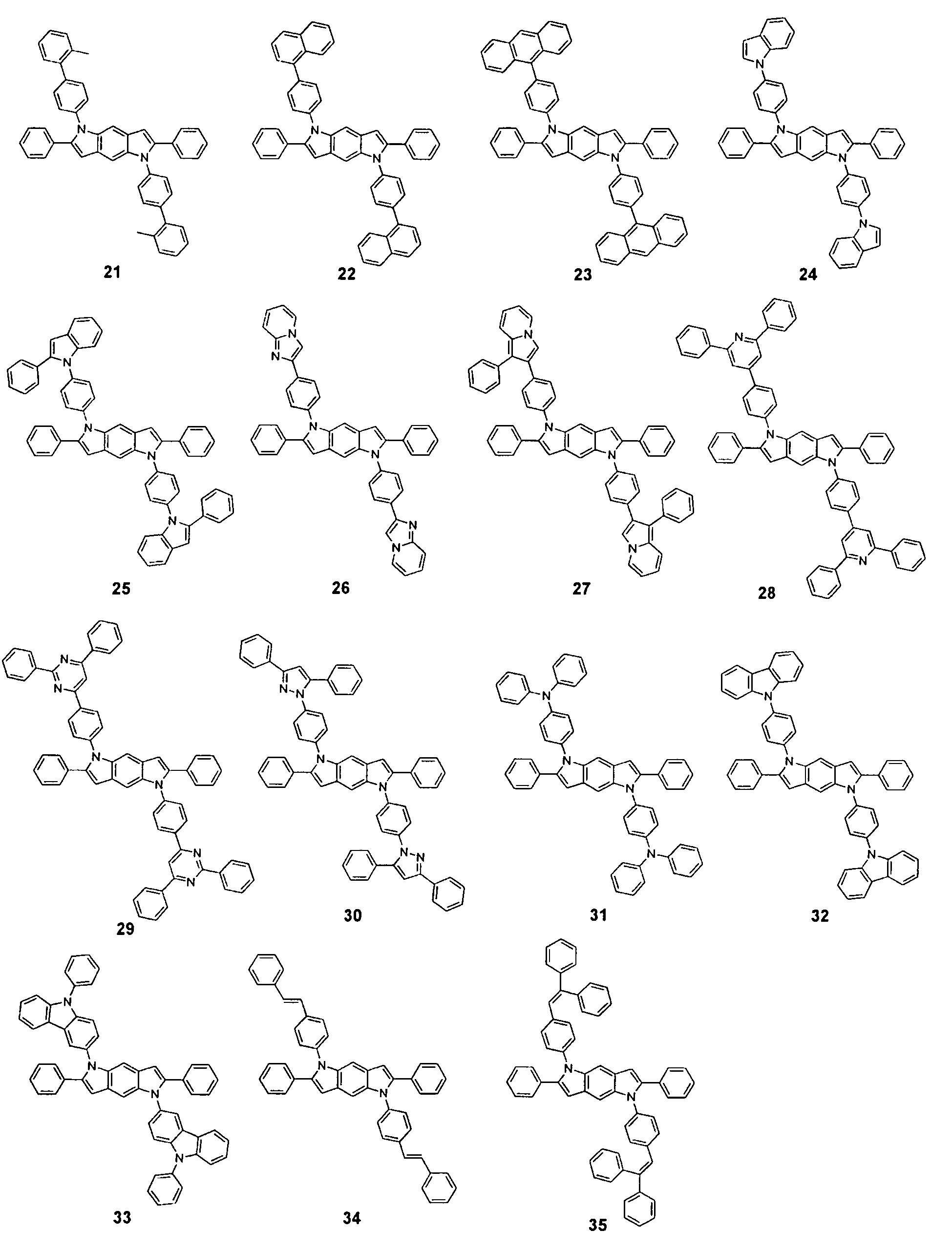
- heterocyclic compound represented by Formula 1 may be the compounds represented by Formulae 1 to 105, shown below, but are not limited thereto.
- Reaction Scheme 1 is for illustrative purposes only, and is not intended to limit the scope of the present invention.
- intermediate (b) 2,5-dimethyl-1,4-phenylenediamine (a) and compound (i) were reacted in the presence of a base, to prepare intermediate (b).
- L 1 of the compound (i) was a leaving group, for example, a bromo group, or an iodo group.
- the prepared intermediate (b) was reacted with compound (ii), to prepare intermediate (c).
- L 2 was a leaving group, selected from the group consisting of a chloro group, a bromo group, an anhydride, or a combination thereof.
- the prepared intermediate (c) was cyclization-reacted, at a high temperature and under a high pressure, to prepare compound (d).
- Ar 1 and Ar 2 are here each independently selected from the group consisting of a C6-C30 substituted or unsubstituted aryl group, a C6-C30 substituted or unsubstituted aryloxy group, a C4-C20 substituted or unsubstituted heterocyclic group, and a C6-C20 fused polycyclic group.
- An organic light emitting device includes a first electrode; a second electrode; and at least one organic layer interposed between the first electrode and the second electrode.
- the organic layer may include the heterocyclic compound represented by Formula 1, as described above.
- the organic light emitting device can have a variety of structures.
- the organic layer, including the heterocyclic compound of Formula 1 may include an emission layer, a hole injection layer, a hole transport layer, or a single layer that performs both hole injecting and transporting.
- the emission layer includes a blue light emission layer in some aspects.
- the organic light emitting device may have the structure shown in FIG. 1 , including an anode, a hole injection layer (HIL), a hole transport layer (HTL), an emission layer (EML), an electron transport layer (ETL), an electron injection layer (EIL), and a cathode, in a stacked structure.
- the organic light emitting device can include one or more intermediate layers.
- the compound of Formula 1 is particularly useful as a blue EML, due to its high color purity.
- An organic light emitting device including such an EML has excellent color purity and a large color gamut.
- the heterocyclic compound of Formula 1 has a high thermal resistance against heat generated in the organic layer, between the organic layers, and between the organic layer and the metal electrode, and is stable under such environments. Thus, the organic light emitting device has a high durability, and a long lifetime during storage and operation.
- a first electrode is formed by depositing, by sputtering for example, a high work-function material on the substrate.
- the substrate which can be any substrate that is used in conventional organic light emitting devices, and which has excellent mechanical strength, thermal stability, transparency, surface smoothness, is easily treated, and is waterproof.
- the substrate may be a glass substrate or a transparent plastic substrate, for example.
- the first electrode can be formed of ITO, IZO, SnO 2 , ZnO, or any highly conductive transparent material.
- the HIL can be formed on the first electrode, by for example, vacuum deposition, spin coating, casting, langmuir blodgett (LB), or the like.
- Any known HIL forming material can be used.
- vacuum deposition conditions may vary, according to the compound that is used to form the HIL, the desired structure, and thermal properties of the HIL. In general, however, the vacuum deposition may be performed at a deposition temperature of 50-500°C, under a pressure of 10 -8 -10 -3 torr, at a deposition speed of 0.01-100 ⁇ /sec, to a layer thickness of 10 ⁇ - 5 ⁇ m.
- coating conditions may vary, according to a compound that is used to form the HIL, and the desired structure and thermal properties of the HIL. In general, however, the coating speed may be in the range of about 2000 to 5000 rpm.
- the temperature for a heat treatment, which is performed to remove a solvent after coating, may be in the range of about 80 to 200°C.
- the HTL can also be formed using a known method, such as vacuum deposition, spin coating, casting, or LB.
- a known method such as vacuum deposition, spin coating, casting, or LB.
- the conditions for deposition and coating are similar to those for the formation of the HIL, although the conditions may vary, according to the material that is used to form the HTL.
- any known material that is commonly used to form an HTL can be used to form the HTL.
- the material include: carbazole derivatives, such as N-phenylcarbazole and polyvinylcarbazole; and conventional amine derivatives including a condensed aromatic ring, such as N,N'-bis(3-methylphenyl)-N,N'-diphenyl-[1,1-biphenyl-4,4'-diamine (TPD), and N,N'-di(naphthalene-1-yl)-N,N'-diphenyl benzydine ( ⁇ -NPD).
- carbazole derivatives such as N-phenylcarbazole and polyvinylcarbazole
- conventional amine derivatives including a condensed aromatic ring such as N,N'-bis(3-methylphenyl)-N,N'-diphenyl-[1,1-biphenyl-4,4'-diamine (TPD), and N,N'
- Red, green, and blue EMLs can be formed on the HIL and the HTL.
- Any material selected from known host materials and known dopant materials, can be used to form the EML.
- DCM1, DCM2, Eu(thenoyltrifluoroacetone)3 (Eu(TTA)3), and butyl-6-(1,1,7,7,-tetramethyljulolidyl-9-enyl)-4H-pyran (DCJTB) can be used to form the red EML.
- a dopant such as DCJTB can be deposited with Alq3, Alq3 and rubrene can be codeposited, and a dopant can be deposited thereon, or dopants such as BTPIr or RD 61 can be deposited with 4,4'-N-N'- dicarbazole-biphenyl (CBP), to form the red EML, but the present invention is not limited to the above-described examples.
- Coumarin 6, C545T, quinacridone, and Ir(ppy) 3 can be used to form the green EML.
- a dopant such as Ir(ppy) 3
- a dopant, such as a cuomarin-based material can be deposited with Alq3 as a host, to form the green EML, but the present invention is not limited to the above-described examples.
- the coumarin-based dopant may include C314S, C343S, C7, C7S, C6, C6S, C314T, and C545T.
- the heterocyclic compound of Formula 1 can only be used to form the blue EML region.
- the heterocyclic compound of Formula 1 can be used alone or in combination with compounds such as oxadiazole dimer dyes (Bis-DAPOXP), spiro compounds (Spiro-DPVBi, Spiro-6P), triarylamine compounds, bis(styryl) amine (DPVBi, DSA), CzTT, Anthracene, TPB, PPCP, DST, TPA, OXD-4, BBOT, AZM-Zn, and BH-013X (Idemitsu Corporation), which is an aromatic hydrocarbon compound containing a naphthalene moiety, to form the blue EML. It can also be used in combination with a dopant such as IDE 105 (Idemitsu Corporation), deposited on IDE 140 (Idemitsu Corporation), to form the blue EML.
- IDE 105 Idemitsu Corporation
- IDE 140 Idemitsu Corporation
- the thickness of the EML may be in the range of 200 to 500 ⁇ , and in some embodiments 300 to 400 ⁇ .
- the thickness of the EML of each of R, G, and B regions may be identical or different.
- the thickness of the EML is less than 200 ⁇ , the lifetime of the device may be decreased.
- the thickness of the EML is greater than 500 ⁇ , the driving voltage may be increased.
- the EML may be formed using a known method, such as vacuum deposition, spin coating, casting, and LB.
- a known method such as vacuum deposition, spin coating, casting, and LB.
- the conditions for deposition and coating are similar to those for the formation of the HIL, although the conditions may vary, according to the material that is used to form the EML.
- a hole blocking layer (HBL) (not shown) can optionally be formed on the EML, by vacuum depositing or spin coating a material that is used to form the HBL.
- the material should transport electrons, and have an ionization potential higher than the EML materials.
- the material may include bis(2-methyl-8-quinolato)-(p-phenylphenolato)-aluminum (Balq), bathocuproine (BCP), and tris(N-aryl benzimidazole) (TPBI), but are not limited thereto.
- the thickness of the HBL may be in the range of 30 to 60 ⁇ , and in some embodiments 40 to 50 ⁇ . When the thickness of the HBL is less than 30 ⁇ , a proper hole blocking capability may not be obtained. On the other hand, when the thickness of the HBL is greater than 60 ⁇ , the driving voltage of the device may be increased.
- the HBL can be formed using a known method, such as vacuum deposition, spin coating, casting, LB, or the like.
- a known method such as vacuum deposition, spin coating, casting, LB, or the like.
- conditions for deposition and coating are similar to those for formation of the HIL, although the conditions may vary, according to the material that is used to form the HBL.
- An ETL can be optionally formed by vacuum depositing or spin coating a material on the EML or the HBL.
- the material may be AIq3, but is not limited thereto.
- the thickness of the ETL may be in the range of 100 to 400 ⁇ , and in some embodiments 250 to 350 ⁇ . When the thickness of the ETL is less than 100 ⁇ , a proper charge balance may not be maintained, since electrons are transported too fast. On the other hand, when the thickness of the ETL is greater than 400 ⁇ , the driving voltage of the device may be increased.
- the ETL can be formed using a known method, such as vacuum deposition, spin coating, casting, LB, or the like.
- a known method such as vacuum deposition, spin coating, casting, LB, or the like.
- conditions for deposition and coating are similar to those for formation of the HIL, although the conditions may vary, according to the material that is used to form the ETL.
- the EIL may be formed by vacuum deposition or spin coating a material on the ETL.
- the material may be BaF 2 , LiF, NaCl, CsF, Li 2 O, BaO, Liq, or the like, but is not limited thereto.
- the thickness of the EIL may be in the range of 2 to 100 ⁇ , of in the range of 2 to 5 ⁇ . In some embodiments the thickness is in the range of 2 to 4 ⁇ . When the thickness of the EIL is less than 2 ⁇ , a proper electron injecting capability may not be obtained. On the other hand, when the thickness of the EIL is greater than 10 ⁇ , the driving voltage of the device may be increased.
- the EIL can be formed using a known method, such as vacuum deposition, spin coating, casting, LB, or the like.
- a known method such as vacuum deposition, spin coating, casting, LB, or the like.
- conditions for deposition and coating are similar to those for formation of the HIL, although the conditions may vary, according to the material that is used to form the EIL.
- a second electrode (cathode) is formed on the EIL, by deposition, thereby completing the manufacture of the organic light emitting device.
- the second electrode can be a transparent metal oxide with excellent conductivity, such as ITO, IZO, SnO 2 , and ZnO.
- Li, Mg, Al, Al-Li, Ca, Mg-In, Mg-Ag, and Ca-Al can be used to form a thin film on the second electrode.
- the second electrode can include a reflective electrode, and a semitransparent electrode, or a transparent electrode.
- the material used to form the second electrode is not limited to the above-described examples.
- a Corning 15 ⁇ /cm 2 (1200 ⁇ ) ITO glass substrate (used as an anode) was cut into pieces measuring 50 mm x 50 mm x 0.7 mm in size, then the pieces were cleaned by sonification in isopropyl alcohol and deionized water, for 5 minutes. Then the pieces were UV/ozone cleaned for 30 minutes.
- the glass substrate was installed in a vacuum deposition device.
- CBP represented by the formula below (as a known blue phosphorescent host) and Compound 2 were deposited at the same time, in a weight ratio of 98:2, on the HTL, to form an EML having a thickness of 300 ⁇ .
- LiF as a halogenated alkali metal was deposited on the ETL to a thickness of 10 ⁇ , to form an EIL, and Al was vacuum deposited to a thickness of 3000 ⁇ , to form a LiF/Al electrode (cathode), to prepare an organic light emitting device.
- FIG. 2 An emission spectrum of the prepared organic light emitting device was shown in FIG. 2 .
- the heterocyclic compound emits a blue color showing a main peak in the range of 400 to 450 nm in an emission spectrum.
- the organic light emitting device emitted a blue color with a high color purity, and the driving voltage of the organic light emitting device was 8.4 V, the brightness was 1,452 cd/m', the color coordinates were (0.149, 0.102), and the light emitting efficiency was 1.45 cd/A.
- An organic light emitting device was manufactured in the same manner as in Example 1, except that a compound represented by the formula below, was used instead of CBP as a host in the formation of the EML.
- the organic light emitting device emitted a blue color with high color purity, and the driving voltage of the organic light emitting device was 8.33 V, the brightness was 1,763cd/m 2 , the color coordinates were (0.147, 0.084), and the light emitting efficiency was 1.76 cd/A.
- An organic light emitting device was manufactured in the same manner as in Example 1 except that a compound represented by the formula below was used instead of CBP as a host in the formation of the EML.
- the organic light emitting device emitted a blue color with high color purity, and the driving voltage of the organic light emitting device was 8.25 V, the brightness was 1,526 cd/m 2 , the color coordinates were (0.147, 0.071), and the light emitting efficiency was 1.53 cd/A.
- An organic light emitting device was manufactured in the same manner as in Example 1, except that a compound represented by the formula below and Compound 12 were deposited at the same time, in a weight ratio of 98:2, to a thickness of 300 ⁇ , for the formation of the EML.
- the organic light emitting device emitted a blue color with high color purity, and the driving voltage of the organic light emitting device was 8.12 V, the brightness was 1,847 cd/m', the color coordinates were (0.147, 0.071), and the light emitting efficiency was 1.85 cd/A.
- Example Driving voltage V
- Current density mA/cm 2
- Brightness cd/m 2
- Light emitting efficiency cd/A
- Color coordinates x,y
- Example 1 8.40 100 1,452 1.45 (0.149, 0.102)
- Example 2 8.33 100 1,763 1.76 (0.147, 0.084)
- Example 3 8.25 100 1,526 1.53 (0.147, 0.071)
- Example 4 8.12 100 1,847 1.85 (0.147, 0.071)
- the CIE color coordinates, of the organic light emitting devices prepared according to Example 1-4 had high color purity. Especially, the CIE color coordinates of the organic light emitting device prepared according to Example 1 were nearly identical to color coordinates of the blue color specified by the NTSC. Therefore, the organic light emitting device according to aspects of the present invention, has excellent color reproduction range.
- an organic light emitting device emitting a blue color with a high color purity can be prepared. Since the heterocyclic compound emits a blue color with high electrical stability and a high color purity, an organic light emitting device having an excellent color gamut, particularly a large-scale bottom emission type organic light emitting device, can be prepared.
Landscapes
- Chemical & Material Sciences (AREA)
- Organic Chemistry (AREA)
- Engineering & Computer Science (AREA)
- Materials Engineering (AREA)
- Physics & Mathematics (AREA)
- Spectroscopy & Molecular Physics (AREA)
- Electroluminescent Light Sources (AREA)
- Nitrogen Condensed Heterocyclic Rings (AREA)
Abstract

Description
- Aspects of the present invention relate to a heterocyclic compound, and an organic light emitting device including the same, and more particularly, to a heterocyclic compound with high color purity and excellent electrical stability.
- Electroluminescent emitting devices, which are self-emitting devices, have wide viewing angles, excellent contrast, and quick response times, and thus, have drawn a large amount of public attention. Electroluminescent light emitting devices can be classified into two types, inorganic light emitting devices, which include an inorganic emission layer, and organic light emitting devices (OLED), which include an organic emission layer. An OLED has a higher brightness, a lower operating voltage, a quicker response time, and can realize more colors, as compared to an inorganic light emitting device.
- Typically, an OLED has an organic emission layer disposed between an anode and a cathode. An OLED can also have various other structures, such as a sequential stack of an anode, a hole transport layer, an organic emission layer, and a cathode, or sequential stack of an anode, a hole transport layer, an organic emission layer, an electron transport layer, and a cathode structure.
- The National Television System Committee (NTSC) has set a color reproduction standard, which is defined by color coordinates R(0.67, 0.33), G(0.21, 0.71), B(0.14, 0.08). The area defined by these color coordinates is 0.158. Accordingly, a blue light emitting material, with a color purity close to the color coordinates of (0.14, 0.08) of NTSC standard, is needed, in order to realize natural picture quality, by improving the color gamut of displays. Since liquid crystal displays (LCDs) use a color filter, in conjunction with a light emitting diode (LED) backlight, a blue color with high color purity can be simply realized. However, since organic light emitting devices are self-emitting devices, fluorescent or phosphorescent materials that emit a high purity blue color, are needed.
- However, only a sky blue color can be realized using known phosphorescent materials, and only a blue color with color coordinates of (0.15, 0.15) can be produced using current fluorescent materials. A top emission-type organic light emitting device has been developed, which is capable of realizing a high purity blue color, and a high efficiency, by using a sky blue fluorescent material, by incorporating a micro-cavity structure. However, in order to apply a micro-cavity structure to an organic light emitting device, optical length requirements need to be satisfied, and the thickness of the entire organic layer needs to be uniformly controlled. Thus, it is almost impossible to realize a large-scale organic light emitting device that can produce an acceptable color gamut. Therefore, in order to develop a large-scale organic light emitting device having a bottom emission structure, there is a need for a fluorescent light-emitting material that can emit a high color purity blue light.
- Aspects of the present invention provide a blue light emitting material, having a high electrical stability, and a high color purity.
- Aspects of the present invention also provide an organic light emitting device having excellent color reproduction, using the blue light-emitting material.
- According to an aspect of the present invention, there is provided a heterocyclic compound represented by Formula 1:

- X is selected from the group consisting of nitrogen, boron and phosphorous. Ar1, Ar2, Ar3, and Ar4 are each independently selected from the group consisting of a C6-C30 substituted or unsubstituted aryl group, a C6-C30 substituted or unsubstituted aryloxy group, a C4-C20 substituted or unsubstituted heterocyclic group, and a C6-C20 fused polycyclic group.
- According to another aspect of the present invention, there is provided an organic light emitting device including: a first electrode; a second electrode; and an organic layer interposed between the first electrode and the second electrode. The organic layer includes the heterocyclic compound.
- The heterocyclic compound, according to aspects of the present invention, can effectively emit a blue light that has high color purity, and has a high electrical stability. Thus, an organic light emitting device having characteristics, such as a high efficiency, a low driving voltage, a high brightness, and a long lifetime can be prepared using the heterocyclic compound.
- Additional aspects and/or advantages of the invention will be set forth in part in the description which follows and, in part, will be obvious from the description, or may be learned by practice of the invention.
- These and/or other aspects and advantages of the invention will become apparent, and more readily appreciated from, the following description of the exemplary embodiments, taken in conjunction with the accompanying drawings, of which:
-
FIG. 1 shows the structure of an organic light emitting device, according to an exemplary embodiment of the present invention; and -
FIG. 2 is a graph illustrating an emission spectrum of an organic light emitting device, according to an exemplary embodiment of the present invention. - Reference will now be made in detail to the exemplary embodiments of the present invention, examples of which are illustrated in the accompanying drawings, wherein like reference numerals refer to the like elements throughout. The exemplary embodiments are described below, in order to explain the aspects of the present invention, by referring to the figures.
- Aspects of the present invention provide an organic light emitting device that includes a heterocyclic compound, as a material used to form an organic layer. The heterocyclic compound has heterocyclic groups that are condensed into a single benzene ring. The heterocyclic compound is represented by the following Formula 1:

- X is selected from the group consisting of nitrogen, boron, and phosphorous, which are trivalent substituents. X may be nitrogen for ease of preparation and color purity. Ar1, Ar2, Ar3, and Ar4 are each independently selected from a C6-C30 substituted or unsubstituted aryl group, a C6-C30 substituted or unsubstituted aryloxy group, a C4-C20 substituted or unsubstituted heterocyclic group, and a C6-C20 condensed polycyclic group.
- An unsubstituted aryl group, applied to the compound of Formula 1, may be used alone or in combination. The aryl group indicates an aromatic carbocyclic system having 6-30 carbon atoms, and one or more rings. The rings may be bonded together in a pendent manner, or may be fused. Examples of the unsubstituted aryl group include a phenyl group, a naphthyl group, a biphenyl group, a terphenyl group, and a pentaphenyl group. At least one of the hydrogen atoms of the aryl group may be substituted with a C1-C5 alkyl group, a C1-C5 alkoxy group, a C6-C14 aryl group, a C6-C20 aryloxy group, a halogen atom, an amino group, or a cyano group. More particular examples of the aryl group are a phenyl group, an ethylphenyl group, a propylphenyl group, a butylphenyl group, a tert-butylnyl group, an o-, m- and p-fluorophenyl group, a difluorophenyl group, a trifluorophenyl group, a cyanophenyl group, a methoxyphenyl group, a phenoxyphenyl group, an o-, m-, and p-tolyl group, a (α,α-dimethylbenzene)phenyl group, a (N,N'-dimethyl)aminophenyl group, a (N,N'-diphenyl)aminophenyl group, a biphenyl group, a terphenyl group, a 3,5-diphenylphenyl group, a quarterphenyl group, and a pentaphenyl group, but are not limited thereto.
- Examples of the unsubstituted heteroaryl group, applied to the compound of Formula 1, are a furanyl group, a pyridinyl group, and a thiophenyl group. At least one of the hydrogen atoms of the heteroaryl group may be substituted with a C1-C5 alkyl group, or the like.
- Examples of the unsubstituted fused polycyclic group, applied to the compound of Formula 1, are a pentalenyl group, a naphthyl group, an azulenyl group, a heptalenyl group, an acenaphtyl group, an anthryl group, a phenanthryl group, a quinolyl group, an anthraquinolyl group, a fluorenyl group, and a carbazolyl group. At least one of the hydrogen atoms of the fused polycyclic group may be substituted with a C1-C5 alkyl group, a C1-C5 alkoxy group, a C6-C14 aryl group, a C6-C20 aryloxy group, a halogen atom, an amino group, or a cyano group. More particular examples of the unsubstituted fused polycyclic group are a pentalenyl group, a naphthyl group, a methylnaphthyl group, an anthracenyl group, an azulenyl group, a heptalenyl group, an acenaphthylenyl group, a fluorenyl group, a 9,9-dimethylfluorenyl group, a 9,9-diphenylfluorenyl group, an anthraquinolyl group, a penanthryl group, a triphenylene group, a carbazolyl group, and a 9-phenylcarbazolyl group, but are not limited thereto.
- Examples of the unsubstituted aryloxy group, applied to the compound of Formula 1, are a phenyloxy group, a naphthyloxy group, an anthryloxy group, and a penanthryloxy group. At least one of the hydrogen atoms of the aryloxy group may be substituted with a C1-C5 alkyl group, a C1-C5 alkoxy group, a C6-C14 aryl group, a C6-C20 aryloxy group, a halogen atom, an amino group, or a cyano group.
- Ar1, Ar2, Ar3, and Ar4 may be each independently selected from a phenyl group, a naphthyl group, a biphenyl group, a terphenyl group, a fluorenyl group, a carbazolyl group, a pyridyl group, a quinolyl group and derivatives thereof (at least one of the hydrogen atoms of which may be substituted with a C1-C5 short-chain alkyl group, a C1-C5 short-chain alkoxy group, a cyano group, an amine group, a phenoxy group, a phenyl group, or a halogen group). More specifically, Ar1, Ar2, Ar3, and Ar4 may each be a phenyl group, a phenyl group substituted with a C1-C5 alkyl group, a phenyl group substituted with a C1-C5 alkoxy group, a cyanophenyl group, a halophenyl group, a phenoxyphenyl group, a phenyl group substituted with a fluorenyl group, a naphthyl group, a naphthyl group substituted with a C1-C5 alkyl group, a naphthyl group substituted with a C1-C5 alkoxy group, a cyanonaphthyl group, a halonaphthyl group, a biphenyl group, a biphenyl group substituted with a C1-C5 alkyl group, a biphenyl group substituted with a C1-C5 alkoxy group, a diphenylphenyl group, a terphenyl group, a pyridyl group, a fluorenyl group, a fluorenyl group substituted with a C1-C5 alkyl group, a diphenyl fluorenyl group, or a quinolyl group. More particularly, Ar1, Ar2, Ar3, and Ar4 may be a phenyl group, an ethylphenyl group, a propylphenyl group, a butylphenyl group, a tert-butylphenyl group, an o-, m- and p-fluorophenyl group, a difluorophenyl group, a trifluorophenyl group, a cyanophenyl group, a methoxyphenyl group, a phenoxyphenyl group, an o-, m-, and p-tolyl group, a (α,α-dimethylbenzene)phenyl group, a (N,N'-dimethyl)aminophenyl group, a (N,N'-diphenyl)aminophenyl group, a biphenyl group, a terphenyl group, a 3,5-diphenylphenyl group, a quarterphenyl group, a pentaphenyl group, an anthryl group, fluorenyl group, a 9,9-dimethylfluorenyl group, a 9,9-diphenylfluorenyl group, a carbazolyl group, or a 9-phenylcarbazolyl group.
- In the compound of Formula1, Ar1 Ar3 may be identical, and Ar2 and Ar4 may be identical, for ease of preparation. The heterocyclic compound may be represented by Formula 2 below:

- X, Ar1, and Ar2 are the same as described above.
- Since the heterocyclic compound of Formula 1 includes a strong 3-ring structure, the glass transition temperature (Tg), and/or the melting point of the compound, is increased. Accordingly, the organic light-emitting device has an increased thermal resistance against heat generated in the organic layer, between the organic layers, and between the organic layer and the metal electrode. The organic light emitting device is stable in hot environments. Thus, the organic light emitting device has a high durability during storage and operation. The compound represented by Formula 1 can be a hole injecting material, a hole transporting material, and/or an emitting material.
- Examples of the heterocyclic compound represented by Formula 1, may be the compounds represented by Formulae 1 to 105, shown below, but are not limited thereto.


- Hereinafter, a method of preparing a heterocyclic compound, according to aspects of the present invention, will be described in detail with reference to Reaction Scheme 1, below. However, Reaction Scheme 1 is for illustrative purposes only, and is not intended to limit the scope of the present invention.

- First, 2,5-dimethyl-1,4-phenylenediamine (a) and compound (i) were reacted in the presence of a base, to prepare intermediate (b). L1 of the compound (i) was a leaving group, for example, a bromo group, or an iodo group. The prepared intermediate (b) was reacted with compound (ii), to prepare intermediate (c). In compound (ii), L2 was a leaving group, selected from the group consisting of a chloro group, a bromo group, an anhydride, or a combination thereof. The prepared intermediate (c) was cyclization-reacted, at a high temperature and under a high pressure, to prepare compound (d).
- Ar1 and Ar2 are here each independently selected from the group consisting of a C6-C30 substituted or unsubstituted aryl group, a C6-C30 substituted or unsubstituted aryloxy group, a C4-C20 substituted or unsubstituted heterocyclic group, and a C6-C20 fused polycyclic group.
- An organic light emitting device, according to aspects of the present invention, includes a first electrode; a second electrode; and at least one organic layer interposed between the first electrode and the second electrode. The organic layer may include the heterocyclic compound represented by Formula 1, as described above.
- The organic light emitting device can have a variety of structures. The organic layer, including the heterocyclic compound of Formula 1, may include an emission layer, a hole injection layer, a hole transport layer, or a single layer that performs both hole injecting and transporting. The emission layer includes a blue light emission layer in some aspects.
- The organic light emitting device may have the structure shown in
FIG. 1 , including an anode, a hole injection layer (HIL), a hole transport layer (HTL), an emission layer (EML), an electron transport layer (ETL), an electron injection layer (EIL), and a cathode, in a stacked structure. The organic light emitting device can include one or more intermediate layers. - The compound of Formula 1 is particularly useful as a blue EML, due to its high color purity. An organic light emitting device including such an EML has excellent color purity and a large color gamut. The heterocyclic compound of Formula 1 has a high thermal resistance against heat generated in the organic layer, between the organic layers, and between the organic layer and the metal electrode, and is stable under such environments. Thus, the organic light emitting device has a high durability, and a long lifetime during storage and operation.
- Hereinafter, a method of manufacturing an organic light emitting device, according to an exemplary embodiment of the present invention, will be described with reference to the organic light emitting device illustrated in
FIG. 1 . First, a first electrode (anode) is formed by depositing, by sputtering for example, a high work-function material on the substrate. The substrate, which can be any substrate that is used in conventional organic light emitting devices, and which has excellent mechanical strength, thermal stability, transparency, surface smoothness, is easily treated, and is waterproof. The substrate may be a glass substrate or a transparent plastic substrate, for example. The first electrode can be formed of ITO, IZO, SnO2, ZnO, or any highly conductive transparent material. - Then, the HIL can be formed on the first electrode, by for example, vacuum deposition, spin coating, casting, langmuir blodgett (LB), or the like. Any known HIL forming material can be used. For example, 1,3,5-tricarbazolylbenzene, 4,4'-biscarbazolylbiphenyl, polyvinyl carbazole, m-biscarbazolylphenyl, 4,4'-biscarbazolyl-2,2'-dimethylbiphenyl, 4,4',4"-tri(N-carbazolyl)triphenylamine, 1,3,5-tri(2-carbazolylphenyl)benzene, 1,3,5-tris(2-carbazolyl-5-methoxyphenyl)benzene, bis(4-carbazolylphenyl)silane, N,N'-bis(3-methylphenyl)-N,N'-diphenyl-[1,1-biphenyl]-4,4'diamine (TPD), N,N'-di(naphthalene-1-yl)-N,N'-diphenyl benzydine (α-NPD), N,N'-diphenyl-N,N'-bis(1-naphthyl)-(1,1'-biphenyl)-4,4'-diamine (NPB), poly(9,9-dioctylfluorene-co-N-(4-butylphenyl)diphenylamine) (TFB), and poly(9,9-dioctylfluorene-co-bis-N,N-phenyl-1,4-phenylenediamine (PFB) can be used.
- When the HIL is formed by vacuum deposition, vacuum deposition conditions may vary, according to the compound that is used to form the HIL, the desired structure, and thermal properties of the HIL. In general, however, the vacuum deposition may be performed at a deposition temperature of 50-500°C, under a pressure of 10-8 -10-3torr, at a deposition speed of 0.01-100 Å /sec, to a layer thickness of 10 Å - 5 µm.
- When the HIL is formed by spin coating, coating conditions may vary, according to a compound that is used to form the HIL, and the desired structure and thermal properties of the HIL. In general, however, the coating speed may be in the range of about 2000 to 5000 rpm. The temperature for a heat treatment, which is performed to remove a solvent after coating, may be in the range of about 80 to 200°C.
- The HTL can also be formed using a known method, such as vacuum deposition, spin coating, casting, or LB. When the HTL is formed by vacuum deposition or spin coating, the conditions for deposition and coating are similar to those for the formation of the HIL, although the conditions may vary, according to the material that is used to form the HTL.
- Any known material that is commonly used to form an HTL can be used to form the HTL. Examples of the material include: carbazole derivatives, such as N-phenylcarbazole and polyvinylcarbazole; and conventional amine derivatives including a condensed aromatic ring, such as N,N'-bis(3-methylphenyl)-N,N'-diphenyl-[1,1-biphenyl-4,4'-diamine (TPD), and N,N'-di(naphthalene-1-yl)-N,N'-diphenyl benzydine (α-NPD).
- Red, green, and blue EMLs (EML regions) can be formed on the HIL and the HTL. Any material, selected from known host materials and known dopant materials, can be used to form the EML. For example, DCM1, DCM2, Eu(thenoyltrifluoroacetone)3 (Eu(TTA)3), and butyl-6-(1,1,7,7,-tetramethyljulolidyl-9-enyl)-4H-pyran (DCJTB) can be used to form the red EML. Alternatively, a dopant such as DCJTB can be deposited with Alq3, Alq3 and rubrene can be codeposited, and a dopant can be deposited thereon, or dopants such as BTPIr or RD 61 can be deposited with 4,4'-N-N'- dicarbazole-biphenyl (CBP), to form the red EML, but the present invention is not limited to the above-described examples.
- For example, Coumarin 6, C545T, quinacridone, and Ir(ppy)3 can be used to form the green EML. Alternatively, a dopant, such as Ir(ppy)3, can be deposited with CBP, or a dopant, such as a cuomarin-based material, can be deposited with Alq3 as a host, to form the green EML, but the present invention is not limited to the above-described examples. Examples of the coumarin-based dopant may include C314S, C343S, C7, C7S, C6, C6S, C314T, and C545T.
- The heterocyclic compound of Formula 1 can only be used to form the blue EML region. The heterocyclic compound of Formula 1 can be used alone or in combination with compounds such as oxadiazole dimer dyes (Bis-DAPOXP), spiro compounds (Spiro-DPVBi, Spiro-6P), triarylamine compounds, bis(styryl) amine (DPVBi, DSA), CzTT, Anthracene, TPB, PPCP, DST, TPA, OXD-4, BBOT, AZM-Zn, and BH-013X (Idemitsu Corporation), which is an aromatic hydrocarbon compound containing a naphthalene moiety, to form the blue EML. It can also be used in combination with a dopant such as IDE 105 (Idemitsu Corporation), deposited on IDE 140 (Idemitsu Corporation), to form the blue EML.
- The thickness of the EML may be in the range of 200 to 500 Å, and in some embodiments 300 to 400 Å. The thickness of the EML of each of R, G, and B regions may be identical or different. When the thickness of the EML is less than 200 Å, the lifetime of the device may be decreased. On the other hand, when the thickness of the EML is greater than 500 Å, the driving voltage may be increased.
- The EML may be formed using a known method, such as vacuum deposition, spin coating, casting, and LB. When the EML is formed by vacuum deposition or spin coating, the conditions for deposition and coating are similar to those for the formation of the HIL, although the conditions may vary, according to the material that is used to form the EML.
- A hole blocking layer (HBL) (not shown) can optionally be formed on the EML, by vacuum depositing or spin coating a material that is used to form the HBL. The material should transport electrons, and have an ionization potential higher than the EML materials. Examples of the material may include bis(2-methyl-8-quinolato)-(p-phenylphenolato)-aluminum (Balq), bathocuproine (BCP), and tris(N-aryl benzimidazole) (TPBI), but are not limited thereto.
- The thickness of the HBL may be in the range of 30 to 60 Å, and in some embodiments 40 to 50 Å. When the thickness of the HBL is less than 30 Å, a proper hole blocking capability may not be obtained. On the other hand, when the thickness of the HBL is greater than 60 Å, the driving voltage of the device may be increased.
- The HBL can be formed using a known method, such as vacuum deposition, spin coating, casting, LB, or the like. When the HBL is formed by vacuum deposition or spin coating, conditions for deposition and coating are similar to those for formation of the HIL, although the conditions may vary, according to the material that is used to form the HBL.
- An ETL can be optionally formed by vacuum depositing or spin coating a material on the EML or the HBL. The material may be AIq3, but is not limited thereto.
- The thickness of the ETL may be in the range of 100 to 400 Å, and in some embodiments 250 to 350 Å. When the thickness of the ETL is less than 100 Å, a proper charge balance may not be maintained, since electrons are transported too fast. On the other hand, when the thickness of the ETL is greater than 400 Å, the driving voltage of the device may be increased.
- The ETL can be formed using a known method, such as vacuum deposition, spin coating, casting, LB, or the like. When the ETL is formed by vacuum deposition or spin coating, conditions for deposition and coating are similar to those for formation of the HIL, although the conditions may vary, according to the material that is used to form the ETL.
- The EIL may be formed by vacuum deposition or spin coating a material on the ETL. The material may be BaF2, LiF, NaCl, CsF, Li2O, BaO, Liq, or the like, but is not limited thereto.
- The thickness of the EIL may be in the range of 2 to 100 Å, of in the range of 2 to 5 Å. In some embodiments the thickness is in the range of 2 to 4 Å. When the thickness of the EIL is less than 2 Å, a proper electron injecting capability may not be obtained. On the other hand, when the thickness of the EIL is greater than 10 Å, the driving voltage of the device may be increased.
- The EIL can be formed using a known method, such as vacuum deposition, spin coating, casting, LB, or the like. When the EIL is formed by vacuum deposition or spin coating, conditions for deposition and coating are similar to those for formation of the HIL, although the conditions may vary, according to the material that is used to form the EIL.
- Finally, a second electrode (cathode) is formed on the EIL, by deposition, thereby completing the manufacture of the organic light emitting device. The second electrode can be a transparent metal oxide with excellent conductivity, such as ITO, IZO, SnO2, and ZnO. Optionally, Li, Mg, Al, Al-Li, Ca, Mg-In, Mg-Ag, and Ca-Al can be used to form a thin film on the second electrode. Thus, the second electrode can include a reflective electrode, and a semitransparent electrode, or a transparent electrode. The material used to form the second electrode is not limited to the above-described examples.
- Hereinafter, aspects of the present invention will be described with reference to the following Synthesis Examples of heterocyclic compounds represented by Formula 1, and Preparation Examples of an organic light emitting device. However, the Examples are not intended to limit the scope of the present invention.
- Compound 2 was synthesized through Reaction Scheme 2 below.

- 1.36 g (10.0 mmol) of 2,5-dimethyl-1,4-phenylenediamine and 4.10 g (24.0 mmol) of 4-bromotoluene were dissolved in 50 Mℓ of toluene. 2.88 g (30.0 mmol) of sodium t-butoxide, 0.388 g (0.40 mmol) of Pd(dba)2 and 0.08 g (0.40 mmol) of tri-t-butylphosphine((t-Bu)3P) were added to the solution, and the mixture was stirred at 80 °C, for 5 hours. The resultant mixture was cooled to room temperature, and then 50 Mℓ of water was added thereto. The resultant mixture was subjected to extraction three times, using 20 Mℓ of ethyl ether. A collected organic layer was dried using magnesium sulfate, and the residue (prepared by removing the solvent) was separated and purified using a silica gel column chromatography, to obtain 2.15 g of Intermediate A (Yield: 68 %).
- 1H NMR (CDCl3, 400MHz) δ (ppm) 7.24-7.33 (m, 4H), 7.09 (s, 2H), 6.85-6.78 (m, 4H), 5.25 (bs, 2H), 2.32 (s, 6H), 2.17 (s, 6H); 13C NMR (CDCl3, 100MHz) δ (ppm) 145.8, 133.2, 128.5, 127.8, 123.8, 122.5, 116.8, 17.6, 15.7.
- 3.16 g (10.0 mmol) of Intermediate A was dissolved in 50 Mℓ of dichloromethane, and 4.0 Mℓ of triethylamine was the added thereto. The mixture was cooled in an ice bath, and 4.21 g (30.0 mmol) of benzoyl chloride was dropped thereto. The resultant was stirred at 30 °C, for 1 hour, and 50 Mℓ of water was added thereto. Then, the resultant was subject to extraction three times, using 50 Mℓ of ethyl ether. A collected organic layer was dried using magnesium sulfate, and the residue prepared by removing the solvent was recrystallized in DMF. The resultant was filtered, while washing with acetone, to obtain 2.99 g of white solid Intermediate B (Yield: 57 %).
- 1H NMR (CDCl3, 400MHz) δ (ppm) 8.11-8.09 (d, 2H), 7.48-7.46 (m, 4H), 7.27-6.89 (m, 14 H), 2.17 (s, 6H), 2.10 (s, 6H); 13C NMR (CDCl3, 100MHz) δ (ppm) 170.4, 143.3, 135.5, 133.7, 130.0, 129.3, 128.9, 128.8, 127.8, 125.5, 120.9, 118.2, 18.0, 17.3.
- A mixture, prepared by sufficiently pulverizing and stirring 5.24 g (10 mmol) of Intermediate B and 12.2 g (100 mmol) of potassium t-butoxide, was added to an autoclave, and reacted at 340-350 °C, at 5 MPa, for 2 hours. When the reaction was completed, the resultant tar was cooled to room temperature. The tar was pulverized, neutralized, filtered using distilled water, and dried. The residue was purified in a soxhlet device, using acetone, for 2 days, to obtain 0.97 g of yellow Compound 2 (Yield: 20%).
- 1H NMR (CDCl3, 400MHz) δ (ppm) 7.46 (s, 2H), 7.31-7.18 (m, 18H), 6.74 (s, 2H), 2.41 (s, 3H); 13C NMR (CDCl3, 100MHz) δ (ppm) 141.4, 137.3, 136.9, 136.6, 133.1, 129.9, 128.8, 128.1, 128.0, 127.0, 126.4, 103.3, 99.8, 22.1.
- Compound 12 was synthesized through Reaction Scheme 3 below.

- 1.36 g (10.0 mmol) of 2,5-dimethyl-1,4-phenylenediamine and 5.13 g (22.0 mmol) of 4-bromobiphenyl was dissolved in 50 Mℓ of toluene. 2.88 g (30.0 mmol) of sodium t-butoxide, 0.388 g (0.40 mmol) of Pd(dba)2, and 0.08 g (0.40 mmol) of tri-t-butylphosphine((t-Bu)3P) were added to the solution, and the mixture was stirred at 80 °C, for 5 hours. The resultant mixture was cooled to room temperature, and then 50 Mℓ of water was added thereto, and the resultant was subjected to extraction three times, using 20 Mℓ of ethyl ether. A collected organic layer was dried using magnesium sulfate, and the residue prepared by removing the solvent was separated and purified, using a silica gel column chromatography, to obtain 3.13 g of Intermediate C (Yield: 71 %).
- 1H NMR (CDCl3, 400MHz) δ (ppm) 7.24-7.04 (m, 14H), 6.75-6.58 (m, 4H), 5.12 (bs, 2H), 2.17 (s, 6H); 13C NMR (CDCl3, 100MHz) δ (ppm) 145.8, 133.2, 131.5, 129.7, 128.5, 127.8, 124.3, 123.8, 122.5, 119.5, 116.8, 17.6.
- 4.40 g (10.0 mmol) of Intermediate C was dissolved in 50 Mℓ of dichloromethane, and 4.0 Mℓ of triethylamine was added thereto. The mixture was cooled in an ice bath, and 4.21 g (30.0 mmol) of benzoyl chloride was dropped thereto. The resultant was stirred at 30 °C, for 1 hour, and 50 Mℓ of water was added thereto. Then, the resultant was subject to extraction three times, using 50 Mℓ of ethyl ether. A collected organic layer was dried using magnesium sulfate, and the residue prepared by removing the solvent was recrystallized in DMF. The resultant was filtered while washing with acetone, to obtain 4.34 g of white solid Intermediate D (Yield: 67 %).
- 1 H NMR (CDCl3, 400MHz) δ (ppm) 8.21-8.11 (d, 2H), 7.59-6.78 (m, 28H), 2.17 (s, 6H); 13C NMR (CDCl3, 100MHz) δ (ppm) 170.0, 141.3, 135.6, 135.1, 132.7, 131.3, 129.3, 129.1, 128.9, 128.8, 127.8, 125.5, 120.9, 119.8, 118.2, 18.0.
- A mixture prepared by sufficiently pulverizing and stirring 6.48 g (10 mmol) of Intermediate D, and 12.2 g (100 mmol) of potassium t-butoxide was added to an autoclave, and reacted at 340-350 °C, at 5 MPa, for 2 hours. When the reaction was completed, the resultant tar was cooled to room temperature. The tar was pulverized, neutralized, filtered while washing distilled water, and dried. The residue was purified in a soxhlet device using acetone, for 2 days, to obtain 0.86 g of light yellow Compound 12 (Yield: 14 %).
- 1H NMR (CD2Cl2, 400MHz) δ (ppm) 7.72-7.67 (m, 8H), 7.57-7.37 (m, 14H), 7.32-7.25 (m, 8H) 6.82 (s, 2H); 13C NMR (CD2Cl2, 100MHz) δ (ppm) 141.2, 135.1, 134.9, 134.6, 133.1, 129.4, 128.4, 128.0, 127.4, 127.0, 126.3, 126.0, 125.1, 124.3, 121.2, 103.3, 101.8.
- Compound 71 was synthesized through Reaction Scheme 4 below.

- 1.36 g (10.0 mmol) of 2,5-dimethyl-1,4-phenylenediamine and 3.77 g (24.0 mmol) of 4-bromobenzene were dissolved in 50 Mℓ of toluene. 2.88 g (30.0 mmol) of sodium t-butoxide, 0.388 g (0.40 mmol) of Pd(dba)2, and 0.08 g (0.40 mmol) of tri-t-butylphosphine((t-Bu)3P) were added to the solution, and the mixture was stirred at 80 °C, for 5 hours. The resultant mixture was cooled to room temperature, and then 50 Mℓ of water was added thereto, and the resultant was subjected to extraction three times, using 20 Mℓ of ethyl ether. A collected organic layer was dried using magnesium sulfate, and the residue prepared by removing the solvent was separated and purified, using a silica gel column chromatography, to obtain 1.78 g of Intermediate E (Yield: 62 %).
- 1H NMR (CDCl3, 400MHz) δ (ppm) 7.28-6.89 (m, 12H), 5.43 (s, 2H), 2.15 (s, 3H); 13C NMR (CDCl3, 100MHz) δ (ppm) 147.5, 139.2, 134.9, 129.3, 121.0, 117.5, 18.2.
- 4.40 g (10.0 mmol) of Intermediate E was dissolved in 50 Mℓ of dichloromethane, and 4.0 Mℓ of triethylamine was added thereto. The mixture was cooled in an ice bath, and 6.50 g (30.0 mmol) 4-biphenylcarbonyl chloride was dropped thereto. The resultant was stirred at 30 °C, for 1 hour, and 50 Mℓ of water was added thereto. Then, the resultant was subject to extraction three times, using 50 Mℓ of ethyl ether. A collected organic layer was dried using magnesium sulfate, and the residue prepared by removing the solvent was recrystallized in DMF. The resultant was filtered while washing with acetone, to obtain 4.21 g of light yellow solid Intermediate F (Yield: 65 %).
- 1H NMR (CDCl3, 400MHz) δ (ppm) 7.44-6.89 (m, 30H), 2.14 (s, 6H); 13C NMR (CDCl3, 100MHz) δ (ppm) 160.9, 143.2, 142.3, 141.2, 136.7, 135.8, 134.9, 134.2, 130.3, 129.4, 128.9, 127.8, 126.8, 126.4, 125.8, 124.5, 17.8.
- A mixture prepared by sufficiently pulverizing and stirring 6.48 g (10 mmol) of Intermediate F and 12.2 g (100 mmol) of potassium t-butoxide was added to an autoclave, and reacted at 340-350 °C, at 5 MPa, for 2 hours. When the reaction was completed, the resultant tar was cooled to room temperature. The tar was pulverized, neutralized, filtered while washing with distilled water, and dried. The residue was purified in a soxhlet device using acetone, for 2 days, to obtain 1.12 g of light yellow Compound 11 (Yield: 18 %).
- 1H NMR (CD2Cl2, 400MHz) δ (ppm) 7.98-7.65 (m, 8H), 7.48-7.32 (m, 14H), 7.22-7.12 (m, 8H) 6.80 (s, 2H); 13C NMR (CD2Cl2, 100MHz) δ (ppm) 145.2, 136.1, 134.5, 134.1, 133.2, 128.4, 127.4, 126.0, 125.8, 125.0, 123.2, 122.3, 121.1, 121.0, 119.2, 102.3, 101.9.
- A Corning 15 Ω/cm2 (1200Å) ITO glass substrate (used as an anode) was cut into pieces measuring 50 mm x 50 mm x 0.7 mm in size, then the pieces were cleaned by sonification in isopropyl alcohol and deionized water, for 5 minutes. Then the pieces were UV/ozone cleaned for 30 minutes. The glass substrate was installed in a vacuum deposition device.
- 4,4',4"-tris[2-naphthyl(phenyl)aminotriphenylamine (2-TNATA), represented by the formula, below was vacuum deposited to a thickness of 600 Å on the substrate, to form a HIL. Then, 4,4'-bis[N-(1-naphthyl)-N-phenylaminobiphenyl (NPB), represented by the formula below, as a hole transporting compound was vacuum deposited to a thickness of 300°C, on the HIL, to form a HTL.

- CBP represented by the formula below (as a known blue phosphorescent host) and Compound 2 were deposited at the same time, in a weight ratio of 98:2, on the HTL, to form an EML having a thickness of 300 Å.

- Then, Alq3 was deposited on the EML to a thickness of 300 Å, to form an ETL. LiF as a halogenated alkali metal was deposited on the ETL to a thickness of 10 Å, to form an EIL, and Al was vacuum deposited to a thickness of 3000 Å, to form a LiF/Al electrode (cathode), to prepare an organic light emitting device.
- An emission spectrum of the prepared organic light emitting device was shown in
FIG. 2 . Referring toFIG. 2 , the heterocyclic compound emits a blue color showing a main peak in the range of 400 to 450 nm in an emission spectrum. - At a current density of 100 mA/cm2, the organic light emitting device emitted a blue color with a high color purity, and the driving voltage of the organic light emitting device was 8.4 V, the brightness was 1,452 cd/m', the color coordinates were (0.149, 0.102), and the light emitting efficiency was 1.45 cd/A.
- An organic light emitting device was manufactured in the same manner as in Example 1, except that a compound represented by the formula below, was used instead of CBP as a host in the formation of the EML.

- At a current density of 100 mA/cm2, the organic light emitting device emitted a blue color with high color purity, and the driving voltage of the organic light emitting device was 8.33 V, the brightness was 1,763cd/m2, the color coordinates were (0.147, 0.084), and the light emitting efficiency was 1.76 cd/A.
- An organic light emitting device was manufactured in the same manner as in Example 1 except that a compound represented by the formula below was used instead of CBP as a host in the formation of the EML.

- At a current density of 100 mA/cm2, the organic light emitting device emitted a blue color with high color purity, and the driving voltage of the organic light emitting device was 8.25 V, the brightness was 1,526 cd/m2, the color coordinates were (0.147, 0.071), and the light emitting efficiency was 1.53 cd/A.
- An organic light emitting device was manufactured in the same manner as in Example 1, except that a compound represented by the formula below and Compound 12 were deposited at the same time, in a weight ratio of 98:2, to a thickness of 300 Å, for the formation of the EML.

- At a current density of 100 mA/cm2, the organic light emitting device emitted a blue color with high color purity, and the driving voltage of the organic light emitting device was 8.12 V, the brightness was 1,847 cd/m', the color coordinates were (0.147, 0.071), and the light emitting efficiency was 1.85 cd/A.
- The results of the organic light emitting devices according to Examples 1 to 4 were shown in Table 1.
Table 1 Example Driving voltage (V) Current density (mA/cm2) Brightness (cd/m2) Light emitting efficiency (cd/A) Color coordinates (x,y) Example 1 8.40 100 1,452 1.45 (0.149, 0.102) Example 2 8.33 100 1,763 1.76 (0.147, 0.084) Example 3 8.25 100 1,526 1.53 (0.147, 0.071) Example 4 8.12 100 1,847 1.85 (0.147, 0.071) - As shown in Table 1, the CIE color coordinates, of the organic light emitting devices prepared according to Example 1-4 had high color purity. Especially, the CIE color coordinates of the organic light emitting device prepared according to Example 1 were nearly identical to color coordinates of the blue color specified by the NTSC. Therefore, the organic light emitting device according to aspects of the present invention, has excellent color reproduction range.
- As described above, as a result of using the compound represented by Formula 1 to form an emission layer, an organic light emitting device emitting a blue color with a high color purity, can be prepared. Since the heterocyclic compound emits a blue color with high electrical stability and a high color purity, an organic light emitting device having an excellent color gamut, particularly a large-scale bottom emission type organic light emitting device, can be prepared.
Claims (11)
- A heterocyclic compound represented by Formula 1:

the Ar1, Ar2, Ar3, and Ar4 are each independently selected from the group consisting of a C6-C30 substituted or unsubstituted aryl group, a C6-C30 substituted or unsubstituted aryloxy group, a C4-C20 substituted or unsubstituted heterocyclic group, and a C6-C20 fused polycyclic group. - The heterocyclic compound of claim 1, wherein:the Ar1, Ar2, Ar3, and Ar4 are each independently selected from the group consisting of a phenyl group, a naphthyl group, a biphenyl group, a terphenyl group, a fluorenyl group, a carbazolyl group, a pyridyl group, a quinolyl group, and derivatives thereof, in which at least one of the hydrogen atoms is optionally substituted with a C1-C5 short-chain alkyl group, a C1-C5 short-chain alkoxy group, a cyano group, an amine group, a phenoxy group, a phenyl group, or a halogen group.
- The heterocyclic compound of claim 1 or 2, wherein the Ar1 and Ar3 are identical, and the Ar2 and Ar4 are identical.
- The heterocyclic compound of anyone of claims 1 to 3, wherein Ar1, Ar2, Ar3 and Ar4 are each independently selected from the group consisting of a phenyl group, a phenyl group substituted with a C1-C5 alkyl group, a phenyl group substituted with a C1-C5 alkoxy group, a cyanophenyl group, a halophenyl group, a phenoxyphenyl group, a phenyl group substituted with a fluorenyl group, a naphthyl group, a naphthyl group substituted with a C1-C5 alkyl group, a naphthyl group substituted with a C1-C5 alkoxy group, a cyanonaphthyl group, a halonaphthyl group, a biphenyl group, a biphenyl group substituted with a C1-C5 alkyl group, a biphenyl group substituted with a C1-C5 alkoxy group, a diphenylphenyl group, a terphenyl group, a pyridyl group, a fluorenyl group, a fluorenyl group substituted with a C1-C5 alkyl group, a diphenyl fluorenyl group, or a quinolyl group.
- The heterocyclic compound of claim 4, wherein Ar1, Ar2, Ar3 and Ar4 are each independently selected from the group consisting of a phenyl group, an ethylphenyl group, a propylphenyl group, a butylphenyl group, a tert-butylphenyl group, an o-, m- and p-fluorophenyl group, a difluorophenyl group, a trifluorophenyl group, a cyanophenyl group, a methoxyphenyl group, a phenoxyphenyl group, an o-, m-, and p-tolyl group, a (α,α-dimethylbenzene)phenyl group, a (N,N'-dimethyl)aminophenyl group, a (N,N'-diphenyl)aminophenyl group, a biphenyl group, a terphenyl group, a 3,5-diphenylphenyl group, a quarterphenyl group, a pentaphenyl group, an anthryl group, fluorenyl group, a 9,9-dimethylfluorenyl group, a 9,9-diphenylfluorenyl group, a carbazolyl group, or a 9-phenylcarbazolyl group.
- The heterocyclic compound of anyone of claims 1 to 5, wherein X is nitrogen.
- The heterocyclic compound of claim 1, wherein the compound represented by Formula 1 is selected from the group consisting of the compounds represented by the formulae below:



- An organic light emitting device comprising:a first electrode;a second electrode; andat least one organic layer interposed between the first electrode and the second electrode,wherein said at least one organic layer comprises a heterocyclic compound according to anyone of claims 1 to 7.
- The organic light emitting device of claim 8, wherein the organic layer is a blue light emission layer.
- A method of preparing a heterocyclic compound represented by the following Formula 3, comprising subjecting a compound represented by the following Formula 4 to a cyclization reaction:

- The method of claim 10, wherein the compound represented by Formula 4 is prepared by subjecting 2,5-dimethyl-1,4-phenylenediamine (a) to i) N-arylation and ii) N-acylation:

the Ar1 and Ar2 are each independently selected from the group consisting of a phenyl group, a naphthyl group, a biphenyl group, a terphenyl group, a fluorenyl group, a carbazolyl group, a pyridyl group, and a quinolyl group, and derivatives thereof, in which at least one of the hydrogen atoms is substituted with a C1-C5 short-chain alkyl group, a C1-C5 short-chain alkoxy group, a cyano group, an amine group, a phenoxy group, a phenyl group, or a halogen group,
the L1 is a leaving group selected from a bromo group, or an iodo group, and
the L2 is a leaving group selected from a chloro group, a bromo group or an anhydride group.
Applications Claiming Priority (1)
| Application Number | Priority Date | Filing Date | Title |
|---|---|---|---|
| KR1020070117369A KR100948853B1 (en) | 2007-11-16 | 2007-11-16 | Heterocyclic compound and organic electroluminescent device using same |
Publications (2)
| Publication Number | Publication Date |
|---|---|
| EP2060574A1 true EP2060574A1 (en) | 2009-05-20 |
| EP2060574B1 EP2060574B1 (en) | 2011-08-17 |
Family
ID=40344648
Family Applications (1)
| Application Number | Title | Priority Date | Filing Date |
|---|---|---|---|
| EP08291066A Active EP2060574B1 (en) | 2007-11-16 | 2008-11-14 | Heterocyclic compound and an organic light emitting device comprising the same |
Country Status (5)
| Country | Link |
|---|---|
| US (1) | US7846559B2 (en) |
| EP (1) | EP2060574B1 (en) |
| JP (1) | JP4994344B2 (en) |
| KR (1) | KR100948853B1 (en) |
| CN (1) | CN101434605B (en) |
Cited By (3)
| Publication number | Priority date | Publication date | Assignee | Title |
|---|---|---|---|---|
| EP2298771A3 (en) * | 2009-08-10 | 2011-05-11 | Samsung Mobile Display Co., Ltd. | Organic Light-Emitting Device |
| ITMI20111518A1 (en) * | 2011-08-08 | 2013-02-09 | Eni Spa | CONJUGATED PHOTOACTIVE COMPOSITE INCLUDING INDOLICITY UNITS |
| EP2873666A4 (en) * | 2012-07-13 | 2016-02-24 | Lg Chemical Ltd | HETEROCYCLIC COMPOUND AND ORGANIC ELECTRONIC ELEMENT COMPRISING THE COMPOUND |
Families Citing this family (12)
| Publication number | Priority date | Publication date | Assignee | Title |
|---|---|---|---|---|
| KR100981968B1 (en) * | 2007-11-16 | 2010-09-13 | 삼성모바일디스플레이주식회사 | Heterocyclic compound and organic electroluminescent device using same |
| KR20110079197A (en) * | 2009-12-31 | 2011-07-07 | 제일모직주식회사 | Compound for organic photoelectric device and organic photoelectric device comprising same |
| JP2012017272A (en) * | 2010-07-06 | 2012-01-26 | Canon Inc | New organic compound and organic light-emitting device including the same |
| KR101853875B1 (en) | 2011-06-22 | 2018-05-03 | 삼성디스플레이 주식회사 | Heterocyclic compound and organic light emitting device containing same |
| KR20130015400A (en) | 2011-08-03 | 2013-02-14 | 삼성디스플레이 주식회사 | Heterocyclic compound and organic light-emitting diode comprising the same |
| KR101930848B1 (en) | 2011-08-11 | 2018-12-20 | 삼성디스플레이 주식회사 | Heterocyclic compound and organic light-emitting diode comprising the same |
| KR101971198B1 (en) | 2011-10-19 | 2019-04-23 | 삼성디스플레이 주식회사 | Heterocyclic compound, organic light-emitting diode comprising the same, and flat display device comprising the organic light-emitting diode |
| KR20130048634A (en) * | 2011-11-02 | 2013-05-10 | 삼성디스플레이 주식회사 | Condensed cyclic compound, and organic light emitting diode comprising the same |
| JP6267701B2 (en) * | 2013-06-19 | 2018-01-24 | 出光興産株式会社 | Aromatic amine derivative and organic electroluminescence device |
| US9966537B2 (en) | 2014-12-29 | 2018-05-08 | Dow Global Technologies Llc | Compositions with 2,3-disubstituted indoles as charge transport materials, and display devices fabricated therefrom |
| US10810929B2 (en) * | 2015-11-04 | 2020-10-20 | Sumitomo Chemical Company, Limited | Method for driving light emitting element and light emitting device |
| CN111153822B (en) * | 2020-01-08 | 2021-07-20 | 北京航空航天大学 | Aggregation-induced luminescent aniline oligomer modified by benzoyl group and preparation method thereof |
Citations (1)
| Publication number | Priority date | Publication date | Assignee | Title |
|---|---|---|---|---|
| WO2006122630A1 (en) | 2005-05-20 | 2006-11-23 | Merck Patent Gmbh | Compounds for organic electronic devices |
Family Cites Families (6)
| Publication number | Priority date | Publication date | Assignee | Title |
|---|---|---|---|---|
| DE3530825A1 (en) | 1985-08-29 | 1987-03-05 | Boehringer Mannheim Gmbh | NEW BENZODIPYRROLE, METHOD FOR THE PRODUCTION THEREOF, AND MEDICINAL PRODUCTS CONTAINING THESE COMPOUNDS |
| US4916711A (en) * | 1988-09-29 | 1990-04-10 | Boyer Joseph H | Lasing compositions and methods for using the same |
| EP0673979B1 (en) | 1994-03-25 | 2000-08-30 | Ciba SC Holding AG | Fluorescent dyestuffs having cyanimino groups |
| JP4017533B2 (en) | 2003-01-29 | 2007-12-05 | Jfeケミカル株式会社 | Benzodiimidazole compound and method for producing the same |
| DE10313701A1 (en) * | 2003-03-27 | 2004-10-07 | Clariant Gmbh | Heterocyclic colorants based on benzodipyrroles |
| JP2007088222A (en) * | 2005-09-22 | 2007-04-05 | Konica Minolta Holdings Inc | Organic semiconductor material, organic semiconductor film, organic semiconductor device, and organic thin film transistor |
-
2007
- 2007-11-16 KR KR1020070117369A patent/KR100948853B1/en not_active Expired - Fee Related
-
2008
- 2008-07-25 US US12/180,015 patent/US7846559B2/en active Active
- 2008-11-12 CN CN2008101673836A patent/CN101434605B/en active Active
- 2008-11-12 JP JP2008289881A patent/JP4994344B2/en not_active Expired - Fee Related
- 2008-11-14 EP EP08291066A patent/EP2060574B1/en active Active
Patent Citations (1)
| Publication number | Priority date | Publication date | Assignee | Title |
|---|---|---|---|---|
| WO2006122630A1 (en) | 2005-05-20 | 2006-11-23 | Merck Patent Gmbh | Compounds for organic electronic devices |
Non-Patent Citations (1)
| Title |
|---|
| SANJI, TAKANOBU ET AL: "Base-Mediated Cyclization Reaction of 2-Alkynylphenylphosphine Oxides: Synthesis and Photophysical Properties of Benzo[b]phosphole Oxides", ORGANIC LETTERS , 10(13), 2689-2692 CODEN: ORLEF7; ISSN: 1523-7060, 2008, XP002516362 * |
Cited By (5)
| Publication number | Priority date | Publication date | Assignee | Title |
|---|---|---|---|---|
| EP2298771A3 (en) * | 2009-08-10 | 2011-05-11 | Samsung Mobile Display Co., Ltd. | Organic Light-Emitting Device |
| ITMI20111518A1 (en) * | 2011-08-08 | 2013-02-09 | Eni Spa | CONJUGATED PHOTOACTIVE COMPOSITE INCLUDING INDOLICITY UNITS |
| EP2873666A4 (en) * | 2012-07-13 | 2016-02-24 | Lg Chemical Ltd | HETEROCYCLIC COMPOUND AND ORGANIC ELECTRONIC ELEMENT COMPRISING THE COMPOUND |
| US9391281B2 (en) | 2012-07-13 | 2016-07-12 | Lg Chem, Ltd. | Heterocyclic compound and organic electronic element containing same |
| US9412954B2 (en) | 2012-07-13 | 2016-08-09 | Lg Chem, Ltd. | Heterocyclic compound and organic electronic element containing same |
Also Published As
| Publication number | Publication date |
|---|---|
| US20090128013A1 (en) | 2009-05-21 |
| EP2060574B1 (en) | 2011-08-17 |
| KR100948853B1 (en) | 2010-03-22 |
| CN101434605A (en) | 2009-05-20 |
| JP2009120610A (en) | 2009-06-04 |
| JP4994344B2 (en) | 2012-08-08 |
| KR20090050757A (en) | 2009-05-20 |
| CN101434605B (en) | 2013-07-17 |
| US7846559B2 (en) | 2010-12-07 |
Similar Documents
| Publication | Publication Date | Title |
|---|---|---|
| EP2060574B1 (en) | Heterocyclic compound and an organic light emitting device comprising the same | |
| EP1862524B1 (en) | Organic light emitting device and flat panel display device comprising the same | |
| KR100787425B1 (en) | Phenylcarbazole compound and organic electroluminescent device using same | |
| KR101881645B1 (en) | Novel organic compound and materials for organic electroluminescent devices comprising the same and organic electroluminescent devices comprising the same and | |
| KR101996649B1 (en) | Pyrene derivative compounds and organic light-emitting diode including the same | |
| KR101663527B1 (en) | New organic electroluminescent compounds and organic electroluminescent device comprising the same | |
| TWI421242B (en) | Heterocyclic compound and organic electroluminescent device comprising the same | |
| KR101117722B1 (en) | Organic light emitting device | |
| CN106883205B (en) | Novel compound and organic light-emitting device comprising same | |
| JP5676182B2 (en) | Heterocyclic compound and organic light emitting device including the same | |
| JP2011037826A (en) | Organic light emitting device | |
| KR101833759B1 (en) | Novel spiro type organic compounds | |
| KR101914338B1 (en) | Novel organic compound and materials for organic electroluminescent devices comprising the same and organic electroluminescent devices comprising the same and | |
| KR102423699B1 (en) | Novel compound and organic electroluminescent device comprising same | |
| KR20100007639A (en) | Novel phenyl-fluorene derivatives and organic electroluminescent device comprising the same | |
| KR102448875B1 (en) | Novel compound and organic light emitting device comprising same | |
| KR20140086880A (en) | Novel organic compound and organic electroluminescent device comprising same | |
| KR20110115887A (en) | Amine compound and organic light emitting device comprising the same | |
| KR20170075645A (en) | New organic compounds and organic electroluminescent device comprising the same | |
| KR20170070640A (en) | Novel compound and organic electroluminescent device including the same | |
| KR100670254B1 (en) | Triarylamine Compound and Organic Electroluminescent Device Using the Same | |
| KR101193182B1 (en) | Organic light emitting device | |
| KR100981968B1 (en) | Heterocyclic compound and organic electroluminescent device using same | |
| KR102630325B1 (en) | Novel compound and organic electroluminescent device comprising the same | |
| KR102437956B1 (en) | Novel compound and organic light emitting device comprising same |
Legal Events
| Date | Code | Title | Description |
|---|---|---|---|
| PUAI | Public reference made under article 153(3) epc to a published international application that has entered the european phase |
Free format text: ORIGINAL CODE: 0009012 |
|
| 17P | Request for examination filed |
Effective date: 20081119 |
|
| AK | Designated contracting states |
Kind code of ref document: A1 Designated state(s): AT BE BG CH CY CZ DE DK EE ES FI FR GB GR HR HU IE IS IT LI LT LU LV MC MT NL NO PL PT RO SE SI SK TR |
|
| AX | Request for extension of the european patent |
Extension state: AL BA MK RS |
|
| AKX | Designation fees paid |
Designated state(s): DE FR GB HU |
|
| 17Q | First examination report despatched |
Effective date: 20100329 |
|
| GRAP | Despatch of communication of intention to grant a patent |
Free format text: ORIGINAL CODE: EPIDOSNIGR1 |
|
| GRAS | Grant fee paid |
Free format text: ORIGINAL CODE: EPIDOSNIGR3 |
|
| GRAA | (expected) grant |
Free format text: ORIGINAL CODE: 0009210 |
|
| AK | Designated contracting states |
Kind code of ref document: B1 Designated state(s): DE FR GB HU |
|
| REG | Reference to a national code |
Ref country code: GB Ref legal event code: FG4D |
|
| REG | Reference to a national code |
Ref country code: DE Ref legal event code: R096 Ref document number: 602008008920 Country of ref document: DE Effective date: 20111117 |
|
| PLBE | No opposition filed within time limit |
Free format text: ORIGINAL CODE: 0009261 |
|
| STAA | Information on the status of an ep patent application or granted ep patent |
Free format text: STATUS: NO OPPOSITION FILED WITHIN TIME LIMIT |
|
| 26N | No opposition filed |
Effective date: 20120521 |
|
| REG | Reference to a national code |
Ref country code: DE Ref legal event code: R097 Ref document number: 602008008920 Country of ref document: DE Effective date: 20120521 |
|
| REG | Reference to a national code |
Ref country code: DE Ref legal event code: R082 Ref document number: 602008008920 Country of ref document: DE Representative=s name: GULDE HENGELHAUPT ZIEBIG & SCHNEIDER, DE |
|
| REG | Reference to a national code |
Ref country code: FR Ref legal event code: TP Owner name: SAMSUNG DISPLAY CO., LTD., KR Effective date: 20120918 |
|
| REG | Reference to a national code |
Ref country code: DE Ref legal event code: R082 Ref document number: 602008008920 Country of ref document: DE Representative=s name: GULDE HENGELHAUPT ZIEBIG & SCHNEIDER, DE Effective date: 20121015 Ref country code: DE Ref legal event code: R081 Ref document number: 602008008920 Country of ref document: DE Owner name: SAMSUNG DISPLAY CO., LTD., KR Free format text: FORMER OWNER: SAMSUNG MOBILE DISPLAY CO. LTD., SUWON, KR Effective date: 20121015 Ref country code: DE Ref legal event code: R082 Ref document number: 602008008920 Country of ref document: DE Representative=s name: GULDE & PARTNER PATENT- UND RECHTSANWALTSKANZL, DE Effective date: 20121015 Ref country code: DE Ref legal event code: R081 Ref document number: 602008008920 Country of ref document: DE Owner name: SAMSUNG DISPLAY CO., LTD., YONGIN-CITY, KR Free format text: FORMER OWNER: SAMSUNG MOBILE DISPLAY CO. LTD., SUWON, GYEONGGI, KR Effective date: 20121015 |
|
| REG | Reference to a national code |
Ref country code: GB Ref legal event code: 732E Free format text: REGISTERED BETWEEN 20130103 AND 20130109 |
|
| PG25 | Lapsed in a contracting state [announced via postgrant information from national office to epo] |
Ref country code: HU Free format text: LAPSE BECAUSE OF FAILURE TO SUBMIT A TRANSLATION OF THE DESCRIPTION OR TO PAY THE FEE WITHIN THE PRESCRIBED TIME-LIMIT Effective date: 20110817 |
|
| REG | Reference to a national code |
Ref country code: FR Ref legal event code: PLFP Year of fee payment: 8 |
|
| REG | Reference to a national code |
Ref country code: FR Ref legal event code: PLFP Year of fee payment: 9 |
|
| REG | Reference to a national code |
Ref country code: FR Ref legal event code: PLFP Year of fee payment: 10 |
|
| REG | Reference to a national code |
Ref country code: FR Ref legal event code: PLFP Year of fee payment: 11 |
|
| P01 | Opt-out of the competence of the unified patent court (upc) registered |
Effective date: 20230515 |
|
| PGFP | Annual fee paid to national office [announced via postgrant information from national office to epo] |
Ref country code: DE Payment date: 20241021 Year of fee payment: 17 |
|
| PGFP | Annual fee paid to national office [announced via postgrant information from national office to epo] |
Ref country code: GB Payment date: 20241021 Year of fee payment: 17 |
|
| PGFP | Annual fee paid to national office [announced via postgrant information from national office to epo] |
Ref country code: FR Payment date: 20241022 Year of fee payment: 17 |