EP2059971B1 - Antenna - Google Patents
Antenna Download PDFInfo
- Publication number
- EP2059971B1 EP2059971B1 EP07808787A EP07808787A EP2059971B1 EP 2059971 B1 EP2059971 B1 EP 2059971B1 EP 07808787 A EP07808787 A EP 07808787A EP 07808787 A EP07808787 A EP 07808787A EP 2059971 B1 EP2059971 B1 EP 2059971B1
- Authority
- EP
- European Patent Office
- Prior art keywords
- antenna
- antenna element
- adhesive
- circuit board
- printed circuit
- Prior art date
- Legal status (The legal status is an assumption and is not a legal conclusion. Google has not performed a legal analysis and makes no representation as to the accuracy of the status listed.)
- Not-in-force
Links
Images


Classifications
-
- H—ELECTRICITY
- H01—ELECTRIC ELEMENTS
- H01Q—ANTENNAS, i.e. RADIO AERIALS
- H01Q1/00—Details of, or arrangements associated with, antennas
- H01Q1/36—Structural form of radiating elements, e.g. cone, spiral, umbrella; Particular materials used therewith
- H01Q1/38—Structural form of radiating elements, e.g. cone, spiral, umbrella; Particular materials used therewith formed by a conductive layer on an insulating support
-
- H—ELECTRICITY
- H01—ELECTRIC ELEMENTS
- H01Q—ANTENNAS, i.e. RADIO AERIALS
- H01Q1/00—Details of, or arrangements associated with, antennas
- H01Q1/12—Supports; Mounting means
- H01Q1/22—Supports; Mounting means by structural association with other equipment or articles
- H01Q1/24—Supports; Mounting means by structural association with other equipment or articles with receiving set
- H01Q1/241—Supports; Mounting means by structural association with other equipment or articles with receiving set used in mobile communications, e.g. GSM
- H01Q1/242—Supports; Mounting means by structural association with other equipment or articles with receiving set used in mobile communications, e.g. GSM specially adapted for hand-held use
- H01Q1/243—Supports; Mounting means by structural association with other equipment or articles with receiving set used in mobile communications, e.g. GSM specially adapted for hand-held use with built-in antennas
-
- H—ELECTRICITY
- H01—ELECTRIC ELEMENTS
- H01Q—ANTENNAS, i.e. RADIO AERIALS
- H01Q9/00—Electrically-short antennas having dimensions not more than twice the operating wavelength and consisting of conductive active radiating elements
- H01Q9/04—Resonant antennas
- H01Q9/0407—Substantially flat resonant element parallel to ground plane, e.g. patch antenna
- H01Q9/0421—Substantially flat resonant element parallel to ground plane, e.g. patch antenna with a shorting wall or a shorting pin at one end of the element
Definitions
- the present invention concerns an antenna that easily can be modified and mounted.
- an antenna is to convert wire bound signals to electromagnetic signals propagating in the ambient media.
- the design of the antenna determines the properties of this conversion. Important parameters are antenna gain, efficiency, directivity, polarisation, bandwidth and not least physical size.
- the requirements of a wireless communications system determine the requirements of the antenna and by that what type of antenna to be used.
- Antennas adopted for embedding offer a low cost solution.
- a common group of embedded antennas is planar antennas often denominated as patch antennas.
- a very important parameter for patch antennas to obtain enough bandwidth is to create sufficient spacing to a ground plane in parallel.
- the denomination planar antenna means that the main part of the antenna area mainly is in parallel to and separated from a ground plane.
- the antenna element is connected to a radio transmitter and/or receiver by electrical conductors.
- a present common method is etching or printing an antenna shape of a foil of copper on a thin and flexible substrate of polyamide or polyester. It is denominated Flex film, which is applied by any type of adhesive on a plastic carrier that is adapted to the product and is produced by injection moulding process, and that the electrical signals are connected between the radio transmitter and antenna element by spring loaded pins.
- the carrier includes joints to fix the antenna on a printed circuit board and the printed circuit board has to be adapted to the carrier joints.
- the flex film can be replaced by a stamped metal plate that is applied by adhesive or ultra sonic welding, but also in this case the carrier have to be adapted to each product that also implies mass production.
- denomination mass production means a quantity exceeding 100 000 units.
- a method that is more common for small quantity is etching of the antenna pattern in a printed circuit board of glass fibre reinforced epoxy laminate or other material intended to printed circuit board process. This method is flexible but has the limitation that cheaper material of FR4 type get an antenna with significant losses, and when the material has good electrical properties the material cost is high. A sufficient spacing between the antenna and the ground plane is also required for planar antennas to attain sufficient efficiency and bandwidth. This gives that the amount of material and therefore the cost is high.
- US 2003 10107881 discloses a patch antenna mounted to a substrate; a spacer is fixed to the radiator by an adhesive.
- EP1378959 discloses a patch antenna which is mounted to a circuit board by adhesives.
- This invention relates to a method of mounting an antenna as set out in the claim.
- This invention consists of an antenna element embodied of an electrical conductive material with sufficient stiffness, for example sheet metal, and a carrier or spacer of a electrical insulator.
- the sheet metal is shaped to get the properties needed for the application and is manufactured by appropriate methods. Some methods is stamping, etching or cutting.
- One or more electrical spacer is manufactured to appropriate shape and size and an adhesive is applied onto them. Some manufacturing methods for spacer is stamping, cutting or moulding.
- As adhesive a material with suited properties is selected and applied with any method.
- the antenna element and spacer are attached together by the adhesive. On at least one of the spacers, usually all, a adhesive is applied for later assembly on the product that shall contain the antenna.
- the adhesive can have a protection foil to not be damaged in the handling between the antenna assembly and final mounting on the product.
- a electrical conductive material with thickness exceeding 50 micro meter in general is needed. Thin sheet metal of copper, silver, tin, zinc or other electrical conductive material or alloys of different material is often proper.
- connection pins also denominated terminals
- this part can also be folded for a simple transmission of the radio signal from of example a printed circuit board.
- This method offers a cheap and adaptable connection of the signal to the antenna element.
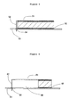
- the antenna element (11) is shown including a folded part (12) that not is located in the same plane as the other antenna element and where spacer block (13) and antenna element (11) is mounted by adhesive (14) and where adhesive (15) and protection foil (16) is applied on the spacer block.
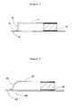
- Figure 2 illustrates a different view where the antenna element (21) has two terminals (22, 23) which are folded to create a simple connection of the radio signal.
- the spacer block (24) is smaller than the antenna element giving less material usage increased adaptively for different sizes of antennas and decrease the area used when mounted on the substrate such as printed circuit board.
- Figure 3 and 4 illustrates some other embodiments of connecting terminals.
- the insulator is by advantage embodied smaller than the antenna element and therefore use less space on, for example, a printed circuit board so the free space can be used, for example, for electrical components.
- Figure 2 illustrates a antenna element (11) and spacer block (13) that not cover the whole antenna element and that is shaped according to figure 1 . Of coarse several spacer can be applied to attain stability to the substrate they shall be mounted at. They can also have different size on the same antenna element. By that the antenna element can be big enough to give good efficiency and bandwidth but still not use to big part of the printed circuit board area and result in an excellent overall concept.
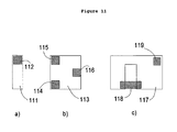
- Figure 11 shows a view where the spacer blocks position at the antenna element is shown for three different embodiments of the element.
- Figure 11a shows a smaller antenna element (111) with spacer (112)
- figure 11b shows a bigger antenna element (113) where three spacers (114, 115, 116) is placed to obtain stability
- figure 11c shows a antenna element (117) with a slot where a spacer (118) is placed to cross the slot to obtain stability and where another spacer with different size and shape (119) is placed at another position to further increase the stability.
- the positioning of the spacer is not critical, they can be placed where it is proper from different aspects. If the antenna element need a bigger separation distance to the surface than the spacer can achieve, several spacer can be attached onto each other by adhesive.
- spacer block is made of porous material containing a significant part of air to not affect the antenna properties depending on its position.
- porous material means material with dielectric constant below 2. It can also be blocks including holes that also decrease the overall dielectric constant for the block.
- the impedance match can be simplified by that the antenna element and connection pin is shaped in the same sheet of metal and the pins can be connected to each other at a plane closer to the ground plane to get a good impedance match.
- the antenna element and connection pin is shaped in the same sheet of metal and the pins can be connected to each other at a plane closer to the ground plane to get a good impedance match.
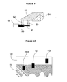
- FIG. 9 illustrates the antenna element (91), two terminals or connection pins (92, 93) having electrical connection to the ground (96) and central conductor (97) of the coaxial cable (95).
- the spacer (94) is attached by adhesive to the antenna element as shown before.
- the antenna is mounted by removing the cover or protection foil from the insulator and the antenna is pressed there it is intended to be placed on the mounting substrate.
- the antenna cover foil is removed and the adhesive (55, 65, 75, and 85) is attaching the antenna towards the substrate (53, 63, 74, 83).
- the substrate is a printed circuit board including spots intended for connection to the antenna elements terminals.
- the electrical connection can either be performed by soldering, spring loaded connection or mounting of the coaxial cables terminals either by connector or soldering.
- the soldering can either be performed in the hole where the antenna terminal is placed into, the figure 5 and 6 shows how the connection terminals (52, 62) is placed in the hole (54, 64) of the printed circuit board (53, 63) where the holes have electrical connection to the radio transmitter and/or receiver.
- the terminals can be soldered to get an electrical connection but it can also be a connection by friction force to achieve a signal transmission to the antenna element.
- Figure 6 illustrates how a smaller spacer creates a space (66) where other components can be mounted to more efficient use the board surface area.
- Figure 7 illustrates how the antenna elements (71) and terminal (72), where an extra folding creates a surface (73) that is placed onto a connection pad on the printed circuit board and thereafter is soldered.
- Figure 8 illustrates how a spring loaded connector (83) can be modelled to get a antenna (81) that by appropriate spring force get a electrical connection at the spot (84) having electrical connection to the radio transmitter and/or receiver.
- gold plating of the terminals and pads is needed to avoid bad electrical connection by oxides.
- the printed circuit board usually contains the radio transmitter and/or receiver but it isn't necessary.
- the antenna element can be mounted on a separate printed circuit board.
- the antenna element does not have to be placed on a ground-plane and can sometimes benefit to wholly or partly be placed outside of the ground plane.
- the figure 10 illustrates a printed circuit board having one part (101) not covered by a ground plane and another part (102) that is covered by a ground plane.
- the antenna can be placed at any of the positions (103, 104, 105). The antennas properties will change depending if it is placed above a ground plane or not and the antenna can need different embediment depending of placement position.
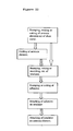
- Figure 12 illustrates a flow chart over the different step of the antenna manufacturing process according to this invention. It is obvious for a person skilled in the art that the steps can be performed in different order and that steps can be jointed and other steps in production added. Some steps don't need to be performed in production but can be done at assembly of the final product. Figure 12 is a benchmark of a possible working process only.
- Common insulators are air, different substrates for printed circuit boards, plastics and ceramics.
- Common electrical conductive materials for antenna element and ground plane are copper, silver, different alloys including the mentioned substances.
- the radio signal can, as person skilled in the art realise, be connected to the antenna element either by direct or indirect coupling.
- direct means a galvanic connection
- indirect means a capacitive or inductive coupling or a combination of both.
- this invention can be used in antenna systems including more than one antenna, for example systems for improved antenna gain, achieve space or polarization diversity or systems based on MIMO technology, meaning both transmitter and receiver having more than one antenna.
- the antenna can be used in one or more frequency bands either simultaneously or at different times.
- the antenna can have different radiation patterns by exciting different modes. It is obvious that the antenna can operate at different frequencies and excite other higher order of modes or resonance frequencies on the same antenna. This invention is not restricted to a particular mode or resonance but includes all.
- parasitic elements for example one or more layer of electric conductive material apart from the antenna element.
- the parasitic element can be shaped either to increase the antenna bandwidth or achieve a efficient antenna at a separate frequency range.
- Parasitic element can also be used for impedance matching.
Abstract
Description
- The present invention concerns an antenna that easily can be modified and mounted.
- The purpose of an antenna is to convert wire bound signals to electromagnetic signals propagating in the ambient media. The design of the antenna determines the properties of this conversion. Important parameters are antenna gain, efficiency, directivity, polarisation, bandwidth and not least physical size. The requirements of a wireless communications system determine the requirements of the antenna and by that what type of antenna to be used.
- Simple and small antennas have become attractive both because its decreased production cost and that they easily can be deployed in both fixed and mobile installations. Antennas adopted for embedding offer a low cost solution. A common group of embedded antennas is planar antennas often denominated as patch antennas. A very important parameter for patch antennas to obtain enough bandwidth is to create sufficient spacing to a ground plane in parallel.
- There are some known methods to embody planar antennas. By the denomination planar antenna means that the main part of the antenna area mainly is in parallel to and separated from a ground plane. In general the antenna element is connected to a radio transmitter and/or receiver by electrical conductors. A present common method is etching or printing an antenna shape of a foil of copper on a thin and flexible substrate of polyamide or polyester. It is denominated Flex film, which is applied by any type of adhesive on a plastic carrier that is adapted to the product and is produced by injection moulding process, and that the electrical signals are connected between the radio transmitter and antenna element by spring loaded pins. The carrier includes joints to fix the antenna on a printed circuit board and the printed circuit board has to be adapted to the carrier joints. This is a solution that primarily is suited for mass production, because the injection moulding tool is costly and that flexible films have to be produced in big quantities to achieve a low price. The flex film can be replaced by a stamped metal plate that is applied by adhesive or ultra sonic welding, but also in this case the carrier have to be adapted to each product that also implies mass production. By the denomination mass production means a quantity exceeding 100 000 units. A method that is more common for small quantity is etching of the antenna pattern in a printed circuit board of glass fibre reinforced epoxy laminate or other material intended to printed circuit board process. This method is flexible but has the limitation that cheaper material of FR4 type get an antenna with significant losses, and when the material has good electrical properties the material cost is high. A sufficient spacing between the antenna and the ground plane is also required for planar antennas to attain sufficient efficiency and bandwidth. This gives that the amount of material and therefore the cost is high.
- The method described in
US 7053833 using polymers instead of glass fibre reinforced epoxy. It is fixed by adhesive to a antenna element and also to the ground plane on opposite side by another adhesive. Thereafter an electrical conductor is elapsed through the polymer and joint by soldering to the antenna element. This method has some drawbacks. Several components and mounting process steps are needed. - The method described in
US 6675461 assign a production method for an antenna of sheet metal that are folded in such manner that a significant area is overlapping and that a spacer block is fixed between two overlapping sections. This method has more folding and use more amount of material that lead to increased cost and a more complicated production and connection to a printed circuit board than the forthcoming invention. -
US 2003 10107881 EP1378959 discloses a patch antenna which is mounted to a circuit board by adhesives. - This invention relates to a method of mounting an antenna as set out in the claim.
-
-
Figure 1 : Illustrates a side view of a complete antenna. -
Figure 2 : Antenna from another view including spacer block that not cover the whole antenna element. -
Figure 3 : Antenna having spring loaded connection pins shaped to connect without soldering. -
Figure 4 : Antenna with the connection pins bended to be mounted on connection pads, for example on top of a circuit board. -
Figure 5 : Antenna according tofigure 1 but mounted on a printed circuit board. -
Figure 6 : Antenna according tofigure 2 mounted on a printed circuit board by soldering in holes through the board. -
Figure 7 : Antenna according tofigure 4 mounted on a printed circuit board by soldering on pads on top of the printed circuit board. -
Figure 8 : Antenna according tofigure 3 mounted on a printed circuit board by connection of the signal through spring loaded connectors. -
Figure 9 : Antenna with connection through a coaxial cable. -
Figure 10 : illustrates different placements on a printed circuit board. -
Figure 11 : Illustrates different shapes and placing of spacer blocks on an antenna element. -
Figure 12 : Illustrates by an example how an antenna according to the invention can be assembled. - This invention consists of an antenna element embodied of an electrical conductive material with sufficient stiffness, for example sheet metal, and a carrier or spacer of a electrical insulator. The sheet metal is shaped to get the properties needed for the application and is manufactured by appropriate methods. Some methods is stamping, etching or cutting. One or more electrical spacer is manufactured to appropriate shape and size and an adhesive is applied onto them. Some manufacturing methods for spacer is stamping, cutting or moulding. As adhesive a material with suited properties is selected and applied with any method. The antenna element and spacer are attached together by the adhesive. On at least one of the spacers, usually all, a adhesive is applied for later assembly on the product that shall contain the antenna. The adhesive can have a protection foil to not be damaged in the handling between the antenna assembly and final mounting on the product. To get a antenna element with sufficient stiffness a electrical conductive material with thickness exceeding 50 micro meter in general is needed. Thin sheet metal of copper, silver, tin, zinc or other electrical conductive material or alloys of different material is often proper.
- It is also possible to shape connection pins, also denominated terminals, as a part of the antenna element and this part can also be folded for a simple transmission of the radio signal from of example a printed circuit board. This method offers a cheap and adaptable connection of the signal to the antenna element. By reference to
figure 1 the antenna element (11) is shown including a folded part (12) that not is located in the same plane as the other antenna element and where spacer block (13) and antenna element (11) is mounted by adhesive (14) and where adhesive (15) and protection foil (16) is applied on the spacer block.Figure 2 illustrates a different view where the antenna element (21) has two terminals (22, 23) which are folded to create a simple connection of the radio signal. The spacer block (24) is smaller than the antenna element giving less material usage increased adaptively for different sizes of antennas and decrease the area used when mounted on the substrate such as printed circuit board.Figure 3 and 4 illustrates some other embodiments of connecting terminals. - The insulator is by advantage embodied smaller than the antenna element and therefore use less space on, for example, a printed circuit board so the free space can be used, for example, for electrical components.
Figure 2 illustrates a antenna element (11) and spacer block (13) that not cover the whole antenna element and that is shaped according tofigure 1 . Of coarse several spacer can be applied to attain stability to the substrate they shall be mounted at. They can also have different size on the same antenna element. By that the antenna element can be big enough to give good efficiency and bandwidth but still not use to big part of the printed circuit board area and result in an excellent overall concept.Figure 11 shows a view where the spacer blocks position at the antenna element is shown for three different embodiments of the element.Figure 11a shows a smaller antenna element (111) with spacer (112),figure 11b shows a bigger antenna element (113) where three spacers (114, 115, 116) is placed to obtain stability andfigure 11c shows a antenna element (117) with a slot where a spacer (118) is placed to cross the slot to obtain stability and where another spacer with different size and shape (119) is placed at another position to further increase the stability. The positioning of the spacer is not critical, they can be placed where it is proper from different aspects. If the antenna element need a bigger separation distance to the surface than the spacer can achieve, several spacer can be attached onto each other by adhesive. - It is advantageous that spacer block is made of porous material containing a significant part of air to not affect the antenna properties depending on its position. By porous material means material with dielectric constant below 2. It can also be blocks including holes that also decrease the overall dielectric constant for the block.
- Since it often a demand that the electrical length and therefore the inductance between the signal and ground is less than possible achievable if the pins connects to each other at the antenna element plane, the impedance match can be simplified by that the antenna element and connection pin is shaped in the same sheet of metal and the pins can be connected to each other at a plane closer to the ground plane to get a good impedance match. By that it is possible to place the antenna element at sufficient distance from the ground plane to obtain sufficient bandwidth and by that a more robust design that fits more products without changing the antenna element shape. Also communications standards having wide bandwidth demands also require antennas having corresponding bandwidth giving need for a antenna element placed a significant distance from its mounting surface.
- If it is a cable interface to radio transmitter and/or receiver, usually of coaxial type, the antenna terminals is soldered or crimped to the cables two conductors to ensure a good electrical contact.
Figure 9 illustrates the antenna element (91), two terminals or connection pins (92, 93) having electrical connection to the ground (96) and central conductor (97) of the coaxial cable (95). The spacer (94) is attached by adhesive to the antenna element as shown before. - The antenna is mounted by removing the cover or protection foil from the insulator and the antenna is pressed there it is intended to be placed on the mounting substrate. In
figures 5, 6 ,7 and 8 the antenna cover foil is removed and the adhesive (55, 65, 75, and 85) is attaching the antenna towards the substrate (53, 63, 74, 83). Often the substrate is a printed circuit board including spots intended for connection to the antenna elements terminals. The electrical connection can either be performed by soldering, spring loaded connection or mounting of the coaxial cables terminals either by connector or soldering. The soldering can either be performed in the hole where the antenna terminal is placed into, thefigure 5 and 6 shows how the connection terminals (52, 62) is placed in the hole (54, 64) of the printed circuit board (53, 63) where the holes have electrical connection to the radio transmitter and/or receiver. The terminals can be soldered to get an electrical connection but it can also be a connection by friction force to achieve a signal transmission to the antenna element.Figure 6 illustrates how a smaller spacer creates a space (66) where other components can be mounted to more efficient use the board surface area.Figure 7 illustrates how the antenna elements (71) and terminal (72), where an extra folding creates a surface (73) that is placed onto a connection pad on the printed circuit board and thereafter is soldered.Figure 8 illustrates how a spring loaded connector (83) can be modelled to get a antenna (81) that by appropriate spring force get a electrical connection at the spot (84) having electrical connection to the radio transmitter and/or receiver. In many case gold plating of the terminals and pads is needed to avoid bad electrical connection by oxides. - The printed circuit board usually contains the radio transmitter and/or receiver but it isn't necessary. The antenna element can be mounted on a separate printed circuit board.
- The antenna element does not have to be placed on a ground-plane and can sometimes benefit to wholly or partly be placed outside of the ground plane. The
figure 10 illustrates a printed circuit board having one part (101) not covered by a ground plane and another part (102) that is covered by a ground plane. The antenna can be placed at any of the positions (103, 104, 105). The antennas properties will change depending if it is placed above a ground plane or not and the antenna can need different embediment depending of placement position. -
Figure 12 illustrates a flow chart over the different step of the antenna manufacturing process according to this invention. It is obvious for a person skilled in the art that the steps can be performed in different order and that steps can be jointed and other steps in production added. Some steps don't need to be performed in production but can be done at assembly of the final product.Figure 12 is a benchmark of a possible working process only. - Common insulators are air, different substrates for printed circuit boards, plastics and ceramics. Common electrical conductive materials for antenna element and ground plane are copper, silver, different alloys including the mentioned substances.
- The radio signal can, as person skilled in the art realise, be connected to the antenna element either by direct or indirect coupling. By direct means a galvanic connection and by indirect means a capacitive or inductive coupling or a combination of both.
- The person skilled in the art realise that this invention can be used in antenna systems including more than one antenna, for example systems for improved antenna gain, achieve space or polarization diversity or systems based on MIMO technology, meaning both transmitter and receiver having more than one antenna.
- The person skilled in the art realise that the antenna can be used in one or more frequency bands either simultaneously or at different times. The antenna can have different radiation patterns by exciting different modes. It is obvious that the antenna can operate at different frequencies and excite other higher order of modes or resonance frequencies on the same antenna. This invention is not restricted to a particular mode or resonance but includes all.
- The person skilled in the art realise that parasitic elements, for example one or more layer of electric conductive material apart from the antenna element. The parasitic element can be shaped either to increase the antenna bandwidth or achieve a efficient antenna at a separate frequency range. Parasitic element can also be used for impedance matching.
Claims (1)
- Method for mounting an antenna, the antenna comprising:- an antenna element (11) of sheet metal having a first and a second side, and a folded part (12) constituting a terminal for electrical connection of the antenna element (11) and- one or more electrical insulators (13) attached to the antenna element (11) by adhesive, wherein at least one electrical insulator having at least two sides coated with adhesive (14, 15, 55, 65, 75, 85) where at least one of the sides, or maximum one side less than the number of sides that are coated, is attached to the antenna element (11), wherein a protection foil (16) is applied to the coated side that is not attached to the antenna element (11);the method comprising the steps:- removing the protection foil (16) from the insulator (13),- pressing the antenna where it is intended to be placed on a mounting substrate (53, 63, 74, 83), thereby attaching the antenna to the mounting substrate (53, 63, 74, 83) with the adhesive (55, 65, 75, 85), and- electrically connecting the folded part (12) by any of: soldering to the mounting substrate; spring loaded connection with the mounting substrate; soldering to a coaxial cable; connection by connector to a coaxial cable.
Applications Claiming Priority (2)
| Application Number | Priority Date | Filing Date | Title |
|---|---|---|---|
| SE0601815A SE530709C2 (en) | 2006-09-04 | 2006-09-04 | Antenna manufacturing method |
| PCT/SE2007/000767 WO2008030159A1 (en) | 2006-09-04 | 2007-09-03 | Antenna |
Publications (3)
| Publication Number | Publication Date |
|---|---|
| EP2059971A1 EP2059971A1 (en) | 2009-05-20 |
| EP2059971A4 EP2059971A4 (en) | 2009-11-18 |
| EP2059971B1 true EP2059971B1 (en) | 2011-08-10 |
Family
ID=39157496
Family Applications (1)
| Application Number | Title | Priority Date | Filing Date |
|---|---|---|---|
| EP07808787A Not-in-force EP2059971B1 (en) | 2006-09-04 | 2007-09-03 | Antenna |
Country Status (5)
| Country | Link |
|---|---|
| US (1) | US20100188292A1 (en) |
| EP (1) | EP2059971B1 (en) |
| AT (1) | ATE520168T1 (en) |
| SE (1) | SE530709C2 (en) |
| WO (1) | WO2008030159A1 (en) |
Families Citing this family (9)
| Publication number | Priority date | Publication date | Assignee | Title |
|---|---|---|---|---|
| WO2010138856A1 (en) | 2009-05-29 | 2010-12-02 | Abbott Diabetes Care Inc. | Medical device antenna systems having external antenna configurations |
| US20140028501A1 (en) * | 2012-07-27 | 2014-01-30 | Logitech Europe S.A. | 3-d antenna for wireless communications |
| WO2014021977A1 (en) * | 2012-07-30 | 2014-02-06 | Utc Fire & Security Americas Corporation, Inc. | Ism band antenna structure for security system |
| WO2016144039A1 (en) | 2015-03-06 | 2016-09-15 | Samsung Electronics Co., Ltd. | Circuit element package, manufacturing method thereof, and manufacturing apparatus thereof |
| US10477737B2 (en) | 2016-05-04 | 2019-11-12 | Samsung Electronics Co., Ltd. | Manufacturing method of a hollow shielding structure for circuit elements |
| US10477687B2 (en) | 2016-08-04 | 2019-11-12 | Samsung Electronics Co., Ltd. | Manufacturing method for EMI shielding structure |
| KR102551657B1 (en) | 2016-12-12 | 2023-07-06 | 삼성전자주식회사 | EMI shielding structure and manufacturing method for the same |
| US10594020B2 (en) * | 2017-07-19 | 2020-03-17 | Samsung Electronics Co., Ltd. | Electronic device having antenna element and method for manufacturing the same |
| KR102373931B1 (en) | 2017-09-08 | 2022-03-14 | 삼성전자주식회사 | Electromagnetic interference shielding structure |
Family Cites Families (7)
| Publication number | Priority date | Publication date | Assignee | Title |
|---|---|---|---|---|
| US5155493A (en) * | 1990-08-28 | 1992-10-13 | The United States Of America As Represented By The Secretary Of The Air Force | Tape type microstrip patch antenna |
| WO2001037366A1 (en) * | 1999-11-15 | 2001-05-25 | Motorola, Inc. | Deformable patch antenna |
| US6675461B1 (en) * | 2001-06-26 | 2004-01-13 | Ethertronics, Inc. | Method for manufacturing a magnetic dipole antenna |
| US6703114B1 (en) * | 2002-10-17 | 2004-03-09 | Arlon | Laminate structures, methods for production thereof and uses therefor |
| EP1445823B1 (en) * | 2003-02-10 | 2007-06-13 | Sony Ericsson Mobile Communications AB | Combined speaker and antenna component |
| GB2404497A (en) * | 2003-07-30 | 2005-02-02 | Peter Bryan Webster | PCB mounted antenna |
| US7053833B2 (en) * | 2004-07-22 | 2006-05-30 | Wistron Neweb Corporation | Patch antenna utilizing a polymer dielectric layer |
-
2006
- 2006-09-04 SE SE0601815A patent/SE530709C2/en not_active IP Right Cessation
-
2007
- 2007-09-03 US US12/310,633 patent/US20100188292A1/en not_active Abandoned
- 2007-09-03 EP EP07808787A patent/EP2059971B1/en not_active Not-in-force
- 2007-09-03 AT AT07808787T patent/ATE520168T1/en not_active IP Right Cessation
- 2007-09-03 WO PCT/SE2007/000767 patent/WO2008030159A1/en active Application Filing
Also Published As
| Publication number | Publication date |
|---|---|
| EP2059971A4 (en) | 2009-11-18 |
| SE530709C2 (en) | 2008-08-19 |
| SE0601815L (en) | 2008-03-05 |
| ATE520168T1 (en) | 2011-08-15 |
| US20100188292A1 (en) | 2010-07-29 |
| WO2008030159A1 (en) | 2008-03-13 |
| EP2059971A1 (en) | 2009-05-20 |
Similar Documents
| Publication | Publication Date | Title |
|---|---|---|
| EP2059971B1 (en) | Antenna | |
| CN100514748C (en) | Antenna module and elctronic apparatus having the same | |
| EP3490067B1 (en) | Substrate for rfid tags, rfid tag and rfid system | |
| US7775446B2 (en) | Card type information device and method for manufacturing same | |
| US9356366B2 (en) | Cable connector assembly for a communication system | |
| KR101320205B1 (en) | Antenna device and radio communication device using same | |
| CN102437412B (en) | Wireless communication system | |
| CN102544754B (en) | Mimo antenna equipment and wireless terminal | |
| EP2251929B1 (en) | Wideband antenna and clothing and articles using the same | |
| WO1998049743A1 (en) | Antenna for radio communications apparatus | |
| CN102377045A (en) | Electronic device having transmission line pattern embedded in case and method for manufacturing the same | |
| CN206727226U (en) | Antenna assembly and electronic equipment | |
| TW200952253A (en) | Antenna assembly, printed wiring board and device | |
| EP3709610B1 (en) | Mobile terminal and method for manufacturing antenna thereof | |
| KR101153165B1 (en) | High frequency transmission line using printed circuit board | |
| US8051550B2 (en) | Method for mounting a tridimensional antenna | |
| EP2394331A1 (en) | Antenna | |
| CN100379081C (en) | Hidden type antenna assembly in multifrequency | |
| US7586449B1 (en) | Antenna structure and method for manufacturing the antenna structure | |
| JP4671446B2 (en) | Electromagnetic induction module | |
| EP2171800B1 (en) | Antenna assembly | |
| US7692589B2 (en) | Antenna device, electronic device, and method of manufacturing antenna device | |
| KR20150024244A (en) | Flexible Intenna | |
| CN212934846U (en) | PCB for communication antenna | |
| CN212412195U (en) | Low-frequency oscillator structure and base station antenna |
Legal Events
| Date | Code | Title | Description |
|---|---|---|---|
| PUAI | Public reference made under article 153(3) epc to a published international application that has entered the european phase |
Free format text: ORIGINAL CODE: 0009012 |
|
| 17P | Request for examination filed |
Effective date: 20081219 |
|
| AK | Designated contracting states |
Kind code of ref document: A1 Designated state(s): AT BE BG CH CY CZ DE DK EE ES FI FR GB GR HU IE IS IT LI LT LU LV MC MT NL PL PT RO SE SI SK TR |
|
| AX | Request for extension of the european patent |
Extension state: AL BA HR MK RS |
|
| A4 | Supplementary search report drawn up and despatched |
Effective date: 20091021 |
|
| RIC1 | Information provided on ipc code assigned before grant |
Ipc: H01Q 1/24 20060101AFI20080410BHEP Ipc: H01Q 1/38 20060101ALI20091015BHEP |
|
| 17Q | First examination report despatched |
Effective date: 20100203 |
|
| GRAP | Despatch of communication of intention to grant a patent |
Free format text: ORIGINAL CODE: EPIDOSNIGR1 |
|
| DAX | Request for extension of the european patent (deleted) | ||
| GRAS | Grant fee paid |
Free format text: ORIGINAL CODE: EPIDOSNIGR3 |
|
| GRAA | (expected) grant |
Free format text: ORIGINAL CODE: 0009210 |
|
| AK | Designated contracting states |
Kind code of ref document: B1 Designated state(s): AT BE BG CH CY CZ DE DK EE ES FI FR GB GR HU IE IS IT LI LT LU LV MC MT NL PL PT RO SE SI SK TR |
|
| REG | Reference to a national code |
Ref country code: GB Ref legal event code: FG4D |
|
| REG | Reference to a national code |
Ref country code: CH Ref legal event code: EP |
|
| REG | Reference to a national code |
Ref country code: IE Ref legal event code: FG4D |
|
| REG | Reference to a national code |
Ref country code: DE Ref legal event code: R096 Ref document number: 602007016476 Country of ref document: DE Effective date: 20111013 |
|
| REG | Reference to a national code |
Ref country code: NL Ref legal event code: VDEP Effective date: 20110810 |
|
| RAP2 | Party data changed (patent owner data changed or rights of a patent transferred) |
Owner name: PROANT AB |
|
| LTIE | Lt: invalidation of european patent or patent extension |
Effective date: 20110810 |
|
| PG25 | Lapsed in a contracting state [announced via postgrant information from national office to epo] |
Ref country code: LT Free format text: LAPSE BECAUSE OF FAILURE TO SUBMIT A TRANSLATION OF THE DESCRIPTION OR TO PAY THE FEE WITHIN THE PRESCRIBED TIME-LIMIT Effective date: 20110810 Ref country code: SE Free format text: LAPSE BECAUSE OF FAILURE TO SUBMIT A TRANSLATION OF THE DESCRIPTION OR TO PAY THE FEE WITHIN THE PRESCRIBED TIME-LIMIT Effective date: 20110810 Ref country code: IS Free format text: LAPSE BECAUSE OF FAILURE TO SUBMIT A TRANSLATION OF THE DESCRIPTION OR TO PAY THE FEE WITHIN THE PRESCRIBED TIME-LIMIT Effective date: 20111210 Ref country code: FI Free format text: LAPSE BECAUSE OF FAILURE TO SUBMIT A TRANSLATION OF THE DESCRIPTION OR TO PAY THE FEE WITHIN THE PRESCRIBED TIME-LIMIT Effective date: 20110810 Ref country code: PT Free format text: LAPSE BECAUSE OF FAILURE TO SUBMIT A TRANSLATION OF THE DESCRIPTION OR TO PAY THE FEE WITHIN THE PRESCRIBED TIME-LIMIT Effective date: 20111212 Ref country code: NL Free format text: LAPSE BECAUSE OF FAILURE TO SUBMIT A TRANSLATION OF THE DESCRIPTION OR TO PAY THE FEE WITHIN THE PRESCRIBED TIME-LIMIT Effective date: 20110810 |
|
| REG | Reference to a national code |
Ref country code: AT Ref legal event code: MK05 Ref document number: 520168 Country of ref document: AT Kind code of ref document: T Effective date: 20110810 |
|
| PG25 | Lapsed in a contracting state [announced via postgrant information from national office to epo] |
Ref country code: SI Free format text: LAPSE BECAUSE OF FAILURE TO SUBMIT A TRANSLATION OF THE DESCRIPTION OR TO PAY THE FEE WITHIN THE PRESCRIBED TIME-LIMIT Effective date: 20110810 Ref country code: AT Free format text: LAPSE BECAUSE OF FAILURE TO SUBMIT A TRANSLATION OF THE DESCRIPTION OR TO PAY THE FEE WITHIN THE PRESCRIBED TIME-LIMIT Effective date: 20110810 Ref country code: LV Free format text: LAPSE BECAUSE OF FAILURE TO SUBMIT A TRANSLATION OF THE DESCRIPTION OR TO PAY THE FEE WITHIN THE PRESCRIBED TIME-LIMIT Effective date: 20110810 Ref country code: GR Free format text: LAPSE BECAUSE OF FAILURE TO SUBMIT A TRANSLATION OF THE DESCRIPTION OR TO PAY THE FEE WITHIN THE PRESCRIBED TIME-LIMIT Effective date: 20111111 Ref country code: PL Free format text: LAPSE BECAUSE OF FAILURE TO SUBMIT A TRANSLATION OF THE DESCRIPTION OR TO PAY THE FEE WITHIN THE PRESCRIBED TIME-LIMIT Effective date: 20110810 Ref country code: CY Free format text: LAPSE BECAUSE OF FAILURE TO SUBMIT A TRANSLATION OF THE DESCRIPTION OR TO PAY THE FEE WITHIN THE PRESCRIBED TIME-LIMIT Effective date: 20110810 |
|
| PG25 | Lapsed in a contracting state [announced via postgrant information from national office to epo] |
Ref country code: BE Free format text: LAPSE BECAUSE OF FAILURE TO SUBMIT A TRANSLATION OF THE DESCRIPTION OR TO PAY THE FEE WITHIN THE PRESCRIBED TIME-LIMIT Effective date: 20110810 |
|
| PG25 | Lapsed in a contracting state [announced via postgrant information from national office to epo] |
Ref country code: MC Free format text: LAPSE BECAUSE OF NON-PAYMENT OF DUE FEES Effective date: 20110930 Ref country code: SK Free format text: LAPSE BECAUSE OF FAILURE TO SUBMIT A TRANSLATION OF THE DESCRIPTION OR TO PAY THE FEE WITHIN THE PRESCRIBED TIME-LIMIT Effective date: 20110810 Ref country code: CZ Free format text: LAPSE BECAUSE OF FAILURE TO SUBMIT A TRANSLATION OF THE DESCRIPTION OR TO PAY THE FEE WITHIN THE PRESCRIBED TIME-LIMIT Effective date: 20110810 |
|
| REG | Reference to a national code |
Ref country code: CH Ref legal event code: PL |
|
| PG25 | Lapsed in a contracting state [announced via postgrant information from national office to epo] |
Ref country code: RO Free format text: LAPSE BECAUSE OF FAILURE TO SUBMIT A TRANSLATION OF THE DESCRIPTION OR TO PAY THE FEE WITHIN THE PRESCRIBED TIME-LIMIT Effective date: 20110810 Ref country code: EE Free format text: LAPSE BECAUSE OF FAILURE TO SUBMIT A TRANSLATION OF THE DESCRIPTION OR TO PAY THE FEE WITHIN THE PRESCRIBED TIME-LIMIT Effective date: 20110810 |
|
| PLBE | No opposition filed within time limit |
Free format text: ORIGINAL CODE: 0009261 |
|
| STAA | Information on the status of an ep patent application or granted ep patent |
Free format text: STATUS: NO OPPOSITION FILED WITHIN TIME LIMIT |
|
| REG | Reference to a national code |
Ref country code: IE Ref legal event code: MM4A |
|
| PG25 | Lapsed in a contracting state [announced via postgrant information from national office to epo] |
Ref country code: DK Free format text: LAPSE BECAUSE OF FAILURE TO SUBMIT A TRANSLATION OF THE DESCRIPTION OR TO PAY THE FEE WITHIN THE PRESCRIBED TIME-LIMIT Effective date: 20110810 |
|
| 26N | No opposition filed |
Effective date: 20120511 |
|
| PG25 | Lapsed in a contracting state [announced via postgrant information from national office to epo] |
Ref country code: LI Free format text: LAPSE BECAUSE OF NON-PAYMENT OF DUE FEES Effective date: 20110930 Ref country code: IE Free format text: LAPSE BECAUSE OF NON-PAYMENT OF DUE FEES Effective date: 20110903 Ref country code: CH Free format text: LAPSE BECAUSE OF NON-PAYMENT OF DUE FEES Effective date: 20110930 |
|
| REG | Reference to a national code |
Ref country code: DE Ref legal event code: R097 Ref document number: 602007016476 Country of ref document: DE Effective date: 20120511 |
|
| PG25 | Lapsed in a contracting state [announced via postgrant information from national office to epo] |
Ref country code: MT Free format text: LAPSE BECAUSE OF FAILURE TO SUBMIT A TRANSLATION OF THE DESCRIPTION OR TO PAY THE FEE WITHIN THE PRESCRIBED TIME-LIMIT Effective date: 20110810 |
|
| PG25 | Lapsed in a contracting state [announced via postgrant information from national office to epo] |
Ref country code: ES Free format text: LAPSE BECAUSE OF FAILURE TO SUBMIT A TRANSLATION OF THE DESCRIPTION OR TO PAY THE FEE WITHIN THE PRESCRIBED TIME-LIMIT Effective date: 20111121 |
|
| PG25 | Lapsed in a contracting state [announced via postgrant information from national office to epo] |
Ref country code: LU Free format text: LAPSE BECAUSE OF NON-PAYMENT OF DUE FEES Effective date: 20110903 |
|
| PG25 | Lapsed in a contracting state [announced via postgrant information from national office to epo] |
Ref country code: BG Free format text: LAPSE BECAUSE OF FAILURE TO SUBMIT A TRANSLATION OF THE DESCRIPTION OR TO PAY THE FEE WITHIN THE PRESCRIBED TIME-LIMIT Effective date: 20111110 |
|
| PG25 | Lapsed in a contracting state [announced via postgrant information from national office to epo] |
Ref country code: TR Free format text: LAPSE BECAUSE OF FAILURE TO SUBMIT A TRANSLATION OF THE DESCRIPTION OR TO PAY THE FEE WITHIN THE PRESCRIBED TIME-LIMIT Effective date: 20110810 |
|
| PG25 | Lapsed in a contracting state [announced via postgrant information from national office to epo] |
Ref country code: HU Free format text: LAPSE BECAUSE OF FAILURE TO SUBMIT A TRANSLATION OF THE DESCRIPTION OR TO PAY THE FEE WITHIN THE PRESCRIBED TIME-LIMIT Effective date: 20110810 |
|
| REG | Reference to a national code |
Ref country code: FR Ref legal event code: PLFP Year of fee payment: 9 |
|
| PGFP | Annual fee paid to national office [announced via postgrant information from national office to epo] |
Ref country code: DE Payment date: 20150922 Year of fee payment: 9 Ref country code: GB Payment date: 20150917 Year of fee payment: 9 |
|
| PGFP | Annual fee paid to national office [announced via postgrant information from national office to epo] |
Ref country code: FR Payment date: 20150922 Year of fee payment: 9 |
|
| PGFP | Annual fee paid to national office [announced via postgrant information from national office to epo] |
Ref country code: IT Payment date: 20150924 Year of fee payment: 9 |
|
| REG | Reference to a national code |
Ref country code: DE Ref legal event code: R119 Ref document number: 602007016476 Country of ref document: DE |
|
| GBPC | Gb: european patent ceased through non-payment of renewal fee |
Effective date: 20160903 |
|
| REG | Reference to a national code |
Ref country code: FR Ref legal event code: ST Effective date: 20170531 |
|
| PG25 | Lapsed in a contracting state [announced via postgrant information from national office to epo] |
Ref country code: GB Free format text: LAPSE BECAUSE OF NON-PAYMENT OF DUE FEES Effective date: 20160903 Ref country code: DE Free format text: LAPSE BECAUSE OF NON-PAYMENT OF DUE FEES Effective date: 20170401 Ref country code: FR Free format text: LAPSE BECAUSE OF NON-PAYMENT OF DUE FEES Effective date: 20160930 |
|
| PG25 | Lapsed in a contracting state [announced via postgrant information from national office to epo] |
Ref country code: IT Free format text: LAPSE BECAUSE OF NON-PAYMENT OF DUE FEES Effective date: 20160903 |