EP2059101B1 - Power line arrangement - Google Patents
Power line arrangement Download PDFInfo
- Publication number
- EP2059101B1 EP2059101B1 EP08019262.8A EP08019262A EP2059101B1 EP 2059101 B1 EP2059101 B1 EP 2059101B1 EP 08019262 A EP08019262 A EP 08019262A EP 2059101 B1 EP2059101 B1 EP 2059101B1
- Authority
- EP
- European Patent Office
- Prior art keywords
- power line
- power
- power lines
- lines
- current
- Prior art date
- Legal status (The legal status is an assumption and is not a legal conclusion. Google has not performed a legal analysis and makes no representation as to the accuracy of the status listed.)
- Active
Links
Images



Classifications
-
- H—ELECTRICITY
- H01—ELECTRIC ELEMENTS
- H01R—ELECTRICALLY-CONDUCTIVE CONNECTIONS; STRUCTURAL ASSOCIATIONS OF A PLURALITY OF MUTUALLY-INSULATED ELECTRICAL CONNECTING ELEMENTS; COUPLING DEVICES; CURRENT COLLECTORS
- H01R13/00—Details of coupling devices of the kinds covered by groups H01R12/70 or H01R24/00 - H01R33/00
- H01R13/646—Details of coupling devices of the kinds covered by groups H01R12/70 or H01R24/00 - H01R33/00 specially adapted for high-frequency, e.g. structures providing an impedance match or phase match
-
- H—ELECTRICITY
- H05—ELECTRIC TECHNIQUES NOT OTHERWISE PROVIDED FOR
- H05K—PRINTED CIRCUITS; CASINGS OR CONSTRUCTIONAL DETAILS OF ELECTRIC APPARATUS; MANUFACTURE OF ASSEMBLAGES OF ELECTRICAL COMPONENTS
- H05K1/00—Printed circuits
- H05K1/02—Details
- H05K1/0213—Electrical arrangements not otherwise provided for
- H05K1/0216—Reduction of cross-talk, noise or electromagnetic interference
- H05K1/0228—Compensation of cross-talk by a mutually correlated lay-out of printed circuit traces, e.g. for compensation of cross-talk in mounted connectors
-
- G—PHYSICS
- G05—CONTROLLING; REGULATING
- G05F—SYSTEMS FOR REGULATING ELECTRIC OR MAGNETIC VARIABLES
- G05F1/00—Automatic systems in which deviations of an electric quantity from one or more predetermined values are detected at the output of the system and fed back to a device within the system to restore the detected quantity to its predetermined value or values, i.e. retroactive systems
- G05F1/10—Regulating voltage or current
-
- H—ELECTRICITY
- H02—GENERATION; CONVERSION OR DISTRIBUTION OF ELECTRIC POWER
- H02M—APPARATUS FOR CONVERSION BETWEEN AC AND AC, BETWEEN AC AND DC, OR BETWEEN DC AND DC, AND FOR USE WITH MAINS OR SIMILAR POWER SUPPLY SYSTEMS; CONVERSION OF DC OR AC INPUT POWER INTO SURGE OUTPUT POWER; CONTROL OR REGULATION THEREOF
- H02M1/00—Details of apparatus for conversion
- H02M1/12—Arrangements for reducing harmonics from AC input or output
-
- H—ELECTRICITY
- H05—ELECTRIC TECHNIQUES NOT OTHERWISE PROVIDED FOR
- H05K—PRINTED CIRCUITS; CASINGS OR CONSTRUCTIONAL DETAILS OF ELECTRIC APPARATUS; MANUFACTURE OF ASSEMBLAGES OF ELECTRICAL COMPONENTS
- H05K1/00—Printed circuits
- H05K1/02—Details
- H05K1/0213—Electrical arrangements not otherwise provided for
- H05K1/0237—High frequency adaptations
- H05K1/0245—Lay-out of balanced signal pairs, e.g. differential lines or twisted lines
-
- H—ELECTRICITY
- H05—ELECTRIC TECHNIQUES NOT OTHERWISE PROVIDED FOR
- H05K—PRINTED CIRCUITS; CASINGS OR CONSTRUCTIONAL DETAILS OF ELECTRIC APPARATUS; MANUFACTURE OF ASSEMBLAGES OF ELECTRICAL COMPONENTS
- H05K2201/00—Indexing scheme relating to printed circuits covered by H05K1/00
- H05K2201/09—Shape and layout
- H05K2201/09209—Shape and layout details of conductors
- H05K2201/09218—Conductive traces
- H05K2201/09263—Meander
-
- H—ELECTRICITY
- H05—ELECTRIC TECHNIQUES NOT OTHERWISE PROVIDED FOR
- H05K—PRINTED CIRCUITS; CASINGS OR CONSTRUCTIONAL DETAILS OF ELECTRIC APPARATUS; MANUFACTURE OF ASSEMBLAGES OF ELECTRICAL COMPONENTS
- H05K2201/00—Indexing scheme relating to printed circuits covered by H05K1/00
- H05K2201/09—Shape and layout
- H05K2201/09209—Shape and layout details of conductors
- H05K2201/09654—Shape and layout details of conductors covering at least two types of conductors provided for in H05K2201/09218 - H05K2201/095
- H05K2201/097—Alternating conductors, e.g. alternating different shaped pads, twisted pairs; Alternating components
Definitions
- One or more embodiments described herein relate to power lines.
- Common-mode noise can radiate from a power line between inputs of board-mounted devices and ground.
- Common-mode noise is a leading cause electromagnetic interference (EMI), which propagates between devices along power and other circuit lines.
- United States Patent Application Publication US 2005/0093642 discloses a first power line and a second power line which cross one another in a twisted pattern. The ends of the two power lines are coupled to different power lines. That is, the first power line is coupled to an LD driving output circuit and the second power line is coupled to ground through a capacitor.
- United States Patent Application Publication US 2003/0189471 discloses a first coil and a second coil tapped off one line of a pair of balanced lines, the first and second coils cross at least once and together provide an inductive coupling to ground for the respective balanced line.
- the present invention provides a power line arrangement in accordance with claim 1. Preferred embodiments are defined in the dependent claims.
- Figure 1 shows one embodiment of a power line 10 having two ends 11 and 14. From end 11, a pair of power lines 12 and 13 branch off and extend in different (e.g., opposing) directions. Power lines 12 and 13 may have one or more common properties, e.g., resistance. As further shown in Figure 1 , at least one cross area A is formed between power lines 12 and 13. The directions in which current flows in the power lines may be different. This may be accomplished by aligning the power lines in a manner which allows the different current directions to be formed at the cross area. Also, power lines 12 and 13 may be aligned in two or three dimensions so as to form opposing current directions at the cross area.
- the power lines may have a chain or twist shape but they do not necessarily contact each other in this area.
- power lines 12 and 13 branch off from end 11, meet at cross area A, and extend away again to escape the cross area A.
- the two power lines meet and are coupled, for example, to a power input of an electronic device element or are grounded.
- end 11 of power line 10 is coupled to a direct current (DC) power supply.
- DC direct current
- noise components e.g., common-mode noise and EMI
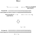
- Figure 2 illustrates one principle of how noise (and EMI) can be reduced or eliminated in the power line of Figure 1 .
- the direction of current i 1 flowing through power line 12 in cross area A is defined as the "+" direction
- the direction of current i 2 flowing through power line 13 has an opposite direction, i.e., the "-" direction.
- common-mode noise components n 21 and n 12 are generated on/by power lines 12 and 13, respectively, due to currents i 2 and i 1 . That is, common-mode noise component n 21 generated by current i 2 flowing through power line 13 is induced on power line 12, through which current i 1 flows.
- common-mode noise component n 12 generated by current ii through power line 13 is induced on second power line 13, through which current i 2 flows. Because these noise-components are equal (or at least substantially so) and opposite, they reduce or cancel one another out in each power line.
- n 12 kn c 1
- coupling coefficient "k" depends on the widths of and distances between the power lines.
- the coupling coefficient k may be arbitrarily set within a range from 0 to 1 (0 ⁇ k ⁇ 1).
- the coupling coefficient k may be set to become larger.
- the distance between the lines may have more effect on the coupling coefficient than the widths of the lines.
- n r2 1 ⁇ k n c 2
- power line 10 may have a plurality of cross areas.
- noise reduction or elimination results in each cross area based on the aforementioned principles.
- N cross areas N >1
- total noise reduction n r2 of power line 13 can be expressed by Equation 4.
- n r 2 1 ⁇ k ⁇ 1 ⁇ k ⁇ 1 ⁇ k ... ⁇ 1 ⁇ k
- n c 2 1 ⁇ k N n c 2
- power lines 12 and 13 may or may not be parallel to each other.
- power lines 12 and 13 may be parallel to one another, and in one or more other cross areas power lines 12 and 13 may not be parallel to one another.
- Figure 3A shows an EMI radiation pattern generated by a conventional power line, e.g., one that does not have cross areas
- Figure 3B shows an EMI radiation pattern generated by a power line formed in accordance with one or more embodiments previously described.
- the conventional power line radiates 95.3 V/m of EMI.
- a maximum intensity of EMI radiated from power line 10 is merely 4.63 V/m.
- a power line formed according to the embodiments described herein achieves a significant reduction in EMI compared with a conventional power line.
- common-mode noise may be substantially reduced as a result of current flowing in different or opposite directions at every cross area. As the number of cross areas increases, the adverse effects produced by common-mode noise (and its associated EMI) are remarkably reduced.
- the power lines are shown to be separated by a predetermined distance "d" in the cross area.
- d a predetermined distance
- an elevation in noise reduction may be realized when the power lines are closer to one another.
- Figure 4 one arrangement of connections between power line 10 and one or more elements 30, which, for example, may be one or more electronic devices mounted on a common plane or circuit board 100. While Figure 4 shows the connection of a power line having a plurality of cross areas, this similar connections may be formed for a power line having only one cross area as shown in Figure 1 .
- power line 10 includes a main power line 15 and at least one sub-power line 16.
- the main power line is formed from a pair of main power lines, 15b and 15c, which branch off from one end 15a of power line 10.
- the main power lines may be connected to a power supply and may extend away from each other at the branch point.
- the main power lines are disposed in a twisted or chained form having at least one cross area. In each cross area, current flows in different or opposite directions as a result of the twisted or chain arrangement.
- the main power lines recombine at end 15d, which, for example, may terminate with a constant resistance or which may be left opened according to requirement of the overall device or board.
- Each sub-power line 16 provides a current path between the main power lines 15b and 15c and a respective one of elements 30.
- Each sub-power line may also be formed from a pair of sub-power lines.
- sub-power lines 16b and 16c may respectively extend from branch points 15e and 15f in main power lines 15b and 15c.
- the sub-power lines 16b and 16c have at least one cross area, where current in the sub-power lines flow in different or opposite directions.
- the sub-power lines 16b and 16c recombine at end 16d, which, for example, may be connected to a power input of element 31.
- the main power line 15 may be connected to the other elements 32 and 33 by sub-power line pairs similar to the ones connected to element 31 or a different sub-power line arrangement may be used.
- elements 31 to 33 may be mounted in different regions 101 to 103 of the same plane of board 100.
- End 15a of the main power line may be coupled to a power supply and end 15d may be coupled to ground or a termination component or element.
- the elements may be formed on different layers or planes or on different circuit boards.
- elements 31a and 32a may be mounted on different layers 101a and 102a, respectively, and main power line 15 may be configured on another layer 104.
- main power line 15 may be configured on layer 101a or 102a where element 31a or 31b is mounted.
- Each sub-power line 16 may be formed on a respective one of layers 101a and 102a to connect corresponding elements to the main power line.
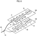
- Figure 6 shows an arrangement in which elements 34 and 35 are mounted on different boards 105 and 106 and connected to a power line 20.
- the power line 20 branches off into power lines 21 and line 22. If power line 20 is a power line coupled to a main power line which is coupled to a power supply, then power lines 21 and 22 may be considered sub-power lines. Alternatively, power line 20 may be connected directly to a power supply.
- Power lines 21 and 22 branch off at end 23 to respectively provide power to elements 34 and 35 mounted on different boards 105 and 106.
- Boards 105 and 106 may be aligned so as to define one or more cross regions R relative to power lines 21 and 22.
- the directions of the currents i 3 and i 4 flowing in these lines at the cross areas are different or opposite to one another.
- common-mode noise components (and attendant EMI) generated by currents i 3 and i 4 can be reduced or eliminated according to the principles previously described.
- each power line effectively functions as a common-mode noise filter at the cross regions.
- induction of common-mode noise from the power lines can be efficiently prevented.
- manufacturing cost and complexity can be substantially reduced compared with conventional methods.
- a board that incorporates a power-line arrangement according to the embodiments described herein can prevent EMI from adversely affecting electronic devices connected to or in the vicinity of the power lines, thereby ensuring stable operation. Further, EMI radiation from the power lines can be reduced, thereby further ensuring stable operation.
- any reference in this specification to "one embodiment,” “an embodiment,” “example embodiment,” etc. means that a particular feature, structure or characteristic described in connection with the embodiment is included in at least one embodiment of the present invention.
- the appearances of such phrases in various places in the specification are not necessarily all referring to the same embodiment.
Landscapes
- Engineering & Computer Science (AREA)
- Physics & Mathematics (AREA)
- Electromagnetism (AREA)
- Microelectronics & Electronic Packaging (AREA)
- Power Engineering (AREA)
- General Physics & Mathematics (AREA)
- Radar, Positioning & Navigation (AREA)
- Automation & Control Theory (AREA)
- Structure Of Printed Boards (AREA)
- Shielding Devices Or Components To Electric Or Magnetic Fields (AREA)
- Semiconductor Integrated Circuits (AREA)
Description
- One or more embodiments described herein relate to power lines.
- Many electronic devices on a circuit board have inputs coupled to a power line. Clock generators and DC-DC converters are examples of these devices. Power lines can serve as a source of noise under certain circumstances. For example, one type of noise known as common-mode noise can radiate from a power line between inputs of board-mounted devices and ground. Common-mode noise is a leading cause electromagnetic interference (EMI), which propagates between devices along power and other circuit lines.
- Attempts have been made to reduce the EMI generated by common-mode noise. One technique involves forming each power line as a single strip. This technique has proven ineffective and, in fact, can induce the generation of standing waves that increase the adverse effective of common-mode noise-generated EMI.
- United States Patent Application Publication
US 2005/0093642 discloses a first power line and a second power line which cross one another in a twisted pattern. The ends of the two power lines are coupled to different power lines. That is, the first power line is coupled to an LD driving output circuit and the second power line is coupled to ground through a capacitor. United States Patent Application PublicationUS 2003/0189471 discloses a first coil and a second coil tapped off one line of a pair of balanced lines, the first and second coils cross at least once and together provide an inductive coupling to ground for the respective balanced line. - The present invention provides a power line arrangement in accordance with claim 1. Preferred embodiments are defined in the dependent claims.
- The embodiments will be described in detail with reference to the following drawings in which like reference numerals refer to like elements wherein:
-
Figure 1 is a diagram of one embodiment of a power line arrangement. -
Figure 2 is a conceptual diagram illustrating a principle of noise reduction that may be achieved in the power line arrangement ofFigure 1 . -
Figure 3A shows an EMI radiation pattern on another type of power line, andFigure 3B shows and an EMI radiation pattern that may be generated by the power line arrangement ofFigure 1 . -
Figure 4 is a diagram showing one arrangement of connections between one or more power lines formed according to the embodiment ofFigure 1 and other electronic devices. -
Figure 5 is a diagram showing another arrangement of connections between one or more power lines formed according to the embodiment ofFigure 1 and other electronic devices. -
Figure. 6 is a diagram showing another arrangement of connections between one or more power lines formed according to the embodiment ofFigure 1 and other electronic devices. -
Figure 1 shows one embodiment of apower line 10 having twoends end 11, a pair ofpower lines Power lines Figure 1 , at least one cross area A is formed betweenpower lines power lines - At cross area A, the power lines may have a chain or twist shape but they do not necessarily contact each other in this area. For example,
power lines end 11, meet at cross area A, and extend away again to escape the cross area A. At theother end 14, the two power lines meet and are coupled, for example, to a power input of an electronic device element or are grounded. - In terms of signal propagation, from
end 11 current it is divided into currents i1 and i2 that flow respectively throughpower lines power lines - According to one embodiment,
end 11 ofpower line 10 is coupled to a direct current (DC) power supply. As a result, DC current will flow intopower lines -
Figure 2 illustrates one principle of how noise (and EMI) can be reduced or eliminated in the power line ofFigure 1 . If the direction of current i1 flowing throughpower line 12 in cross area A is defined as the "+" direction, then the direction of current i2 flowing throughpower line 13 has an opposite direction, i.e., the "-" direction. In cross area A, common-mode noise components n21 and n12 are generated on/bypower lines power line 13 is induced onpower line 12, through which current i1 flows. Likewise, common-mode noise component n12 generated by current ii throughpower line 13 is induced onsecond power line 13, through which current i2 flows. Because these noise-components are equal (or at least substantially so) and opposite, they reduce or cancel one another out in each power line. - The relationship between common-mode noise components n12 and n12 induced on
power lines 
- In Equation 1, coupling coefficient "k" depends on the widths of and distances between the power lines. In accordance with one embodiment, the coupling coefficient k may be arbitrarily set within a range from 0 to 1 (0 < k < 1). Alternatively, as the distance between the power lines becomes smaller and the widths of power lines become narrower, the coupling coefficient k may be set to become larger. Also, the distance between the lines may have more effect on the coupling coefficient than the widths of the lines. Thus, the amount of noise cancelled in a power line by the noise induced from the other power line is proportioned to the spacing between the power lines at the cross area(s). Furthermore, the amount of noise cancelled in a power line by the noise induced from the other power line is proportional to the widths of the power lines.
- In cross area A, the noise in
second power line 13 is reduced as much as nr2 as defined in Equation 2:
- If the power lines have the same resistance, and nc2 becomes equal to nc1 (nc2 = nc1), then the noise reduction nr2 can be provided as Equation 3.

- From Equation 3, it is apparent that, in cross area A, common-mode noise of
power line 13 may be reduced as much as (1-k) times. Common-mode noise ofpower line 12 may be reduced in a similar manner. Consequently, the noise nr1 ofpower line 12 and the noise nr2 ofpower line 13 may be reduced. - As shown in
Figure 4 , in accordance with anotherembodiment power line 10 may have a plurality of cross areas. In this case, noise reduction or elimination results in each cross area based on the aforementioned principles. When there are N cross areas (N >1), total noise reduction nr2 ofpower line 13 can be expressed by Equation 4.
- From Equation 4, it is evident that as the number of cross areas increases, common-mode noise in
power line 13 decreases by a geometric progression compared to a power line that does not have any cross areas. Common-mode noise inpower line 12 may be reduced in a similar manner. Thus, a plurality of crossed areas of power lines serve to mutually reduce common-mode noise generated by the power lines by a geometric progression. The crossed area(s) of the power lines serve to mutually reduce common-mode noise generated by the power lines. - According to one alignment scheme, in every cross area A
power lines areas power lines areas power lines -
Figure 3A shows an EMI radiation pattern generated by a conventional power line, e.g., one that does not have cross areas, andFigure 3B shows an EMI radiation pattern generated by a power line formed in accordance with one or more embodiments previously described. As shown inFigure 3A , the conventional power line radiates 95.3 V/m of EMI. In contrast, as shown inFigure 3B , a maximum intensity of EMI radiated frompower line 10 is merely 4.63 V/m. Thus, a power line formed according to the embodiments described herein achieves a significant reduction in EMI compared with a conventional power line. - As previously mentioned with respect to the embodiments shown in
Figures 1 and4 , common-mode noise may be substantially reduced as a result of current flowing in different or opposite directions at every cross area. As the number of cross areas increases, the adverse effects produced by common-mode noise (and its associated EMI) are remarkably reduced. - In
Figure 1 , the power lines are shown to be separated by a predetermined distance "d" in the cross area. According to one embodiment, an elevation in noise reduction may be realized when the power lines are closer to one another. In some circumstances, it may therefore be advantageous to arrange the power lines to be as close to one another as possible. -
Figure 4 one arrangement of connections betweenpower line 10 and one ormore elements 30, which, for example, may be one or more electronic devices mounted on a common plane orcircuit board 100. WhileFigure 4 shows the connection of a power line having a plurality of cross areas, this similar connections may be formed for a power line having only one cross area as shown inFigure 1 . - Referring to
Figure 4 ,power line 10 includes amain power line 15 and at least onesub-power line 16. The main power line is formed from a pair of main power lines, 15b and 15c, which branch off from oneend 15a ofpower line 10. The main power lines may be connected to a power supply and may extend away from each other at the branch point. As shown, in this embodiment the main power lines are disposed in a twisted or chained form having at least one cross area. In each cross area, current flows in different or opposite directions as a result of the twisted or chain arrangement. The main power lines recombine atend 15d, which, for example, may terminate with a constant resistance or which may be left opened according to requirement of the overall device or board. - Each
sub-power line 16 provides a current path between themain power lines elements 30. Each sub-power line may also be formed from a pair of sub-power lines. For example,sub-power lines branch points 15e and 15f inmain power lines sub-power lines sub-power lines end 16d, which, for example, may be connected to a power input ofelement 31. Themain power line 15 may be connected to theother elements element 31 or a different sub-power line arrangement may be used. - In
Figure 4 ,elements 31 to 33 may be mounted indifferent regions 101 to 103 of the same plane ofboard 100.End 15a of the main power line may be coupled to a power supply andend 15d may be coupled to ground or a termination component or element. - In accordance with another embodiment, the elements may be formed on different layers or planes or on different circuit boards. For example, as shown in
Figure 5 ,elements different layers main power line 15 may be configured on anotherlayer 104. Alternatively,main power line 15 may be configured onlayer element 31a or 31b is mounted. Eachsub-power line 16 may be formed on a respective one oflayers -
Figure 6 shows an arrangement in whichelements different boards power line 20. Thepower line 20 branches off intopower lines 21 andline 22. Ifpower line 20 is a power line coupled to a main power line which is coupled to a power supply, thenpower lines power line 20 may be connected directly to a power supply. -
Power lines end 23 to respectively provide power toelements different boards Boards power lines - Thus, in accordance with one or more embodiments described herein, each power line effectively functions as a common-mode noise filter at the cross regions. As a result, induction of common-mode noise from the power lines can be efficiently prevented. And, since the common-mode noise can be reduced without using additional devices, manufacturing cost and complexity can be substantially reduced compared with conventional methods. Moreover, a board that incorporates a power-line arrangement according to the embodiments described herein can prevent EMI from adversely affecting electronic devices connected to or in the vicinity of the power lines, thereby ensuring stable operation. Further, EMI radiation from the power lines can be reduced, thereby further ensuring stable operation.
- Any reference in this specification to "one embodiment," "an embodiment," "example embodiment," etc., means that a particular feature, structure or characteristic described in connection with the embodiment is included in at least one embodiment of the present invention. The appearances of such phrases in various places in the specification are not necessarily all referring to the same embodiment. Further, when a particular feature, structure or characteristic is described in connection with any embodiment, it is submitted that it is within the purview of one skilled in the art to affect such feature, structure or characteristic in connection with other ones of the embodiments.
- Although embodiments have been described with reference to a number of illustrative embodiments thereof, it should be understood that numerous other modifications and embodiments can be devised by those skilled in the art that will fall within the scope of the principles of this disclosure. More particularly, numerous variations and modifications are possible in the component parts and/or arrangements of the subject combination arrangement within the scope of the disclosure, the drawings and the appended claims. In addition to variations and modifications in the component parts and/or arrangements, alternative uses will also be apparent to those skilled in the art.
Claims (4)
- A power line arrangement, comprising:a first power line (12);a second power line (13) which crosses the first power line at least once; andcharacterized by a third power line (11) coupled to the first and second power lines (12,13),wherein:the third power line (11) carries a first current (it) which is divided into second (i1) and third (i2) currents which respectively flow through the first and second power lines (12, 13), the first current (it) is divided into the second current (i1) and third current (i2) at a first connection point which connects the first, second, and third power lines (12, 13, 11) to one another, the second and third currents flowing in a same direction into the first and second power lines (12,13) at the first connection point, the first and second power lines (12, 13) are coupled to a same power supply through the third power line, line (11), and wherein current in the first power line (12) flows in a different direction from current in the second power line (13) at an area (A) where the first and second power lines (12, 13) cross,the first power line (12) is arranged relative to the second power line (13) at said cross area (A), so that the first power line (12) induces a noise component (nc1) in the second power line (13) that at least partially cancels noise generated by the second power line (13), and the first and second power lines (12,13) are arranged to be at least substantially parallel at said cross area (A).
- The power line arrangement of claim 1, wherein each of the first and second power lines (12,13) have a first end (11) and a second end (14), and wherein the first ends of the first and second power lines branch off in different directions at the first connection point and the second ends of the first and second power lines recombine at a second connection point, said cross area positioned between the first and second points.
- The power line arrangement of claim 1, wherein the first and second power lines (12,13) have substantially a same resistance.
- The power line arrangement of claim 1, wherein the first and second power lines (12,13) cross at a plurality of areas.
Applications Claiming Priority (1)
| Application Number | Priority Date | Filing Date | Title |
|---|---|---|---|
| KR1020070113297A KR100969735B1 (en) | 2007-11-07 | 2007-11-07 | Electronic device including power line |
Publications (3)
| Publication Number | Publication Date |
|---|---|
| EP2059101A2 EP2059101A2 (en) | 2009-05-13 |
| EP2059101A3 EP2059101A3 (en) | 2010-09-15 |
| EP2059101B1 true EP2059101B1 (en) | 2020-03-25 |
Family
ID=40352148
Family Applications (1)
| Application Number | Title | Priority Date | Filing Date |
|---|---|---|---|
| EP08019262.8A Active EP2059101B1 (en) | 2007-11-07 | 2008-11-04 | Power line arrangement |
Country Status (3)
| Country | Link |
|---|---|
| US (1) | US7842883B2 (en) |
| EP (1) | EP2059101B1 (en) |
| KR (1) | KR100969735B1 (en) |
Families Citing this family (2)
| Publication number | Priority date | Publication date | Assignee | Title |
|---|---|---|---|---|
| US9031515B2 (en) * | 2010-06-03 | 2015-05-12 | Broadcom Corporation | Transceiver including a weaved connection |
| JP6372309B2 (en) * | 2014-10-30 | 2018-08-15 | 株式会社デンソーウェーブ | Information reader |
Family Cites Families (12)
| Publication number | Priority date | Publication date | Assignee | Title |
|---|---|---|---|---|
| US4356462A (en) * | 1980-11-19 | 1982-10-26 | Rca Corporation | Circuit for frequency scan antenna element |
| JPH033289A (en) * | 1989-05-30 | 1991-01-09 | Gurafuiko:Kk | Twisted printed wiring |
| US5414393A (en) * | 1992-08-20 | 1995-05-09 | Hubbell Incorporated | Telecommunication connector with feedback |
| US5397862A (en) * | 1993-08-31 | 1995-03-14 | Motorola, Inc. | Horizontally twisted-pair planar conductor line structure |
| US6300846B1 (en) * | 1999-03-18 | 2001-10-09 | Molex Incorporated | Flat flexible cable with ground conductors |
| FI113582B (en) | 1999-06-11 | 2004-05-14 | Nokia Corp | High frequency energy processing means |
| JP3888573B2 (en) * | 2001-06-29 | 2007-03-07 | 富士電機ホールディングス株式会社 | Solder composition |
| US6621385B1 (en) | 2002-04-03 | 2003-09-16 | M/A-Com, Inc. | Bias feed network arrangement for balanced lines |
| US7337012B2 (en) * | 2003-04-30 | 2008-02-26 | Lawrence Livermore National Security, Llc | Stretchable polymer-based electronic device |
| JP4101156B2 (en) * | 2003-11-05 | 2008-06-18 | シャープ株式会社 | Circuit board |
| US20060251188A1 (en) * | 2005-03-28 | 2006-11-09 | Akros Silicon, Inc. | Common-mode suppression circuit for emission reduction |
| DE102005046009A1 (en) * | 2005-09-26 | 2007-04-12 | Atmel Duisburg Gmbh | Integrated transmission line |
-
2007
- 2007-11-07 KR KR1020070113297A patent/KR100969735B1/en not_active Expired - Fee Related
-
2008
- 2008-10-31 US US12/262,413 patent/US7842883B2/en not_active Expired - Fee Related
- 2008-11-04 EP EP08019262.8A patent/EP2059101B1/en active Active
Non-Patent Citations (1)
| Title |
|---|
| None * |
Also Published As
| Publication number | Publication date |
|---|---|
| US20090115260A1 (en) | 2009-05-07 |
| EP2059101A3 (en) | 2010-09-15 |
| EP2059101A2 (en) | 2009-05-13 |
| KR20090047241A (en) | 2009-05-12 |
| US7842883B2 (en) | 2010-11-30 |
| KR100969735B1 (en) | 2010-07-13 |
Similar Documents
| Publication | Publication Date | Title |
|---|---|---|
| US6172881B1 (en) | Method of interconnecting frame grounds in housing, and electronic equipment with structure interconnected by the method | |
| EP3273585B1 (en) | Power circuit device | |
| US8304667B2 (en) | Multilayer printed circuit board | |
| US6937480B2 (en) | Printed wiring board | |
| US20020044401A1 (en) | Multi-functional energy conditioner | |
| US6885258B2 (en) | Method and apparatus for reducing radiant noise energy by radiating noise energy from a quasi-ground into a signal wire | |
| CN103582994A (en) | Gate drive circuit | |
| EP2059101A2 (en) | Power line arrangement | |
| US20030021097A1 (en) | Printed-circuit board, coaxial cable, and electronic device | |
| JP4260456B2 (en) | system | |
| US20110234337A1 (en) | Filter circuit for differential communication | |
| CN101472388A (en) | Layout structure of circuit board | |
| JP2002016368A (en) | Multilayer wiring board | |
| US6274951B1 (en) | EMI energy absorber | |
| KR102624324B1 (en) | Apparatus for transmitting power wirelessly | |
| JP7576460B2 (en) | Magnetic suppression sheet and coil device including same | |
| JP3610221B2 (en) | Multilayer printed circuit board | |
| KR101510727B1 (en) | Print wiring board and print circuit board | |
| CN115377060A (en) | Power supply structure unit for reducing noise of stacked sensor and power supply array | |
| JP6602241B2 (en) | Signal transmission board | |
| JP4509954B2 (en) | Wiring board | |
| JP6878142B2 (en) | Electronics | |
| JP2002368358A (en) | Electronic equipment | |
| JP2011160428A (en) | System | |
| JP2013125926A (en) | Power supply cable |
Legal Events
| Date | Code | Title | Description |
|---|---|---|---|
| PUAI | Public reference made under article 153(3) epc to a published international application that has entered the european phase |
Free format text: ORIGINAL CODE: 0009012 |
|
| 17P | Request for examination filed |
Effective date: 20081104 |
|
| AK | Designated contracting states |
Kind code of ref document: A2 Designated state(s): AT BE BG CH CY CZ DE DK EE ES FI FR GB GR HR HU IE IS IT LI LT LU LV MC MT NL NO PL PT RO SE SI SK TR |
|
| AX | Request for extension of the european patent |
Extension state: AL BA MK RS |
|
| RIN1 | Information on inventor provided before grant (corrected) |
Inventor name: LIM, JUN YOUL |
|
| PUAL | Search report despatched |
Free format text: ORIGINAL CODE: 0009013 |
|
| AK | Designated contracting states |
Kind code of ref document: A3 Designated state(s): AT BE BG CH CY CZ DE DK EE ES FI FR GB GR HR HU IE IS IT LI LT LU LV MC MT NL NO PL PT RO SE SI SK TR |
|
| AX | Request for extension of the european patent |
Extension state: AL BA MK RS |
|
| RAP1 | Party data changed (applicant data changed or rights of an application transferred) |
Owner name: LG-ERICSSON CO., LTD. |
|
| AKX | Designation fees paid |
Designated state(s): AT BE BG CH CY CZ DE DK EE ES FI FR GB GR HR HU IE IS IT LI LT LU LV MC MT NL NO PL PT RO SE SI SK TR |
|
| RAP1 | Party data changed (applicant data changed or rights of an application transferred) |
Owner name: ERICSSON-LG ENTERPRISE CO., LTD. |
|
| STAA | Information on the status of an ep patent application or granted ep patent |
Free format text: STATUS: EXAMINATION IS IN PROGRESS |
|
| 17Q | First examination report despatched |
Effective date: 20161115 |
|
| GRAP | Despatch of communication of intention to grant a patent |
Free format text: ORIGINAL CODE: EPIDOSNIGR1 |
|
| STAA | Information on the status of an ep patent application or granted ep patent |
Free format text: STATUS: GRANT OF PATENT IS INTENDED |
|
| INTG | Intention to grant announced |
Effective date: 20191028 |
|
| GRAS | Grant fee paid |
Free format text: ORIGINAL CODE: EPIDOSNIGR3 |
|
| GRAA | (expected) grant |
Free format text: ORIGINAL CODE: 0009210 |
|
| STAA | Information on the status of an ep patent application or granted ep patent |
Free format text: STATUS: THE PATENT HAS BEEN GRANTED |
|
| AK | Designated contracting states |
Kind code of ref document: B1 Designated state(s): AT BE BG CH CY CZ DE DK EE ES FI FR GB GR HR HU IE IS IT LI LT LU LV MC MT NL NO PL PT RO SE SI SK TR |
|
| RAP1 | Party data changed (applicant data changed or rights of an application transferred) |
Owner name: ERICSSON-LG ENTERPRISE CO., LTD. |
|
| REG | Reference to a national code |
Ref country code: GB Ref legal event code: FG4D |
|
| REG | Reference to a national code |
Ref country code: AT Ref legal event code: REF Ref document number: 1250127 Country of ref document: AT Kind code of ref document: T Effective date: 20200415 Ref country code: IE Ref legal event code: FG4D |
|
| REG | Reference to a national code |
Ref country code: DE Ref legal event code: R096 Ref document number: 602008062373 Country of ref document: DE |
|
| PG25 | Lapsed in a contracting state [announced via postgrant information from national office to epo] |
Ref country code: FI Free format text: LAPSE BECAUSE OF FAILURE TO SUBMIT A TRANSLATION OF THE DESCRIPTION OR TO PAY THE FEE WITHIN THE PRESCRIBED TIME-LIMIT Effective date: 20200325 Ref country code: NO Free format text: LAPSE BECAUSE OF FAILURE TO SUBMIT A TRANSLATION OF THE DESCRIPTION OR TO PAY THE FEE WITHIN THE PRESCRIBED TIME-LIMIT Effective date: 20200625 |
|
| PG25 | Lapsed in a contracting state [announced via postgrant information from national office to epo] |
Ref country code: SE Free format text: LAPSE BECAUSE OF FAILURE TO SUBMIT A TRANSLATION OF THE DESCRIPTION OR TO PAY THE FEE WITHIN THE PRESCRIBED TIME-LIMIT Effective date: 20200325 Ref country code: LV Free format text: LAPSE BECAUSE OF FAILURE TO SUBMIT A TRANSLATION OF THE DESCRIPTION OR TO PAY THE FEE WITHIN THE PRESCRIBED TIME-LIMIT Effective date: 20200325 Ref country code: BG Free format text: LAPSE BECAUSE OF FAILURE TO SUBMIT A TRANSLATION OF THE DESCRIPTION OR TO PAY THE FEE WITHIN THE PRESCRIBED TIME-LIMIT Effective date: 20200625 Ref country code: GR Free format text: LAPSE BECAUSE OF FAILURE TO SUBMIT A TRANSLATION OF THE DESCRIPTION OR TO PAY THE FEE WITHIN THE PRESCRIBED TIME-LIMIT Effective date: 20200626 Ref country code: HR Free format text: LAPSE BECAUSE OF FAILURE TO SUBMIT A TRANSLATION OF THE DESCRIPTION OR TO PAY THE FEE WITHIN THE PRESCRIBED TIME-LIMIT Effective date: 20200325 |
|
| REG | Reference to a national code |
Ref country code: NL Ref legal event code: MP Effective date: 20200325 |
|
| REG | Reference to a national code |
Ref country code: LT Ref legal event code: MG4D |
|
| PG25 | Lapsed in a contracting state [announced via postgrant information from national office to epo] |
Ref country code: NL Free format text: LAPSE BECAUSE OF FAILURE TO SUBMIT A TRANSLATION OF THE DESCRIPTION OR TO PAY THE FEE WITHIN THE PRESCRIBED TIME-LIMIT Effective date: 20200325 |
|
| PG25 | Lapsed in a contracting state [announced via postgrant information from national office to epo] |
Ref country code: LT Free format text: LAPSE BECAUSE OF FAILURE TO SUBMIT A TRANSLATION OF THE DESCRIPTION OR TO PAY THE FEE WITHIN THE PRESCRIBED TIME-LIMIT Effective date: 20200325 Ref country code: SK Free format text: LAPSE BECAUSE OF FAILURE TO SUBMIT A TRANSLATION OF THE DESCRIPTION OR TO PAY THE FEE WITHIN THE PRESCRIBED TIME-LIMIT Effective date: 20200325 Ref country code: IS Free format text: LAPSE BECAUSE OF FAILURE TO SUBMIT A TRANSLATION OF THE DESCRIPTION OR TO PAY THE FEE WITHIN THE PRESCRIBED TIME-LIMIT Effective date: 20200725 Ref country code: PT Free format text: LAPSE BECAUSE OF FAILURE TO SUBMIT A TRANSLATION OF THE DESCRIPTION OR TO PAY THE FEE WITHIN THE PRESCRIBED TIME-LIMIT Effective date: 20200818 Ref country code: CZ Free format text: LAPSE BECAUSE OF FAILURE TO SUBMIT A TRANSLATION OF THE DESCRIPTION OR TO PAY THE FEE WITHIN THE PRESCRIBED TIME-LIMIT Effective date: 20200325 Ref country code: RO Free format text: LAPSE BECAUSE OF FAILURE TO SUBMIT A TRANSLATION OF THE DESCRIPTION OR TO PAY THE FEE WITHIN THE PRESCRIBED TIME-LIMIT Effective date: 20200325 Ref country code: EE Free format text: LAPSE BECAUSE OF FAILURE TO SUBMIT A TRANSLATION OF THE DESCRIPTION OR TO PAY THE FEE WITHIN THE PRESCRIBED TIME-LIMIT Effective date: 20200325 |
|
| REG | Reference to a national code |
Ref country code: AT Ref legal event code: MK05 Ref document number: 1250127 Country of ref document: AT Kind code of ref document: T Effective date: 20200325 |
|
| REG | Reference to a national code |
Ref country code: DE Ref legal event code: R097 Ref document number: 602008062373 Country of ref document: DE |
|
| PG25 | Lapsed in a contracting state [announced via postgrant information from national office to epo] |
Ref country code: ES Free format text: LAPSE BECAUSE OF FAILURE TO SUBMIT A TRANSLATION OF THE DESCRIPTION OR TO PAY THE FEE WITHIN THE PRESCRIBED TIME-LIMIT Effective date: 20200325 Ref country code: DK Free format text: LAPSE BECAUSE OF FAILURE TO SUBMIT A TRANSLATION OF THE DESCRIPTION OR TO PAY THE FEE WITHIN THE PRESCRIBED TIME-LIMIT Effective date: 20200325 Ref country code: AT Free format text: LAPSE BECAUSE OF FAILURE TO SUBMIT A TRANSLATION OF THE DESCRIPTION OR TO PAY THE FEE WITHIN THE PRESCRIBED TIME-LIMIT Effective date: 20200325 |
|
| PLBE | No opposition filed within time limit |
Free format text: ORIGINAL CODE: 0009261 |
|
| STAA | Information on the status of an ep patent application or granted ep patent |
Free format text: STATUS: NO OPPOSITION FILED WITHIN TIME LIMIT |
|
| PG25 | Lapsed in a contracting state [announced via postgrant information from national office to epo] |
Ref country code: PL Free format text: LAPSE BECAUSE OF FAILURE TO SUBMIT A TRANSLATION OF THE DESCRIPTION OR TO PAY THE FEE WITHIN THE PRESCRIBED TIME-LIMIT Effective date: 20200325 |
|
| 26N | No opposition filed |
Effective date: 20210112 |
|
| PG25 | Lapsed in a contracting state [announced via postgrant information from national office to epo] |
Ref country code: SI Free format text: LAPSE BECAUSE OF FAILURE TO SUBMIT A TRANSLATION OF THE DESCRIPTION OR TO PAY THE FEE WITHIN THE PRESCRIBED TIME-LIMIT Effective date: 20200325 |
|
| REG | Reference to a national code |
Ref country code: DE Ref legal event code: R119 Ref document number: 602008062373 Country of ref document: DE |
|
| PG25 | Lapsed in a contracting state [announced via postgrant information from national office to epo] |
Ref country code: MC Free format text: LAPSE BECAUSE OF FAILURE TO SUBMIT A TRANSLATION OF THE DESCRIPTION OR TO PAY THE FEE WITHIN THE PRESCRIBED TIME-LIMIT Effective date: 20200325 |
|
| REG | Reference to a national code |
Ref country code: CH Ref legal event code: PL |
|
| PG25 | Lapsed in a contracting state [announced via postgrant information from national office to epo] |
Ref country code: LU Free format text: LAPSE BECAUSE OF NON-PAYMENT OF DUE FEES Effective date: 20201104 |
|
| REG | Reference to a national code |
Ref country code: BE Ref legal event code: MM Effective date: 20201130 |
|
| PG25 | Lapsed in a contracting state [announced via postgrant information from national office to epo] |
Ref country code: LI Free format text: LAPSE BECAUSE OF NON-PAYMENT OF DUE FEES Effective date: 20201130 Ref country code: CH Free format text: LAPSE BECAUSE OF NON-PAYMENT OF DUE FEES Effective date: 20201130 |
|
| PG25 | Lapsed in a contracting state [announced via postgrant information from national office to epo] |
Ref country code: IE Free format text: LAPSE BECAUSE OF NON-PAYMENT OF DUE FEES Effective date: 20201104 Ref country code: FR Free format text: LAPSE BECAUSE OF NON-PAYMENT OF DUE FEES Effective date: 20201130 |
|
| PG25 | Lapsed in a contracting state [announced via postgrant information from national office to epo] |
Ref country code: DE Free format text: LAPSE BECAUSE OF NON-PAYMENT OF DUE FEES Effective date: 20210601 |
|
| PG25 | Lapsed in a contracting state [announced via postgrant information from national office to epo] |
Ref country code: TR Free format text: LAPSE BECAUSE OF FAILURE TO SUBMIT A TRANSLATION OF THE DESCRIPTION OR TO PAY THE FEE WITHIN THE PRESCRIBED TIME-LIMIT Effective date: 20200325 Ref country code: MT Free format text: LAPSE BECAUSE OF FAILURE TO SUBMIT A TRANSLATION OF THE DESCRIPTION OR TO PAY THE FEE WITHIN THE PRESCRIBED TIME-LIMIT Effective date: 20200325 Ref country code: CY Free format text: LAPSE BECAUSE OF FAILURE TO SUBMIT A TRANSLATION OF THE DESCRIPTION OR TO PAY THE FEE WITHIN THE PRESCRIBED TIME-LIMIT Effective date: 20200325 |
|
| PG25 | Lapsed in a contracting state [announced via postgrant information from national office to epo] |
Ref country code: BE Free format text: LAPSE BECAUSE OF NON-PAYMENT OF DUE FEES Effective date: 20201130 |
|
| PGFP | Annual fee paid to national office [announced via postgrant information from national office to epo] |
Ref country code: GB Payment date: 20251023 Year of fee payment: 18 |
|
| PGFP | Annual fee paid to national office [announced via postgrant information from national office to epo] |
Ref country code: IT Payment date: 20251021 Year of fee payment: 18 |