EP2057679B1 - Semiconductor device having improved heat dissipation capabilities - Google Patents
Semiconductor device having improved heat dissipation capabilities Download PDFInfo
- Publication number
- EP2057679B1 EP2057679B1 EP07811243.0A EP07811243A EP2057679B1 EP 2057679 B1 EP2057679 B1 EP 2057679B1 EP 07811243 A EP07811243 A EP 07811243A EP 2057679 B1 EP2057679 B1 EP 2057679B1
- Authority
- EP
- European Patent Office
- Prior art keywords
- semiconductor device
- housing
- lead frame
- view
- attachment surface
- Prior art date
- Legal status (The legal status is an assumption and is not a legal conclusion. Google has not performed a legal analysis and makes no representation as to the accuracy of the status listed.)
- Active
Links
Images












Classifications
-
- H—ELECTRICITY
- H10—SEMICONDUCTOR DEVICES; ELECTRIC SOLID-STATE DEVICES NOT OTHERWISE PROVIDED FOR
- H10W—GENERIC PACKAGES, INTERCONNECTIONS, CONNECTORS OR OTHER CONSTRUCTIONAL DETAILS OF DEVICES COVERED BY CLASS H10
- H10W40/00—Arrangements for thermal protection or thermal control
- H10W40/70—Fillings or auxiliary members in containers or in encapsulations for thermal protection or control
- H10W40/77—Auxiliary members characterised by their shape
- H10W40/778—Auxiliary members characterised by their shape in encapsulations
-
- H—ELECTRICITY
- H10—SEMICONDUCTOR DEVICES; ELECTRIC SOLID-STATE DEVICES NOT OTHERWISE PROVIDED FOR
- H10W—GENERIC PACKAGES, INTERCONNECTIONS, CONNECTORS OR OTHER CONSTRUCTIONAL DETAILS OF DEVICES COVERED BY CLASS H10
- H10W74/00—Encapsulations, e.g. protective coatings
- H10W74/10—Encapsulations, e.g. protective coatings characterised by their shape or disposition
- H10W74/111—Encapsulations, e.g. protective coatings characterised by their shape or disposition the semiconductor body being completely enclosed
-
- H—ELECTRICITY
- H10—SEMICONDUCTOR DEVICES; ELECTRIC SOLID-STATE DEVICES NOT OTHERWISE PROVIDED FOR
- H10W—GENERIC PACKAGES, INTERCONNECTIONS, CONNECTORS OR OTHER CONSTRUCTIONAL DETAILS OF DEVICES COVERED BY CLASS H10
- H10W90/00—Package configurations
- H10W90/811—Multiple chips on leadframes
-
- H—ELECTRICITY
- H10—SEMICONDUCTOR DEVICES; ELECTRIC SOLID-STATE DEVICES NOT OTHERWISE PROVIDED FOR
- H10W—GENERIC PACKAGES, INTERCONNECTIONS, CONNECTORS OR OTHER CONSTRUCTIONAL DETAILS OF DEVICES COVERED BY CLASS H10
- H10W40/00—Arrangements for thermal protection or thermal control
- H10W40/10—Arrangements for heating
-
- H—ELECTRICITY
- H10—SEMICONDUCTOR DEVICES; ELECTRIC SOLID-STATE DEVICES NOT OTHERWISE PROVIDED FOR
- H10W—GENERIC PACKAGES, INTERCONNECTIONS, CONNECTORS OR OTHER CONSTRUCTIONAL DETAILS OF DEVICES COVERED BY CLASS H10
- H10W70/00—Package substrates; Interposers; Redistribution layers [RDL]
- H10W70/40—Leadframes
- H10W70/481—Leadframes for devices being provided for in groups H10D8/00 - H10D48/00
-
- H—ELECTRICITY
- H10—SEMICONDUCTOR DEVICES; ELECTRIC SOLID-STATE DEVICES NOT OTHERWISE PROVIDED FOR
- H10W—GENERIC PACKAGES, INTERCONNECTIONS, CONNECTORS OR OTHER CONSTRUCTIONAL DETAILS OF DEVICES COVERED BY CLASS H10
- H10W74/00—Encapsulations, e.g. protective coatings
- H10W74/10—Encapsulations, e.g. protective coatings characterised by their shape or disposition
-
- H—ELECTRICITY
- H10—SEMICONDUCTOR DEVICES; ELECTRIC SOLID-STATE DEVICES NOT OTHERWISE PROVIDED FOR
- H10W—GENERIC PACKAGES, INTERCONNECTIONS, CONNECTORS OR OTHER CONSTRUCTIONAL DETAILS OF DEVICES COVERED BY CLASS H10
- H10W90/00—Package configurations
-
- H—ELECTRICITY
- H10—SEMICONDUCTOR DEVICES; ELECTRIC SOLID-STATE DEVICES NOT OTHERWISE PROVIDED FOR
- H10W—GENERIC PACKAGES, INTERCONNECTIONS, CONNECTORS OR OTHER CONSTRUCTIONAL DETAILS OF DEVICES COVERED BY CLASS H10
- H10W90/00—Package configurations
- H10W90/701—Package configurations characterised by the relative positions of pads or connectors relative to package parts
- H10W90/731—Package configurations characterised by the relative positions of pads or connectors relative to package parts of die-attach connectors
- H10W90/736—Package configurations characterised by the relative positions of pads or connectors relative to package parts of die-attach connectors between a chip and a stacked lead frame, conducting package substrate or heat sink
Definitions
- aspects of this invention relate generally to a semiconductor device, and more particularly to a semiconductor device encapsulated in a housing that includes a metallic plate.
- JP H06-5737 A shows a semiconductor device comprising a semiconductor element, a stage for placing the semiconductor element, leads for electrically connecting the semiconductor element to an external circuit, and a resin package for resin-sealing the semiconductor element.
- a cavity part is formed in the upper part of the resin package.
- a heat sink consisting of an iron alloy like a copper alloy or ceramics is arranged into this cavity part.
- JP S58-100447 A shows a semiconductor device with a die that is fixed to the upper surface of a tab.
- a package covers the die.
- a heat radiating part is secured to the lower surface of the tab by a bonding material.
- JP H05-144983 A shows a semiconductor device with a structure in which an IC chip mounted on a die pad and lead terminals connected to the IC chip by metal wires are encapsulated by a resin package. Recessed sections and are formed at locations of the package corresponding to the top surface of the IC chip and the under surface of the die pad. Thereby, a heat radiation distance between the top surface of the IC chip and the top surface of the package and a heat radiation distance between the under surface of the die pad and the under surface of the package should be reduced.
- a major cause of reduced efficiency in semiconductor devices such as rectifiers is inadequate cooling during normal operation.
- Two ways to alleviate this problem involve the use of a heat sink and a reduction in the wall thickness of the housing that encapsulates the semiconductor device.
- FIG. 1a and 1b are perspective and side views, respectively, of a Vishay® Semiconductor brand single phase inline bridge rectifier device 10 having four semiconductor die inside (not shown), manufactured by Vishay Intertechnology, Inc.
- Device 10 is through-hole mountable via leads 14, and includes an exterior epoxy housing 12 that protects the semiconductor dies-- during operation of device 10, heat generated by the semiconductor dies is transferred through leads 14 and housing 12.
- FIG. 1a and 1b are perspective and side views, respectively, of a Vishay® Semiconductor brand single phase inline bridge rectifier device 10 having four semiconductor die inside (not shown), manufactured by Vishay Intertechnology, Inc.
- Device 10 is through-hole mountable via leads 14, and includes an exterior epoxy housing 12 that protects the semiconductor dies-- during operation of device 10, heat generated by the semiconductor dies is transferred through leads 14 and housing 12.
- FIG. 1a Vishay® Semiconductor brand single phase inline bridge rectifier device 10 having four semiconductor die inside (not shown), manufactured by Vishay Intertechnology, Inc.
- Device 10 is through-
- IB is a side view of device 10, illustrating the through-hole mounting thereof to a substrate 11 (a circuit board, for example), and further illustrating how a heat sink (such as a finned aluminum plate) 13 may be used to increase the thermal dissipation performance of housing 12--heat generated by dies within housing 12 is transferred to substrate 11 via leads 14, and through housing 12 to heat sink 13 and/or the ambient environment.
- Device 10, substrate 11, and heat sink 13 are cooled using a cooling technique such as natural or forced-air convection.
- the thermal conductivity of epoxy housing 12 is much less than that of heat sink 13, however, which often results in device 10 having poor thermal dissipation performance.
- the housing 12 is necessary to protect the semiconductor device against moisture as well as assembly process and other environmental contaminants.
- the housing 12 is commonly formed by encapsulating the semiconductor device in a mold compound, such as a thermosetting plastic, applied by a transfer molding process.
- a thin electronic workpiece mounted on a lead frame is clamped between two halves of a split mold.
- the mold defines a mold cavity around the device with sufficient clearance to allow mold compound to be injected and flow around the device to encapsulate it.
- mold compound is injected into an inlet and air inside the mold escapes from a vent.
- a plunger drives the liquefied mold compound into the mold cavity.
- the mold compound is allowed cure and the mold is opened, releasing the encapsulated semiconductor device.
- the liquefied mold compound must enter the mold inlet and entirely fill the space in the mold cavity before the mold compound flow front arrives at the mold vent. If the mold compound reaches the vent before the mold is completely filled, an air bubble is trapped in the mold, creating a void.
- the mold compound To completely fill the mold cavity, the mold compound must flow between the upper mold surface and the upper surface of the device, between the lower mold surface and the lower surface of the device, and into the space surrounding the outer perimeter of the device. However, as the distance between the upper and lower mold surfaces and the device is reduced, so as to make the encapsulating coating thinner, it becomes more difficult for the mold compound to penetrate these regions.
- transfer molding of semiconductor devices with conventional equipment has required that the distance from the inner mold surfaces to the device be at least about 200-250 micrometers. This ensures that there will be laminar flow of the molding compound into the mold and around the device.
- the exact minimum distance limit is, of course, a function of the specific mold compound used, the fillers it contains and process parameters, such as temperature, but, in general, reducing the distance from the inner mold surfaces to the device to less than some minimum distance results in unacceptable manufacturing losses due to the formation of voids.
- FIG. 2 is a cross-sectional view of a semiconductor device 10 such as depicted in FIGs. 1a and 1b . Similar to the device in FIG. 1 , device 10 is through-hole mountable via leads 112, and includes an exterior epoxy housing 110 that protects the semiconductor dies 106-- during operation of device 10, heat generated by the semiconductor dies 106 is transferred through leads 112 and housing 110.
- the thermal conductivity of epoxy housing 110 often results in device 10 having poor thermal dissipation performance. A major cause of reduced efficiency in semiconductor devices such as rectifiers is inadequate cooling during normal operation.
- molding failures such as IPE or voids 130 (see FIG. 2 ) tend to increase, leading to problems such as a failure of a high-potential (hipot) test or electric strength test, which is caused by a breakdown in insulation.
- a semiconductor device mountable to a substrate as defined in Claim 1 includes a semiconductor die and an electrically conductive lead frame having first and second end portions and a first attachment surface and a second attachment surface.
- the die electrically contacts the first end portion of the lead frame on the first attachment surface.
- An externally exposed housing encloses the semiconductor die and the first end portion of the lead frame, said housing including a metallic plate facing the second attachment surface of the lead frame.
- the semiconductor device comprises a power semiconductor device.
- the power semiconductor device comprises a rectifier.
- the rectifier comprises a bridge rectifier.
- the semiconductor device comprises a surface-mountable device.
- the semiconductor device comprises a through-hole-mountable device.
- the semiconductor device comprises an integrated circuit.
- the integrated circuit comprises a chip-scale package.
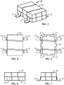
- FIG. 3 is a perspective view, left top of one embodiment of a surface-mountable semiconductor device 30.
- FIGs. 4-7 respectively show a top view, bottom view, left front view (right view mirror), and a front view (back view mirror) of the semiconductor device. 30.
- the device 30 includes a semiconductor die (not visible in FIGs. 3-7 ) such as a diode, a MOSFET, or another type of die/integrated circuit, for example.
- the die is contained within a housing 40.
- Electrically conductive attachment regions 32 e.g., lead frames
- Most surfaces of the housing 40 are formed of a material such as a molding compound. However, as shown in FIG.
- At least a portion of one surface of the housing 40 is formed from a metallic plate 45 that serves as a heat sink.
- the metallic plate 45 is located on the bottom surface of the device 30.
- the bottom surface of the housing 40 also includes a peripheral lip or edge 47 formed from the same material (e.g., a molding compound) as the remainder of the housing. The peripheral edge 47 largely surrounds the metallic plate 45 and is coplanar therewith.
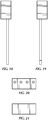
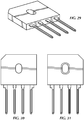
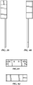
- FIGs. 3-56 Various views of alternative embodiments are depicted in FIGs. 3-56 .
- the semiconductor device 30 may be fabricated in accordance with a wide variety of different techniques and materials.
- the device 30 may also have a wide variety of different internal configurations. The following examples will present one such configuration constructed in accordance with one particular technique, which is presented by way of example only and not as a limitation on the invention.
- FIG. 57 is a side view of an interior cross-section of a through-hole mountable semiconductor device 200.
- Electrically conductive attachment regions 202 such as copper pads, solder balls, leads, lead frames, or lead frame terminals, each have one surface 203 arranged to provide electrical communication with a semiconductor die 206 (three dies are visible, although only one die is referenced for exemplary purposes.)
- Die 206 may be, for example, a diode, a MOSFET, or another type of die/integrated circuit.
- Surface 203 may be attached to die 206 in any suitable manner, such as by soldering.
- Through-hole mountable leads 212 (one visible) may also be in electrical communication with semiconductor die 206 and/or electrically conductive attachment region 202.
- a housing 210 at least in part encloses die 206 and electrically conductive attachment regions 202.
- Housing 210 is a molding compound, such as a plastic, molded to thermally conductive element 202 and interlayer material 208.
- Housing 210 may be formed in any desired configuration/shape by a variety of well-known methods, such as overmolding or injection molding. As shown, housing 210 is approximately 3.5 mm thick with a configuration similar to portions of exterior housing 12 of semiconductor device 10 (shown in FIG. 1 ). However, the portion 230 of the housing 210 located between electrically conductive attachment regions 202 and interlayer material 208 (discussed below) is reduced in thickness. That is, the thickness of the housing 210 on the side 205 of the electrically conductive attachment region 202 is substantially thinner than the thickness of the housing 210 on the side 203 of the electrically conductive attachment region 202 on which the die 206 is located.
- an interlayer material 208 is coated or otherwise applied to the exposed surface of the housing portion 230 (i.e., the portion of housing 210 on the side 205 of the electrically conductive attachment region 202).
- the interlayer material 208 has a high dielectric constant and a high thermal conductivity.
- the interlayer material 208 may take the form of a thermally conductive silicone elastomer material, grease, epoxy, elastomeric pad, thermal tape, fluid, or gel.
- the interlayer material 208 may be a commercially available thermally conductive adhesive such as - SE4486 and SE4450 manufactured by DOW CORNING, 282 manufactured by Emerson&Cuming, and SA2000 manufactured by BERGQUIST.
- a metal heat sink such as metal plate 220 is secured to the interlayer material 208.
- the metal plate 220 may be secured by any appropriate means.
- the interlayer material 208 is formed from an adhesive, the interlayer material 208 itself may serve to secure the metal plate 220.
- the semiconductor device shown in FIG. 57 accommodates both a heat sink and a thinner housing wall, thereby increasing the thermal dissipation of the device so that the device can carry higher currents.
- FIGs. 58-61 show cross-sectional views of the through-hole mountable semiconductor device shown in FIG. 57 during the fabrication process.
- FIG. 58 shows the die 206 mounted to the upper surface of the electrically conductive attachment region 202.
- the housing 210 is formed in an overmolding processes. Housing 210 includes an upper portion that surrounds die 206 and a lower portion 230 that contacts the side 205 of the electrically conductive attachment region 202.
- a recess 240 is formed in housing portion 230 that will accommodate both the interlayer material 208 and the metal plate 220.
- FIG. 60 shows for illustrative purpose only an embodiment not falling under the invention wherein an interlayer material 208 is located in the recess 240 and FIG.
- the 61 shows the metal plate 220 inserted in the recess 240 and in contact with the interlayer material 208.
- the interlayer material 208 is first applied to the metal plate 220 before inserting the metal plate 220 into the recess 240. Also, as previously mentioned, the interlayer material 208 serves as an adhesive that secures the metal plate 220 in the recess 240.
- the thickness d of the housing extending from the surface of the electrically conductive attachment region 202 can be advantageously reduced while still avoiding deleterious effects caused to the semiconductor device 200 by IPE (Internal Parts Exposure) or voids.
- the housing thickness d can be reduced by 50% or more.
- the housing thickness d may be reduced from 1.0 mm to 0.5 mm in thickness.
- the semiconductor device 200 can avoid hipot test failures even with such a reduction in housing thickness.
- the interlayer material 208 effectively acts as a shield providing a high dielectric strength during a hipot test while also allowing good thermal conduction because of its high thermal conductivity.
- the interlayer material 208 is coated or applied to the electrically conductive attachment region 202 using a screen printing process.
- Screen printing techniques have been widely used in the graphic arts fields to produce art work and have found use in the production of printed circuit boards to transfer relatively large scale mask patterns onto printed circuit boards.
- Screen printing techniques include the use of a stencil to selectively transfer an image onto a substrate. The image is typically transferred by mechanically pressing a given material through porous (e.g., mesh) portions of the stencil onto a substrate while adjacent non-porous portions of the stencil do not permit printing of the material.
- Screen printed materials of use in the production of graphic art work include paints and/or inks, while materials of use in the transfer of mask patterns in circuit board production include masking materials.
- Stencils for use in screen printing are often created by laser milling an image onto a stencil or by photo development processes wherein an image is photo transferred to an undeveloped stencil and the stencil is subsequently developed to reveal the image.
- An undeveloped stencil typically includes a screen that is coated with a non-porous material. Upon development, portions of the non-porous material are removed yielding porous section of the stencil or yielding apertures in the stencil in the configuration of a photo transferred image. As the image is in effect transferred to the developed stencil, the stencil is then of use to transfer the same image to a substrate as discussed above.
- the techniques of screen printing and the use of stencils in such printing are well known and therefore, will not be discussed in any greater detail.
- semiconductor devices have been described that include enhanced heat removal paths created by reducing the thickness of the housing that encapsulates the die or dies as well as by providing a metal heat sink.
- Conducting heat away from mounting substrates is desirable in product designs that feature increased component densities, and thus increased heat flux densities, on each substrate--cooling provided for the substrate, which generally results in a single operating temperature being provided for a relatively large surface area, is supplemented by the electrically isolated semiconductor device package itself.
- Semiconductor devices may operate at more desirable temperatures without significant alterations in their footprints, and/or without additional isolation requirements, reducing the need for product re-designs.
- FIG. 62 is a flowchart of a method for manufacturing a semiconductor device such as the semiconductor device 200 shown in FIG. 57 for illustrative purpose only, not falling under the invention.
- the method begins at block 902, where a semiconductor die is arranged for electrical communication with a first attachment area of an electrically conductive attachment region, such as a copper pad, a lead frame, or a terminal thereof.
- a thermally conductive, dielectric interlayer material is applied to a metal plate that serves as a heat sink.
- the interlayer material is coated onto the metal plate and serves as an adhesive.
- the metal plate is attached to the second attachment area of the electrically conductive attachment region so that the interlayer material contacts the second attachment area. If the interlayer material is an adhesive, it may serve to secure the metal plate to the second attachment area.
- a housing which may be composed of a material such as plastic, is provided that at least in part encloses the die, the interlayer material, the metal plate and the electrically conductive attachment region.
- the housing is affixed (by molding, for example) in such a manner that exterior packaging of the semiconductor device is provided by the housing.
- the thickness of the housing extending from the electrically conductive attachment region may be less than would otherwise be possible while still avoiding problems (e.g. electrical insulation breakdowns) caused by voids and the like if the interlayer material and the metal plate were not employed.
Landscapes
- Structures Or Materials For Encapsulating Or Coating Semiconductor Devices Or Solid State Devices (AREA)
- Cooling Or The Like Of Semiconductors Or Solid State Devices (AREA)
- Lead Frames For Integrated Circuits (AREA)
Description
- Aspects of this invention relate generally to a semiconductor device, and more particularly to a semiconductor device encapsulated in a housing that includes a metallic plate.
-
JP H06-5737 A -
JP S58-100447 A -
JP H05-144983 A - A major cause of reduced efficiency in semiconductor devices such as rectifiers is inadequate cooling during normal operation. Two ways to alleviate this problem involve the use of a heat sink and a reduction in the wall thickness of the housing that encapsulates the semiconductor device.
-
FIG. 1a and 1b are perspective and side views, respectively, of a Vishay® Semiconductor brand single phase inlinebridge rectifier device 10 having four semiconductor die inside (not shown), manufactured by Vishay Intertechnology, Inc.Device 10 is through-hole mountable vialeads 14, and includes anexterior epoxy housing 12 that protects the semiconductor dies-- during operation ofdevice 10, heat generated by the semiconductor dies is transferred throughleads 14 andhousing 12. FIG. IB is a side view ofdevice 10, illustrating the through-hole mounting thereof to a substrate 11 (a circuit board, for example), and further illustrating how a heat sink (such as a finned aluminum plate) 13 may be used to increase the thermal dissipation performance ofhousing 12--heat generated by dies withinhousing 12 is transferred tosubstrate 11 vialeads 14, and throughhousing 12 to heatsink 13 and/or the ambient environment.Device 10,substrate 11, andheat sink 13 are cooled using a cooling technique such as natural or forced-air convection. The thermal conductivity ofepoxy housing 12 is much less than that ofheat sink 13, however, which often results indevice 10 having poor thermal dissipation performance. Unfortunately, thehousing 12 is necessary to protect the semiconductor device against moisture as well as assembly process and other environmental contaminants. Thehousing 12 is commonly formed by encapsulating the semiconductor device in a mold compound, such as a thermosetting plastic, applied by a transfer molding process. - In a typical transfer molding machine used in the semiconductors industry, a thin electronic workpiece mounted on a lead frame is clamped between two halves of a split mold. The mold defines a mold cavity around the device with sufficient clearance to allow mold compound to be injected and flow around the device to encapsulate it. During the molding process mold compound is injected into an inlet and air inside the mold escapes from a vent. A plunger drives the liquefied mold compound into the mold cavity. The mold compound is allowed cure and the mold is opened, releasing the encapsulated semiconductor device.
- As previously mentioned, to increase heat dissipation device manufacturers would like to reduce the thickness of the encapsulating layer of the mold compound which encases each device. Thinner encapsulating layers also aid in improving device performance or reliability with regard, resistance to coating damage under thermal stress and other parameters. Another reason thinner encapsulating layers are desired is that in general smaller semiconductor devices are preferred over larger device. However, as the distance between the inner mold surfaces and the electronic workpiece is decreased, it becomes more difficult to obtain a high quality void-free encapsulant around the entire device.
- To obtain a void-free seal, the liquefied mold compound must enter the mold inlet and entirely fill the space in the mold cavity before the mold compound flow front arrives at the mold vent. If the mold compound reaches the vent before the mold is completely filled, an air bubble is trapped in the mold, creating a void.
- To completely fill the mold cavity, the mold compound must flow between the upper mold surface and the upper surface of the device, between the lower mold surface and the lower surface of the device, and into the space surrounding the outer perimeter of the device. However, as the distance between the upper and lower mold surfaces and the device is reduced, so as to make the encapsulating coating thinner, it becomes more difficult for the mold compound to penetrate these regions.
- If this distance is reduced too far, the mold compound will flow around the outer perimeter of the device before the mold compound flow front has displaced the air in the space above and below the device. The result is a void in the encapsulation material as an air bubble is pinched off in the center of the device.
- As a result, transfer molding of semiconductor devices with conventional equipment has required that the distance from the inner mold surfaces to the device be at least about 200-250 micrometers. This ensures that there will be laminar flow of the molding compound into the mold and around the device. The exact minimum distance limit is, of course, a function of the specific mold compound used, the fillers it contains and process parameters, such as temperature, but, in general, reducing the distance from the inner mold surfaces to the device to less than some minimum distance results in unacceptable manufacturing losses due to the formation of voids.
-
FIG. 2 is a cross-sectional view of asemiconductor device 10 such as depicted inFIGs. 1a and 1b . Similar to the device inFIG. 1 ,device 10 is through-hole mountable vialeads 112, and includes anexterior epoxy housing 110 that protects the semiconductor dies 106-- during operation ofdevice 10, heat generated by thesemiconductor dies 106 is transferred throughleads 112 andhousing 110. The thermal conductivity ofepoxy housing 110 often results indevice 10 having poor thermal dissipation performance. A major cause of reduced efficiency in semiconductor devices such as rectifiers is inadequate cooling during normal operation. Unfortunately, as discussed above, if the thickness of the housing is reduced to achieve better thermal conduction, molding failures such as IPE or voids 130 (seeFIG. 2 ) tend to increase, leading to problems such as a failure of a high-potential (hipot) test or electric strength test, which is caused by a breakdown in insulation. - Accordingly, it would be desirable to accommodate both a heat sink and a thinner housing wall in order to adequately dissipate heat in a semiconductor device such as a bridge rectifier.
- In accordance with the present invention, a semiconductor device mountable to a substrate as defined in Claim 1 is provided. The device includes a semiconductor die and an electrically conductive lead frame having first and second end portions and a first attachment surface and a second attachment surface. The die electrically contacts the first end portion of the lead frame on the first attachment surface. An externally exposed housing encloses the semiconductor die and the first end portion of the lead frame, said housing including a metallic plate facing the second attachment surface of the lead frame.
- In accordance with one aspect of the invention, the semiconductor device comprises a power semiconductor device.
- In accordance with another aspect of the invention, the power semiconductor device comprises a rectifier. the rectifier comprises a bridge rectifier.
- In accordance with another aspect of the invention, the semiconductor device comprises a surface-mountable device.
- In accordance with another aspect of the invention, the semiconductor device comprises a through-hole-mountable device.
- In accordance with another aspect of the invention, the semiconductor device comprises an integrated circuit.
- In accordance with another aspect of the invention, the integrated circuit comprises a chip-scale package.
-
-
FIGs. 1a and 1b are perspective and side views, respectively, of the packaging for a conventional through-hole mountable semiconductor device. -
FIG. 2 is a cross-sectional view of the packaging for a conventional through-hole mountable semiconductor device. -
FIG. 3 is a perspective view, left top of one illustrative embodiment of a semiconductor device, not falling under the invention; -
FIG. 4 is a top view thereof; -
FIG. 5 is a bottom view thereof; -
FIG. 6 is a left of front view (right view mirror) thereof; and -
FIG. 7 is a front view (back view mirror) thereof. -
FIG. 8 is a perspective view, left top of another illustrative embodiment of a semiconductor device, not falling under the invention; -
FIG. 9 is a top view thereof; -
FIG. 10 is a bottom view thereof; -
FIG. 11 is a left of front view thereof; -
FIG. 12 is a right of front view thereof; -
FIG. 13 is a front view thereof; and -
FIG. 14 is a back view thereof. -
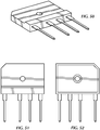
FIG. 15 is a perspective view, left top of another embodiment of a semiconductor device; -
FIG. 16 is a top view thereof; -
FIG. 17 is a bottom view thereof; -
FIG. 18 is a left of front view thereof; -
FIG. 19 is a right of front view thereof; -
FIG. 20 is a front view thereof; and -
FIG. 21 is a back view thereof. -
FIG. 22 is a perspective view, left top of another embodiment of a semiconductor device; -
FIG. 23 is a top view thereof; -
FIG. 24 is a bottom view thereof; -
FIG. 25 is a left of front view thereof; -
FIG. 26 is a right of front view thereof; -
FIG. 27 is a front view thereof; and -
FIG. 28 is a back view thereof. -
FIG. 29 is a perspective view, left top of another embodiment of a semiconductor device; -
FIG. 30 is a top view thereof; -
FIG. 31 is a bottom view thereof; -
FIG. 32 is a left of front view thereof; -
FIG. 33 is a right of front view thereof; -
FIG. 34 is a front view thereof; and -
FIG. 35 is a back view thereof. -
FIG. 36 is a perspective view, left top of another embodiment of a semiconductor device; -
FIG. 37 is a top view thereof; -
FIG. 38 is a bottom view thereof; -
FIG. 39 is a left of front view thereof; -
FIG. 40 is a right of front view thereof; -
FIG. 41 is a front view thereof; and -
FIG. 42 is a back view thereof. -
FIG. 43 is a perspective view, left top of another embodiment of a semiconductor device; -
FIG. 44 is a top view thereof; -
FIG. 45 is a bottom view thereof; -
FIG. 46 is a left of front view thereof; -
FIG. 47 is a right of front view thereof; -
FIG. 48 is a front view thereof; and -
FIG. 49 is a back view thereof. -
FIG. 50 is a perspective view, left top of another embodiment of a semiconductor device; -
FIG. 51 is a top view thereof; -
FIG. 52 is a bottom view thereof; -
FIG. 53 is a left of front view thereof; -
FIG. 54 is a right of front view thereof; -
FIG. 55 is a front view thereof; and -
FIG. 56 is a back view thereof. -
FIG. 57 is a cross-sectional view of the packaging for a through-hole mountable semiconductor device constructed in accordance one aspect of the present invention. -
FIGs. 58-61 show cross-sectional views of the through-hole mountable semiconductor device shown inFIG. 3 during the fabrication process. -
FIG. 62 is a flowchart of a method for fabricating a semiconductor device, not falling under the invention. -
FIG. 3 is a perspective view, left top of one embodiment of a surface-mountable semiconductor device 30. In addition,FIGs. 4-7 respectively show a top view, bottom view, left front view (right view mirror), and a front view (back view mirror) of the semiconductor device. 30. Thedevice 30 includes a semiconductor die (not visible inFIGs. 3-7 ) such as a diode, a MOSFET, or another type of die/integrated circuit, for example. The die is contained within ahousing 40. Electrically conductive attachment regions 32 (e.g., lead frames), which electrically contact the die, extend through thehousing 40 so that they are externally accessible. Most surfaces of thehousing 40 are formed of a material such as a molding compound. However, as shown inFIG. 5 , at least a portion of one surface of thehousing 40 is formed from ametallic plate 45 that serves as a heat sink. In this embodiment themetallic plate 45 is located on the bottom surface of thedevice 30. In addition, in this embodiment the bottom surface of thehousing 40 also includes a peripheral lip or edge 47 formed from the same material (e.g., a molding compound) as the remainder of the housing. Theperipheral edge 47 largely surrounds themetallic plate 45 and is coplanar therewith. - Various views of alternative embodiments are depicted in
FIGs. 3-56 . - The
semiconductor device 30 may be fabricated in accordance with a wide variety of different techniques and materials. Thedevice 30 may also have a wide variety of different internal configurations. The following examples will present one such configuration constructed in accordance with one particular technique, which is presented by way of example only and not as a limitation on the invention. -
FIG. 57 is a side view of an interior cross-section of a through-holemountable semiconductor device 200. Electricallyconductive attachment regions 202, such as copper pads, solder balls, leads, lead frames, or lead frame terminals, each have onesurface 203 arranged to provide electrical communication with a semiconductor die 206 (three dies are visible, although only one die is referenced for exemplary purposes.)Die 206 may be, for example, a diode, a MOSFET, or another type of die/integrated circuit.Surface 203 may be attached to die 206 in any suitable manner, such as by soldering. Through-hole mountable leads 212 (one visible) may also be in electrical communication with semiconductor die 206 and/or electricallyconductive attachment region 202. - A
housing 210 at least in part encloses die 206 and electricallyconductive attachment regions 202.Housing 210 is a molding compound, such as a plastic, molded to thermallyconductive element 202 andinterlayer material 208.Housing 210 may be formed in any desired configuration/shape by a variety of well-known methods, such as overmolding or injection molding. As shown,housing 210 is approximately 3.5 mm thick with a configuration similar to portions ofexterior housing 12 of semiconductor device 10 (shown inFIG. 1 ). However, theportion 230 of thehousing 210 located between electricallyconductive attachment regions 202 and interlayer material 208 (discussed below) is reduced in thickness. That is, the thickness of thehousing 210 on theside 205 of the electricallyconductive attachment region 202 is substantially thinner than the thickness of thehousing 210 on theside 203 of the electricallyconductive attachment region 202 on which thedie 206 is located. - As further shown in
FIG. 57 , aninterlayer material 208 is coated or otherwise applied to the exposed surface of the housing portion 230 (i.e., the portion ofhousing 210 on theside 205 of the electrically conductive attachment region 202). Theinterlayer material 208 has a high dielectric constant and a high thermal conductivity. Theinterlayer material 208 may take the form of a thermally conductive silicone elastomer material, grease, epoxy, elastomeric pad, thermal tape, fluid, or gel. For instance, theinterlayer material 208 may be a commercially available thermally conductive adhesive such as - SE4486 and SE4450 manufactured by DOW CORNING, 282 manufactured by Emerson&Cuming, and SA2000 manufactured by BERGQUIST. Finally, a metal heat sink such asmetal plate 220 is secured to theinterlayer material 208. Themetal plate 220 may be secured by any appropriate means. For example, if theinterlayer material 208 is formed from an adhesive, theinterlayer material 208 itself may serve to secure themetal plate 220. Thus, the semiconductor device shown inFIG. 57 accommodates both a heat sink and a thinner housing wall, thereby increasing the thermal dissipation of the device so that the device can carry higher currents. -
FIGs. 58-61 show cross-sectional views of the through-hole mountable semiconductor device shown inFIG. 57 during the fabrication process.FIG. 58 shows thedie 206 mounted to the upper surface of the electricallyconductive attachment region 202. InFIG. 59 thehousing 210 is formed in an overmolding processes.Housing 210 includes an upper portion that surrounds die 206 and alower portion 230 that contacts theside 205 of the electricallyconductive attachment region 202. Arecess 240 is formed inhousing portion 230 that will accommodate both theinterlayer material 208 and themetal plate 220.FIG. 60 shows for illustrative purpose only an embodiment not falling under the invention wherein aninterlayer material 208 is located in therecess 240 andFIG. 61 shows themetal plate 220 inserted in therecess 240 and in contact with theinterlayer material 208. Theinterlayer material 208 is first applied to themetal plate 220 before inserting themetal plate 220 into therecess 240. Also, as previously mentioned, theinterlayer material 208 serves as an adhesive that secures themetal plate 220 in therecess 240. - By using
interlayer material 208 the thickness d of the housing extending from the surface of the electrically conductive attachment region 202 (seeFIG. 57 ) can be advantageously reduced while still avoiding deleterious effects caused to thesemiconductor device 200 by IPE (Internal Parts Exposure) or voids. In some cases the housing thickness d can be reduced by 50% or more. For instance, the housing thickness d may be reduced from 1.0 mm to 0.5 mm in thickness. In particular, thesemiconductor device 200 can avoid hipot test failures even with such a reduction in housing thickness. Theinterlayer material 208 effectively acts as a shield providing a high dielectric strength during a hipot test while also allowing good thermal conduction because of its high thermal conductivity. - The
interlayer material 208 is coated or applied to the electricallyconductive attachment region 202 using a screen printing process. Screen printing techniques have been widely used in the graphic arts fields to produce art work and have found use in the production of printed circuit boards to transfer relatively large scale mask patterns onto printed circuit boards. Screen printing techniques include the use of a stencil to selectively transfer an image onto a substrate. The image is typically transferred by mechanically pressing a given material through porous (e.g., mesh) portions of the stencil onto a substrate while adjacent non-porous portions of the stencil do not permit printing of the material. Screen printed materials of use in the production of graphic art work include paints and/or inks, while materials of use in the transfer of mask patterns in circuit board production include masking materials. Stencils for use in screen printing are often created by laser milling an image onto a stencil or by photo development processes wherein an image is photo transferred to an undeveloped stencil and the stencil is subsequently developed to reveal the image. An undeveloped stencil typically includes a screen that is coated with a non-porous material. Upon development, portions of the non-porous material are removed yielding porous section of the stencil or yielding apertures in the stencil in the configuration of a photo transferred image. As the image is in effect transferred to the developed stencil, the stencil is then of use to transfer the same image to a substrate as discussed above. The techniques of screen printing and the use of stencils in such printing are well known and therefore, will not be discussed in any greater detail. - Thus semiconductor devices have been described that include enhanced heat removal paths created by reducing the thickness of the housing that encapsulates the die or dies as well as by providing a metal heat sink.. Conducting heat away from mounting substrates is desirable in product designs that feature increased component densities, and thus increased heat flux densities, on each substrate--cooling provided for the substrate, which generally results in a single operating temperature being provided for a relatively large surface area, is supplemented by the electrically isolated semiconductor device package itself. Semiconductor devices may operate at more desirable temperatures without significant alterations in their footprints, and/or without additional isolation requirements, reducing the need for product re-designs.
- Aspects of the present invention described above with respect to a through-hole mountable semiconductor devices are also applicable to surface-mountable semiconductor devices, such as shown, for example, in
FIG. 8 ofUS 2008/0036072 A1 . -
FIG. 62 is a flowchart of a method for manufacturing a semiconductor device such as thesemiconductor device 200 shown inFIG. 57 for illustrative purpose only, not falling under the invention. The method begins atblock 902, where a semiconductor die is arranged for electrical communication with a first attachment area of an electrically conductive attachment region, such as a copper pad, a lead frame, or a terminal thereof. - Next, at
block 904, a thermally conductive, dielectric interlayer material is applied to a metal plate that serves as a heat sink. The interlayer material is coated onto the metal plate and serves as an adhesive. Atstep 906 the metal plate is attached to the second attachment area of the electrically conductive attachment region so that the interlayer material contacts the second attachment area. If the interlayer material is an adhesive, it may serve to secure the metal plate to the second attachment area. - At
block 908, a housing, which may be composed of a material such as plastic, is
provided that at least in part encloses the die, the interlayer material, the metal plate and the electrically conductive attachment region. The housing is affixed (by molding, for example) in such a manner that exterior packaging of the semiconductor device is provided by the housing. The thickness of the housing extending from the electrically conductive attachment region may be less than would otherwise be possible while still avoiding problems (e.g. electrical insulation breakdowns) caused by voids and the like if the interlayer material and the metal plate were not employed.
Claims (8)
- A semiconductor device (30, 200) mountable to a substrate, comprising:- a plurality of semiconductor dies (206);- an electrically conductive continuous lead frame 202) having a first end portion to be enclosed by a housing and a second end portion and a first attachment surface (203) and a second attachment surface (205), wherein the semiconductor dies (206) electrically and mechanically contact the first end portion of the lead frame (202) on the first attachment surface (203), the first end portion and the second end portion being continuously connected to one another, and wherein each of the semiconductor dies (206) and the lead frame (202) are collinear with one another;- an externally exposed housing (40, 210) enclosing the semiconductor dies (206) and the first end portion of the lead frame (202), said housing (40, 210) including a metallic plate (45, 220) facing the second attachment surface (205) of the lead frame (202); and- a dielectric, thermally conductive interlayer material (208) screen printed as a coating on the metallic plate (45, 220), wherein the interlayer material (208) is disposed between the metallic plate (45, 220) and the second attachment surface (205) of the lead frame (202), wherein the metallic plate (45, 220) is secured using the interlayer material (208) as an adhesive;wherein a portion (230) of said housing (40, 210) lies between said second attachment surface (205) of the lead frame (202) and the metallic plate (45, 220), wherein the lead frame (202) extends through said housing (40, 210), so that it is externally accessible, wherein said housing (40, 210) is a molding compound (40, 210), wherein a thickness of any portion of said housing (210) located directly over the interlayer material (208) on the side of the second attachment surface (205) and between the electrically conductive lead frame (202) and the interlayer material (208) is thinner than a thickness of said housing (210) located on the side of the first attachment surface (203), and wherein a portion of the molding compound (210) is coplanar with the metallic plate (220) and surrounds the metallic plate (220).
- The semiconductor device (200) according to claim 1, wherein the semiconductor device (200) comprises a power semiconductor device.
- The semiconductor device (200) according to claim 2, wherein the power semiconductor device comprises a rectifier.
- The semiconductor device (200) according to claim 3, wherein the rectifier comprises a bridge rectifier.
- The semiconductor device (200) according to claim 1, wherein the semiconductor device (200) comprises a surface-mountable device.
- The semiconductor device (200) according to claim 1, wherein the semiconductor device (200) comprises a through-hole-mountable device.
- The semiconductor device (200) according to claim 1, wherein the semiconductor device (200) comprises an integrated circuit (206).
- The semiconductor device (200) according to claim 7, wherein the integrated circuit (206) comprises a chip-scale package.
Applications Claiming Priority (5)
| Application Number | Priority Date | Filing Date | Title |
|---|---|---|---|
| US83683506P | 2006-08-10 | 2006-08-10 | |
| US83735306P | 2006-08-11 | 2006-08-11 | |
| US11/827,042 US8048714B2 (en) | 2006-08-11 | 2007-07-09 | Semiconductor device and method for manufacturing a semiconductor device having improved heat dissipation capabilities |
| US11/836,579 US8269338B2 (en) | 2006-08-10 | 2007-08-09 | Semiconductor device having improved heat dissipation capabilities |
| PCT/US2007/017767 WO2008021219A2 (en) | 2006-08-10 | 2007-08-10 | Semiconductor device having improved heat dissipation capabilities |
Publications (3)
| Publication Number | Publication Date |
|---|---|
| EP2057679A2 EP2057679A2 (en) | 2009-05-13 |
| EP2057679A4 EP2057679A4 (en) | 2012-08-01 |
| EP2057679B1 true EP2057679B1 (en) | 2020-01-01 |
Family
ID=39082624
Family Applications (1)
| Application Number | Title | Priority Date | Filing Date |
|---|---|---|---|
| EP07811243.0A Active EP2057679B1 (en) | 2006-08-10 | 2007-08-10 | Semiconductor device having improved heat dissipation capabilities |
Country Status (5)
| Country | Link |
|---|---|
| US (1) | US8269338B2 (en) |
| EP (1) | EP2057679B1 (en) |
| JP (1) | JP2010500754A (en) |
| TW (1) | TWI415233B (en) |
| WO (1) | WO2008021219A2 (en) |
Families Citing this family (8)
| Publication number | Priority date | Publication date | Assignee | Title |
|---|---|---|---|---|
| US8093713B2 (en) * | 2007-02-09 | 2012-01-10 | Infineon Technologies Ag | Module with silicon-based layer |
| JP5714916B2 (en) * | 2011-01-12 | 2015-05-07 | ルネサスエレクトロニクス株式会社 | Semiconductor device and manufacturing method thereof |
| WO2012108011A1 (en) * | 2011-02-09 | 2012-08-16 | 三菱電機株式会社 | Power semiconductor module |
| JP2013070026A (en) * | 2011-09-08 | 2013-04-18 | Rohm Co Ltd | Semiconductor device, manufacturing method of semiconductor device, mounting structure of semiconductor device, and power semiconductor device |
| CN106783764A (en) * | 2017-01-25 | 2017-05-31 | 长电科技(宿迁)有限公司 | A kind of fixed thimble interior insulation encapsulating structure and its process |
| CN106601714A (en) * | 2017-01-25 | 2017-04-26 | 长电科技(宿迁)有限公司 | A movable thimble inner insulation packaging structure and its process method |
| CN109996359A (en) * | 2019-03-29 | 2019-07-09 | 如皋市大昌电子有限公司 | A kind of bridge heap tooling preheating device |
| JP7406314B2 (en) * | 2019-06-24 | 2023-12-27 | キヤノン株式会社 | electronic modules and equipment |
Citations (1)
| Publication number | Priority date | Publication date | Assignee | Title |
|---|---|---|---|---|
| JPH05144983A (en) * | 1991-11-22 | 1993-06-11 | Mitsubishi Electric Corp | Resin-sealed semiconductor device |
Family Cites Families (32)
| Publication number | Priority date | Publication date | Assignee | Title |
|---|---|---|---|---|
| JPS54162470A (en) | 1978-06-13 | 1979-12-24 | Nec Corp | Resin sealing type semiconductor device |
| JPS58100447A (en) * | 1981-12-11 | 1983-06-15 | Hitachi Ltd | Resin sealing type semiconductor device and manufacture thereof |
| JPS61150354A (en) | 1984-12-25 | 1986-07-09 | Toshiba Corp | Resin sealed type semiconductor device |
| JPS63107159A (en) * | 1986-10-24 | 1988-05-12 | Toshiba Corp | Semiconductor device |
| JPH03191553A (en) * | 1989-12-20 | 1991-08-21 | Hitachi Ltd | Semiconductor device and manufacture thereof |
| US5216283A (en) * | 1990-05-03 | 1993-06-01 | Motorola, Inc. | Semiconductor device having an insertable heat sink and method for mounting the same |
| EP0521405B1 (en) * | 1991-07-01 | 2001-04-18 | Sumitomo Electric Industries, Ltd. | Heat radiating component and semiconductor device provided with the same |
| JPH05206365A (en) * | 1992-01-30 | 1993-08-13 | Fuji Electric Co Ltd | Semiconductor device and its lead frame for assembling |
| TW214597B (en) * | 1992-02-26 | 1993-10-11 | Mitsubishi Electric Machine | |
| JP2518994B2 (en) | 1992-04-22 | 1996-07-31 | 富士通株式会社 | Semiconductor device |
| JPH05335444A (en) * | 1992-06-04 | 1993-12-17 | Nec Corp | Mold package |
| JP2939094B2 (en) * | 1993-08-24 | 1999-08-25 | シャープ株式会社 | Method for manufacturing power semiconductor device |
| EP0650193A3 (en) * | 1993-10-25 | 1996-07-31 | Toshiba Kk | Semiconductor device and method for its manufacture. |
| JPH07176664A (en) * | 1993-10-25 | 1995-07-14 | Toshiba Corp | Semiconductor device and manufacturing method thereof |
| US5691567A (en) * | 1995-09-19 | 1997-11-25 | National Semiconductor Corporation | Structure for attaching a lead frame to a heat spreader/heat slug structure |
| JP3516789B2 (en) * | 1995-11-15 | 2004-04-05 | 三菱電機株式会社 | Semiconductor power module |
| JP3345241B2 (en) * | 1995-11-30 | 2002-11-18 | 三菱電機株式会社 | Semiconductor device |
| JPH10135380A (en) * | 1996-10-31 | 1998-05-22 | Hitachi Ltd | Semiconductor device |
| US6130473A (en) * | 1998-04-02 | 2000-10-10 | National Semiconductor Corporation | Lead frame chip scale package |
| US6404065B1 (en) * | 1998-07-31 | 2002-06-11 | I-Xys Corporation | Electrically isolated power semiconductor package |
| KR100342589B1 (en) * | 1999-10-01 | 2002-07-04 | 김덕중 | Semiconductor power modules and methods for manufacturing the same |
| US6329714B1 (en) * | 1999-11-01 | 2001-12-11 | General Semiconductor, Inc. | Hybrid S.C. devices and method of manufacture thereof |
| JP3737673B2 (en) * | 2000-05-23 | 2006-01-18 | 株式会社ルネサステクノロジ | Semiconductor device |
| KR100370231B1 (en) * | 2000-06-13 | 2003-01-29 | 페어차일드코리아반도체 주식회사 | Power module package having a insulator type heat sink attached a backside of leadframe & manufacturing method thereof |
| US7061080B2 (en) * | 2001-06-11 | 2006-06-13 | Fairchild Korea Semiconductor Ltd. | Power module package having improved heat dissipating capability |
| KR100442847B1 (en) * | 2001-09-17 | 2004-08-02 | 페어차일드코리아반도체 주식회사 | Power semiconductor module that has three dimensional structure and a method of manufacturing thereof |
| JP2003124437A (en) * | 2001-10-19 | 2003-04-25 | Mitsubishi Electric Corp | Semiconductor device |
| KR100902766B1 (en) * | 2002-09-27 | 2009-06-15 | 페어차일드코리아반도체 주식회사 | Discrete Packages with Insulated Ceramic Heat Sink |
| US7292445B2 (en) * | 2003-02-25 | 2007-11-06 | Siliconix Technology C.V.-Ir | Active integrated rectifier regulator |
| US20060090855A1 (en) * | 2004-10-29 | 2006-05-04 | Tokyo Electron Limited | Substrate mounting table, substrate processing apparatus and substrate temperature control method |
| TW200642550A (en) * | 2005-05-25 | 2006-12-01 | Cyntec Co Ltd | Power module package structure |
| US8204453B2 (en) * | 2008-08-20 | 2012-06-19 | Intel Mobile Communications GmbH | Method, apparatus and communication unit |
-
2007
- 2007-08-09 US US11/836,579 patent/US8269338B2/en active Active
- 2007-08-10 JP JP2009523856A patent/JP2010500754A/en active Pending
- 2007-08-10 WO PCT/US2007/017767 patent/WO2008021219A2/en not_active Ceased
- 2007-08-10 TW TW096129700A patent/TWI415233B/en active
- 2007-08-10 EP EP07811243.0A patent/EP2057679B1/en active Active
Patent Citations (1)
| Publication number | Priority date | Publication date | Assignee | Title |
|---|---|---|---|---|
| JPH05144983A (en) * | 1991-11-22 | 1993-06-11 | Mitsubishi Electric Corp | Resin-sealed semiconductor device |
Also Published As
| Publication number | Publication date |
|---|---|
| US8269338B2 (en) | 2012-09-18 |
| TW200826262A (en) | 2008-06-16 |
| TWI415233B (en) | 2013-11-11 |
| US20080036057A1 (en) | 2008-02-14 |
| WO2008021219A3 (en) | 2008-11-20 |
| EP2057679A2 (en) | 2009-05-13 |
| WO2008021219A2 (en) | 2008-02-21 |
| EP2057679A4 (en) | 2012-08-01 |
| JP2010500754A (en) | 2010-01-07 |
Similar Documents
| Publication | Publication Date | Title |
|---|---|---|
| US6777819B2 (en) | Semiconductor package with flash-proof device | |
| US6429513B1 (en) | Active heat sink for cooling a semiconductor chip | |
| US8269338B2 (en) | Semiconductor device having improved heat dissipation capabilities | |
| US6130477A (en) | Thin enhanced TAB BGA package having improved heat dissipation | |
| US20030011054A1 (en) | Power module package having improved heat dissipating capability | |
| CN111937138B (en) | Semiconductor devices | |
| CN102468249A (en) | Power encapsulation module and method for manufacturing the power encapsulation module | |
| EP2057665B1 (en) | Semiconductor device and method for manufacturing a semiconductor device having improved heat dissipation capabilities | |
| US12068213B2 (en) | Chip package and semiconductor arrangement having thermally conductive material in contact with a semiconductor chip and methods of forming thereof | |
| EP2070113B1 (en) | Semiconductor device and method for manufacturing a semiconductor device | |
| CN101523596A (en) | Semiconductor device with improved heat dissipation | |
| US8865526B2 (en) | Semiconductor device and method for manufacturing a semiconductor device | |
| CN101496151A (en) | Semiconductor device and method of manufacturing semiconductor device | |
| JP7660708B2 (en) | Semiconductor power module and methods for manufacturing a semiconductor power module and a semiconductor power device | |
| KR101239117B1 (en) | Power semiconductor package and method for fabricating the same | |
| CN101595557A (en) | Semiconductor device and method for manufacturing semiconductor device with improved heat dissipation capability | |
| KR20150061441A (en) | Package Substrate and Manufacturing Method for the same and Power module Package using the same | |
| JPH07326690A (en) | Semiconductor device package and semiconductor device | |
| JPH0758246A (en) | Semiconductor device and manufacturing method thereof | |
| KR20020081906A (en) | Low profile optically-sensitive semiconductor package |
Legal Events
| Date | Code | Title | Description |
|---|---|---|---|
| PUAI | Public reference made under article 153(3) epc to a published international application that has entered the european phase |
Free format text: ORIGINAL CODE: 0009012 |
|
| AK | Designated contracting states |
Kind code of ref document: A2 Designated state(s): AT BE BG CH CY CZ DE DK EE ES FI FR GB GR HU IE IS IT LI LT LU LV MC MT NL PL PT RO SE SI SK TR |
|
| AX | Request for extension of the european patent |
Extension state: AL BA HR MK RS |
|
| 17P | Request for examination filed |
Effective date: 20090518 |
|
| RBV | Designated contracting states (corrected) |
Designated state(s): AT BE BG CH CY CZ DE DK EE ES FI FR GB GR HU IE IS IT LI LT LU LV MC MT NL PL PT RO SE SI SK TR |
|
| DAX | Request for extension of the european patent (deleted) | ||
| A4 | Supplementary search report drawn up and despatched |
Effective date: 20120704 |
|
| RIC1 | Information provided on ipc code assigned before grant |
Ipc: H01L 23/495 20060101AFI20120628BHEP Ipc: H01L 23/31 20060101ALI20120628BHEP Ipc: H01L 23/433 20060101ALI20120628BHEP |
|
| 17Q | First examination report despatched |
Effective date: 20140319 |
|
| STAA | Information on the status of an ep patent application or granted ep patent |
Free format text: STATUS: EXAMINATION IS IN PROGRESS |
|
| GRAP | Despatch of communication of intention to grant a patent |
Free format text: ORIGINAL CODE: EPIDOSNIGR1 |
|
| STAA | Information on the status of an ep patent application or granted ep patent |
Free format text: STATUS: GRANT OF PATENT IS INTENDED |
|
| INTG | Intention to grant announced |
Effective date: 20190809 |
|
| GRAS | Grant fee paid |
Free format text: ORIGINAL CODE: EPIDOSNIGR3 |
|
| GRAA | (expected) grant |
Free format text: ORIGINAL CODE: 0009210 |
|
| STAA | Information on the status of an ep patent application or granted ep patent |
Free format text: STATUS: THE PATENT HAS BEEN GRANTED |
|
| AK | Designated contracting states |
Kind code of ref document: B1 Designated state(s): AT BE BG CH CY CZ DE DK EE ES FI FR GB GR HU IE IS IT LI LT LU LV MC MT NL PL PT RO SE SI SK TR |
|
| REG | Reference to a national code |
Ref country code: GB Ref legal event code: FG4D |
|
| REG | Reference to a national code |
Ref country code: AT Ref legal event code: REF Ref document number: 1220866 Country of ref document: AT Kind code of ref document: T Effective date: 20200115 Ref country code: CH Ref legal event code: EP |
|
| REG | Reference to a national code |
Ref country code: DE Ref legal event code: R096 Ref document number: 602007059692 Country of ref document: DE |
|
| REG | Reference to a national code |
Ref country code: IE Ref legal event code: FG4D |
|
| REG | Reference to a national code |
Ref country code: CH Ref legal event code: NV Representative=s name: FREI PATENTANWALTSBUERO AG, CH |
|
| REG | Reference to a national code |
Ref country code: NL Ref legal event code: MP Effective date: 20200101 |
|
| REG | Reference to a national code |
Ref country code: LT Ref legal event code: MG4D |
|
| PG25 | Lapsed in a contracting state [announced via postgrant information from national office to epo] |
Ref country code: PT Free format text: LAPSE BECAUSE OF FAILURE TO SUBMIT A TRANSLATION OF THE DESCRIPTION OR TO PAY THE FEE WITHIN THE PRESCRIBED TIME-LIMIT Effective date: 20200527 Ref country code: FI Free format text: LAPSE BECAUSE OF FAILURE TO SUBMIT A TRANSLATION OF THE DESCRIPTION OR TO PAY THE FEE WITHIN THE PRESCRIBED TIME-LIMIT Effective date: 20200101 Ref country code: LT Free format text: LAPSE BECAUSE OF FAILURE TO SUBMIT A TRANSLATION OF THE DESCRIPTION OR TO PAY THE FEE WITHIN THE PRESCRIBED TIME-LIMIT Effective date: 20200101 Ref country code: NL Free format text: LAPSE BECAUSE OF FAILURE TO SUBMIT A TRANSLATION OF THE DESCRIPTION OR TO PAY THE FEE WITHIN THE PRESCRIBED TIME-LIMIT Effective date: 20200101 Ref country code: CZ Free format text: LAPSE BECAUSE OF FAILURE TO SUBMIT A TRANSLATION OF THE DESCRIPTION OR TO PAY THE FEE WITHIN THE PRESCRIBED TIME-LIMIT Effective date: 20200101 |
|
| PG25 | Lapsed in a contracting state [announced via postgrant information from national office to epo] |
Ref country code: GR Free format text: LAPSE BECAUSE OF FAILURE TO SUBMIT A TRANSLATION OF THE DESCRIPTION OR TO PAY THE FEE WITHIN THE PRESCRIBED TIME-LIMIT Effective date: 20200402 Ref country code: LV Free format text: LAPSE BECAUSE OF FAILURE TO SUBMIT A TRANSLATION OF THE DESCRIPTION OR TO PAY THE FEE WITHIN THE PRESCRIBED TIME-LIMIT Effective date: 20200101 Ref country code: SE Free format text: LAPSE BECAUSE OF FAILURE TO SUBMIT A TRANSLATION OF THE DESCRIPTION OR TO PAY THE FEE WITHIN THE PRESCRIBED TIME-LIMIT Effective date: 20200101 Ref country code: IS Free format text: LAPSE BECAUSE OF FAILURE TO SUBMIT A TRANSLATION OF THE DESCRIPTION OR TO PAY THE FEE WITHIN THE PRESCRIBED TIME-LIMIT Effective date: 20200501 Ref country code: BG Free format text: LAPSE BECAUSE OF FAILURE TO SUBMIT A TRANSLATION OF THE DESCRIPTION OR TO PAY THE FEE WITHIN THE PRESCRIBED TIME-LIMIT Effective date: 20200401 |
|
| REG | Reference to a national code |
Ref country code: DE Ref legal event code: R097 Ref document number: 602007059692 Country of ref document: DE |
|
| PG25 | Lapsed in a contracting state [announced via postgrant information from national office to epo] |
Ref country code: ES Free format text: LAPSE BECAUSE OF FAILURE TO SUBMIT A TRANSLATION OF THE DESCRIPTION OR TO PAY THE FEE WITHIN THE PRESCRIBED TIME-LIMIT Effective date: 20200101 Ref country code: RO Free format text: LAPSE BECAUSE OF FAILURE TO SUBMIT A TRANSLATION OF THE DESCRIPTION OR TO PAY THE FEE WITHIN THE PRESCRIBED TIME-LIMIT Effective date: 20200101 Ref country code: SK Free format text: LAPSE BECAUSE OF FAILURE TO SUBMIT A TRANSLATION OF THE DESCRIPTION OR TO PAY THE FEE WITHIN THE PRESCRIBED TIME-LIMIT Effective date: 20200101 Ref country code: EE Free format text: LAPSE BECAUSE OF FAILURE TO SUBMIT A TRANSLATION OF THE DESCRIPTION OR TO PAY THE FEE WITHIN THE PRESCRIBED TIME-LIMIT Effective date: 20200101 Ref country code: DK Free format text: LAPSE BECAUSE OF FAILURE TO SUBMIT A TRANSLATION OF THE DESCRIPTION OR TO PAY THE FEE WITHIN THE PRESCRIBED TIME-LIMIT Effective date: 20200101 |
|
| PLBE | No opposition filed within time limit |
Free format text: ORIGINAL CODE: 0009261 |
|
| STAA | Information on the status of an ep patent application or granted ep patent |
Free format text: STATUS: NO OPPOSITION FILED WITHIN TIME LIMIT |
|
| 26N | No opposition filed |
Effective date: 20201002 |
|
| PG25 | Lapsed in a contracting state [announced via postgrant information from national office to epo] |
Ref country code: PL Free format text: LAPSE BECAUSE OF FAILURE TO SUBMIT A TRANSLATION OF THE DESCRIPTION OR TO PAY THE FEE WITHIN THE PRESCRIBED TIME-LIMIT Effective date: 20200101 Ref country code: SI Free format text: LAPSE BECAUSE OF FAILURE TO SUBMIT A TRANSLATION OF THE DESCRIPTION OR TO PAY THE FEE WITHIN THE PRESCRIBED TIME-LIMIT Effective date: 20200101 |
|
| REG | Reference to a national code |
Ref country code: AT Ref legal event code: UEP Ref document number: 1220866 Country of ref document: AT Kind code of ref document: T Effective date: 20200101 |
|
| PG25 | Lapsed in a contracting state [announced via postgrant information from national office to epo] |
Ref country code: MC Free format text: LAPSE BECAUSE OF FAILURE TO SUBMIT A TRANSLATION OF THE DESCRIPTION OR TO PAY THE FEE WITHIN THE PRESCRIBED TIME-LIMIT Effective date: 20200101 |
|
| PG25 | Lapsed in a contracting state [announced via postgrant information from national office to epo] |
Ref country code: LU Free format text: LAPSE BECAUSE OF NON-PAYMENT OF DUE FEES Effective date: 20200810 |
|
| PG25 | Lapsed in a contracting state [announced via postgrant information from national office to epo] |
Ref country code: TR Free format text: LAPSE BECAUSE OF FAILURE TO SUBMIT A TRANSLATION OF THE DESCRIPTION OR TO PAY THE FEE WITHIN THE PRESCRIBED TIME-LIMIT Effective date: 20200101 Ref country code: MT Free format text: LAPSE BECAUSE OF FAILURE TO SUBMIT A TRANSLATION OF THE DESCRIPTION OR TO PAY THE FEE WITHIN THE PRESCRIBED TIME-LIMIT Effective date: 20200101 Ref country code: CY Free format text: LAPSE BECAUSE OF FAILURE TO SUBMIT A TRANSLATION OF THE DESCRIPTION OR TO PAY THE FEE WITHIN THE PRESCRIBED TIME-LIMIT Effective date: 20200101 |
|
| PGFP | Annual fee paid to national office [announced via postgrant information from national office to epo] |
Ref country code: DE Payment date: 20250722 Year of fee payment: 19 |
|
| PGFP | Annual fee paid to national office [announced via postgrant information from national office to epo] |
Ref country code: IT Payment date: 20250728 Year of fee payment: 19 |
|
| PGFP | Annual fee paid to national office [announced via postgrant information from national office to epo] |
Ref country code: BE Payment date: 20250724 Year of fee payment: 19 Ref country code: GB Payment date: 20250724 Year of fee payment: 19 |
|
| PGFP | Annual fee paid to national office [announced via postgrant information from national office to epo] |
Ref country code: AT Payment date: 20250725 Year of fee payment: 19 Ref country code: FR Payment date: 20250721 Year of fee payment: 19 |
|
| PGFP | Annual fee paid to national office [announced via postgrant information from national office to epo] |
Ref country code: CH Payment date: 20250901 Year of fee payment: 19 |
|
| PGFP | Annual fee paid to national office [announced via postgrant information from national office to epo] |
Ref country code: IE Payment date: 20250723 Year of fee payment: 19 |
|
| REG | Reference to a national code |
Ref country code: DE Ref legal event code: R079 Ref document number: 602007059692 Country of ref document: DE Free format text: PREVIOUS MAIN CLASS: H01L0023495000 Ipc: H10W0070400000 |