EP2055668A2 - Manufacturing method of an electronic device including overmoulded MEMS devices - Google Patents
Manufacturing method of an electronic device including overmoulded MEMS devices Download PDFInfo
- Publication number
- EP2055668A2 EP2055668A2 EP08018860A EP08018860A EP2055668A2 EP 2055668 A2 EP2055668 A2 EP 2055668A2 EP 08018860 A EP08018860 A EP 08018860A EP 08018860 A EP08018860 A EP 08018860A EP 2055668 A2 EP2055668 A2 EP 2055668A2
- Authority
- EP
- European Patent Office
- Prior art keywords
- resin layer
- membrane
- forming
- mems device
- opening
- Prior art date
- Legal status (The legal status is an assumption and is not a legal conclusion. Google has not performed a legal analysis and makes no representation as to the accuracy of the status listed.)
- Withdrawn
Links
Images




Classifications
-
- B—PERFORMING OPERATIONS; TRANSPORTING
- B81—MICROSTRUCTURAL TECHNOLOGY
- B81C—PROCESSES OR APPARATUS SPECIALLY ADAPTED FOR THE MANUFACTURE OR TREATMENT OF MICROSTRUCTURAL DEVICES OR SYSTEMS
- B81C1/00—Manufacture or treatment of devices or systems in or on a substrate
- B81C1/00015—Manufacture or treatment of devices or systems in or on a substrate for manufacturing microsystems
- B81C1/00261—Processes for packaging MEMS devices
- B81C1/00309—Processes for packaging MEMS devices suitable for fluid transfer from the MEMS out of the package or vice versa, e.g. transfer of liquid, gas, sound
-
- B—PERFORMING OPERATIONS; TRANSPORTING
- B81—MICROSTRUCTURAL TECHNOLOGY
- B81B—MICROSTRUCTURAL DEVICES OR SYSTEMS, e.g. MICROMECHANICAL DEVICES
- B81B2201/00—Specific applications of microelectromechanical systems
- B81B2201/02—Sensors
- B81B2201/0264—Pressure sensors
-
- B—PERFORMING OPERATIONS; TRANSPORTING
- B81—MICROSTRUCTURAL TECHNOLOGY
- B81B—MICROSTRUCTURAL DEVICES OR SYSTEMS, e.g. MICROMECHANICAL DEVICES
- B81B2201/00—Specific applications of microelectromechanical systems
- B81B2201/05—Microfluidics
- B81B2201/058—Microfluidics not provided for in B81B2201/051 - B81B2201/054
-
- B—PERFORMING OPERATIONS; TRANSPORTING
- B81—MICROSTRUCTURAL TECHNOLOGY
- B81C—PROCESSES OR APPARATUS SPECIALLY ADAPTED FOR THE MANUFACTURE OR TREATMENT OF MICROSTRUCTURAL DEVICES OR SYSTEMS
- B81C2203/00—Forming microstructural systems
- B81C2203/01—Packaging MEMS
- B81C2203/0154—Moulding a cap over the MEMS device
Definitions
- the present invention relates to a method for manufacturing an electronic device comprising overmoulded MEMS devices.
- the invention also relates to an electronic device comprising overmoulded MEMS devices.
- the invention particularly, but not exclusively, relates to a method for manufacturing an electronic device comprising MEMS sensors mounted on an LGA substrate, wherein the MEMS sensor needs a physical interface to communicate with the outside of the electronic device and the following description is made with reference to this field of application by way of illustration only.
- a MEMS device micro-electro-mechanical system
- a MEMS device is a miniaturised device or, in any case, a device having micrometric size which integrates mechanical and electrical functions in a chip or die of semiconductor material, for example of silicon, and which is realised by using micro-manufacturing lithographic techniques.
- the final assembled device is typically made of the silicon die wherein the MEMS device is integrated and, optionally, of integrated circuits for specific applications mounted on a substrate, for example of the LGA or BGA type (Land Grid Array or Ball Grid Array), flanked to or piled onto the MEMS device, by using conventional assembling processes.
- a cover or cap fixed to the substrate, overmoulds the MEMS device and the other devices mounted on the substrate, forming a casing which protects the MEMS device against external physical stresses.
- the cover is provided with a window to allow the interaction between the device and the outside of the assembled device.
- the substrate of the LGA/BGA type is formed by conductive layers insulated from each other by means of layers of insulating or dielectric material.
- the conductive layers are shaped in conductive tracks insulated from each other by layers of insulating or dielectric material.
- the MEMS devices are then electrically connected with the outside of the final device through wires connecting contact pads provided on the MEMS devices with conductive tracks present on the substrate inside the cover.
- a MEMS device in particular a pressure sensor, is realised on a substrate of the LGA type, to which it is glued, through a layer of epoxy glue.
- This sensor has a cavity above which there is a membrane and is connected to the substrate through metallic conductive wires. It is then covered by a closing wafer equipped with an opening in correspondence with the membrane of the sensor and through which the sensor is in communication with the outside. All the device is finally overmoulded in a casing.
- this solution shows different drawbacks.
- the complete device is made by first realising a casing bottom, then the different components are affixed to the casing bottom, and finally the casing is moulded and the element to control the sensor is inserted through the window of the casing.
- the procedure of alignment and positioning of the window to introduce the element for controlling the sensor is rather complicated, making the realisation of the device difficult to be reproduced.
- the manufacturing process of these devices is complicated by the presence of different assembling steps and relatively expensive.
- a second solution described in European patent no. EP 1 211 722, granted on September 8, 2004 to the same Applicant, provides the use of a casing which, by using a conventional technique, is equipped with a window in correspondence with an integrated electronic device, for example a sensor housed inside the casing and which must be put in communication with the outside of the casing.
- This window is obtained by using the same mould which is used to realise the casing; this mould is equipped with a protrusion projecting internally in correspondence with the sensor.
- a surface of the sensor is covered with a coating layer formed by material of the elastic type.
- the substrate is inserted in the mould so that the protrusion is in correspondence and in contact with the coating layer.
- the mould is then filled in by injection with an insulating material to realise, in a single step, the casing with window.
- the disadvantage of this solution consists in that the increase of the size of the holes made on the cap determines a weakening of the silicon slice which serves as cap, and a subsequent breakage of this one during the completion of the device.
- micro-channels A second method known for the formation of micro-channels is described in the US patent application publication No. 2006/0246416 . According to this method, the micro-channels are formed in the substrate of a first "chip”, called micro-porous "chip”, which is then glued to a second "chip”, called micro-fluidic "chip".
- micro-porous "chip” a first "chip”
- micro-fluidic "chip a second "chip”
- a third example of formation of micro-channels is described in the US patent application publication No. 2005/0151244 , wherein micro-channels are formed first in a "cooling plate” using to cool an electronic "chip”.
- photo-sensitive resins being very thick and with high “aspect ratio” (i.e.: with high ratio between width and height of the device, also known as “aspect ratio”), so as to obtain vertical walls in relatively high structures with a good control of the size on the whole height.
- a known technique to obtain structures with high "aspect ratio” with sub-micrometric resolution in very thick “photo-resist” is the X ray lithography, used in the LIGA process ("Lithography, Galvanoforming and Abformung") to form very thick layers of PMMA (polymethylmethacrylate).
- LIGA Lithography, Galvanoforming and Abformung
- PMMA polymethylmethacrylate
- the SU-8 is a "photo-resist" similar to the epoxy resin, sensitive to the radiation near the UV and based onto the resin EPON SU-8 (from “Shell Chemical”).
- the fundamental characteristic, which makes the SU-8 useful for the ultrathick "photo-resist” applications, is its very low optical absorption in a range of radiations near the UV, which determines uniform exposure conditions according to the thickness, allows to form perfectly vertical walls and to have a good size control on the height of the whole formed structure.
- Another advantage of the SU-8 is its capacity of self-planarization during the "prebake” and then to eliminate the "edge-bead” effect, determining a good contact between the mask and the "photo-resist” in the contact lithography.
- the technical problem underlying the present invention is that of devising a device comprising overmoulded MEMS devices, having such structural and functional characteristics as to allow the realisation of this electronic device with low-cost manufacturing processes overcoming the limits and/or the drawbacks still affecting the electronic devices realised according to the prior art.
- the solution idea underlying the present invention is that of realising a method for manufacturing an electronic device comprising overmoulded MEMS devices, wherein the opening putting the MEMS device in communication with the outside is realised through photolithography with "photo-resist" thick layers, for example of the type known as SU-8.
- the opening can be central with respect an active surface of the MEMS device wherein a portion of the MEMS device is integrated.
- the step of forming the resin layer can comprise one of the following features:
- the step of removing at least the first portion of the resin layer can comprise.
- the step of removing at least the first portion of the resin layer can be performed prior or after to the moulding step of the protective casing.
- the step of forming the resin layer can comprise depositing the resin layer with a spin coating technique, or with a screen printing technique, or with a stencil printing technique, or with a dispensing technique, or through photo-lithography.
- depositing the resin layer with the dispensing technique can comprise forming a resin ovoidal region, which can be subjected to a curing process.
- the resin layer can be photo-sensitive to the near-UV radiation, in particular an SU-8 resin layer with a thickness greater than 20 ⁇ m.
- an electronic device comprising a MEMS device having a membrane sensitive to chemical or physical variations of a fluid, characterised in that it further comprises first and second portions of a resin layer over said membrane and a protective casing surrounding said MEMS device, which is activated from the outside of said protective casing through an opening placed between said first and second portions of said resin layer, in correspondence with said membrane.
- an electronic device comprising:
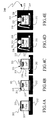
- Figure 1A shows a first implementation step of the method which provides the formation of a photo-resist resin layer above the MEMS device comprised in the electronic device and the successive partial removal of this resin layer prior to the overmoulding of the device in a protective casing.
- a substrate 12 has been shown, for example of the LGA/BGA type comprising an insulating core of a polymeric material (for example triazine and bismaleimide resin (BT)) and coated by metallic layers, for example of copper, wherein, according to conventional techniques, conductive tracks are shaped not shown in the figure.
- a MEMS device 13 is glued serving as sensor, i.e. it is sensitive to chemical and/or physical variations of a fluid present outside the electronic device.
- the MEMS device 13 is integrated in a die, for example of silicon, and has a non active surface 14 and an active surface 15, opposed to the non active surface 14, below which a cavity is present 16. Above the cavity 16 there is a membrane 17 having a top surface that is part of the active surface 15.
- a photo-resist resin layer 21 is deposited, for example of the SU-8 type, through the "spin coating" technique.
- the fundamental characteristic, which makes the SU-8 useful for the ultrathick "photo-resist” applications, is its very low optical absorption in a range of the near-UV radiations, which determines uniform exposure conditions according to the thickness, allows to form perfectly vertical walls and to have a good size control on the height of the whole formed structure.
- Another advantage of the SU-8 is its capacity of self-planarization.
- the resin layer 21 deposited has a relatively high thickness greater than 20 ⁇ m.
- the resin layer 21 deposited has a greater thickness than the maximum height of the metallic wires 18, which is equal to 150 micrometres.
- the resin layer 21 is exposed to a radiation being near in the spectrum to UV radiation and an etching of the chemical type or the "ashing" technique, to remove the excess resin layer from a central region 19, overlaying the surface 15 in correspondence with the membrane 17, and from a peripheral region 20 overlaying a peripheral portion of the surface 15.
- This peripheral region 20, is, in fact, apt to house metallic wires 18 serving as electric connections between the MEMS sensor 13 and the substrate 12, which has suitable pads, not shown in the figure, which are connected to the conductive tracks through these conductive wires 18.
- a first and a second portion of the resin layer 21 are left in correspondence with regions 22 overlaying the active surface 15 and adjacent to the central region 19, so that an opening 23 is formed in correspondence with the central region 19, which allows the interaction of the sensor 13, through the membrane 17, with an external fluid.
- the resin layer is deposited by means of the known technique of the "screen printing".
- the resin layer is deposited by means of the known technique of the "dispensing".
- a moulding step of a protective casing (“moulding") is carried out, through conventional techniques.
- An electronic device 10 is thus formed which, in the end, includes the MEMS device 13 overmoulded inside a protective casing or "package" 24.
- the protective casing 24 comprises the MEMS device 13, overlaid by the two residual portions of the resin layer 21, the electric connections 18 and the substrate 12, leaving the opening 23 exposed in correspondence with the membrane 17 of the MEMS device 13.
- the protective casing 24 is in contact with the resin layer 21.
- Figure 2 shows a TEM image from above of the electronic device 10.
- FIG. 3A-3C the steps are shown of a second implementation example of the manufacturing method leading to a second embodiment of the electronic device of the invention comprising MEMS devices.
- This second implementation example provides the formation of the resin layer on a portion of the MEMS device in correspondence with the active membrane and the successive removal of this resin layer after the overmoulding of the device in a protective casing.
- FIG 3A shows a first step of the second implementation example of the method.
- a MEMS device 113 serving as sensor.
- the MEMS device 113 is integrated in a die, for example of silicon, and has a non active surface 114 and an active surface 115 opposed to the non active surface 114. Below the active surface 115, there is a cavity 116, above which there is a membrane 117.
- the MEMS sensor 113 is connected, through conductive wires 118, to the substrate 112 which has pads, not shown in the figure, connected to the conductive tracks.
- a photo-resist resin layer 121 for example of the SU-8 type, is deposited on a region 119 overlaying the active surface 115 of the MEMS sensor 113 in correspondence with the membrane 117, while regions 122 overlaying the active surface 115 and adjacent to the region 119 are not coated by the photo-resist resin.
- the resin layer 121 deposited has a relatively high thickness greater than 20 ⁇ m.
- the resin layer 121 deposited has a thickness greater than the maximum height of the metallic conductive wires 118, which is equal to 150 micrometres.
- the resin layer 121 is deposited through the "spin coating” technique.
- the resin layer 121 is deposited through conventional photolithography.
- the resin layer 121 is deposited through the "screen printing" technique.
- the resin layer is deposited through the "dispensing" technique.
- the moulding step is carried out, through conventional "moulding" techniques, in which inside a protective casing or "package” 124 the MEMS device 113, the electric connections 118 and the substrate 112, are encompassed leaving the resin layer 121 exposed in correspondence with the membrane 117 of the MEMS device 113.
- a final cleaning step is carried out in which the resin layer 121 is totally removed from the region 119 and, in its place, an opening 123 is formed which allows the interaction of the sensor 113 with an external fluid.
- Figure 3C shows the electronic device 110 thus obtained.
- Figures 4A-4E show, by way of example, the steps relative to an application of the second implementation example of the manufacturing method, in case the "dispensing" technique is used for depositing the resin layer.
- figure 4A shows the gluing step, through the known "flip-chip” technique, between a substrate 212 and a MEMS sensor 213 having an active surface 215, below which there are a cavity 216 and a membrane 217 placed above the cavity 216.
- This gluing step is followed, as shown in figure 4B , by a distribution step of photo-resist resin, such as to form an ovoidal region of resin 221 above a region 219 overlaying the active surface 215 in correspondence with the membrane 217.
- the photo-resist resin used to form the ovoidal region 221 is of the SU-8 type.
- This resin region 221 is subsequently subjected to a "curing" thermal process, followed by a step, shown in figure 4C , of electrochemical cleaning, through “plasma cleaning” and of formation of metallic connections 218 between the MEMS sensor 213 and the substrate 212 through “wire bonding".
- Figure 4D shows the overmoulding step, through conventional "moulding" techniques, inside a protective casing or "package” 224, of the MEMS device 213, of the electric connections 218 and of the substrate 212, leaving the resin ovoidal region 221 exposed.
- a final cleaning step follows, from which the device 210 shown in figure 4E is obtained, wherein the resin region 221 is totally removed, leaving an opening 223 in correspondence with the region 219, which allows the interaction of the sensor 213 with an external fluid.
- Figures 5A, 5B show two TEM images (Transmitted Electronic Microscopy) of two portions of the device 210.
- figure 5A shows the TEM image of the step shown in figure 4C
- figure 5B shows the TEM image from above of a stripe of the device 210.
- the method according to the invention has a further advantage in that it allows to realise a device comprising three-dimensional micro-channels which create a preferred path for the passage of a fluid coming from the outside of the device.
- Figure 6 shows for example a section of an electronic device 310 comprising buried micro-channels, realised with the first implementation example of the method according to the invention.
- the device 310 which can be a pressure or gas sensor device, comprises a monolithic silicon body 311, having a lower surface 312 and an upper surface 313 and comprising a buried cavity 314 which is extended to a certain distance from the upper surface 313 and delimits with the upper surface 313 a flexible membrane 315.
- first photo-resist resin layer 317 On a first lateral region 316 of the upper surface 313 there is a first portion of a first photo-resist resin layer 317 and on a second lateral region 318 of the upper surface 313 there is a second portion of a first photo-resist resin layer 317, formed with the method described in figure 1A and 1B . Between the two portions of the first resin layer 317 a channel region 319 is interposed which communicates through an access opening 320 with the buried cavity 314, forming a micro-channel structure. On the portion of resin layer 317 overlaying the lateral region 316 there is a first portion of a second resin layer 321, which is exactly overlapped onto the first portion of resin layer 317.
- the second portion of the second resin layer 321 On the portion of resin layer 317 overlaying the lateral region 318 there is a second portion of the second resin layer 321, which is overlapped onto the second portion of resin layer 317 and extends beyond the resin layer 317, projecting onto the channel region 319 and is separated from the first portion of the second resin layer 321, through a space 322 communicating with the channel region 319.
- the portions of the second resin layer 321 are formed by reiterating the method of figures 1A and 1B . Subsequently, the "film assisted moulding" is carried out leaving the first resin layer 317 exposed.
- the device 310 is overmoulded, together with the portions of the first and of the second resin layer 317 and 321, in a protective casing or "package” 323 which has an opening 324 in correspondence with the space 322, through which a fluid present outside the package 324 penetrates inside the channel region 319.
- micro-channels are realised by using a standard photo-lithography. With at least two resin layers a complex structure with three-dimensional channels is realised, like the one shown in figure 7 .
- the sizes of the channels and of the surface etched in the silicon are smaller, of at least one order of magnitude, than the structure realised with the device overmoulding technologies, have the photolithographic accuracy and are compatible with the front end processes.
Landscapes
- Engineering & Computer Science (AREA)
- Microelectronics & Electronic Packaging (AREA)
- Manufacturing & Machinery (AREA)
- Micromachines (AREA)
Abstract
- forming a resin layer (21; 121; 221) on the membrane (17; 117; 217);
- removing at least a first portion of the resin layer (21; 121; 221) from the membrane (17; 117; 217), so that an opening (23; 123; 223) is formed over the membrane (17; 117; 217); and
- moulding a protective casing (24; 124; 214) on the MEMS device (13; 113; 213) after forming the resin layer (21; 121; 221),
the opening (23; 123; 223) being apt to allow the MEMS device (13; 113; 213) to be activated from the outside of the protective casing (24; 124; 224).
Description
- The present invention relates to a method for manufacturing an electronic device comprising overmoulded MEMS devices.
- The invention also relates to an electronic device comprising overmoulded MEMS devices.
- The invention particularly, but not exclusively, relates to a method for manufacturing an electronic device comprising MEMS sensors mounted on an LGA substrate, wherein the MEMS sensor needs a physical interface to communicate with the outside of the electronic device and the following description is made with reference to this field of application by way of illustration only.
- As it is well known, a MEMS device (micro-electro-mechanical system) is a miniaturised device or, in any case, a device having micrometric size which integrates mechanical and electrical functions in a chip or die of semiconductor material, for example of silicon, and which is realised by using micro-manufacturing lithographic techniques. The final assembled device is typically made of the silicon die wherein the MEMS device is integrated and, optionally, of integrated circuits for specific applications mounted on a substrate, for example of the LGA or BGA type (Land Grid Array or Ball Grid Array), flanked to or piled onto the MEMS device, by using conventional assembling processes.
- A cover or cap, fixed to the substrate, overmoulds the MEMS device and the other devices mounted on the substrate, forming a casing which protects the MEMS device against external physical stresses.
- If the MEMS device is a pressure, gas, liquid sensor or a microphone, the cover is provided with a window to allow the interaction between the device and the outside of the assembled device.
- It is also known that the substrate of the LGA/BGA type is formed by conductive layers insulated from each other by means of layers of insulating or dielectric material. The conductive layers are shaped in conductive tracks insulated from each other by layers of insulating or dielectric material. Conductive through-holes, called "vias", typically realised through the insulating layers according to an orthogonal orientation with respect to the insulating layers, are provided to form conductive paths between conductive tracks belonging to different conductive layers.
- The MEMS devices are then electrically connected with the outside of the final device through wires connecting contact pads provided on the MEMS devices with conductive tracks present on the substrate inside the cover.
- A solution of this type is described for example in the European patent application, with publication number
EP 1 775 259, filed on October 14, 2005 by the same Applicant. In this patent application a MEMS device, in particular a pressure sensor, is realised on a substrate of the LGA type, to which it is glued, through a layer of epoxy glue. This sensor has a cavity above which there is a membrane and is connected to the substrate through metallic conductive wires. It is then covered by a closing wafer equipped with an opening in correspondence with the membrane of the sensor and through which the sensor is in communication with the outside. All the device is finally overmoulded in a casing. - Although advantageous under several aspects, this solution shows different drawbacks. In fact, the complete device is made by first realising a casing bottom, then the different components are affixed to the casing bottom, and finally the casing is moulded and the element to control the sensor is inserted through the window of the casing. For these devices, moreover, the procedure of alignment and positioning of the window to introduce the element for controlling the sensor is rather complicated, making the realisation of the device difficult to be reproduced. Moreover, the manufacturing process of these devices is complicated by the presence of different assembling steps and relatively expensive.
- A second solution, described in European patent no.
EP 1 211 722, granted on September 8, 2004 to the same Applicant, provides the use of a casing which, by using a conventional technique, is equipped with a window in correspondence with an integrated electronic device, for example a sensor housed inside the casing and which must be put in communication with the outside of the casing. This window is obtained by using the same mould which is used to realise the casing; this mould is equipped with a protrusion projecting internally in correspondence with the sensor. After having fixed the sensor and a relative control circuitry to a semiconductor substrate, which serves as support, a surface of the sensor is covered with a coating layer formed by material of the elastic type. The substrate is inserted in the mould so that the protrusion is in correspondence and in contact with the coating layer. The mould is then filled in by injection with an insulating material to realise, in a single step, the casing with window. - Although meeting the aim, also this solution is not exempt from drawbacks, such as the reproducibility of the process, the stability of the shape of the dispensed elastic material, the reliability and the strength of the device which can, in fact, be subject to delaminations at the interface between the insulating material and the material of the elastic type.
- Another technique for manufacturing a MEMS device overmoulded in a casing uses a moulding machine commercially known as "film assisted mould", which realises the cap of the device thanks to a polymeric film, interposed between the mould and the device itself, which allows to expose the silicon in a remarkably controlled way.
- The disadvantage of this solution consists in that the increase of the size of the holes made on the cap determines a weakening of the silicon slice which serves as cap, and a subsequent breakage of this one during the completion of the device.
- Moreover, to ease the interaction between a MEMS device, for example a pressure sensor, and the fluid outside the casing overmoulding it methods have been implemented for manufacturing micro-channels buried in the MEMS device, below the membrane or active element. A method which realises buried micro-channels of this type is described in the EP patent application, with publication number
EP 1 719 993, filed on May 6, 2005 by the same Applicant. - A second method known for the formation of micro-channels is described in the
US patent application publication No. 2006/0246416 . According to this method, the micro-channels are formed in the substrate of a first "chip", called micro-porous "chip", which is then glued to a second "chip", called micro-fluidic "chip". A third example of formation of micro-channels is described in theUS patent application publication No. 2005/0151244 , wherein micro-channels are formed first in a "cooling plate" using to cool an electronic "chip". - It is known to realize micro-channels in a silicon substrate through the combination of suitably shaped layers.
- Another aspect to be taken into account in the manufacturing of the MEMS devices, in particular in the ultra thin ones, or for "package" applications, is the use of photo-sensitive resins ("photo-resist") being very thick and with high "aspect ratio" (i.e.: with high ratio between width and height of the device, also known as "aspect ratio"), so as to obtain vertical walls in relatively high structures with a good control of the size on the whole height.
- A known technique to obtain structures with high "aspect ratio" with sub-micrometric resolution in very thick "photo-resist" is the X ray lithography, used in the LIGA process ("Lithography, Galvanoforming and Abformung") to form very thick layers of PMMA (polymethylmethacrylate). However, the cost of the manufacturing of a device, made by using the LIGA process with X ray lithography, is strongly influenced by the high cost of the X ray source (synchrotron radiation) and by the complex technology of the masks.
- Recently, instead, a new type of "photo-resist", having characteristics similar to the PMMA and having the possibility of being used in a process of the LIGA type, is used for the applications of ultrathin MEMS with high "aspect ratio".
- The characteristics of this new type of "photo-resist", called SU-8, are described in the publications "A novel fabrication Method of embedded micro channels employing simple UV dosage control and antireflection coating", F.G.Tseng, Y.J.Chuang and W.K.Lin, 2002 IEEE; and "High-Aspect-Ratio, Ultrathick, Negative-tone near-UV photoresist for MEMS applications", M.Despont, H.Lorenz, N.Fahrni, J.Brugger, P.Renaud and P.Vettiger, 1997 IEEE.
- The SU-8 is a "photo-resist" similar to the epoxy resin, sensitive to the radiation near the UV and based onto the resin EPON SU-8 (from "Shell Chemical"). The fundamental characteristic, which makes the SU-8 useful for the ultrathick "photo-resist" applications, is its very low optical absorption in a range of radiations near the UV, which determines uniform exposure conditions according to the thickness, allows to form perfectly vertical walls and to have a good size control on the height of the whole formed structure. Another advantage of the SU-8 is its capacity of self-planarization during the "prebake" and then to eliminate the "edge-bead" effect, determining a good contact between the mask and the "photo-resist" in the contact lithography.
- As reported in the second one of the above publications, it has been proved that, with a coating having single SU-8 layer, thicknesses can be obtained, in a reproducible way, of more than 500 µm and that even thicker "photo-resist" can be obtained through multiple coatings, up to 1200 µm of thickness with a double-layer coating. The "aspect ratio" found for structures exposed to the radiation near the UV (400nm) can be greater than 18 and remains constant for a thickness comprised between 80 and 1200 µm.
- The technical problem underlying the present invention is that of devising a device comprising overmoulded MEMS devices, having such structural and functional characteristics as to allow the realisation of this electronic device with low-cost manufacturing processes overcoming the limits and/or the drawbacks still affecting the electronic devices realised according to the prior art.
- The solution idea underlying the present invention is that of realising a method for manufacturing an electronic device comprising overmoulded MEMS devices, wherein the opening putting the MEMS device in communication with the outside is realised through photolithography with "photo-resist" thick layers, for example of the type known as SU-8.
- On the basis of this solution idea the technical problem is solved by a method for manufacturing an electronic device comprising a MEMS device including the step of
- forming said MEMS device having a membrane sensitive to chemical or physical variations of a fluid, the method being characterised in that it further comprises the steps of:
- forming a resin layer on said membrane;
- removing at least a first portion of said resin layer from said membrane, so that an opening is formed over said membrane; and
- moulding a protective casing on said MEMS device after forming said resin layer,
- Advantageously according to the invention, the opening can be central with respect an active surface of the MEMS device wherein a portion of the MEMS device is integrated.
- Moreover, the step of forming the resin layer can comprise one of the following features:
- depositing the resin layer simultaneously on the membrane, on a peripheral region overlaying an active surface of the MEMS device, and on a first and a second region of the active surface that are adjacent to the membrane;
- depositing the resin layer limitedly on the membrane, without depositing the resin layer on peripheral areas of the active surface of the MEMS device.
- Also, the step of removing at least the first portion of the resin layer can comprise.
- etching simultaneously the resin layer from the membrane and from the peripheral region and leaving the resin layer on the first and second regions;
- forming the opening, which is an opening in the resin layer;
- Furthermore, advantageously according to the invention, the step of removing at least the first portion of the resin layer can be performed prior or after to the moulding step of the protective casing.
- Moreover, the step of forming the resin layer can comprise depositing the resin layer with a spin coating technique, or with a screen printing technique, or with a stencil printing technique, or with a dispensing technique, or through photo-lithography.
- Furthermore, depositing the resin layer with the dispensing technique can comprise forming a resin ovoidal region, which can be subjected to a curing process.
- Also, the resin layer can be photo-sensitive to the near-UV radiation, in particular an SU-8 resin layer with a thickness greater than 20 µm.
- The problem is also solved by an electronic device comprising a MEMS device having a membrane sensitive to chemical or physical variations of a fluid, characterised in that it further comprises first and second portions of a resin layer over said membrane and a protective casing surrounding said MEMS device, which is activated from the outside of said protective casing through an opening placed between said first and second portions of said resin layer, in correspondence with said membrane.
- Finally, the problem is solved by an electronic device, comprising:
- a monolithic body of semiconductor material having a lower surface and an upper surface;
- a buried cavity extending below said upper surface and delimiting, with said upper surface, a flexible membrane;
- an access opening fluidically communicating with said buried cavity;
- a protective casing comprising an opening suitable for putting said electronic device in communication with an external fluid;
- a channel region overlaying said flexible membrane and interposed between a first portion and a second portion of a first resin layer, overlaying said active surface laterally with respect to said flexible membrane, and delimited on top by a second projecting portion of a second resin layer separated from a first portion of a second resin layer through a space communicating below with said channel region and above with said opening;
- The characteristics and the advantages of the method and of the device according to the invention will be apparent from the following description of their respective embodiments given by way of indicative and non limiting example with reference to the annexed drawings.
- In these drawings:
-
figures 1A, 1B show the steps of a first implementation example of the manufacturing method of a first embodiment of the electronic device comprising MEMS devices, according to the invention; -
figure 2 shows a TEM image (Transmitted Electronic Microscopy) from above of the first embodiment of the electronic device offigure 1 comprising MEMS devices, obtained with the method according to the invention; -
figures 3A-3C show the steps of a second implementation example of the manufacturing method of a second embodiment of the electronic device comprising MEMS devices, according to the invention; -
figures 4A-4E show an application of the steps of the second implementation example of the manufacturing method of a second embodiment of the electronic device comprising MEMS devices, according to the invention; -
figures 5A, 5B show the TEM images of two portions of the device obtained with this implementation example of the method, according to the invention; -
figure 6 shows a section of an electronic device realised with the method according to the invention; and -
figure 7 shows a three-dimensional view of the buried micro-channels, realised with the method according to the invention. - With reference to
figures 1A and 1B , the steps are shown of a first implementation example of the manufacturing method of a first embodiment of the electronic device comprising MEMS devices according to the invention. - Hereafter in the description it will be apparent that the method according to the invention can be implemented to obtain indifferently a first or a second embodiment of an electronic device incorporating MEMS devices.
- In the following description it is also taken for granted that the MEMS device has already been realised above a semiconductor substrate of the electronic device housing it.
-
Figure 1A shows a first implementation step of the method which provides the formation of a photo-resist resin layer above the MEMS device comprised in the electronic device and the successive partial removal of this resin layer prior to the overmoulding of the device in a protective casing. - In particular, a
substrate 12 has been shown, for example of the LGA/BGA type comprising an insulating core of a polymeric material (for example triazine and bismaleimide resin (BT)) and coated by metallic layers, for example of copper, wherein, according to conventional techniques, conductive tracks are shaped not shown in the figure. Above the substrate 12 aMEMS device 13 is glued serving as sensor, i.e. it is sensitive to chemical and/or physical variations of a fluid present outside the electronic device. TheMEMS device 13 is integrated in a die, for example of silicon, and has a nonactive surface 14 and anactive surface 15, opposed to the nonactive surface 14, below which a cavity is present 16. Above thecavity 16 there is amembrane 17 having a top surface that is part of theactive surface 15. - Advantageously, on the
whole surface 15 of the MEMS sensor 13 a photo-resistresin layer 21 is deposited, for example of the SU-8 type, through the "spin coating" technique. - The fundamental characteristic, which makes the SU-8 useful for the ultrathick "photo-resist" applications, is its very low optical absorption in a range of the near-UV radiations, which determines uniform exposure conditions according to the thickness, allows to form perfectly vertical walls and to have a good size control on the height of the whole formed structure. Another advantage of the SU-8 is its capacity of self-planarization.
- Advantageously, the
resin layer 21 deposited has a relatively high thickness greater than 20 µm. - Advantageously, the
resin layer 21 deposited has a greater thickness than the maximum height of themetallic wires 18, which is equal to 150 micrometres. - Subsequently, the
resin layer 21 is exposed to a radiation being near in the spectrum to UV radiation and an etching of the chemical type or the "ashing" technique, to remove the excess resin layer from acentral region 19, overlaying thesurface 15 in correspondence with themembrane 17, and from aperipheral region 20 overlaying a peripheral portion of thesurface 15. Thisperipheral region 20, is, in fact, apt to housemetallic wires 18 serving as electric connections between theMEMS sensor 13 and thesubstrate 12, which has suitable pads, not shown in the figure, which are connected to the conductive tracks through theseconductive wires 18. - Finally, a first and a second portion of the
resin layer 21 are left in correspondence withregions 22 overlaying theactive surface 15 and adjacent to thecentral region 19, so that anopening 23 is formed in correspondence with thecentral region 19, which allows the interaction of thesensor 13, through themembrane 17, with an external fluid. - Advantageously, according to another aspect of the invention, the resin layer is deposited by means of the known technique of the "screen printing".
- Advantageously, according to another aspect of the invention, the resin layer is deposited by means of the known technique of the "dispensing".
- Subsequently, as shown in
figure 1B a moulding step of a protective casing ("moulding") is carried out, through conventional techniques. Anelectronic device 10 is thus formed which, in the end, includes theMEMS device 13 overmoulded inside a protective casing or "package" 24. In particular, theprotective casing 24 comprises theMEMS device 13, overlaid by the two residual portions of theresin layer 21, theelectric connections 18 and thesubstrate 12, leaving theopening 23 exposed in correspondence with themembrane 17 of theMEMS device 13. In particular, theprotective casing 24 is in contact with theresin layer 21. -
Figure 2 shows a TEM image from above of theelectronic device 10. - With reference to
figures 3A-3C , the steps are shown of a second implementation example of the manufacturing method leading to a second embodiment of the electronic device of the invention comprising MEMS devices. This second implementation example provides the formation of the resin layer on a portion of the MEMS device in correspondence with the active membrane and the successive removal of this resin layer after the overmoulding of the device in a protective casing. -
Figure 3A shows a first step of the second implementation example of the method. On asubstrate 112 is glued aMEMS device 113 serving as sensor. TheMEMS device 113 is integrated in a die, for example of silicon, and has a nonactive surface 114 and anactive surface 115 opposed to the nonactive surface 114. Below theactive surface 115, there is acavity 116, above which there is amembrane 117. TheMEMS sensor 113 is connected, throughconductive wires 118, to thesubstrate 112 which has pads, not shown in the figure, connected to the conductive tracks. - Advantageously, a photo-resist
resin layer 121, for example of the SU-8 type, is deposited on aregion 119 overlaying theactive surface 115 of theMEMS sensor 113 in correspondence with themembrane 117, whileregions 122 overlaying theactive surface 115 and adjacent to theregion 119 are not coated by the photo-resist resin. - Advantageously, the
resin layer 121 deposited has a relatively high thickness greater than 20 µm. - Advantageously, the
resin layer 121 deposited has a thickness greater than the maximum height of the metallicconductive wires 118, which is equal to 150 micrometres. - Advantageously, according to another aspect of the invention, the
resin layer 121 is deposited through the "spin coating" technique. - Advantageously, according to another aspect of the invention, the
resin layer 121 is deposited through conventional photolithography. - Advantageously, according to another aspect of the invention, the
resin layer 121 is deposited through the "screen printing" technique. - Advantageously, according to another aspect of the invention, the resin layer is deposited through the "dispensing" technique.
- Subsequently, as shown in
figure 3B , the moulding step is carried out, through conventional "moulding" techniques, in which inside a protective casing or "package" 124 theMEMS device 113, theelectric connections 118 and thesubstrate 112, are encompassed leaving theresin layer 121 exposed in correspondence with themembrane 117 of theMEMS device 113. - Subsequently, a final cleaning step is carried out in which the
resin layer 121 is totally removed from theregion 119 and, in its place, anopening 123 is formed which allows the interaction of thesensor 113 with an external fluid.Figure 3C , corresponding to this step, shows theelectronic device 110 thus obtained. -
Figures 4A-4E show, by way of example, the steps relative to an application of the second implementation example of the manufacturing method, in case the "dispensing" technique is used for depositing the resin layer. - In particular,
figure 4A shows the gluing step, through the known "flip-chip" technique, between asubstrate 212 and aMEMS sensor 213 having anactive surface 215, below which there are acavity 216 and amembrane 217 placed above thecavity 216. This gluing step is followed, as shown infigure 4B , by a distribution step of photo-resist resin, such as to form an ovoidal region ofresin 221 above aregion 219 overlaying theactive surface 215 in correspondence with themembrane 217. - Advantageously, the photo-resist resin used to form the
ovoidal region 221 is of the SU-8 type. - This
resin region 221 is subsequently subjected to a "curing" thermal process, followed by a step, shown infigure 4C , of electrochemical cleaning, through "plasma cleaning" and of formation ofmetallic connections 218 between theMEMS sensor 213 and thesubstrate 212 through "wire bonding". -
Figure 4D shows the overmoulding step, through conventional "moulding" techniques, inside a protective casing or "package" 224, of theMEMS device 213, of theelectric connections 218 and of thesubstrate 212, leaving theresin ovoidal region 221 exposed. - A final cleaning step follows, from which the
device 210 shown infigure 4E is obtained, wherein theresin region 221 is totally removed, leaving anopening 223 in correspondence with theregion 219, which allows the interaction of thesensor 213 with an external fluid. -
Figures 5A, 5B show two TEM images (Transmitted Electronic Microscopy) of two portions of thedevice 210. In particular,figure 5A shows the TEM image of the step shown infigure 4C , whilefigure 5B shows the TEM image from above of a stripe of thedevice 210. - The method according to the invention has a further advantage in that it allows to realise a device comprising three-dimensional micro-channels which create a preferred path for the passage of a fluid coming from the outside of the device.
-
Figure 6 shows for example a section of anelectronic device 310 comprising buried micro-channels, realised with the first implementation example of the method according to the invention. - In particular, the
device 310, which can be a pressure or gas sensor device, comprises amonolithic silicon body 311, having alower surface 312 and anupper surface 313 and comprising a buriedcavity 314 which is extended to a certain distance from theupper surface 313 and delimits with the upper surface 313 aflexible membrane 315. - On a first
lateral region 316 of theupper surface 313 there is a first portion of a first photo-resistresin layer 317 and on a secondlateral region 318 of theupper surface 313 there is a second portion of a first photo-resistresin layer 317, formed with the method described infigure 1A and 1B . Between the two portions of the first resin layer 317 achannel region 319 is interposed which communicates through an access opening 320 with the buriedcavity 314, forming a micro-channel structure. On the portion ofresin layer 317 overlaying thelateral region 316 there is a first portion of asecond resin layer 321, which is exactly overlapped onto the first portion ofresin layer 317. On the portion ofresin layer 317 overlaying thelateral region 318 there is a second portion of thesecond resin layer 321, which is overlapped onto the second portion ofresin layer 317 and extends beyond theresin layer 317, projecting onto thechannel region 319 and is separated from the first portion of thesecond resin layer 321, through aspace 322 communicating with thechannel region 319. The portions of thesecond resin layer 321 are formed by reiterating the method offigures 1A and 1B . Subsequently, the "film assisted moulding" is carried out leaving thefirst resin layer 317 exposed. - The
device 310 is overmoulded, together with the portions of the first and of thesecond resin layer opening 324 in correspondence with thespace 322, through which a fluid present outside thepackage 324 penetrates inside thechannel region 319. - The micro-channels are realised by using a standard photo-lithography. With at least two resin layers a complex structure with three-dimensional channels is realised, like the one shown in
figure 7 . - In conclusion, the method according to the invention allows to realise economic pressure sensors with other "aspect ratio".
- With the method according to the invention it is also possible to realise on the chip a preferred path for gases or liquids flowing inside the package up to the sensor. This method, in fact, can be applied to gas, pressure and chip sensors used in micro-fluidic.
- Moreover, the sizes of the channels and of the surface etched in the silicon are smaller, of at least one order of magnitude, than the structure realised with the device overmoulding technologies, have the photolithographic accuracy and are compatible with the front end processes.
- From the foregoing it will be appreciated that, although specific embodiments of the invention have been described herein for purposes of illustration, various modifications may be made without deviating from the spirit and scope of the invention. Accordingly, the invention is not limited except as by the appended claims.
Claims (20)
- A method for manufacturing an electronic device (10; 110; 210) comprising a MEMS device (13; 113; 213) including the step of- forming said MEMS device (13; 113; 213) having a membrane (17; 117; 217) sensitive to chemical or physical variations of a fluid, characterised in that it further comprises the steps of:- forming a resin layer (21; 121; 221) on said membrane (17; 117; 217);- removing at least a first portion of said resin layer (21; 121; 221) from said membrane (17; 117; 217), so that an opening (23; 123; 223) is formed over said membrane (17; 117; 217); and- moulding a protective casing (24; 124; 214) on said MEMS device (13; 113; 213) after forming said resin layer (21; 121; 221),said opening (23; 123; 223) being apt to allow said MEMS device (13; 113; 213) to be activated from the outside of said protective casing (24; 124; 224).
- A method according to claim 1, characterised in that said opening (23; 123; 223) is central with respect an active surface (15; 115; 215) of said MEMS device (13; 113; 213) wherein a portion of said MEMS device is integrated.
- A method according to claim 1, characterised in that said step of forming said resin layer (21; 121; 221) comprises depositing said resin layer (21) simultaneously on said membrane (17; 117; 217), on a peripheral region (20) overlaying an active surface (15) of said MEMS device (13; 113; 213), and on a first and a second region (22) of said active surface (15) that are adjacent to said membrane (17; 117; 217).
- A method according to claim 1, characterised in that said step of forming said resin layer (21; 121; 221) comprises depositing said resin layer (121) limitedly on said membrane (17; 117; 217).
- A method according to claim 3, characterised in that said step of removing at least said first portion of said resin layer (21; 121; 221) comprises etching simultaneously said resin layer (21) from said membrane (17; 117; 217) and from said peripheral region (20) and leaving said resin layer (21) on said first and second regions (22).
- A method according to claim 1, characterised in that said step of removing at least said first portion of said resin layer (21; 121; 221) comprises forming said opening (23), which is an opening in said resin layer (21).
- A method according to claim 1, characterised in that said step of removing at least said first portion of said resin layer (21; 121; 221) is performed prior to the moulding step of said protective casing (24).
- A method according to claim 1, characterised in that said step of removing at least said fist portion of said resin layer (21; 121; 221) is performed after to the moulding step of said protective casing (24).
- A method according to claim 1, characterised in that said step of forming said resin layer (21; 121; 221) comprises depositing said resin layer (21; 121; 221) with a spin coating technique.
- A method according to claim 1, characterised in that said step of forming said resin layer (21; 121; 221) comprises depositing said resin layer (21; 121; 221) with a screen printing technique.
- A method according to claim 1, characterised in that said step of forming said resin layer (21; 121; 221) comprises depositing said resin layer (21; 121; 221) with a stencil printing technique.
- A method according to claim 1, characterised in that said step of forming said resin layer (21; 121; 221) comprises depositing said resin layer (21; 121; 221) with a dispensing technique.
- A method according to claim 12, characterised in that depositing said resin layer (21; 121; 221) with the dispensing technique comprises forming a resin ovoidal region (221).
- A method according to claim 13, characterised in that said resin ovoidal region (221) is subjected to a curing process.
- A method according to claim 1, characterised in that said step of forming said resin layer (121) comprises depositing said resin layer (121) through photo-lithography.
- A method according to claim 1, characterised in that said resin layer (21, 121) is photo-sensitive to the near-UV radiation.
- A method according to claim 1, characterised in that said resin layer (21, 121) is an SU-8 resin layer.
- A method according to claim 1, characterised in that said resin layer (21, 121) has a thickness greater than 20 µm.
- An electronic device (10) comprising a MEMS device (13) having a membrane (17) sensitive to chemical or physical variations of a fluid, characterised in that it further comprises first and second portions of a resin layer (21) over said membrane (17) and a protective casing (24) surrounding said MEMS device (13), which is activated from the outside of said protective casing (24) through an opening (23) placed between said first and second portions of said resin layer (21), in correspondence with said membrane (17).
- An electronic device (310), comprising:- a monolithic body (311) of semiconductor material having a lower surface (312) and an upper surface (313);- a buried cavity (314) extending below said upper surface (313) and delimiting, with said upper surface (313), a flexible membrane (315);- an access opening (320) fluidically communicating with said buried cavity (314);- a protective casing (323) comprising an opening (324) suitable for putting said electronic device (310) in communication with an external fluid;characterised in that it comprises:- a channel region (319) overlaying said flexible membrane (315) and interposed between a first portion and a second portion of a first resin layer (316), overlaying said active surface (312) laterally with respect to said flexible membrane (315), and delimited on top by a second projecting portion of a second resin layer (320) separated from a first portion of a second resin layer (321) through a space (322) communicating below with said channel region (319) and above with said opening (324);and in that said channel region (319) communicates with said cavity (314) through said access opening (320) and with an external fluid through said space (322).
Applications Claiming Priority (1)
| Application Number | Priority Date | Filing Date | Title |
|---|---|---|---|
| IT002099A ITMI20072099A1 (en) | 2007-10-30 | 2007-10-30 | METHOD OF MANUFACTURE OF AN ELECTRONIC DEVICE INCLUDING MEMS ENCAPSED MOLDING DEVICES |
Publications (2)
| Publication Number | Publication Date |
|---|---|
| EP2055668A2 true EP2055668A2 (en) | 2009-05-06 |
| EP2055668A3 EP2055668A3 (en) | 2011-03-09 |
Family
ID=40193511
Family Applications (1)
| Application Number | Title | Priority Date | Filing Date |
|---|---|---|---|
| EP08018860A Withdrawn EP2055668A3 (en) | 2007-10-30 | 2008-10-29 | Manufacturing method of an electronic device including overmoulded MEMS devices |
Country Status (3)
| Country | Link |
|---|---|
| US (2) | US20090115008A1 (en) |
| EP (1) | EP2055668A3 (en) |
| IT (1) | ITMI20072099A1 (en) |
Cited By (2)
| Publication number | Priority date | Publication date | Assignee | Title |
|---|---|---|---|---|
| WO2010093316A1 (en) * | 2009-02-12 | 2010-08-19 | Senseair Ab | A construction unit, comprising a light detector, and a process to assemble such construction unit to a carrier, such as printed circuit card |
| CN106415212A (en) * | 2013-12-12 | 2017-02-15 | Sc2N公司 | measuring sensor |
Families Citing this family (14)
| Publication number | Priority date | Publication date | Assignee | Title |
|---|---|---|---|---|
| US8618620B2 (en) | 2010-07-13 | 2013-12-31 | Infineon Technologies Ag | Pressure sensor package systems and methods |
| US8729697B2 (en) * | 2012-01-09 | 2014-05-20 | Infineon Technologies Ag | Sensor arrangement, a measurement circuit, chip-packages and a method for forming a sensor arrangement |
| US8872288B2 (en) | 2012-08-09 | 2014-10-28 | Infineon Technologies Ag | Apparatus comprising and a method for manufacturing an embedded MEMS device |
| US8809973B2 (en) * | 2013-01-23 | 2014-08-19 | Infineon Technologies Ag | Chip package comprising a microphone structure and a method of manufacturing the same |
| US9677950B2 (en) | 2013-03-14 | 2017-06-13 | Robert Bosch Gmbh | Portable device with temperature sensing |
| ITTO20130651A1 (en) | 2013-07-31 | 2015-02-01 | St Microelectronics Srl | PROCESS OF MANUFACTURING AN ENCAPSULATED DEVICE, IN PARTICULAR AN ENCAPSULATED MICRO-ELECTRO-MECHANICAL SENSOR, EQUIPPED WITH AN ACCESSIBLE STRUCTURE, AS A MEMS MICROPHONE AND ENCAPSULATED DEVICE SO OBTAINED |
| CN106461439B (en) * | 2014-07-30 | 2019-08-16 | 日立汽车系统株式会社 | Sensor and method of making the same |
| US9461192B2 (en) | 2014-12-16 | 2016-10-04 | Sunpower Corporation | Thick damage buffer for foil-based metallization of solar cells |
| ITUB20155716A1 (en) * | 2015-11-19 | 2017-05-19 | St Microelectronics Srl | MICRO-ELECTRO-MECHANICAL DEVICE EQUIPPED WITH TWO CAVITIES AND RELATIVE PROCESS OF MANUFACTURE |
| US20170240418A1 (en) * | 2016-02-18 | 2017-08-24 | Knowles Electronics, Llc | Low-cost miniature mems vibration sensor |
| US10676347B2 (en) | 2018-01-09 | 2020-06-09 | Stmicroelectronics S.R.L. | Micro-electro-mechanical device having two buried cavities and manufacturing process thereof |
| KR102509330B1 (en) | 2018-04-16 | 2023-03-14 | 에스케이하이닉스 주식회사 | Sampling Circuit and Semiconductor Memory Apparatus Using the Same |
| US11865581B2 (en) | 2018-11-21 | 2024-01-09 | Stmicroelectronics S.R.L. | Ultrasonic MEMS acoustic transducer with reduced stress sensitivity and manufacturing process thereof |
| IT201900005808A1 (en) | 2019-04-15 | 2020-10-15 | St Microelectronics Srl | MICROPUMP MEMS DEVICE FOR HANDLING OR EJECTION OF A FLUID, IN PARTICULAR MICROSOFT OR FLOWMETER |
Citations (5)
| Publication number | Priority date | Publication date | Assignee | Title |
|---|---|---|---|---|
| EP1211722A1 (en) | 2000-11-30 | 2002-06-05 | STMicroelectronics S.r.l. | Manufacturing method of electronic device package |
| US20050151244A1 (en) | 2003-12-29 | 2005-07-14 | Intel Corporation | Integrated micro channels and manifold/plenum using separate silicon or low-cost polycrystalline silicon |
| US20060246416A1 (en) | 2003-07-31 | 2006-11-02 | Hirofumi Tani | On-chip bioassay method and kit |
| EP1719993A1 (en) | 2005-05-06 | 2006-11-08 | STMicroelectronics S.r.l. | Integrated differential pressure sensor and manufacturing process thereof |
| EP1775259A1 (en) | 2005-10-14 | 2007-04-18 | STMicroelectronics S.r.l. | Wafer level package for sensor devices |
Family Cites Families (29)
| Publication number | Priority date | Publication date | Assignee | Title |
|---|---|---|---|---|
| US498707A (en) * | 1893-05-30 | Copper-coating the hulls of vessels | ||
| JPH0724287B2 (en) * | 1987-02-12 | 1995-03-15 | 三菱電機株式会社 | Semiconductor device having light transmitting window and method of manufacturing the same |
| US4823605A (en) * | 1987-03-18 | 1989-04-25 | Siemens Aktiengesellschaft | Semiconductor pressure sensor with casing and method for its manufacture |
| US5105262A (en) * | 1988-09-19 | 1992-04-14 | Ford Motor Company | Thick film circuit housing assembly design |
| JPH042152A (en) | 1990-04-19 | 1992-01-07 | Mitsubishi Electric Corp | Resin-sealed semiconductor device, and manufacture thereof |
| IT1252197B (en) | 1991-12-12 | 1995-06-05 | Sgs Thomson Microelectronics | INTEGRATED CIRCUIT PROTECTION DEVICE ASSOCIATED WITH RELATED SUPPORTS. |
| JPH05203522A (en) * | 1992-01-23 | 1993-08-10 | Mitsubishi Electric Corp | Mold package semiconductor pressure sensor and manufacturing method thereof |
| KR960009089B1 (en) * | 1993-03-04 | 1996-07-10 | 문정환 | Mold for package molding and plastic charge-coupled device and the manufacturing method using the mold |
| KR970005706B1 (en) * | 1994-01-24 | 1997-04-19 | 금성일렉트론 주식회사 | Ccd and the manufacturing method |
| JPH09222372A (en) * | 1996-02-19 | 1997-08-26 | Mitsubishi Electric Corp | Semiconductor type sensor |
| JPH09304211A (en) | 1996-05-15 | 1997-11-28 | Omron Corp | Capacitive pressure sensor packaging structure and packaging method |
| NL1003315C2 (en) * | 1996-06-11 | 1997-12-17 | Europ Semiconductor Assembly E | Method for encapsulating an integrated semiconductor circuit. |
| US5948991A (en) * | 1996-12-09 | 1999-09-07 | Denso Corporation | Semiconductor physical quantity sensor device having semiconductor sensor chip integrated with semiconductor circuit chip |
| FR2782388B1 (en) * | 1998-08-11 | 2000-11-03 | Trixell Sas | SOLID STATE RADIATION DETECTOR WITH INCREASED LIFE |
| US5978991A (en) * | 1998-11-16 | 1999-11-09 | Miles; William J. | Device for relieving weight of a blanket on feet and supporting feet of paralyzed persons |
| JP3367458B2 (en) * | 1999-03-30 | 2003-01-14 | 株式会社デンソー | Method for manufacturing semiconductor device |
| IL133453A0 (en) * | 1999-12-10 | 2001-04-30 | Shellcase Ltd | Methods for producing packaged integrated circuit devices and packaged integrated circuit devices produced thereby |
| AT410727B (en) * | 2000-03-14 | 2003-07-25 | Austria Mikrosysteme Int | METHOD FOR PLACING SENSORS IN A HOUSING |
| US6379988B1 (en) * | 2000-05-16 | 2002-04-30 | Sandia Corporation | Pre-release plastic packaging of MEMS and IMEMS devices |
| EP1211721A1 (en) * | 2000-11-30 | 2002-06-05 | STMicroelectronics S.r.l. | Improved electronic device package and corresponding manufacturing method |
| DE10246283B3 (en) * | 2002-10-02 | 2004-03-25 | Infineon Technologies Ag | Production of an electronic component used in semiconductor sensors comprises preparing a semiconductor chip on a switching substrate, applying a sacrificial part on the sensor region of the chip and further processing |
| DE10324139B4 (en) * | 2003-05-26 | 2005-07-21 | Infineon Technologies Ag | Microelectromechanical component and method for its production |
| JP5174673B2 (en) | 2005-10-14 | 2013-04-03 | エスティーマイクロエレクトロニクス エス.アール.エル. | Electronic device with substrate level assembly and method of manufacturing the same |
| TWI395258B (en) * | 2005-11-11 | 2013-05-01 | Semiconductor Energy Lab | Manufacturing method of microstructure and microelectromechanical system |
| DE102005054177B4 (en) * | 2005-11-14 | 2011-12-22 | Infineon Technologies Ag | A method of manufacturing a plurality of packaged sensor modules |
| EP1795496A2 (en) * | 2005-12-08 | 2007-06-13 | Yamaha Corporation | Semiconductor device for detecting pressure variations |
| JP4466589B2 (en) | 2006-03-06 | 2010-05-26 | 住友電気工業株式会社 | PON system and terminal device registration method |
| TWI313501B (en) * | 2006-03-22 | 2009-08-11 | Ind Tech Res Inst | A process for manufacture plastic package of mems devices and the structure for the same |
| TWI327769B (en) * | 2006-12-29 | 2010-07-21 | Ind Tech Res Inst | A packaging structure of pressure sensor and a method therefor |
-
2007
- 2007-10-30 IT IT002099A patent/ITMI20072099A1/en unknown
-
2008
- 2008-10-29 EP EP08018860A patent/EP2055668A3/en not_active Withdrawn
- 2008-10-29 US US12/260,910 patent/US20090115008A1/en not_active Abandoned
-
2010
- 2010-08-02 US US12/848,730 patent/US8324007B2/en not_active Expired - Fee Related
Patent Citations (5)
| Publication number | Priority date | Publication date | Assignee | Title |
|---|---|---|---|---|
| EP1211722A1 (en) | 2000-11-30 | 2002-06-05 | STMicroelectronics S.r.l. | Manufacturing method of electronic device package |
| US20060246416A1 (en) | 2003-07-31 | 2006-11-02 | Hirofumi Tani | On-chip bioassay method and kit |
| US20050151244A1 (en) | 2003-12-29 | 2005-07-14 | Intel Corporation | Integrated micro channels and manifold/plenum using separate silicon or low-cost polycrystalline silicon |
| EP1719993A1 (en) | 2005-05-06 | 2006-11-08 | STMicroelectronics S.r.l. | Integrated differential pressure sensor and manufacturing process thereof |
| EP1775259A1 (en) | 2005-10-14 | 2007-04-18 | STMicroelectronics S.r.l. | Wafer level package for sensor devices |
Non-Patent Citations (2)
| Title |
|---|
| F.G.TSENG; Y.J.CHUANG; W.K.LIN: "IEEE", 2002, article "A novel fabrication Method of embedded micro channels employing simple UV dosage control and antireflection coating" |
| M. DESPONT ET AL.: "High-Aspect-Ratio, U trathick, Negative-tone near-UV photoresist for MEMS applications", IEEE, 1997 |
Cited By (3)
| Publication number | Priority date | Publication date | Assignee | Title |
|---|---|---|---|---|
| WO2010093316A1 (en) * | 2009-02-12 | 2010-08-19 | Senseair Ab | A construction unit, comprising a light detector, and a process to assemble such construction unit to a carrier, such as printed circuit card |
| CN106415212A (en) * | 2013-12-12 | 2017-02-15 | Sc2N公司 | measuring sensor |
| CN106415212B (en) * | 2013-12-12 | 2019-05-31 | Sc2N公司 | Measurement sensor |
Also Published As
| Publication number | Publication date |
|---|---|
| ITMI20072099A1 (en) | 2009-04-30 |
| US20090115008A1 (en) | 2009-05-07 |
| US8324007B2 (en) | 2012-12-04 |
| US20100297797A1 (en) | 2010-11-25 |
| EP2055668A3 (en) | 2011-03-09 |
Similar Documents
| Publication | Publication Date | Title |
|---|---|---|
| US8324007B2 (en) | Manufacturing method of an electronic device including overmolded MEMS devices | |
| US8847340B2 (en) | Packaged sensor structure having sensor opening and package opening aligned with sensor element | |
| CN101417783B (en) | Micromechanical device and method of manufacturing micromechanical device | |
| KR101944128B1 (en) | Method for manufacturing a sensor chip comprising a device for testing it | |
| CN101123231B (en) | Micro-electromechanical system wafer-level chip-scale packaging structure and manufacturing method thereof | |
| JP5551934B2 (en) | MEMS device and manufacturing method thereof | |
| US9771259B2 (en) | Method for fabricating electronic device package | |
| US7807506B2 (en) | Microelectromechanical semiconductor component with cavity structure and method for producing the same | |
| KR20140033211A (en) | Process for a sealed mems device with a portion exposed to the environment | |
| US10858245B2 (en) | Deposition of protective material at wafer level in front end for early stage particle and moisture protection | |
| US12188839B2 (en) | Sensor device including sensor unit for a gaseous medium | |
| US20110012214A1 (en) | Microelectromechanical semiconductor component with cavity structure and method for producing the same | |
| JP4675945B2 (en) | Semiconductor device | |
| US7598118B2 (en) | Method of manufacturing semiconductor sensor | |
| CN112110409B (en) | Semiconductor device and method for manufacturing semiconductor device | |
| EP1211722A1 (en) | Manufacturing method of electronic device package | |
| US20250233037A1 (en) | Cavity integrated circuit |
Legal Events
| Date | Code | Title | Description |
|---|---|---|---|
| PUAI | Public reference made under article 153(3) epc to a published international application that has entered the european phase |
Free format text: ORIGINAL CODE: 0009012 |
|
| AK | Designated contracting states |
Kind code of ref document: A2 Designated state(s): AT BE BG CH CY CZ DE DK EE ES FI FR GB GR HR HU IE IS IT LI LT LU LV MC MT NL NO PL PT RO SE SI SK TR |
|
| AX | Request for extension of the european patent |
Extension state: AL BA MK RS |
|
| RIN1 | Information on inventor provided before grant (corrected) |
Inventor name: SHAW, MARK, ANDREW Inventor name: ZIGLIOLI, FREDERICO, GIOVANNI |
|
| RAP1 | Party data changed (applicant data changed or rights of an application transferred) |
Owner name: STMICROELECTRONICS SRL |
|
| 17P | Request for examination filed |
Effective date: 20100922 |
|
| PUAL | Search report despatched |
Free format text: ORIGINAL CODE: 0009013 |
|
| AK | Designated contracting states |
Kind code of ref document: A3 Designated state(s): AT BE BG CH CY CZ DE DK EE ES FI FR GB GR HR HU IE IS IT LI LT LU LV MC MT NL NO PL PT RO SE SI SK TR |
|
| AX | Request for extension of the european patent |
Extension state: AL BA MK RS |
|
| AKX | Designation fees paid |
Designated state(s): DE FR GB IT |
|
| RAP1 | Party data changed (applicant data changed or rights of an application transferred) |
Owner name: STMICROELECTRONICS SRL |
|
| 17Q | First examination report despatched |
Effective date: 20130930 |
|
| STAA | Information on the status of an ep patent application or granted ep patent |
Free format text: STATUS: THE APPLICATION IS DEEMED TO BE WITHDRAWN |
|
| 18D | Application deemed to be withdrawn |
Effective date: 20150501 |