EP2052855A2 - Barrier film and device - Google Patents
Barrier film and device Download PDFInfo
- Publication number
- EP2052855A2 EP2052855A2 EP20080008940 EP08008940A EP2052855A2 EP 2052855 A2 EP2052855 A2 EP 2052855A2 EP 20080008940 EP20080008940 EP 20080008940 EP 08008940 A EP08008940 A EP 08008940A EP 2052855 A2 EP2052855 A2 EP 2052855A2
- Authority
- EP
- European Patent Office
- Prior art keywords
- layer
- barrier film
- organic
- film according
- easy adhesive
- Prior art date
- Legal status (The legal status is an assumption and is not a legal conclusion. Google has not performed a legal analysis and makes no representation as to the accuracy of the status listed.)
- Granted
Links
- AUBOCPGIGWSTNB-UHFFFAOYSA-N CC1CC(C)(C)CC(C)(C)C1 Chemical compound CC1CC(C)(C)CC(C)(C)C1 AUBOCPGIGWSTNB-UHFFFAOYSA-N 0.000 description 1
- IVIIZHWQTKWCEO-UHFFFAOYSA-N CCC1C=C(CC)C=CC1 Chemical compound CCC1C=C(CC)C=CC1 IVIIZHWQTKWCEO-UHFFFAOYSA-N 0.000 description 1
Images
Classifications
-
- B—PERFORMING OPERATIONS; TRANSPORTING
- B32—LAYERED PRODUCTS
- B32B—LAYERED PRODUCTS, i.e. PRODUCTS BUILT-UP OF STRATA OF FLAT OR NON-FLAT, e.g. CELLULAR OR HONEYCOMB, FORM
- B32B27/00—Layered products comprising a layer of synthetic resin
- B32B27/36—Layered products comprising a layer of synthetic resin comprising polyesters
-
- C—CHEMISTRY; METALLURGY
- C08—ORGANIC MACROMOLECULAR COMPOUNDS; THEIR PREPARATION OR CHEMICAL WORKING-UP; COMPOSITIONS BASED THEREON
- C08G—MACROMOLECULAR COMPOUNDS OBTAINED OTHERWISE THAN BY REACTIONS ONLY INVOLVING UNSATURATED CARBON-TO-CARBON BONDS
- C08G18/00—Polymeric products of isocyanates or isothiocyanates
- C08G18/06—Polymeric products of isocyanates or isothiocyanates with compounds having active hydrogen
- C08G18/28—Polymeric products of isocyanates or isothiocyanates with compounds having active hydrogen characterised by the compounds used containing active hydrogen
- C08G18/40—High-molecular-weight compounds
- C08G18/62—Polymers of compounds having carbon-to-carbon double bonds
- C08G18/6216—Polymers of alpha-beta ethylenically unsaturated carboxylic acids or of derivatives thereof
- C08G18/625—Polymers of alpha-beta ethylenically unsaturated carboxylic acids; hydrolyzed polymers of esters of these acids
- C08G18/6254—Polymers of alpha-beta ethylenically unsaturated carboxylic acids and of esters of these acids containing hydroxy groups
-
- C—CHEMISTRY; METALLURGY
- C08—ORGANIC MACROMOLECULAR COMPOUNDS; THEIR PREPARATION OR CHEMICAL WORKING-UP; COMPOSITIONS BASED THEREON
- C08G—MACROMOLECULAR COMPOUNDS OBTAINED OTHERWISE THAN BY REACTIONS ONLY INVOLVING UNSATURATED CARBON-TO-CARBON BONDS
- C08G18/00—Polymeric products of isocyanates or isothiocyanates
- C08G18/06—Polymeric products of isocyanates or isothiocyanates with compounds having active hydrogen
- C08G18/70—Polymeric products of isocyanates or isothiocyanates with compounds having active hydrogen characterised by the isocyanates or isothiocyanates used
- C08G18/72—Polyisocyanates or polyisothiocyanates
- C08G18/77—Polyisocyanates or polyisothiocyanates having heteroatoms in addition to the isocyanate or isothiocyanate nitrogen and oxygen or sulfur
- C08G18/78—Nitrogen
- C08G18/79—Nitrogen characterised by the polyisocyanates used, these having groups formed by oligomerisation of isocyanates or isothiocyanates
- C08G18/797—Nitrogen characterised by the polyisocyanates used, these having groups formed by oligomerisation of isocyanates or isothiocyanates containing carbodiimide and/or uretone-imine groups
-
- C—CHEMISTRY; METALLURGY
- C09—DYES; PAINTS; POLISHES; NATURAL RESINS; ADHESIVES; COMPOSITIONS NOT OTHERWISE PROVIDED FOR; APPLICATIONS OF MATERIALS NOT OTHERWISE PROVIDED FOR
- C09D—COATING COMPOSITIONS, e.g. PAINTS, VARNISHES OR LACQUERS; FILLING PASTES; CHEMICAL PAINT OR INK REMOVERS; INKS; CORRECTING FLUIDS; WOODSTAINS; PASTES OR SOLIDS FOR COLOURING OR PRINTING; USE OF MATERIALS THEREFOR
- C09D175/00—Coating compositions based on polyureas or polyurethanes; Coating compositions based on derivatives of such polymers
- C09D175/04—Polyurethanes
- C09D175/14—Polyurethanes having carbon-to-carbon unsaturated bonds
- C09D175/16—Polyurethanes having carbon-to-carbon unsaturated bonds having terminal carbon-to-carbon unsaturated bonds
-
- H—ELECTRICITY
- H10—SEMICONDUCTOR DEVICES; ELECTRIC SOLID-STATE DEVICES NOT OTHERWISE PROVIDED FOR
- H10K—ORGANIC ELECTRIC SOLID-STATE DEVICES
- H10K50/00—Organic light-emitting devices
- H10K50/80—Constructional details
- H10K50/84—Passivation; Containers; Encapsulations
- H10K50/844—Encapsulations
-
- H—ELECTRICITY
- H10—SEMICONDUCTOR DEVICES; ELECTRIC SOLID-STATE DEVICES NOT OTHERWISE PROVIDED FOR
- H10K—ORGANIC ELECTRIC SOLID-STATE DEVICES
- H10K2102/00—Constructional details relating to the organic devices covered by this subclass
- H10K2102/301—Details of OLEDs
- H10K2102/311—Flexible OLED
-
- H—ELECTRICITY
- H10—SEMICONDUCTOR DEVICES; ELECTRIC SOLID-STATE DEVICES NOT OTHERWISE PROVIDED FOR
- H10K—ORGANIC ELECTRIC SOLID-STATE DEVICES
- H10K50/00—Organic light-emitting devices
- H10K50/80—Constructional details
- H10K50/84—Passivation; Containers; Encapsulations
-
- Y—GENERAL TAGGING OF NEW TECHNOLOGICAL DEVELOPMENTS; GENERAL TAGGING OF CROSS-SECTIONAL TECHNOLOGIES SPANNING OVER SEVERAL SECTIONS OF THE IPC; TECHNICAL SUBJECTS COVERED BY FORMER USPC CROSS-REFERENCE ART COLLECTIONS [XRACs] AND DIGESTS
- Y10—TECHNICAL SUBJECTS COVERED BY FORMER USPC
- Y10T—TECHNICAL SUBJECTS COVERED BY FORMER US CLASSIFICATION
- Y10T428/00—Stock material or miscellaneous articles
- Y10T428/26—Web or sheet containing structurally defined element or component, the element or component having a specified physical dimension
- Y10T428/263—Coating layer not in excess of 5 mils thick or equivalent
- Y10T428/264—Up to 3 mils
- Y10T428/265—1 mil or less
-
- Y—GENERAL TAGGING OF NEW TECHNOLOGICAL DEVELOPMENTS; GENERAL TAGGING OF CROSS-SECTIONAL TECHNOLOGIES SPANNING OVER SEVERAL SECTIONS OF THE IPC; TECHNICAL SUBJECTS COVERED BY FORMER USPC CROSS-REFERENCE ART COLLECTIONS [XRACs] AND DIGESTS
- Y10—TECHNICAL SUBJECTS COVERED BY FORMER USPC
- Y10T—TECHNICAL SUBJECTS COVERED BY FORMER US CLASSIFICATION
- Y10T428/00—Stock material or miscellaneous articles
- Y10T428/31504—Composite [nonstructural laminate]
- Y10T428/31551—Of polyamidoester [polyurethane, polyisocyanate, polycarbamate, etc.]
-
- Y—GENERAL TAGGING OF NEW TECHNOLOGICAL DEVELOPMENTS; GENERAL TAGGING OF CROSS-SECTIONAL TECHNOLOGIES SPANNING OVER SEVERAL SECTIONS OF THE IPC; TECHNICAL SUBJECTS COVERED BY FORMER USPC CROSS-REFERENCE ART COLLECTIONS [XRACs] AND DIGESTS
- Y10—TECHNICAL SUBJECTS COVERED BY FORMER USPC
- Y10T—TECHNICAL SUBJECTS COVERED BY FORMER US CLASSIFICATION
- Y10T428/00—Stock material or miscellaneous articles
- Y10T428/31504—Composite [nonstructural laminate]
- Y10T428/31551—Of polyamidoester [polyurethane, polyisocyanate, polycarbamate, etc.]
- Y10T428/31565—Next to polyester [polyethylene terephthalate, etc.]
Definitions
- the present invention relates a gas-barrier laminate film (referred to as "barrier film” in the specification) usable in an electronic device material and an optical material and having a good gas-barrier property and to a method thereof.
- barrier film a gas-barrier laminate film
- a barrier film fabricated by forming a thin metal oxide film of aluminium oxide, magnesium oxide or silicon oxide on the surface of a plastic film is widely used for wrapping or packaging articles that require shielding from various gases such as water vapor or oxygen and for wrapping or packaging edibles, industrial articles and medicines for preventing them from being deteriorated.
- plastic films are being used in place of glass substrates that are heavy and readily cracked or broken. As applicable to a roll-to-roll system, plastic films are advantageous in point of cost. However, plastic films are problematic in that their gas-barrier property is not good as compared with that of glass substrates. Therefore, when a plastic film is used in a liquid-crystal display device, then water vapor may penetrate into the liquid-crystal cell, thereby causing display failures.
- JP-A-2003-53881 discloses a barrier film comprising an organic layer having a thickness of 0.01 to 1 ⁇ m and an inorganic layer on a plastic film.
- a polymer of acrylate is quoted as a material of the organic layer and the organic layer is formed in vacuum.
- JP-A-2003-53881 also discloses that the barrier property thereof does not deteriorate when folded.
- JP-A-2005-313560 discloses a barrier film comprising an organic layer having a thickness of 0.1 to 10 ⁇ m and an inorganic layer having a thickness of 20 to 100 nm on a plastic substrate.
- a polymer of acrylate is quoted as a material of the organic layer; and the inorganic layer is composed of SiO, SiN or SiON.
- JP-A-2005-279974 discloses a barrier film in which an organic layer and an inorganic layer are laminated on a plastic film.
- JP-A-2005-279974 discloses the barrier film of which surface roughness Ra of the inorganic layer or the organic layer is 0.7 nm or less and in which a polymer of acrylate is used as the organic layer.
- JP-A-2005-279974 also discloses that the barrier film has folding resistance.
- the organic layer of the barrier film in JP-A-2003-53881 is formed in vacuum, a high barrier property of 0.1 g/m 2 ⁇ day or less cannot be achieved and, furthermore, when the barrier film is folded in curvature radius of 15 mm or less, the barrier property thereof cannot be maintained.
- the barrier film in JP-A-2005-313560 has a water vapor permeability of 0.09 g/m 2 ⁇ day or more, being unsatisfactory for the barrier property. Furthermore, for the barrier film in JP-A-2005-279974 , a high barrier property of 0.01 g/m 2 ⁇ day or less and a satisfying folding resistance have not been achieved.
- the present inventers have an object to provide a barrier film which maintains a high water vapor barrier property when folded.
- the present inventors have assiduously studied and, as a result, have found that the problems of the related arts can be solved by providing an easy adhesive layer between an organic layer containing a resin which is obtained by polymerizing a urethane acrylate and a plastic film, and holding a center liner average roughness low. That is, the following invention is provided as means to solve the problems.
- the barrier film of the invention makes it possible to maintain a high water vapor barrier property even if the barrier film is folded.
- the device of the invention has a high permanence.
- the barrier film and the device of the invention are described in detail hereinunder.
- the description made hereinunder is for some typical embodiments of the invention, to which, however, the invention should not be limited.
- the numerical range expressed by the wording "a number to another number" means the range that falls between the former number indicating the lowermost limit of the range and the latter number indicating the uppermost limit thereof.
- the barrier film of the invention is characterized in that it has a structure in which an easy adhesive layer, an organic layer and an inorganic layer are laminated in that order on one surface or both surfaces of a plastic film, and a center liner average roughness of the surface of the organic layer on the inorganic layer side is 0.5nm or less, and the organic layer contains a resin which is obtained by curing an acrylic monomer having at least two acryloyl groups and at least two urethane groups in one molecule as a polymerizable component.
- the substrate film is generally a plastic film.
- the plastic film usable herein may be any one capable of supporting a laminate of an easy adhesive layer, an organic layer and an inorganic layer; and it may be suitably selected depending on the use and the object thereof.
- the plastic film includes metal supports (e.g., aluminium, copper, stainless), and thermoplastic resins such as polyester resin, methacryl resin, methacrylic acid-maleic anhydride copolymer, polystyrene resin, transparent fluororesin, polyimide, fluoropolyimide resin, polyamide resin, polyamidimide resin, polyetherimide resin, cellulose acylate resin, polyurethane resin, polyether ether ketone resin, polycarbonate resin, alicyclic polyolefin resin, polyarylate resin, polyether sulfone resin, polysulfone resin, cycloolefin copolymer, fluorene ring-modified polycarbonate resin, alicyclic-modified polycarbonate resin, fluorene ring-modified polyester resin, acryloyl compound.
- thermoplastic resins such as polyester resin, methacryl resin, methacrylic acid-maleic anhydride copolymer, polystyrene resin, transparent fluorores
- the plastic film of the invention is used as a substrate of a device such as an organic EL device to be mentioned hereinunder, it is desirable that the plastic film is formed of a heat-resistant material.
- the plastic film is preferably formed of a heat-resistant transparent material having a glass transition temperature (Tg) of not lower than 100°C and/or a linear thermal expansion coefficient of at least 40 ppm/°C. Tg and the linear expansion coefficient may be controlled by the additives to the material.
- the thermoplastic resin of the type includes, for example, polyethylene naphthalate (PEN: 120°C), polycarbonate (PC: 140°C), alicyclic polyolefin (e.g., Nippon Zeon's Zeonoa 1600: 160°C), polyarylate (PAr: 210°C), polyether sulfone (PES: 220°C), polysulfone (PSF: 190°C), cycloolefin copolymer (COC, compound described in JP-A 2001-150584 : 162°C), fluorene ring-modified polycarbonate (BCF-PC, compound described in JP-A 2000-227603 : 225°C), alicyclic-modified polycarbonate (IP-PC, compound described in JP-A 2000-227603 : 205°C), acryloyl compound (compound described in JP-A 2002-80616 : 300°C or more) (the parenthesized data are Tg).
- PEN
- a barrier layer side of the barrier film in which the barrier layer side is a side of which a laminate comprising at least one inorganic layer and at least one organic layer is formed, is directed at the inside of the cell; and the barrier film is preferably provided on the innermost side of the cell, that is, the barrier film is preferably adjacent to the device.
- a retardation value is important, because the barrier film is provided in the inside of the cell inner than the polarizing plate.
- a barrier film comprising a substrate having a retardation value of 10 nm or less is laminated on a circular polarizing plate (1/4 wavelength plate + (1/2 wavelength plate) + liner polarizing plate) or that a barrier film comprising a substrate applicable as a 1/4 wavelength plate and having a retardation value of 100 nm to 180 nm is combined with a linear polarizing plate.
- the substrate having a retardation value of 10 nm or less include a cellulose triacetate (Fuji Film, Fuji TAC), polycarbonate (Teijin Chemicals Ltd., Pureace; Kaneka, ELMECH), cycloolefin polymer (JSR Corp., ARTON; ZEON Corp., ZEONOR), cycloolefin copolymer (Mitsui Chem. Inc., APEL (pellet); Polyplastic Com.,TOPAS), polyallylate (Unitika, U100 (pellet)), transparent polyimide (Mitsubishi Gas Chem. Inc., Neoprium).
- a 1/4 wavelength plate usable is a film which was adjusted to a desired retardation by stretching the above film.
- the plastic film of the invention is usable in devices such as organic EL devices
- the plastic film is transparent, or that is, its light transmittance is generally at least 80%, preferably at least 85%, more preferably at least 90%.
- the light transmittance may be measured according to the method described in JIS-K7105.
- a nontransparent material may be used for the plastic film.
- the nontransparent material includes, for example, polyimide, polyacrylonitrile, known liquid-crystal polymer.
- the thickness of the plastic film for use in the barrier film of the invention may be suitably selected depending on its use. Typically, the thickness may be from 1 to 800 ⁇ m, preferably from 10 to 200 ⁇ m.
- the plastic film may have a functional layer such as a transparent conductive layer, a primer layer, etc. The functional layer is described in detail in JP-A 2006-289627 , paragraphs 0036 to 0038.
- Examples of other functional layers than those are a matting agent layer, a protective layer, an antistatic layer, a planarizing layer, an adhesiveness improving layer, a light shielding layer, an antireflection layer, a hard coat layer, a stress relaxing layer, an antifogging layer, an anti-soiling layer, a printable layer, etc.
- an easy adhesive layer may have a single layer constitution or a two layers constitution.
- the single layer constitution achieves satisfying adhesiveness, and however, the two layers constitution achieves stronger adhesiveness to improve the folding resistance.
- an easy adhesive layer of the invention is a single layer constitution, then the layer is directly laminated on a plastic film.
- the layer is necessary to contain a binder and preferably contains a carbodiimide crosslinking agent, which is described in the easy adhesive structure having a two layers constitution.
- the layer further may include matting agent, surfactant, antistatic addictive and particles for controlling flexibility, if necessary.
- the binder of the easy adhesive layer having a single layer constitution of the invention is not defined, and however, usable are an acrylic resin, a polyurethane resin, a polyester resin and a rubber resin.
- the acrylic resin is a polymer composed of an acrylic acid, a methacrylic acid or a derivatives thereof.
- examples of the acrylic resin include a polymer which is obtained by copolymerizing acrylic acid, methacrylic acid, methylmethacrylate, ethylacrylate, butylacrylate, 2-ethylhexylacrylate, acrylamide, acrylonitrile, hydroxylacrylate and the like, as a main component, with a monomer copolymerizable therewith, for example, styrene and divinylbenzene.
- the polyurethane resin is a generic term of a polymer having a urethane bonding in the main chain, generally obtained by reacting polyisocyanate with polyol.
- polyisocyanate examples include TDI, MDI, NDI TODI, HDI and IPDI and examples of the polyol include ethylene glycol, propylene glycol, glycerin and hexane triol.
- polymer which is obtained by subjecting a urethane polymer obtained by reacting polyisocyanate with polyol to chain elongation treatment, thereby increasing the molecular weight thereof.
- the polyisocyanate, polyol and chain elongation treatment, as described above, for example, are described in "Polyurethane Resin Hand Book" which was edited by IWATA Keizi and issued by Nikkan Kogyo Shimbun on 1987.
- the polyester resin is a generic term of a polymer having an ester bonding in the main chain, generally obtained by reacting polycarboxylic acid and polyol.
- the polycarboxylic acid include fumaric acid, itaconic acid, adipic acid, sebacic acid, terephthalic acid and isophthalic acid and examples of the polyol include the above examples thereof.
- the polyester resin and the material thereof are, for example, described in "Polyester Resin Hand Book" which was edited by TAKIYAMA Eiichiro and issued by Nikkan Kogyo Shimbun on 1988.
- the rubber resin of the invention is a diene synthetic rubber among syhthetic rubbers. Specific examples include polybutadiene, styrene-butadiene copolymer, styrene-butadiene-acrylonitrile copolymer, styrene-butadiene-divinylbenzene copolymer, butadiene-acrylonitrile copolymer, polychloroprene.
- the rubber resin of the invention is, for example, described in " Synthesis Rubber Hand Book" which is edited by KANBARA Syu et al. and issued by Asakura Syoten on 1967 .
- the binder of the easy adhesive layer having a single layer constitution of the invention is polyester resin from the view point of adhesiveness with a polyester substrate.
- the polymer of the binder of the easy adhesive layer having a single layer constitution of the invention is a polymer having a carboxyl group on the molecule among the above-mentioned polymers.
- the binder of the easy adhesive polymer of the single layer constitution of the invention When the binder of the easy adhesive polymer of the single layer constitution of the invention is used, the above polymer may be dissolved in an organic solvent or be used as aqueous dispersion. Since environment impact is small, the binder is preferably coated by aqueous type coating using aqueous dispersion.
- aqueous dispersion For the aqueous dispersion, usable are commercially available polymers as follows: Super Flex 830, 460, 870, 420 420NS (polyurethane manufactured by Dai-ichi Kogyo Seiyaku Co., Ltd.), VONDIC 1370NS, 1320NS, HW APX-101H, AP40(F) (polyurethane manufactured by DIC Corp.), Jurymer ET325, ET410, SEK301 (acrylic manufactured by Nihon Junyaku Co.,Ltd.), Boncoat AN117, AN226 (acrylic manufactured by DIC Corp.), Luxter DS616, DS807 (styrene-butadiene rubber manufactured by DIC Corp.), Nippor LX110, LX206, LX426, LX433 (styrene-butadiene rubber manufactured by ZEON Corp.), Nippor LX513, LX1551, LX550, LX1571 (acrylic nit
- polymer used as the binder of the easy adhesive layer having a single layer constitution of the invention one or more different types thereof may be ether singly or as combined.
- the molecular weight of the polymer used as the binder of the easy adhesive layer having a single layer constitution of the invention is not specifically defined, and generally, preferred is weight-average molecular weight of 3,000 to 1,000,000.
- weight-average molecular is 3,000 or more, then strength of the coating layer tends to be higher, and when the weight-average molecular weight is 1,000,000 or less, then the surface of the coating tends to be better.
- the easy adhesive layer having a single layer constitution of the invention preferably contains the after-mentioned carbodiimide crosslinking agent.
- the carbodiimide crosslinking agent preferably contains 1 to 100 % by mass relative to the binder of the easy adhesive layer having a single layer constitution, more preferably 5 to 50 % by mass.
- the addition amount is 1 % by mass or more, then falling of particles from the layer to be formed tends to be sufficiently prevented.
- the addition amount is 100 % by mass or less, then the surface to be coated tends to be better.
- the matting agent usable in the easy adhesive layer having a single layer constitution of the invention is preferably either of organic particles and inorganic particles.
- polymer particles such as polystyrene, polymethylmethacrylate, silicone resin, benzoguanamine resin and inorganic particles such as silica, calcium carbonate, magnesium oxide, magnesium carbonate may be used.
- polystyrenem, polymethylmethacrylate and silica are preferable from the viewpoints of improvement of the slipping property and the cost thereof.
- the average particle diameter of the matting agent for use in the invention is preferably 0.3 to 12 ⁇ m, more preferably 0.5 to 9 ⁇ m. When the average particle diameter is 0.3 or more, then the slipping property tends to be more sufficient. When the average particle diameter is 12 ⁇ m or less, then the device to be formed tends to excel in display appearance quality.
- the addition amount of the matting agent of the invention is preferably 0.1 to 30 mg/m 2 , more preferably 0.5 to 20 mg/m 2 .
- the addition amount thereof is 0.1 mg/m 2 or more, then the easy adhesive layer to be formed tends to be improved in slipping property.
- the addition amount thereof is 30 mg/m 2 or less, then the device to be formed tends to excel in display appearance quality.
- the surfactant usable in the easy adhesive layer having a single layer constitution of the invention is well-known anion, nonion and cation surfactants.
- the surfactant is, for example, described in "Surfactant Handbook" which was edited by NISHI Ichiro, IMAI Tooziro and KASAI Masai and was issued by Sangyo Tosyo Co, Ltd. on 1960.
- the addition amount of the surfactant is preferable 0.1 to 30 mg/m 2 , more preferable 0.2 to 10 mg/m 2 . When the addition amount is 0.1 mg/m 2 or more, occurrence of cissing tends to be inhibited. When the addition amount is 30 mg/m 2 or less, then the surface to be coated tends to be better.
- the easy adhesive layer having a single layer constitution of the invention is needed to control flexibility
- the easy adhesive layer contains particles, for example, particles primarily consisting tin dioxide, zirconia and titanium oxide.
- the titanium chelate compounds described in JP-A-2005-97571 may be added into the easy adhesive layer.
- the tin dioxide is preferably a tin dioxide (IV) having a composition of SnO 2 .
- a tin dioxide doping stibium since tin dioxide has conductibility and surface resistance of the laminate film to be formed is lowered, and therefore, preventing dust from adhering.
- tin dioxide particles usable are commercially available particles such as FS-10D, SN-38F, SN-100F, TDL-S and TDL-1 (all is stibium doped-tin dioxide particles manufactured by Ishihara Sangyo Kaisha Ltd.).
- the zirconia has a composition of ZrO 2 and, for example, usable are NZS-20A and NZS-30A(either is manufactured by Nissan Chemical Industries, Ltd.)
- the titanium oxide is preferably a titanium oxide (IV) having a composition of TiO 2 .
- the titanium oxide may be a rutile type or an atanase type. Also, the surface thereof may be treated.
- usable are Idemitsu titania IT-S, IT-O and IT-W (all is manufactured by Idemitsu).
- the antistatic additive usable in the easy adhesive layer having a single layer constitution of the invention includes an electronic conductive polymer such as polyaniline and polypyrrole, an ion conductive polymer having a carboxyl group or a surfonic acid group in the molecular chain and a conductive particle.
- an electronic conductive polymer such as polyaniline and polypyrrole
- an ion conductive polymer having a carboxyl group or a surfonic acid group in the molecular chain and a conductive particle.
- the above-mentioned stibium doped-tin dioxide is specifically preferable from the viewpoints of conductivity and transparency.
- the laminate film to be formed tends to avoid degradation of transparency depending on increase of the addition amount of the antistatic additive.
- the surface resistance is 1 x 10 13 or less, disadvantages such as adhesion of dust does not tend to occur.
- the thickness of the easy adhesive layer having a single layer constitution of the invention is preferably 10 to 500 nm, more preferably 30 to 150 nm. When the thickness thereof is 10 nm or more, then the easy adhesive layer tends to be better in its adhesiveness to the adjacent polyester substrate. When the thickness thereof is 500 nm or less, the surface of the easy adhesive layer tends to be better.
- the method of coating of the easy adhesive layer having a single layer constitution of the invention is not specifically limited, usable are well-know methods such as bar-coator coating and slide-coator coating.
- the coating solvent usable is either of aqueous type and organic type solvents such as water, toluene, methanol, isopropyl alcohol, methyl ethyl ketone and a mixture thereof. Of those, the method using water as the coating solvent is preferable in view of easiness of the manufacture.
- the adhesive layer having a two layers constitution is described.
- the layer closer to the substrate of the two layers constitution (first layer) is the same as the above-mentioned the easy adhesive layer having a single layer constitution.
- the second layer of the invention is coated on a position away from the polyester substrate than the first layer.
- the layer may contain a matting agent, a slipping agent, a surfactant, an antistatic addictive and particles for controlling flexibility in addition to a binder and a crosslinking agent, if necessary.
- the binder of the second layer of the invention usable are an acrylic resin and a urethane resin.
- the polymer used as the binder is more preferably a polymer having a carboxyl group in the molecule.
- the acrylic resin and urethane resin usable are what are described in the easy adhesive layer having a single layer constitution.
- the above polymer may be resolved in an organic solvent or may be used as aqueous dispersion. Since environment impact is small, the binder is preferably coated by aqueous type coating using aqueous dispersion.
- aqueous dispersion usable are the above-mentioned commercially available polymers.
- One or more different types of the polymer used as a binder of the second layer of the invention may be used herein either singly or as combined, if necessary.
- the molecular weight of the polymer used as the binder of the easy adhesive layer having a single layer constitution of the invention is not specifically defined, generally, preferred is weight-average molecular weight of 3,000 to 1,000,000.
- weight-average molecular weight is 3,000 or more, then strength of the coating layer tends to be higher, and when the weight-average molecular weight is 1,000,000 or less, then the surface of the coating tends to be better.
- crosslinking agent applicable to the second layer of the invention is not specifically defined, preferred is a carbodiimide or epoxy crosslinking agent.
- the carbodiimide crosslinking agent for use in the invention (hereinafter, sometimes reffered to as carbodiimide compound) is not particularly limited herein as long as the compound is a compound having a carbodiimide group in the molecule.
- the carbodiimide compound is generally synthesized through condensation reaction.
- an organic group of an organic diisocyanate usable in the synthesis of the carbodiimide compound is not particularly limited, usable is either of an aromatic type, an aliphatic type and a mixture thereof, and preferred is an aliphatic type from the viewpoint of the reactivity.
- the carbodiimide crosslinking agent usable in the invention is available as a commertical available such as carbodiright V-02-L2 (manufactured by Nisshinbo Industries, Inc.).
- epoxy crosslinking agent is not particularly limited as long as it has a compound having two epoxy groups in the molecule.
- Examples of the epoxy crosslinking agent include Dinacol, EX614B, EX521, EX512, EX301, EX313, EX314, EX810, EX811.
- the crosslinking agent of the invention is preferably added in the range of 1 to 100 % by mass relative to the binder, more preferably 5 to 50 % by mass.
- the addition amount is 1 % by mass or more, it tends to improve its adhesiveness to the adjacent layer.
- the addition amount is 100 % by mass or less, then the surface of the coating tends to be better.
- the matting agent, surfactant, antistatic additive, particles for controlling flexibility usable in the second layer of the invention are the same as those of the above-mentioned easy adhesive layer having a single layer constitution.
- the thickness of the second layer of the invention is not particularly limited, preferably 10 to 5,000 nm, more preferably 20 to 1500 nm. When the thickness thereof is 10 nm or more, it tends to improve its adhesiveness to the adjacent layer. When the thickness thereof is 5,000 nm or less, the surface thereof tends to be better.
- the coating method of the second layer is not particularly limited, usable are well-know methods such as bar-coator coating and slide-coator.
- the second layer of the invention may be coated by the same methods as or different methods from that for the easy adhesive layer having a single layer constitution. Furthermore, the second layer of the invention may be coated to dry at the same time with the easy adhesive layer having a single layer constitution or be coated after the easy adhesive layer having a single layer constitution is coated to dry.
- the coating solvent for coating the second layer of the invention usable is either of aqueous type and organic type solvents such as water, toluene, methanol, isopropyl alcohol, methyl ethyl ketone and a mixture thereof.
- the coating solvent may be the same as or different from that of the first layer.
- the solvent of the second layer of the invention is also preferably water from the viewpoints of the easiness of manufacturing and the cost thereof.
- the organic layer contains a resin which is obtained by curing an acrylic monomer having at least two (meth)acryloyl groups and at least two urethane groups in the molecule (hereinafter, referred to as the acrylic monomer of the invention) as a polymerizable component.
- the acrylic monomer of the invention include a monomer having a structure represented by the following Formula (1).
- Acr is an acryloyl group or a methacryloyl group
- n is an integer of 1, to 5
- L 1 is a bivalent linking group
- L 2 is a linking group having valence of (n + 1).
- L 1 examples include a liner alkylene group, an alicyclic alkylene group, an arylene group and an aralkylene group. Specific examples of L 1 are shown below, to which, however, L 1 for use in the invention should not be limited.
- L 2 examples include a liner alkylene group or a trivalent to hexatomic group obtained by removing voluntary 1 to 4 of hydrogen atom from the liner alkylene group. Specific examples of L 2 are shown below, to which, however, L 2 for use in the invention should not be limited.
- an acrylic monomer having from two to six functional groups.
- L 2 s may be the same or differ to each other in the Formula (1).
- the acrylic monomer of the invention preferably has a molecular weight of 100 to 5000, more preferably 200 to 2000, furthermore preferably 300 to 1000.
- One or more different types of the acrylic monomer of the invention may be used singly or as combined.
- a resin which is obtained by polymerizing only the acrylic monomer of the invention may be used, however, preferably a resin which is obtained by copolymerizing the acrylic monomer of the invention with a monomer other than that.
- a monomer copolymerizable with the acrylic monomer of the invention includes an acrylic monomer other than the acrylic monomer of the invention, styrene monomer, vinylester polymer, acrylamide monomer, maleic acid monomer.
- the monomer copolymerizable with the acrylic monomer of the invention is preferably a monofunctional monomer, more preferably a monofunctional acrylic monomer and a monofunctional methacrylic monomer.
- the molecular weight for the monofunctional acrylic monomer and the monofunctional methacrylic monomer is not specifically limited, generally, 150 to 600.
- One or more different monomers copolymerizing may be used singly or as combined.
- Specific examples of the monofunctional monomer is shown below, to which, however, the monofunctional monomer for use in the invention should not be limited.
- the molar ratio of the acrylic monomer of the invention to the monomer other than that of the invention is not specifically limited.
- the molar ratio is preferably 0 to 20 mole of the monomer other than the monomer of the invention relative to one mole of the acrylic monomer of the invention, more preferably 0 to 10 mole, furthermore preferably 0 to 5 mole.
- a monomer mixture of the acrylic monomer of the invention and the monomer other than the monomer of the invention may contain a phosphoric acid system (meth)acrylate monomer or a (meth)acrylate monomer having a silancoupling group for the viewpoints of improvement of adhesiveness.
- Examples of the phosphoric acid system (meth) acrylate monomer or the (meth) acrylate monomer having a silancoupling group are shown below, to which, the invention is not limited.
- the solution coating method includes, for example, a dip coating method, an air knife coating method, a curtain coating method, a roller coating method, a wire bar coating method, a gravure coating method, a slide coating method, and an extrusion coating method of using a hopper as in USP 2,681,294 .
- the vacuum film formation method is preferably a flash vacuum evaporation method as in USP 4,842,893 , 4,954,371 , 5,032,461 .
- the monomer polymerization method is not specifically defined, for which, for example, preferred is thermal polymerization, light (UV, visible ray) polymerization, electronic beam polymerization, plasma polymerization or their combination. Of those, especially preferred is photopolymerization. In photopolymerization, a photopolymerization initiator may be used.
- Examples of the photopolymerization initiator are Irgacure series (e.g., Irgacure 651, Irgacure 754, Irgacure 184, Irgacure 2959, Irgacure 907, Irgacure 369, Irgacure 379, Irgacure 819) sold by Ciba Specialty Chemicals; Darocure series (e.g., Darocure TPO, Darocure 1173); Quantacure PDO; Esacure series (e.g., Esacure TZM, Esacure TZT) and oligomer-type Esacure KIP series sold by Sartomer.
- Irgacure series e.g., Irgacure 651, Irgacure 754, Irgacure 184, Irgacure 2959, Irgacure 907, Irgacure 369, Irgacure
- the light for irradiation is generally UV light from high-pressure mercy lamp or low-pressure mercy lamp.
- the irradiation energy is preferably at least 0.5 J/cm 2 , more preferably at least 2 J/cm 2 .
- the oxygen concentration in polymerization is preferably at most 2%, more preferably at most 0.5%.
- the total pressure is preferably at most 1000 Pa, more preferably at most 100 Pa.
- the polymerization of the monomer is preferably carried out after the monomer mixture is provided on the plastic film, for example, by coating.
- the center liner average roughness of the organic layer on the side of the inorganic layer is preferably 0.5 nm or less, more preferably 0.4 nm or less, even more preferably 0.3 nm or less.
- the thickness of the organic layer is not specifically defined. However, when too thin, the layer could not be uniform; but when too thick, the layer may be cracked and its barrier capability may lower. From these viewpoints, the thickness of the organic layer is preferably from 50 nm to 5000 nm, more preferably from 200 nm to 2000 nm.
- the barrier film of the invention has a structure in which the organic layer containing a resin obtained by curing an acrylic monomer having urethane groups as a polymerizalbe component is laminated on the easy adhesive layer, the adhesiveness of the organic layer to the easy adhesive layer is improved and the organic layer is not easily peeled even if the barrier film is folded. Accordingly, the barrier film of the invention has the high vapor barrier property and can maintain such the high barrier property even if the barrier film is folded.
- the inorganic layer is, in general, a layer of a thin film comprising a metal compound.
- a method capable of producing the intended thin film for it, for example, suitable are physical vapor deposition methods (PVD) such as a vapor evaporation method, a sputtering method, an ion plating method; various chemical vapor deposition methods (CVD); liquid phase growth methods such as a plating or sol-gel method.
- PVD physical vapor deposition methods
- CVD chemical vapor deposition methods
- CVD chemical vapor deposition methods
- evade thermal influences on the substrate film in inorganic layer formation and which may readily produce uniform thin film layers at rapid production speed.
- the component to be in the inorganic layer may be any one satisfies the above-mentioned requirements.
- it includes oxides, nitrides or oxinitrides containing at least one metal selected from Si, Al, In, Sn, Zn, Ti, Cu, Ce and Ta.
- oxides, nitrides or oxinitrides of a metal selected from Si, Al, In, Sn, Zn and Ti are more preferred are metal oxides, nitrides or oxinitrides with Si or Al.
- These may contain any other element as a subsidiary component.
- the inorganic layer is formed on the organic layer which has a smooth surface and, therefore, the inorganic layer to be formed has a surface of which smoothness is high.
- the smoothness of the inorganic layer to be formed in the invention is preferably 0.5 nm or less at terms of the mean roughness (Ra value) in 10 ⁇ m square, more preferably 0.3 nm or less, even more preferably 0.1 nm or less.
- the thickness of the inorganic layer is preferably within the range of from 10 to 300 nm per layer, more preferably 10 to 200 nm, even more preferably 20 to 100 nm and furthermore preferably 30 to 70 nm.
- Two or more of the inorganic layers may be laminated.
- one or different types compositions are used singly or as combined.
- each inorganic layer is designed in the above preferable range.
- the barrier film may have any layer on the inorganic layer as long as the barrier film has a structure in which the easy adhesive layer, the organic layer and the inorganic layer are laminated in that order.
- Preferable examples of the structure include a structure in which organic layers and inorganic layers are alternately on the inorganic layer.
- the outermost layer may be an inorganic layer or an organic layer.
- the organic layer and the inorganic layer may be laminated by repeated film formation to form the organic layer and the inorganic layer in a desired layer constitution.
- the inorganic layer is formed according to a vacuum film formation method such as sputtering method, vacuum evaporation method, ion plating method or plasma CVD method
- it is desirable that the organic layer is also formed according to a vacuum film formation method such as the above-mentioned flash vapor deposition method.
- the barrier layer is formed, it is especially desirable that the organic layer and the inorganic layer are laminated all the time in a vacuum of at most 1000 Pa, not restoring the pressure to an atmospheric pressure during the film formation. More preferably, the pressure is at most 100 Pa, even more preferably at most 50 Pa, still more preferably at most 20 Pa.
- the barrier film of the invention is favorably used for a substrate and a sealing film of various devices.
- the barrier film may be used for a substrate or a sealing film of organic EL devices and solar cells.
- the barrier film preferably seals the device so that the easy adhesive layer side is closer to the device.
- the barrier film may be provided on the both side or one side of the device.
- Examples of the display device in the invention include circular polarizing plates, liquid-crystal display devices, touch panels and organic EL devices.
- solar cell devices for use in the invention what are generally used for solar cell devices is used.
- Examples include single crystal silicon solar cell devices, polycrystalline silicon solar cell devices, amorphous silicon solar cell devices which are constructed in a single junction type or a tandem structure type, III-V compound semiconductor solar cell devices such as a gallium arsenide (GaAs) semiconductor solar cell device and an indium phosphorus (InP) semiconductor solar cell device, II-VI compound semiconductor solar cell devices such as a cadmium tellurium (CdTe) semiconductor solar cell device, I-III-VI compound semiconductor solar cell device such as a copper/indium/selenium (CIS) semiconductor solar cell device, a copper/indium/gallium/selenium (CIGS) semiconductor solar cell device and a copper/indium/gallium /selenium/sulfur (CIGSS) semiconductor solar cell device, dye sensitizing solar cell devices and organic solar cell devices.
- III-V compound semiconductor solar cell devices such as a gallium arsenide (GaAs) semiconductor solar cell device and an indium phosphorus (InP) semiconductor
- the solar cell device of the invention is I-III-VI compound semiconductor solar cell devices such as a copper/indium/selenium (CIS) semiconductor solar cell device, a copper/indium/gallium/selenium (CIGS) semiconductor solar cell device and a copper/indium/gallium/selenium/sulfur (CIGSS) semiconductor solar cell device.
- CIS copper/indium/selenium
- CIGS copper/indium/gallium/selenium
- CGSS copper/indium/gallium/selenium/sulfur
- the barrier film of the invention can be preferably used as an organic EL devise.
- an organic EL device using a barrier film of the invention hereinafter referred to as organic EL devise of the invention.
- the organic EL device of the invention has a cathode and an anode on a substrate and has an organic compound layer containing an organic light emitting layer (hereinafter sometimes simply referred to as "light emitting layer") between both of the electrodes.
- an organic compound layer containing an organic light emitting layer hereinafter sometimes simply referred to as "light emitting layer"
- at least one of the anode and the cathode is preferably transparent.
- a hole transporting layer, a light emitting layer, and an electron transporting layer are laminated in this order from the side of the anode.
- a charge blocking layer or the like may be present between the hole transporting layer and the light emitting layer or between the light emitting layer and the electron transporting layer.
- a hole injecting layer may be provided between the anode and the hole transporting layer and an electron injecting layer may be present between the cathode and the electron transporting layer.
- Each of the layers may be divided into a plurality of secondary layers.
- the anode has a function as an electrode for supplying holes to the organic compound layer and the shape, structure, size, etc. thereof are not particularly limited and can be selected properly from known electrode materials in accordance with the application use and the purpose of the light emitting device.
- the anode is formed usually as a transparent anode.
- the material for the anode includes preferably, for example, metals, alloys, metal oxides, conductive compounds or mixtures of them.
- Specific examples of the anode material include conductive metal oxides such as tin oxide doped with antimony, fluorine, etc. (ATO, FTO), tin oxide, zinc oxide, indium oxide, indium tin oxide (ITO), and indium zinc oxide (IZO), metals such as gold, silver, chromium, and nickel, as well as mixtures or laminates of such metals with conductive metal oxides, inorganic conductive materials such as copper iodide, and copper sulfide, organic conductive materials such as polyaniline, polythiophene and polypyrrole, and laminates thereof with ITO.
- conductive metal oxides and ITO is particularly preferred with a view point of productivity, high conductivity, transparency, etc.
- the anode can be formed on the substrate in accordance with a method selected properly, for example, from wet method such as a printing method and a coating method, physical method such as a vacuum vapor deposition method, a sputtering method, and an ion plating method, and chemical method such as CVD or plasma CVD while considering the adaptability with the material constituting the anode.
- a method selected properly for example, from wet method such as a printing method and a coating method, physical method such as a vacuum vapor deposition method, a sputtering method, and an ion plating method, and chemical method such as CVD or plasma CVD while considering the adaptability with the material constituting the anode.
- a method selected properly for example, from wet method such as a printing method and a coating method, physical method such as a vacuum vapor deposition method, a sputtering method, and an ion plating method, and chemical method such as CVD or plasma CVD while considering the adaptability with the
- the position for forming the anode is not particularly limited and can be selected properly in accordance with the application use and the purpose of the light emitting device and it is preferably formed on the substrate.
- the anode may be formed entirely or partially on one of the surfaces of the substrate.
- Patterning upon forming the anode may be conducted by chemical etching adopting photolithography, etc., or by physical etching adopting laser, etc. Further, the patterning may be conducted by vapor deposition, sputtering, etc. while stacking a mask, or by a lift-off method or a printing method.
- the thickness of the anode can be selected properly depending on the material constituting the anode and, while it can not be determined generally, it is usually about from 10 nm to 50 ⁇ m and, preferably, from 50 nm to 20 ⁇ m.
- the resistance value of the anode is, preferably, 10 3 ⁇ / ⁇ or less and, more preferably, 10 2 ⁇ / ⁇ or less.
- the anode may be colorless transparent or colored transparent.
- the transmittance is, preferably, 60% or higher and, more preferably, 70% or higher.
- the transparent anode is described specifically in " New Development of Transparent Electrode Film", supervised by Yutaka Sawada, published from CMC (1999 ) and the matters described therein can be applied to the invention.
- a transparent anode using ITO or IZO and formed as a film at a low temperature of 150°C or lower is preferred.
- the cathode has a function as an electrode for injecting electrons to the organic compound layer, and the shape, structure, size, etc. thereof are not particularly limited and can be selected properly from known electrode materials in accordance with the application use and the purpose of the light emitting device.
- the material constituting the cathode includes, for example, metals, alloys, metal oxides, electroconductive compounds, and mixtures thereof.
- specific examples include alkali metals (for example, Li, Na, K, and Cs), alkali earth metals (for example, Mg and Ca), gold, silver, lead, aluminum, sodium-potassium alloy, lithium-aluminum alloy, magnesium-silver alloy, indium, and rare earth metals such as ytterbium. They may be used alone or two or more of them can be preferably used in combination with a view point of making the stability and the electron injecting property compatible.
- alkali metals or alkali earth metals are preferred in view of the electron injecting property and materials mainly comprising aluminum are preferred with a view point of excellent storage stability.
- Materials mainly comprising aluminum mean aluminum per se, alloys of aluminum and from 0.01 to 10 mass% of alkali metals or alkali earth metals, or mixtures thereof (for example, lithium-aluminum alloy, and magnesium-aluminum alloy).
- the method of forming the cathode is not particularly limited and it can be conducted in accordance with known methods.
- the cathode can be formed in accordance with a method selected properly from wetting methods such as a printing method and a coating method, physical methods such as a vacuum vapor deposition method, a sputtering method or, an ion plating method, and chemical methods such as a CVD or plasma CVD method while considering the adaptability with the material constituting the cathode.
- wetting methods such as a printing method and a coating method
- physical methods such as a vacuum vapor deposition method, a sputtering method or, an ion plating method
- chemical methods such as a CVD or plasma CVD method
- it can be formed in accordance with a sputtering method, etc. by sputtering one of them or plurality of them simultaneously or successively.
- Patterning upon forming the cathode may be conducted by chemical etching such as photolithography, or physical etching such as by laser, or it may be conducted by vacuum vapor deposition or sputtering while stacking a mask or by a lift off method or a printing method.
- the position for forming the cathode is not particularly limited and it may be formed entirely or partially on the organic compound layer.
- a dielectric layer of a fluoride or oxide of an alkali metal or alkali earth metal may be inserted at a thickness of from 0.1 to 5 nm between the cathode and the organic compound layer.
- the dielectric layer can be regarded as a sort of an electron injecting layer.
- the dielectric layer can be formed, for example, by a vacuum vapor deposition method, a sputtering method or an ion plating method.
- the thickness of the cathode can be selected properly depending on the material constituting the cathode and, while it can not be defined generally, it is usually about from 10 nm to 5 ⁇ m and, preferably, from 50 nm to 1 ⁇ m.
- the cathode may be transparent or not transparent.
- the transparent cathode can be formed by forming a thin film of the material of the cathode to a thickness of from 1 to 10 nm and, further, laminating a transparent conductive material such as ITO or IZO.
- the organic compound layer in the invention is to be described.
- the organic EL device of the invention has at least one organic compound layer containing at least a light emitting layer.
- Other organic compound layers than the organic light emitting layer include layers such as a hole transporting layer, an electron transporting layer, a charge blocking layer, a hole injecting layer, and an electron injecting layer respectively as described above.
- each of the layers constituting the organic compound layer can be formed suitably by any of dry film forming methods such as a vapor deposition method or a sputtering method, a transfer method, a printing method, etc.
- the organic light emitting layer is a layer having a function of accepting holes from the anode, the hole injecting layer, or the hole transporting layer and accepting electrons from the cathode, the electron injecting layer, or the electron transporting layer upon application of an electric field, and providing a site for re-combination of hole and electron to emit light.
- the light emitting layer in the invention may be formed only of a light emitting material, or may be formed of a mixture of a host material and light emitting material.
- the light emitting material may be a fluorescent material or a phosphorescent material, and the dopant may be of one or plural kinds.
- the host material is, preferably, a change transporting material.
- the host material may be of one kind or plural kinds and includes, for example, a mixture of an electron transporting host material and a hole transporting host material. Further, it may also contain a material not having charge transportability and not emitting light in the light emitting layer.
- the light emitting layer may have one or more layers and each of the layers may emit light at different emission colors.
- Examples of the fluorescent material usable in the invention include, for example, various metal complexes typically represented by metal complexes of benzoxazole derivatives, imidazole derivatives, benzothiazole derivatives, styrylbenzene derivatives, polyphenyl derivatives, diphenyl butadiene derivatives, tetraphenyl butadiene derivatives, naphthalimide derivatives, coumarine derivatives, condensed aromatic compound, perynone derivatives, oxadiazole derivatives, oxazine derivatives, aldazine derivatives, pyralidine derivatives, cyclopentadiene derivatives, bisstyryl anthracene derivatives, quinacridone derivatives, pyrrolopyridine derivatives, thiadiazolopyridine derivatives, cyclopentadiene derivatives, styrylamine derivatives, diketopyrrolopyrole derivatives, aromatic dimethylidene compound, and 8-quinolinole derivative
- the phosphorescent materials usable in the invention includes, for example, complexes containing transition metal atoms or lanthanoide atoms.
- the transition metal atoms are not particularly limited and include, preferably, ruthenium, rhodium, palladium, tungsten, rhenium, osmium, iridium, and platinum and, more preferably, rhenium, iridium and platinum.
- the lanthanoide atoms include lanthanum, cerium, praseodymium, neodymium, samarium, europium, gadolinium, terbium, dysprosium, holmium, erbium, thulium, ytterbium, and lutetium.
- neodymium, europium, and gadolinium are preferred.
- Ligands of complexes include those ligands, described, for example, in “ Comprehensive Coordination Chemistry”, written by G. Wilkinson, et al., published from Pergamon Press in 1987 , " Photochemistry and Photophysics of Coordination Compounds” written by H. Yersin, published from Springer-Verlag Co. in 1987 , and " Organic Metal Chemistry - Foundation and Application-” written by Akio Yamamoto, published from Shokabo Co. in 1982 , etc.
- Specific ligands are, preferably, halogen ligands (preferably, chlorine ligand), nitrogen-containing heterocyclic ligands (for example, phenylpyridine, benzoquinoline, quinolinol, bipyridyl, and phenanthroline), diketone ligands (for example, acetylacetone), carboxylic acid ligands (for example, acetic acid ligand), carbon monoxide ligand, isonitrile ligand, and cyano ligand and, more preferably, nitrogen-containing heterocyclic ligands.
- the complexes described above may have one transition metal atom in the compound or may be a so-called composite nuclei complexes having two or more of them. Metal atoms of different kinds may be contained together.
- the phosphorescent material is contained in the light emitting layer by, preferably, from 0.1 to 40 mass% and, more preferably, from 0.5 to 20 mass%.
- the host materials contained in the light emitting layer in the invention include, for example, those having carbazole skeleton, having diarylamine skeleton, having pyridine skeleton, having pyrazine skeleton, having triazine skeleton, and having arylsilane skeleton, or those materials exemplified in the columns for the hole injecting layer, the hole transporting layer, the electron injecting layer and the electron transporting layer to be described later.
- the thickness of the light emitting layer is not particularly limited and usually it is, preferably, from 1 nm to 500 nm, more preferably, from 5 nm to 200 nm and, further preferably, from 10 nm to 100 nm.
- the hole injecting layer and the hole transporting layer are layers having a function of accepting holes from the anode or from the side of the anode and transporting them to the cathode.
- the hole injecting layer and the hole transporting layer are preferably layers containing specifically, for example, carbazole derivatives, triazole derivatives, oxazole derivatives, oxadiazole derivatives, imidazole derivatives, polyarylalkane derivatives, pyrazoline derivatives, pyrazolone derivatives, phenylenediamine derivatives, arylamine derivatives, amino-substituted chalcone derivatives, styrylanthracene derivatives, fluorenone derivatives, hydrazone derivatives, stylbene derivatives, silazene derivatives, aromatic tertiary amine compounds, styrylamine compounds, aromatic dimethylidine compounds, porphiline compounds, organic silane derivatives, and carbon.
- the thickness of the hole injecting layer and the hole transporting layer is preferably each 500 nm or less with a view point of lowering the driving voltage.
- the thickness of the hole transporting layer is, preferably, from 1 nm to 500 nm, more preferably, from 5 nm to 200 nm and, further preferably, from 10 nm to 100 nm. Further, the thickness of the hole injecting layer is, preferably, from 0.1 nm to 200 nm, more preferably, from 0.5 nm to 100 nm and, further preferably, from 1 nm to 100 nm.
- the hole injecting layer and the hole transporting layer may be of a single layered structure comprising one or more of the materials described above or may be of a multi-layered structure comprising plural layers of an identical composition or different kinds of compositions.
- the electron injecting layer and the electron transporting layer are layers having a function of accepting electron from the cathode or from the side of the cathode and transporting them to the side of the anode.
- the electron injecting layer and the electron transporting layer are preferably layers containing, specifically, various kinds of metal complexes typically represented by metal complexes of triazole derivatives, oxazole derivatives, oxodiazole derivatives, imidazole derivatives, fluorenone derivatives, anthraquinodimethane derivatives, anthron derivatives, diphenylquinone derivatives, thiopyrane dioxide derivatives, carbodiimide derivatives, fluorenylidene methane derivatives, distyrylpyradine derivatives, aromatic ring tetracarboxylic acid anhydrides such as naphthalene and perylene, phthalocyanine derivatives, and 8-quinolinole derivatives, and metal complex having metal phthalocyanine, benzox
- the thickness of the electron injecting layer and the electron transporting layer is preferably from 50 nm or less respectively with a view point of lowering the driving voltage.
- the thickness of the electron transporting layer is, preferably, from 1 nm to 500 nm, more preferably, from 5 nm to 200 nm and, further preferably, from 10 nm to 100 nm. Further, the thickness of the electron injecting layer is, preferably, from 0.1 nm to 200 nm, more preferably, from 0. 2 nm to 100 nm and, further preferably, from 0.5 nm to 50 nm.
- the electron injecting layer and the electron transporting layer may be of a single layered structure comprising one or more of the materials described above or a multi-layered structure comprising plural layers each of an identical composition or different kinds of compositions.
- the hole blocking layer is a layer having a function of preventing holes transported from the anode to the light emitting layer from passing through to the side of the cathode.
- the hole blocking layer can be provided as an organic compound layer adjacent with the light emitting layer on the side of the cathode.
- the electron transporting layer or the electron injecting layer may also have a function of the hole blocking layer.
- Examples of the organic compound constituting the hole blocking layer include aluminum complexes such as BAl q , triazole derivatives, and phenanthroline derivatives such as BCP.
- the thickness of the hole blocking layer is, preferably, from 1 nm to 500 nm, more preferably, 5 nm to 200 nm and, further preferably, from 10 nm to 100 nm.
- the hole blocking layer may be of a single layered structure comprising one or more kinds of the materials described above or a multi-layered structure comprising plural layers each of an identical composition or different kinds of compositions.
- the entire organic EL device may be protected by a protective layer.
- the material contained in the protective layer may be any material of suppressing intrusion of moisture or oxygen into the device that promotes deterioration of the device.
- metals such as In, Sn, Pb, Au, Cu, Ag, Al, Ti, and Ni
- metal oxides such as MgO, SiO, SiO 2 , Al 2 O 3 , GeO, NiO, CaO, BaO, Fe 2 O 3 , Y 2 O 3 , and TiO 2
- metal nitrides such as SiN x
- metal oxynitrides such as SiN x O y
- metal carbides such as SiC w and SiO z C w
- metal fluorides such as MgF 2 , LiF, AlF 3 , and CaF 2
- the method of forming the protective layer is not particularly limited and, for example, a vacuum vapor deposition method, a sputtering method, a reactive sputtering method, an MBE (Molecular Beam Epitaxy) method, a cluster ion beam method, an ion plating method, a plasma polymerization method (RF-excited ion plating method), a plasma CVD method, a laser CVD method, a thermal CVD method, a gas source CVD method, a coating method, a printing method, or a transfer method can be applied.
- the protective layer in this invention may be used as a conductive layer.
- organic EL device of the invention may be sealed for the entire device by using a sealing vessel.
- a water absorbent or an inert liquid may be sealed in a space between the sealing vessel and the light emitting device.
- the water absorbent is not particularly limited and includes, for example, barium oxide, sodium oxide, potassium oxide, calcium oxide, sodium sulfate, calcium sulfate, magnesium sulfate, phosphorous pentoxide, calcium chloride, magnesium chloride, copper chloride, cesium fluoride, niobium fluoride, calcium bromide, vanadium bromide, molecular sieve, zeolite, and magnesium oxide.
- the inert liquid is not particularly limited and includes, for example, paraffins, liquid paraffins, fluoro-solvents such as perfluoro alkanes or perfluoro amines and perfluoro ethers, chloro-solvents, and silicone oils.
- a solid sealing method may be used as another sealing method.
- the solid sealing method is that, after the protective layer is formed on an organic EL device, an adhesive layer and a barrier type support layer are laminated thereon and then hardened.
- the materials of the adhesives are not particularly limited and, for example, a thermosetting epoxy resin and a photopolymer acrylate resin may be used.
- the barrier type support layer may be a grass or a barrier film of the invention.
- a layer sealing method may be used.
- the layer sealing method is that alternate laminate layers of inorganic layer and organic layer are formed on an organic EL device.
- the organic layer may be laminated by a protective layer before the alternate laminate layer is formed.
- Light emission can be obtained from the organic EL device of the invention by applying a DC (may optionally containing AC component) voltage (usually from 2 to 15 V), or a DC current between the anode and the cathode.
- a DC may optionally containing AC component
- DC current usually between the anode and the cathode.
- a driving method described in JP-A-2-148687 , JP-A-6-301355 , JP-A-5-29080 , JP-A-7-134558 , JP-A-8-234685 , JP-A-8-241047 , Japanese Patent 2784615 , USP 5,828,429 and USP 6,023,308 can be applied.
- the solar cell is preferably obtained by forming a photoelectric transfer layer which is a semiconductor layer comprising of a Ib element, a IIIb element and a VIb element (I-III-VI semiconductor) on a dried substrate for use in a solar cell. Further, a solar cell module is obtained by sticking the barrier film to the solar cell.
- the photoelectric transfer layer is preferably a semiconductor layer comprising at least one element selected from the group consisting of copper (Cu), silver (Ag), gallium (Ga), indium (In), surfer (S), selenium (Se) and tellurium (Te).
- the photoelectric transfer layer is preferably a CIGS semiconductor using a selenide method, a sulfoselenide method or three steps method, and however, may be a semiconductor comprising a Ivb element such as Si (VI semiconductor), a semiconductor comprising a combination of a IIIb element and a Vb element such as GaAs (III-V semiconductor), a semiconductor comprising a IIb element and a VIb element such as CdTe (II-VI semiconductor) and a semiconductor comprising a combination thereof.
- Ivb element such as Si
- III-V semiconductor III-V semiconductor
- III-V semiconductor III-V semiconductor
- IIb element and a VIb element such as CdTe (II-VI semiconductor) and a semiconductor comprising a combination thereof.
- description of element is based on the short period type periodic table.
- the photoelectric transfer layer is an amorphous silicon thin film layer, a micro crystallite silicon thin film layer, a thin film which contains germanium therein, and a layer having a tandem construction comprising two or more layers thereof.
- the film may be formed by a plasma CVD method.
- the thin film solar cell in which, as a light absorbing layer, a Cu/In/Se 2 semiconductor thin film of chalcopyrite structure comprising a Ib element, a IIb element and a VIb elemtnt (CIS thin film) or a Cu/(In, Ga)/Se 2 semiconductor thin film in which Ga is solid-solved therein (CIGS thin film) is used, has advantage of having a high energy conversion efficiency and being less deterioration of the efficiency depending on light irradiation.
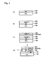
- Fig. 1(a) to (d) are cross-section drawings of a device for describing a general manufacturing method of a cell of CIGS thin film solar cell.
- Mo electrode layer 200 to be a lower electrode is formed on a substrate 100.
- a light absorbing layer 300 comprising CIGS thin film which shows p- type by controlling the composition.
- a buffer layer 400 such as CdS is formed on the light absorbing layer 300 and then a light transmitting electrode layer 500 comprising ZnO, which shows n + type by doping impurity, and is to be an upper electrode on the minus side, is formed on the buffer layer 400.
- a light transmitting electrode layer 500 comprising ZnO, which shows n + type by doping impurity, and is to be an upper electrode on the minus side
- scribe processing of from the light transmitting electrode layer 500 comprising ZnO to the Mo electrode layer 200 is collectively carried out with a mechanical scribe apparatus.
- a mechanical scribe apparatus thereby, each cell of the thin film solar cell is electrically separated, that is, each cell is individuated.
- Substances which suitably form a film by the manufacturing apparatus of the embodiment are shown below.
- n-type semiconductor forming junction with the I-III-VI compound semiconductor for example, usable is a II-VI compound such as CdS, ZnO, ZnS and Zn (O, S, OH). Those compounds can form junction surface not having recombination of the photoelectric transfer layer with carrier. For example, refer to JP-A-2002-343987 .
- a substrate for example, usable are a glass plate such as sodium lime glass, a film such as a polyimide film and a metal plate such as a stainless steel plate, a titanium plate, an aluminium plate and a copper plate.
- the above substrate for use in devices is specifically preferably film form or foil form.
- a back side electrode usable is a metal such as molybdenum, chromium and tungsten. Those metal materials are preferable because if those metal materials are heat-treated, those hardly mix with the other layer.
- the back side electrode preferably is Mo layer.
- the electrode layer preferably has a configuration in which an insulation material and metal were located in a line in the shape of a stripe (See JP-A-9-219530 ).
- material used for a transparent electrode For material used for a transparent electrode, usable are well-known materials such as ITO, ZnO:Ga, ZnO:Al, ZnO:B, and SnO 2 .
- the materials have a high light translucency, a low resistance and a high mobility of carrier, and therefore, these materials are preferable for the transparent electrode.
- the materials may be referred to JP-11-284211 .
- the layer structure examples include a super straight type and a substraight type.
- the layer structure preferably is a substright type from the viewpoint of the conversion efficiency.
- the buffer layer usable are CdS, ZnS, ZnS (O, OH) and ZnMgO.
- the window layer usable are various transparent conducting materials such as ZnO and ITO.
- the buffer layer is preferably ZnMgO, which has large energy in the conducting band.
- the buffer layer portion in the band structure of CIGS/the buffer layer/window layer (ZnO) is prevented from changing spike-like shape (convex), and therefore, the saturated current is prevented from decreasing; the layer portion is prevented from changing cliff-like shape (concave), and therefore, the open voltage and FF are prevented from decreasing; and the generating efficiency when the band gap is large is improved.
- PEN film Teijin DuPont' s trade, name, Teonex Q65FA
- PEN film Teijin DuPont' s trade, name, Teonex Q65FA
- the substrate was subjected to corona discharge treatment at 730 J/m 2 and a first layer coating solution 1 consisting of the following composition was coated on the substrate according to bar coat method.
- the coating amount was 4.4 ml/m 2 , and the coated layer was dried at 180 °C for one minute, thereby forming an easy adhesive layer having a thickness of 200 nm.
- Polyester resin binder 49.7 mass parts (manufactured by DIC Corp., FineTex ES-650, solid content 29%)
- Surfactant A 11.4 mass parts (manufactured by Sanyo Chemical Industries, Ltd., Sanded BL, solid content 10%, anion)
- Surfactant B 26.8 mass parts (manufactured by Sanyo Chemical Industries, Ltd., Naroacty NH-100, solid content 5%, nonion)
- Silica particle dispersion solution C 2.4 mass parts (AEROSIL, OX-50, 20% of aqueous dispersion solution)
- Colloidal silica dispersion solution D 4.6 mass parts (Nissan Chemical Industries, Ltd., SNOWTWX XL, 20% of aqueous dispersion solution)
- Carbodiimide compound 28.2 mass parts (manufactured by Nisshinbo Industries, Inc., Carbodilight V-02-L2, solid content 10 %, carbodiimide equivalent 385) Distil
- the coating solution consisting of the following composition was coated according to bar coat method.
- the coating amount is 5 ml/m 2
- the coated layer was cured therein through irradiation with UV light from a high-pressure mercury lamp (integrated radiation, about 2 J/cm 2 ) in a chamber having an oxygen concentration of 0.1 % after nitrogen substitution, thereby forming an organic layer having a thickness of 500 nm ⁇ 50 nm.
- Bifunctional urethane acrylic monomer 20 g (manufactured by Daicel-cytec. Com., EBECRYL 4858) UV polymerization initiator 0.6 g (manufactured by Chiba Specialchem. Com., Irgacure 907) 2-butanone 190 g
- the surface roughness of the surface of the obtained organic layer was evaluated using an atom force microscope (AFM). Then, smoothness was expressed as an average roughness Ra (unit, nm) within a sample area of 1 ⁇ m square.
- SPI3800N/SPA400 manufactured by SII NanoTechnology Inc.
- SI-DF20 as a cantilever
- an inorganic layer (aluminum oxide layer) was formed on the above organic layer.
- the target was aluminum, the discharge gas was argon and the reaction gas was oxygen.
- the pressure for forming was 0 .1 Pa and the achievement film thickness was 40 nm.
- the organic/inorganic laminate type barrier film was formed.
- the properties of the obtained barrier film (Smoothness and Water Vapor Permeability) were shown in Table 2.
- the first layer was formed in the same manner and the same prescription as Example 1. Then, on the surface, the following second layer coating solution was coated according to bar coat method. The coating amount was 4.4 ml/m 2 , and the coated layer was dried at 170 °C for one minute. Then, the laminated film on which the first layer and the second layer were coated was obtained. According to the same process as that for Example 1, for which, however, (1-2) was altered, the barrier film having a structure of the PEN substrate/the easy adhesive layer (the first layer) /the easy adhesive layer (the second layer)/the organic layer/the inorganic layer as the barrier film of Example 2 was produced.
- MMA is methylmethacrylate
- St is styrene
- 2EHA 2-ethylhexylacrylate
- HEMA hydroylmethacrylate
- AA acrylic acid
- the barrier film having a structure of the PEN substrate /the easy adhesive layer (the first layer)/the organic layer/the inorganic layer as the barrier film of Example 3 was produced.
- Acrylic resin binder 62.7 mass parts (Latex of MMA 59 -St 9 -HEMA 5 -AA 1 , concentration of solid content, 28 %) Silica particle dispersion solution C 2.7 mass parts Colloidal silica dispersion solution D 4.6 mass parts Surfactant A 9.6 mass parts Surfactant B 26.8 mass parts Carbodiimide compound added so that the addition amount relative to the binder is the amount represented in Table 1.
- MMA is methylmethacrylate
- St is styrene
- 2EHA 2-ethylhexylacrylate
- HEMA hydroylmethacrylate
- AA acrylic acid
- an organic layer was formed on the substrate prepared according to (1-1) in Example 1.
- the organic layer was formed in the same manner as that for (1-3) of Example 1, for which, however, the bifunctional urethane acrylate was placed in a mono functional acrylate (manufactured by Daicel-cytec. Com.,ODA-N).
- the barrier film of Comparative Example 1 having a structure of the PEN substrate/the organic layer/the inorganic layer was formed.
- the barrier film of Comparative Example 2 having a structure of the PEN substrate/the organic layer/the inorganic layer was formed according to the same manner as that for Comparative Example 1, for which, however, the monofunctional acrylate was placed in a bifunctional urethane acrylate (manufactured by Daicel-cytec. Com., EB4858).
- the barrier film of Comparative Example 3 having a structure of the PEN substrate/the easy adhesive layer/the organic layer/the inorganic layer was formed according to the same manner as that for Example 1, for which, however, the bifunctional urethane acrylate was placed in a bifunctional acrylate (manufactured by Daicel-cytec. Com., DPGDA).
- the barrier film of Comparative Example 4 having a structure of the PEN substrate/the easy adhesive layer (the first layer)/the easy adhesive layer (the second layer)/the organic layer/the inorganic layer was formed according to the same manner as that for Comparative Example 3, for which, however, the easy adhesive layer was altered to the same two layers constitution as that for Example 2.
- the water vapor permeability of the barrier films formed in the above Examples and Comparative Examples were determined at 40 °C and a relative humidity of 90 %, using a water vapor permeability determining apparatus (manufactured by MOCON, PERMATRAN-W3/31).
- the measurable limit is 0.005g/m 2 /day.
- the measure of the barrier films were carried out when the barrier films were not folded, the barrier films were folded in curvature radius of 20 mm (20 mmR), the barrier film were folded in curvature radius of 10 mm (10 mmR) and the barrier film were folded in curvature radius of 5 mm (5 mmR), and the results were shown in Table 1.
- the barrier films of Exemples 1 to 3 in which the center liner average roughness of the surface of the organic layer on the inorganic layer side is 0.5nm or less and the organic layer contains a resin which is obtained by curing a bifunctional urethane acrylate as a polymerizable component, expressed the high water vapor barrier property even if the barrier film is folded.
- the barrier films after being folded have much higher water vapor barrier property.
- the barrier film of Comparative Example 1 having a center liner average roughness of over 0.5 nm, the barrier film of Comparative Example 2 not having an easy adhesive layer, the barrier film of Comparative Examples 3 and 4 using the bifunctional acrylate for the organic layer in place of the bifunctional urethaneacrylate were poor in the water vapor barrier property after being folded.
- the barrier film in which the organic layer contains the resin obtained by curing the particular urethane acrylate as a polymerizable component, and the center liner average roughness of the organic layer on the inorganic layer side is 0.5 nm or less maintains the high water vapor barrier property when folded.
- lithium fluoride was vapor-deposited in a thickness of 1 nm and metal aluminium was in a thickness of 100 nm in that order, serving as a cathode.
- metal aluminium was in a thickness of 100 nm in that order, serving as a cathode.
- a silicon nitride film having a thickness of 5 ⁇ m was formed according to a parallel plate CVD method, thereby constructing an organic EL device.
- thermosetting adhesive (Daizo-Nichimori's Epotec 310)
- the device was stuck to the barrier film of Examples 1 and 2, and heated at 65 °C for 3 hours to cure the adhesive.
- 20 samples of every organic EL device were constructed.
- the organic EL devices were driven for light emission at a voltage of 7V applied thereto, using a source measure unit, Keithley's SMU2400 Model. Using a microscope, the surface of each sample was checked for its condition with light emission, and it was confirmed that all the devices gave uniform light emission with no dark spot.
- the barrier film of the invention has too much high water vapor barrier property. Further, the barrier film of the invention can maintain the high water vapor barrier property when folded. Therefore, the barrier film of the invention may be effectively used for wide uses including a flexible organic EL device.
Landscapes
- Chemical & Material Sciences (AREA)
- Organic Chemistry (AREA)
- Health & Medical Sciences (AREA)
- Chemical Kinetics & Catalysis (AREA)
- Medicinal Chemistry (AREA)
- Polymers & Plastics (AREA)
- Life Sciences & Earth Sciences (AREA)
- Engineering & Computer Science (AREA)
- Materials Engineering (AREA)
- Wood Science & Technology (AREA)
- Physics & Mathematics (AREA)
- Optics & Photonics (AREA)
- Laminated Bodies (AREA)
- Electroluminescent Light Sources (AREA)
Abstract
Description
- The present invention relates a gas-barrier laminate film (referred to as "barrier film" in the specification) usable in an electronic device material and an optical material and having a good gas-barrier property and to a method thereof.
- Heretofore, a barrier film fabricated by forming a thin metal oxide film of aluminium oxide, magnesium oxide or silicon oxide on the surface of a plastic film is widely used for wrapping or packaging articles that require shielding from various gases such as water vapor or oxygen and for wrapping or packaging edibles, industrial articles and medicines for preventing them from being deteriorated.
- Recently, in the field of liquid-crystal display devices and organic EL devices (organic electroluminescent devices), plastic films are being used in place of glass substrates that are heavy and readily cracked or broken. As applicable to a roll-to-roll system, plastic films are advantageous in point of cost. However, plastic films are problematic in that their gas-barrier property is not good as compared with that of glass substrates. Therefore, when a plastic film is used in a liquid-crystal display device, then water vapor may penetrate into the liquid-crystal cell, thereby causing display failures.
- For solving the problem, it is known to form an organic/inorganic laminate on a plastic film, thereby using the resulting barrier film.
- For example,
JP-A-2003-53881 JP-A-2003-53881 JP-A-2003-53881 -
JP-A-2005-313560 JP-A-2005-313560 -
JP-A-2005-279974 JP-A-2005-279974 JP-A-2005-279974 - However, unless the organic layer of the barrier film in
JP-A-2003-53881 JP-A-2005-313560 JP-A-2005-279974 - To solve the problems of such related arts, the present inventers have an object to provide a barrier film which maintains a high water vapor barrier property when folded.
- The present inventors have assiduously studied and, as a result, have found that the problems of the related arts can be solved by providing an easy adhesive layer between an organic layer containing a resin which is obtained by polymerizing a urethane acrylate and a plastic film, and holding a center liner average roughness low. That is, the following invention is provided as means to solve the problems.
- (1) A barrier film having a structure in which an easy adhesive layer, an organic layer and an inorganic layer are laminated in that order on one surface or both surfaces of a plastic film, wherein a center liner average roughness of a surface of the organic layer on the inorganic layer side is 0.5nm or less, and the organic layer contains a resin which is obtained by curing an acrylic monomer having at least two acryloyl groups and at least two urethane groups in one molecule as a polymerizable component.
- (2) The barrier film according to (1), wherein the easy adhesive layer contains polyester resin as a binder.
- (3) The barrier film according to (1) or (2), wherein the easy adhesive layer comprises a first layer adjacent to the substrate and a second layer on the first layer.
- (4) The barrier film according to any one of (1) to (3), wherein the easy adhesive layer comprises a first layer adjacent to the substrate and a second layer on the first layer, the first layer contains a polyester resin as a binder, and the second layer contains an acrylic resin or a urethane resin as a binder.
- (5) The barrier film according to any one of (1) to (4), wherein the easy adhesive layer contains a carbodiimide compound.
- (6) The barrier film according to any one of (1) to (5), wherein the barrier film after folded in curvature radius of 5 mm has a water vapor permeability of at 0.01 g/m2·day or less.
- (7) The barrier film according to any one of (1) to (6), wherein the acrylic monomer is represented by the following formula (1):
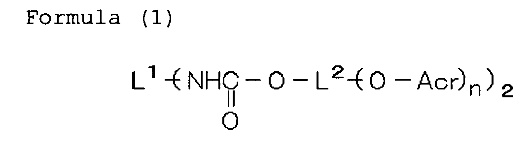
- (8) The barrier film according to any one of (1) to (7), wherein the acrylic monomer is represented by the following formula (1):

L1 is selected from


- (9) The barrier film according to any one of (1) to (8), wherein the polymerizable component of the organic layer further contains a monofunctional monomer.
- (10) The barrier film according to any one of (1) to (9), wherein the organic layer has a thickness of 50 to 5000 nm.
- (11) The barrier film according to any one of (1) to (10), wherein the inorganic layer has a thickness of 10 to 300 nm.
- (12) An device comprising a barrier film according to any one of (1) to (11).
- (13) An organic EL device comprising a barrier film according to any one of (1) to (11).
- The barrier film of the invention makes it possible to maintain a high water vapor barrier property even if the barrier film is folded. The device of the invention has a high permanence.
-
-
Fig. 1 shows a cross-section drawing of a general device of a cell of a CIGS solar cell. - The barrier film and the device of the invention are described in detail hereinunder. The description made hereinunder is for some typical embodiments of the invention, to which, however, the invention should not be limited. In this description, the numerical range expressed by the wording "a number to another number" means the range that falls between the former number indicating the lowermost limit of the range and the latter number indicating the uppermost limit thereof.
- The barrier film of the invention is characterized in that it has a structure in which an easy adhesive layer, an organic layer and an inorganic layer are laminated in that order on one surface or both surfaces of a plastic film, and a center liner average roughness of the surface of the organic layer on the inorganic layer side is 0.5nm or less, and the organic layer contains a resin which is obtained by curing an acrylic monomer having at least two acryloyl groups and at least two urethane groups in one molecule as a polymerizable component.
- In the barrier film of the invention, the substrate film is generally a plastic film. Not specifically defined in point of the material and the thickness thereof, the plastic film usable herein may be any one capable of supporting a laminate of an easy adhesive layer, an organic layer and an inorganic layer; and it may be suitably selected depending on the use and the object thereof. Concretely, the plastic film includes metal supports (e.g., aluminium, copper, stainless), and thermoplastic resins such as polyester resin, methacryl resin, methacrylic acid-maleic anhydride copolymer, polystyrene resin, transparent fluororesin, polyimide, fluoropolyimide resin, polyamide resin, polyamidimide resin, polyetherimide resin, cellulose acylate resin, polyurethane resin, polyether ether ketone resin, polycarbonate resin, alicyclic polyolefin resin, polyarylate resin, polyether sulfone resin, polysulfone resin, cycloolefin copolymer, fluorene ring-modified polycarbonate resin, alicyclic-modified polycarbonate resin, fluorene ring-modified polyester resin, acryloyl compound.
- In case where the barrier film of the invention is used as a substrate of a device such as an organic EL device to be mentioned hereinunder, it is desirable that the plastic film is formed of a heat-resistant material. Concretely, the plastic film is preferably formed of a heat-resistant transparent material having a glass transition temperature (Tg) of not lower than 100°C and/or a linear thermal expansion coefficient of at least 40 ppm/°C. Tg and the linear expansion coefficient may be controlled by the additives to the material. The thermoplastic resin of the type includes, for example, polyethylene naphthalate (PEN: 120°C), polycarbonate (PC: 140°C), alicyclic polyolefin (e.g., Nippon Zeon's Zeonoa 1600: 160°C), polyarylate (PAr: 210°C), polyether sulfone (PES: 220°C), polysulfone (PSF: 190°C), cycloolefin copolymer (COC, compound described in
JP-A 2001-150584 JP-A 2000-227603 JP-A 2000-227603 JP-A 2002-80616 - When the barrier film of the invention is used as combined with a polarizing plate, a barrier layer side of the barrier film, in which the barrier layer side is a side of which a laminate comprising at least one inorganic layer and at least one organic layer is formed, is directed at the inside of the cell; and the barrier film is preferably provided on the innermost side of the cell, that is, the barrier film is preferably adjacent to the device. In such a case, a retardation value is important, because the barrier film is provided in the inside of the cell inner than the polarizing plate. In such embodiment, it is preferable that a barrier film comprising a substrate having a retardation value of 10 nm or less is laminated on a circular polarizing plate (1/4 wavelength plate + (1/2 wavelength plate) + liner polarizing plate) or that a barrier film comprising a substrate applicable as a 1/4 wavelength plate and having a retardation value of 100 nm to 180 nm is combined with a linear polarizing plate.
- The substrate having a retardation value of 10 nm or less include a cellulose triacetate (Fuji Film, Fuji TAC), polycarbonate (Teijin Chemicals Ltd., Pureace; Kaneka, ELMECH), cycloolefin polymer (JSR Corp., ARTON; ZEON Corp., ZEONOR), cycloolefin copolymer (Mitsui Chem. Inc., APEL (pellet); Polyplastic Com.,TOPAS), polyallylate (Unitika, U100 (pellet)), transparent polyimide (Mitsubishi Gas Chem. Inc., Neoprium).
- As a 1/4 wavelength plate, usable is a film which was adjusted to a desired retardation by stretching the above film.
- Since the barrier film of the invention is usable in devices such as organic EL devices, the plastic film is transparent, or that is, its light transmittance is generally at least 80%, preferably at least 85%, more preferably at least 90%. The light transmittance may be measured according to the method described in JIS-K7105.
- Concretely, using an integrating sphere-type light transmittance meter, a whole light transmittance and a quantity of scattered light are measured, and the diffusive transmittance is subtracted from the whole transmittance to obtain the intended light transmittance of the sample.
- Even when the barrier film of the invention is used in displays, it does not always require transparency in a case where it is not disposed on the viewers' side. Accordingly in such a case, a nontransparent material may be used for the plastic film. The nontransparent material includes, for example, polyimide, polyacrylonitrile, known liquid-crystal polymer.
- Not specifically defined, the thickness of the plastic film for use in the barrier film of the invention may be suitably selected depending on its use. Typically, the thickness may be from 1 to 800 µm, preferably from 10 to 200 µm. The plastic film may have a functional layer such as a transparent conductive layer, a primer layer, etc. The functional layer is described in detail in
JP-A 2006-289627 - In the invention, an easy adhesive layer may have a single layer constitution or a two layers constitution. The single layer constitution achieves satisfying adhesiveness, and however, the two layers constitution achieves stronger adhesiveness to improve the folding resistance.
- When an easy adhesive layer of the invention is a single layer constitution, then the layer is directly laminated on a plastic film. The layer is necessary to contain a binder and preferably contains a carbodiimide crosslinking agent, which is described in the easy adhesive structure having a two layers constitution. The layer further may include matting agent, surfactant, antistatic addictive and particles for controlling flexibility, if necessary.
- The binder of the easy adhesive layer having a single layer constitution of the invention is not defined, and however, usable are an acrylic resin, a polyurethane resin, a polyester resin and a rubber resin.
- The acrylic resin is a polymer composed of an acrylic acid, a methacrylic acid or a derivatives thereof. Specifically, examples of the acrylic resin include a polymer which is obtained by copolymerizing acrylic acid, methacrylic acid, methylmethacrylate, ethylacrylate, butylacrylate, 2-ethylhexylacrylate, acrylamide, acrylonitrile, hydroxylacrylate and the like, as a main component, with a monomer copolymerizable therewith, for example, styrene and divinylbenzene.
- The polyurethane resin is a generic term of a polymer having a urethane bonding in the main chain, generally obtained by reacting polyisocyanate with polyol.
- Examples of the polyisocyanate include TDI, MDI, NDI TODI, HDI and IPDI and examples of the polyol include ethylene glycol, propylene glycol, glycerin and hexane triol. Furthermore, in the invention, usable is the polymer which is obtained by subjecting a urethane polymer obtained by reacting polyisocyanate with polyol to chain elongation treatment, thereby increasing the molecular weight thereof. The polyisocyanate, polyol and chain elongation treatment, as described above, for example, are described in "Polyurethane Resin Hand Book" which was edited by IWATA Keizi and issued by Nikkan Kogyo Shimbun on 1987.
- The polyester resin is a generic term of a polymer having an ester bonding in the main chain, generally obtained by reacting polycarboxylic acid and polyol. Examples of the polycarboxylic acid include fumaric acid, itaconic acid, adipic acid, sebacic acid, terephthalic acid and isophthalic acid and examples of the polyol include the above examples thereof. The polyester resin and the material thereof are, for example, described in "Polyester Resin Hand Book" which was edited by TAKIYAMA Eiichiro and issued by Nikkan Kogyo Shimbun on 1988.
- The rubber resin of the invention is a diene synthetic rubber among syhthetic rubbers. Specific examples include polybutadiene, styrene-butadiene copolymer, styrene-butadiene-acrylonitrile copolymer, styrene-butadiene-divinylbenzene copolymer, butadiene-acrylonitrile copolymer, polychloroprene. The rubber resin of the invention is, for example, described in "Synthesis Rubber Hand Book" which is edited by KANBARA Syu et al. and issued by Asakura Syoten on 1967.
- Specifically preferably, the binder of the easy adhesive layer having a single layer constitution of the invention is polyester resin from the view point of adhesiveness with a polyester substrate.
- Specifically preferably, the polymer of the binder of the easy adhesive layer having a single layer constitution of the invention is a polymer having a carboxyl group on the molecule among the above-mentioned polymers.
- When the binder of the easy adhesive polymer of the single layer constitution of the invention is used, the above polymer may be dissolved in an organic solvent or be used as aqueous dispersion. Since environment impact is small, the binder is preferably coated by aqueous type coating using aqueous dispersion. For the aqueous dispersion, usable are commercially available polymers as follows: Super Flex 830, 460, 870, 420 420NS (polyurethane manufactured by Dai-ichi Kogyo Seiyaku Co., Ltd.), VONDIC 1370NS, 1320NS, HW APX-101H, AP40(F) (polyurethane manufactured by DIC Corp.), Jurymer ET325, ET410, SEK301 (acrylic manufactured by Nihon Junyaku Co.,Ltd.), Boncoat AN117, AN226 (acrylic manufactured by DIC Corp.), Luxter DS616, DS807 (styrene-butadiene rubber manufactured by DIC Corp.), Nippor LX110, LX206, LX426, LX433 (styrene-butadiene rubber manufactured by ZEON Corp.), Nippor LX513, LX1551, LX550, LX1571 (acrylic nitrile-butadiene rubber manufactured by ZEON Corp.), FineTex Es650,Es2200 (polyester manufactured by DIC Corp.), Vylonal MD1400, MD1480 (polyester manufactured by Toyobo).
- For the polymer used as the binder of the easy adhesive layer having a single layer constitution of the invention, one or more different types thereof may be ether singly or as combined.
- The molecular weight of the polymer used as the binder of the easy adhesive layer having a single layer constitution of the invention is not specifically defined, and generally, preferred is weight-average molecular weight of 3,000 to 1,000,000. When the weight-average molecular is 3,000 or more, then strength of the coating layer tends to be higher, and when the weight-average molecular weight is 1,000,000 or less, then the surface of the coating tends to be better.
- The easy adhesive layer having a single layer constitution of the invention preferably contains the after-mentioned carbodiimide crosslinking agent. The carbodiimide crosslinking agent preferably contains 1 to 100 % by mass relative to the binder of the easy adhesive layer having a single layer constitution, more preferably 5 to 50 % by mass. When the addition amount is 1 % by mass or more, then falling of particles from the layer to be formed tends to be sufficiently prevented. When the addition amount is 100 % by mass or less, then the surface to be coated tends to be better.
- The matting agent usable in the easy adhesive layer having a single layer constitution of the invention is preferably either of organic particles and inorganic particles. For example, polymer particles such as polystyrene, polymethylmethacrylate, silicone resin, benzoguanamine resin and inorganic particles such as silica, calcium carbonate, magnesium oxide, magnesium carbonate may be used. Of those, polystyrenem, polymethylmethacrylate and silica are preferable from the viewpoints of improvement of the slipping property and the cost thereof.
- The average particle diameter of the matting agent for use in the invention is preferably 0.3 to 12 µm, more preferably 0.5 to 9µm. When the average particle diameter is 0.3 or more, then the slipping property tends to be more sufficient. When the average particle diameter is 12 µm or less, then the device to be formed tends to excel in display appearance quality.
- Depending on the average particle diameter, the addition amount of the matting agent of the invention is preferably 0.1 to 30 mg/m2, more preferably 0.5 to 20 mg/m2. When the addition amount thereof is 0.1 mg/m2 or more, then the easy adhesive layer to be formed tends to be improved in slipping property. When the addition amount thereof is 30 mg/m2 or less, then the device to be formed tends to excel in display appearance quality.
- The surfactant usable in the easy adhesive layer having a single layer constitution of the invention is well-known anion, nonion and cation surfactants. The surfactant is, for example, described in "Surfactant Handbook" which was edited by NISHI Ichiro, IMAI Tooziro and KASAI Masai and was issued by Sangyo Tosyo Co, Ltd. on 1960. The addition amount of the surfactant is preferable 0.1 to 30 mg/m2, more preferable 0.2 to 10 mg/m2. When the addition amount is 0.1 mg/m2 or more, occurrence of cissing tends to be inhibited. When the addition amount is 30 mg/m2 or less, then the surface to be coated tends to be better.
- When the easy adhesive layer having a single layer constitution of the invention is needed to control flexibility, the easy adhesive layer contains particles, for example, particles primarily consisting tin dioxide, zirconia and titanium oxide. Also, the titanium chelate compounds described in
JP-A-2005-97571 - The tin dioxide is preferably a tin dioxide (IV) having a composition of SnO2. Specifically preferred is a tin dioxide doping stibium since tin dioxide has conductibility and surface resistance of the laminate film to be formed is lowered, and therefore, preventing dust from adhering. For such tin dioxide particles, usable are commercially available particles such as FS-10D, SN-38F, SN-100F, TDL-S and TDL-1 (all is stibium doped-tin dioxide particles manufactured by Ishihara Sangyo Kaisha Ltd.).
- The zirconia has a composition of ZrO2 and, for example, usable are NZS-20A and NZS-30A(either is manufactured by Nissan Chemical Industries, Ltd.)
- The titanium oxide is preferably a titanium oxide (IV) having a composition of TiO2. The titanium oxide may be a rutile type or an atanase type. Also, the surface thereof may be treated. For the titanium oxide, for example, usable are Idemitsu titania IT-S, IT-O and IT-W (all is manufactured by Idemitsu).
- The antistatic additive usable in the easy adhesive layer having a single layer constitution of the invention includes an electronic conductive polymer such as polyaniline and polypyrrole, an ion conductive polymer having a carboxyl group or a surfonic acid group in the molecular chain and a conductive particle. Of those, the above-mentioned stibium doped-tin dioxide is specifically preferable from the viewpoints of conductivity and transparency. For the addition amount of the antistatic additive, it is preferably added so that surface resistance of the easy adhesive layer which is measured at 25 °C, relative humidity of 30 % is in the range of 1 × 10⁵ to 1 x 10¹³. When the surface resistance is 1 x 10⁵ or more, the laminate film to be formed tends to avoid degradation of transparency depending on increase of the addition amount of the antistatic additive. When the surface resistance is 1 x 10¹³ or less, disadvantages such as adhesion of dust does not tend to occur.
- The thickness of the easy adhesive layer having a single layer constitution of the invention is preferably 10 to 500 nm, more preferably 30 to 150 nm. When the thickness thereof is 10 nm or more, then the easy adhesive layer tends to be better in its adhesiveness to the adjacent polyester substrate. When the thickness thereof is 500 nm or less, the surface of the easy adhesive layer tends to be better.
- The method of coating of the easy adhesive layer having a single layer constitution of the invention is not specifically limited, usable are well-know methods such as bar-coator coating and slide-coator coating. For the coating solvent, usable is either of aqueous type and organic type solvents such as water, toluene, methanol, isopropyl alcohol, methyl ethyl ketone and a mixture thereof. Of those, the method using water as the coating solvent is preferable in view of easiness of the manufacture.
- Then, the adhesive layer having a two layers constitution is described. The layer closer to the substrate of the two layers constitution (first layer) is the same as the above-mentioned the easy adhesive layer having a single layer constitution. The second layer of the invention is coated on a position away from the polyester substrate than the first layer. The layer may contain a matting agent, a slipping agent, a surfactant, an antistatic addictive and particles for controlling flexibility in addition to a binder and a crosslinking agent, if necessary.
- For the binder of the second layer of the invention, usable are an acrylic resin and a urethane resin. The polymer used as the binder is more preferably a polymer having a carboxyl group in the molecule. For the acrylic resin and urethane resin, usable are what are described in the easy adhesive layer having a single layer constitution.
- When the binder of the second layer of the invention is used, the above polymer may be resolved in an organic solvent or may be used as aqueous dispersion. Since environment impact is small, the binder is preferably coated by aqueous type coating using aqueous dispersion. For the aqueous dispersion, usable are the above-mentioned commercially available polymers.
- One or more different types of the polymer used as a binder of the second layer of the invention may be used herein either singly or as combined, if necessary.
- The molecular weight of the polymer used as the binder of the easy adhesive layer having a single layer constitution of the invention is not specifically defined, generally, preferred is weight-average molecular weight of 3,000 to 1,000,000. When the weight-average molecular is 3,000 or more, then strength of the coating layer tends to be higher, and when the weight-average molecular weight is 1,000,000 or less, then the surface of the coating tends to be better.
- The crosslinking agent applicable to the second layer of the invention is not specifically defined, preferred is a carbodiimide or epoxy crosslinking agent.
- The carbodiimide crosslinking agent for use in the invention (hereinafter, sometimes reffered to as carbodiimide compound) is not particularly limited herein as long as the compound is a compound having a carbodiimide group in the molecule. The carbodiimide compound is generally synthesized through condensation reaction. Herein, an organic group of an organic diisocyanate usable in the synthesis of the carbodiimide compound is not particularly limited, usable is either of an aromatic type, an aliphatic type and a mixture thereof, and preferred is an aliphatic type from the viewpoint of the reactivity. The carbodiimide crosslinking agent usable in the invention is available as a commertical available such as carbodiright V-02-L2 (manufactured by Nisshinbo Industries, Inc.).
- The "epoxy crosslinking agent" is not particularly limited as long as it has a compound having two epoxy groups in the molecule. Examples of the epoxy crosslinking agent include Dinacol, EX614B, EX521, EX512, EX301, EX313, EX314, EX810, EX811.
- The crosslinking agent of the invention is preferably added in the range of 1 to 100 % by mass relative to the binder, more preferably 5 to 50 % by mass. When the addition amount is 1 % by mass or more, it tends to improve its adhesiveness to the adjacent layer. When the addition amount is 100 % by mass or less, then the surface of the coating tends to be better.
- The matting agent, surfactant, antistatic additive, particles for controlling flexibility usable in the second layer of the invention are the same as those of the above-mentioned easy adhesive layer having a single layer constitution.
- The thickness of the second layer of the invention is not particularly limited, preferably 10 to 5,000 nm, more preferably 20 to 1500 nm. When the thickness thereof is 10 nm or more, it tends to improve its adhesiveness to the adjacent layer. When the thickness thereof is 5,000 nm or less, the surface thereof tends to be better.
- The coating method of the second layer is not particularly limited, usable are well-know methods such as bar-coator coating and slide-coator. The second layer of the invention may be coated by the same methods as or different methods from that for the easy adhesive layer having a single layer constitution. Furthermore, the second layer of the invention may be coated to dry at the same time with the easy adhesive layer having a single layer constitution or be coated after the easy adhesive layer having a single layer constitution is coated to dry.
- For the coating solvent for coating the second layer of the invention, usable is either of aqueous type and organic type solvents such as water, toluene, methanol, isopropyl alcohol, methyl ethyl ketone and a mixture thereof. The coating solvent may be the same as or different from that of the first layer. The solvent of the second layer of the invention is also preferably water from the viewpoints of the easiness of manufacturing and the cost thereof.
- The organic layer contains a resin which is obtained by curing an acrylic monomer having at least two (meth)acryloyl groups and at least two urethane groups in the molecule (hereinafter, referred to as the acrylic monomer of the invention) as a polymerizable component. Examples of the acrylic monomer of the invention include a monomer having a structure represented by the following Formula (1).

- In the Formula (1), Acr is an acryloyl group or a methacryloyl group, n is an integer of 1, to 5, L1 is a bivalent linking group and L2 is a linking group having valence of (n + 1).
- Examples of L1 include a liner alkylene group, an alicyclic alkylene group, an arylene group and an aralkylene group. Specific examples of L1 are shown below, to which, however, L1 for use in the invention should not be limited.

- Examples of L2 include a liner alkylene group or a trivalent to hexatomic group obtained by removing voluntary 1 to 4 of hydrogen atom from the liner alkylene group. Specific examples of L2 are shown below, to which, however, L2 for use in the invention should not be limited.


- Of the monomer represented by the Formula (1), preferred is an acrylic monomer having from two to six functional groups.
- Specific examples of the acrylic monomer for use in the invention are shown below, to which, however, the acrylic monomer for use in the invention should not be limited. L2s may be the same or differ to each other in the Formula (1).


- The acrylic monomer of the invention preferably has a molecular weight of 100 to 5000, more preferably 200 to 2000, furthermore preferably 300 to 1000. One or more different types of the acrylic monomer of the invention may be used singly or as combined.
- In the organic layer of the barrier firm of the invention, a resin which is obtained by polymerizing only the acrylic monomer of the invention may be used, however, preferably a resin which is obtained by copolymerizing the acrylic monomer of the invention with a monomer other than that. Examples of a monomer copolymerizable with the acrylic monomer of the invention includes an acrylic monomer other than the acrylic monomer of the invention, styrene monomer, vinylester polymer, acrylamide monomer, maleic acid monomer. The monomer copolymerizable with the acrylic monomer of the invention is preferably a monofunctional monomer, more preferably a monofunctional acrylic monomer and a monofunctional methacrylic monomer. The molecular weight for the monofunctional acrylic monomer and the monofunctional methacrylic monomer is not specifically limited, generally, 150 to 600. One or more different monomers copolymerizing may be used singly or as combined. Specific examples of the monofunctional monomer is shown below, to which, however, the monofunctional monomer for use in the invention should not be limited.


- The molar ratio of the acrylic monomer of the invention to the monomer other than that of the invention is not specifically limited. The molar ratio is preferably 0 to 20 mole of the monomer other than the monomer of the invention relative to one mole of the acrylic monomer of the invention, more preferably 0 to 10 mole, furthermore preferably 0 to 5 mole.
- A monomer mixture of the acrylic monomer of the invention and the monomer other than the monomer of the invention may contain a phosphoric acid system (meth)acrylate monomer or a (meth)acrylate monomer having a silancoupling group for the viewpoints of improvement of adhesiveness.
- Examples of the phosphoric acid system (meth) acrylate monomer or the (meth) acrylate monomer having a silancoupling group are shown below, to which, the invention is not limited.


- For forming the organic layer, usable are ordinary solution coating method and vacuum film formation method. The solution coating method includes, for example, a dip coating method, an air knife coating method, a curtain coating method, a roller coating method, a wire bar coating method, a gravure coating method, a slide coating method, and an extrusion coating method of using a hopper as in
USP 2,681,294 . Not specifically defined, the vacuum film formation method is preferably a flash vacuum evaporation method as inUSP 4,842,893 ,4,954,371 ,5,032,461 . - The monomer polymerization method is not specifically defined, for which, for example, preferred is thermal polymerization, light (UV, visible ray) polymerization, electronic beam polymerization, plasma polymerization or their combination. Of those, especially preferred is photopolymerization. In photopolymerization, a photopolymerization initiator may be used. Examples of the photopolymerization initiator are Irgacure series (e.g., Irgacure 651, Irgacure 754, Irgacure 184, Irgacure 2959, Irgacure 907, Irgacure 369, Irgacure 379, Irgacure 819) sold by Ciba Specialty Chemicals; Darocure series (e.g., Darocure TPO, Darocure 1173); Quantacure PDO; Esacure series (e.g., Esacure TZM, Esacure TZT) and oligomer-type Esacure KIP series sold by Sartomer.
- The light for irradiation is generally UV light from high-pressure mercy lamp or low-pressure mercy lamp. The irradiation energy is preferably at least 0.5 J/cm2, more preferably at least 2 J/cm2. In case where the oxygen concentration in polymerization is lowered by a nitrogen substitution method, the oxygen concentration is preferably at most 2%, more preferably at most 0.5%. In case where the oxygen partial pressure in polymerization is lowered by a pressure reduction method, the total pressure is preferably at most 1000 Pa, more preferably at most 100 Pa. Especially preferred is UV polymerization with energy irradiation of at least 2 J/cm2 under a reduced pressure condition of at most 100 Pa. The polymerization of the monomer is preferably carried out after the monomer mixture is provided on the plastic film, for example, by coating.
- The center liner average roughness of the organic layer on the side of the inorganic layer is preferably 0.5 nm or less, more preferably 0.4 nm or less, even more preferably 0.3 nm or less.
- The thickness of the organic layer is not specifically defined. However, when too thin, the layer could not be uniform; but when too thick, the layer may be cracked and its barrier capability may lower. From these viewpoints, the thickness of the organic layer is preferably from 50 nm to 5000 nm, more preferably from 200 nm to 2000 nm.
- Since the barrier film of the invention has a structure in which the organic layer containing a resin obtained by curing an acrylic monomer having urethane groups as a polymerizalbe component is laminated on the easy adhesive layer, the adhesiveness of the organic layer to the easy adhesive layer is improved and the organic layer is not easily peeled even if the barrier film is folded. Accordingly, the barrier film of the invention has the high vapor barrier property and can maintain such the high barrier property even if the barrier film is folded.
- The inorganic layer is, in general, a layer of a thin film comprising a metal compound. For forming the inorganic layer, usable is any method capable of producing the intended thin film. For it, for example, suitable are physical vapor deposition methods (PVD) such as a vapor evaporation method, a sputtering method, an ion plating method; various chemical vapor deposition methods (CVD); liquid phase growth methods such as a plating or sol-gel method. Of those, preferred are physical vapor deposition methods (PVD) and chemical vapor deposition methods (CVD), which may evade thermal influences on the substrate film in inorganic layer formation, and which may readily produce uniform thin film layers at rapid production speed. Not specifically defined, the component to be in the inorganic layer may be any one satisfies the above-mentioned requirements. For example, it includes oxides, nitrides or oxinitrides containing at least one metal selected from Si, Al, In, Sn, Zn, Ti, Cu, Ce and Ta. Of those, preferred are oxides, nitrides or oxinitrides of a metal selected from Si, Al, In, Sn, Zn and Ti; more preferred are metal oxides, nitrides or oxinitrides with Si or Al. These may contain any other element as a subsidiary component.
- In the invention, the inorganic layer is formed on the organic layer which has a smooth surface and, therefore, the inorganic layer to be formed has a surface of which smoothness is high. The smoothness of the inorganic layer to be formed in the invention is preferably 0.5 nm or less at terms of the mean roughness (Ra value) in 10 µm square, more preferably 0.3 nm or less, even more preferably 0.1 nm or less.
- Not specifically defined, the thickness of the inorganic layer is preferably within the range of from 10 to 300 nm per layer, more preferably 10 to 200 nm, even more preferably 20 to 100 nm and furthermore preferably 30 to 70 nm.
- Two or more of the inorganic layers may be laminated. In this case, for each layer, one or different types compositions are used singly or as combined. When the two or more layers are laminated, it is desirable that each inorganic layer is designed in the above preferable range.
- The barrier film may have any layer on the inorganic layer as long as the barrier film has a structure in which the easy adhesive layer, the organic layer and the inorganic layer are laminated in that order. Preferable examples of the structure include a structure in which organic layers and inorganic layers are alternately on the inorganic layer. The outermost layer may be an inorganic layer or an organic layer.
- The organic layer and the inorganic layer may be laminated by repeated film formation to form the organic layer and the inorganic layer in a desired layer constitution. In case where the inorganic layer is formed according to a vacuum film formation method such as sputtering method, vacuum evaporation method, ion plating method or plasma CVD method, then it is desirable that the organic layer is also formed according to a vacuum film formation method such as the above-mentioned flash vapor deposition method. While the barrier layer is formed, it is especially desirable that the organic layer and the inorganic layer are laminated all the time in a vacuum of at most 1000 Pa, not restoring the pressure to an atmospheric pressure during the film formation. More preferably, the pressure is at most 100 Pa, even more preferably at most 50 Pa, still more preferably at most 20 Pa.
- The barrier film of the invention is favorably used for a substrate and a sealing film of various devices. For example, the barrier film may be used for a substrate or a sealing film of organic EL devices and solar cells. Herein, the barrier film preferably seals the device so that the easy adhesive layer side is closer to the device. The barrier film may be provided on the both side or one side of the device. Examples of the display device in the invention include circular polarizing plates, liquid-crystal display devices, touch panels and organic EL devices. For solar cell devices for use in the invention, what are generally used for solar cell devices is used. Examples include single crystal silicon solar cell devices, polycrystalline silicon solar cell devices, amorphous silicon solar cell devices which are constructed in a single junction type or a tandem structure type, III-V compound semiconductor solar cell devices such as a gallium arsenide (GaAs) semiconductor solar cell device and an indium phosphorus (InP) semiconductor solar cell device, II-VI compound semiconductor solar cell devices such as a cadmium tellurium (CdTe) semiconductor solar cell device, I-III-VI compound semiconductor solar cell device such as a copper/indium/selenium (CIS) semiconductor solar cell device, a copper/indium/gallium/selenium (CIGS) semiconductor solar cell device and a copper/indium/gallium /selenium/sulfur (CIGSS) semiconductor solar cell device, dye sensitizing solar cell devices and organic solar cell devices. Of those, the solar cell device of the invention is I-III-VI compound semiconductor solar cell devices such as a copper/indium/selenium (CIS) semiconductor solar cell device, a copper/indium/gallium/selenium (CIGS) semiconductor solar cell device and a copper/indium/gallium/selenium/sulfur (CIGSS) semiconductor solar cell device.
- The barrier film of the invention can be preferably used as an organic EL devise. Here, an organic EL device using a barrier film of the invention (hereinafter referred to as organic EL devise of the invention).
- The organic EL device of the invention has a cathode and an anode on a substrate and has an organic compound layer containing an organic light emitting layer (hereinafter sometimes simply referred to as "light emitting layer") between both of the electrodes. In view of the property of the light emitting device, at least one of the anode and the cathode is preferably transparent.
- As the form of the lamination of the organic compound layer in the invention, it is preferred such a form that a hole transporting layer, a light emitting layer, and an electron transporting layer are laminated in this order from the side of the anode. Further, a charge blocking layer or the like may be present between the hole transporting layer and the light emitting layer or between the light emitting layer and the electron transporting layer. A hole injecting layer may be provided between the anode and the hole transporting layer and an electron injecting layer may be present between the cathode and the electron transporting layer. Each of the layers may be divided into a plurality of secondary layers.
- It may usually suffice that the anode has a function as an electrode for supplying holes to the organic compound layer and the shape, structure, size, etc. thereof are not particularly limited and can be selected properly from known electrode materials in accordance with the application use and the purpose of the light emitting device. As described above, the anode is formed usually as a transparent anode.
- The material for the anode includes preferably, for example, metals, alloys, metal oxides, conductive compounds or mixtures of them. Specific examples of the anode material include conductive metal oxides such as tin oxide doped with antimony, fluorine, etc. (ATO, FTO), tin oxide, zinc oxide, indium oxide, indium tin oxide (ITO), and indium zinc oxide (IZO), metals such as gold, silver, chromium, and nickel, as well as mixtures or laminates of such metals with conductive metal oxides, inorganic conductive materials such as copper iodide, and copper sulfide, organic conductive materials such as polyaniline, polythiophene and polypyrrole, and laminates thereof with ITO. Among them, preferred are conductive metal oxides, and ITO is particularly preferred with a view point of productivity, high conductivity, transparency, etc.
- The anode can be formed on the substrate in accordance with a method selected properly, for example, from wet method such as a printing method and a coating method, physical method such as a vacuum vapor deposition method, a sputtering method, and an ion plating method, and chemical method such as CVD or plasma CVD while considering the adaptability with the material constituting the anode. For example, in a case of selecting ITO as the material for the anode, the anode can be formed in accordance with a DC or RF sputtering method, a vacuum deposition method, an ion plating method, etc.
- In the organic EL device of the invention, the position for forming the anode is not particularly limited and can be selected properly in accordance with the application use and the purpose of the light emitting device and it is preferably formed on the substrate. In this case, the anode may be formed entirely or partially on one of the surfaces of the substrate.
- Patterning upon forming the anode may be conducted by chemical etching adopting photolithography, etc., or by physical etching adopting laser, etc. Further, the patterning may be conducted by vapor deposition, sputtering, etc. while stacking a mask, or by a lift-off method or a printing method.
- The thickness of the anode can be selected properly depending on the material constituting the anode and, while it can not be determined generally, it is usually about from 10 nm to 50 µm and, preferably, from 50 nm to 20 µm.
- The resistance value of the anode is, preferably, 103 Ω/□ or less and, more preferably, 102 Ω/□ or less. In a case where the anode is transparent, it may be colorless transparent or colored transparent. For taking out light emission from the side of the transparent anode, the transmittance is, preferably, 60% or higher and, more preferably, 70% or higher.
- The transparent anode is described specifically in "New Development of Transparent Electrode Film", supervised by Yutaka Sawada, published from CMC (1999) and the matters described therein can be applied to the invention. In a case of using a plastic substrate of low heat resistance, a transparent anode using ITO or IZO and formed as a film at a low temperature of 150°C or lower is preferred.
- It may usually suffice that the cathode has a function as an electrode for injecting electrons to the organic compound layer, and the shape, structure, size, etc. thereof are not particularly limited and can be selected properly from known electrode materials in accordance with the application use and the purpose of the light emitting device.
- The material constituting the cathode includes, for example, metals, alloys, metal oxides, electroconductive compounds, and mixtures thereof. Specific examples include alkali metals (for example, Li, Na, K, and Cs), alkali earth metals (for example, Mg and Ca), gold, silver, lead, aluminum, sodium-potassium alloy, lithium-aluminum alloy, magnesium-silver alloy, indium, and rare earth metals such as ytterbium. They may be used alone or two or more of them can be preferably used in combination with a view point of making the stability and the electron injecting property compatible.
- Among them, as the material constituting the cathode, alkali metals or alkali earth metals are preferred in view of the electron injecting property and materials mainly comprising aluminum are preferred with a view point of excellent storage stability.
- Materials mainly comprising aluminum mean aluminum per se, alloys of aluminum and from 0.01 to 10 mass% of alkali metals or alkali earth metals, or mixtures thereof (for example, lithium-aluminum alloy, and magnesium-aluminum alloy).
- The materials for the cathode are described specifically in
JP-A-2-15595 JP-A-5-121172 - The method of forming the cathode is not particularly limited and it can be conducted in accordance with known methods. For example, the cathode can be formed in accordance with a method selected properly from wetting methods such as a printing method and a coating method, physical methods such as a vacuum vapor deposition method, a sputtering method or, an ion plating method, and chemical methods such as a CVD or plasma CVD method while considering the adaptability with the material constituting the cathode. For example, in a case of selecting metals or the like as a material for the cathode, it can be formed in accordance with a sputtering method, etc. by sputtering one of them or plurality of them simultaneously or successively.
- Patterning upon forming the cathode may be conducted by chemical etching such as photolithography, or physical etching such as by laser, or it may be conducted by vacuum vapor deposition or sputtering while stacking a mask or by a lift off method or a printing method.
- In the invention, the position for forming the cathode is not particularly limited and it may be formed entirely or partially on the organic compound layer.
- Further, a dielectric layer of a fluoride or oxide of an alkali metal or alkali earth metal may be inserted at a thickness of from 0.1 to 5 nm between the cathode and the organic compound layer. The dielectric layer can be regarded as a sort of an electron injecting layer. The dielectric layer can be formed, for example, by a vacuum vapor deposition method, a sputtering method or an ion plating method.
- The thickness of the cathode can be selected properly depending on the material constituting the cathode and, while it can not be defined generally, it is usually about from 10 nm to 5 µm and, preferably, from 50 nm to 1 µm.
- The cathode may be transparent or not transparent. The transparent cathode can be formed by forming a thin film of the material of the cathode to a thickness of from 1 to 10 nm and, further, laminating a transparent conductive material such as ITO or IZO.
- The organic compound layer in the invention is to be described.
- The organic EL device of the invention has at least one organic compound layer containing at least a light emitting layer. Other organic compound layers than the organic light emitting layer include layers such as a hole transporting layer, an electron transporting layer, a charge blocking layer, a hole injecting layer, and an electron injecting layer respectively as described above.
- In the organic EL device of the invention, each of the layers constituting the organic compound layer can be formed suitably by any of dry film forming methods such as a vapor deposition method or a sputtering method, a transfer method, a printing method, etc.
- The organic light emitting layer is a layer having a function of accepting holes from the anode, the hole injecting layer, or the hole transporting layer and accepting electrons from the cathode, the electron injecting layer, or the electron transporting layer upon application of an electric field, and providing a site for re-combination of hole and electron to emit light.
- The light emitting layer in the invention may be formed only of a light emitting material, or may be formed of a mixture of a host material and light emitting material. The light emitting material may be a fluorescent material or a phosphorescent material, and the dopant may be of one or plural kinds. The host material is, preferably, a change transporting material. The host material may be of one kind or plural kinds and includes, for example, a mixture of an electron transporting host material and a hole transporting host material. Further, it may also contain a material not having charge transportability and not emitting light in the light emitting layer.
- Further, the light emitting layer may have one or more layers and each of the layers may emit light at different emission colors.
- Examples of the fluorescent material usable in the invention include, for example, various metal complexes typically represented by metal complexes of benzoxazole derivatives, imidazole derivatives, benzothiazole derivatives, styrylbenzene derivatives, polyphenyl derivatives, diphenyl butadiene derivatives, tetraphenyl butadiene derivatives, naphthalimide derivatives, coumarine derivatives, condensed aromatic compound, perynone derivatives, oxadiazole derivatives, oxazine derivatives, aldazine derivatives, pyralidine derivatives, cyclopentadiene derivatives, bisstyryl anthracene derivatives, quinacridone derivatives, pyrrolopyridine derivatives, thiadiazolopyridine derivatives, cyclopentadiene derivatives, styrylamine derivatives, diketopyrrolopyrole derivatives, aromatic dimethylidene compound, and 8-quinolinole derivatives, and metal complexes of pyrrometene derivatives, polymer compounds such as polythiophene, polyphenylene and compounds such as polyphenylene vinylene, and organic silane derivatives.
- Further, the phosphorescent materials usable in the invention includes, for example, complexes containing transition metal atoms or lanthanoide atoms.
- The transition metal atoms are not particularly limited and include, preferably, ruthenium, rhodium, palladium, tungsten, rhenium, osmium, iridium, and platinum and, more preferably, rhenium, iridium and platinum.
- The lanthanoide atoms include lanthanum, cerium, praseodymium, neodymium, samarium, europium, gadolinium, terbium, dysprosium, holmium, erbium, thulium, ytterbium, and lutetium. Among the lanthanoide atoms, neodymium, europium, and gadolinium are preferred.
- Ligands of complexes include those ligands, described, for example, in "Comprehensive Coordination Chemistry", written by G. Wilkinson, et al., published from Pergamon Press in 1987, "Photochemistry and Photophysics of Coordination Compounds" written by H. Yersin, published from Springer-Verlag Co. in 1987, and "Organic Metal Chemistry - Foundation and Application-" written by Akio Yamamoto, published from Shokabo Co. in 1982, etc.
- Specific ligands are, preferably, halogen ligands (preferably, chlorine ligand), nitrogen-containing heterocyclic ligands (for example, phenylpyridine, benzoquinoline, quinolinol, bipyridyl, and phenanthroline), diketone ligands (for example, acetylacetone), carboxylic acid ligands (for example, acetic acid ligand), carbon monoxide ligand, isonitrile ligand, and cyano ligand and, more preferably, nitrogen-containing heterocyclic ligands. The complexes described above may have one transition metal atom in the compound or may be a so-called composite nuclei complexes having two or more of them. Metal atoms of different kinds may be contained together.
- The phosphorescent material is contained in the light emitting layer by, preferably, from 0.1 to 40 mass% and, more preferably, from 0.5 to 20 mass%.
- Further, the host materials contained in the light emitting layer in the invention include, for example, those having carbazole skeleton, having diarylamine skeleton, having pyridine skeleton, having pyrazine skeleton, having triazine skeleton, and having arylsilane skeleton, or those materials exemplified in the columns for the hole injecting layer, the hole transporting layer, the electron injecting layer and the electron transporting layer to be described later.
- The thickness of the light emitting layer is not particularly limited and usually it is, preferably, from 1 nm to 500 nm, more preferably, from 5 nm to 200 nm and, further preferably, from 10 nm to 100 nm.
- The hole injecting layer and the hole transporting layer are layers having a function of accepting holes from the anode or from the side of the anode and transporting them to the cathode. The hole injecting layer and the hole transporting layer are preferably layers containing specifically, for example, carbazole derivatives, triazole derivatives, oxazole derivatives, oxadiazole derivatives, imidazole derivatives, polyarylalkane derivatives, pyrazoline derivatives, pyrazolone derivatives, phenylenediamine derivatives, arylamine derivatives, amino-substituted chalcone derivatives, styrylanthracene derivatives, fluorenone derivatives, hydrazone derivatives, stylbene derivatives, silazene derivatives, aromatic tertiary amine compounds, styrylamine compounds, aromatic dimethylidine compounds, porphiline compounds, organic silane derivatives, and carbon.
- The thickness of the hole injecting layer and the hole transporting layer is preferably each 500 nm or less with a view point of lowering the driving voltage.
- The thickness of the hole transporting layer is, preferably, from 1 nm to 500 nm, more preferably, from 5 nm to 200 nm and, further preferably, from 10 nm to 100 nm. Further, the thickness of the hole injecting layer is, preferably, from 0.1 nm to 200 nm, more preferably, from 0.5 nm to 100 nm and, further preferably, from 1 nm to 100 nm.
- The hole injecting layer and the hole transporting layer may be of a single layered structure comprising one or more of the materials described above or may be of a multi-layered structure comprising plural layers of an identical composition or different kinds of compositions.
- The electron injecting layer and the electron transporting layer are layers having a function of accepting electron from the cathode or from the side of the cathode and transporting them to the side of the anode. The electron injecting layer and the electron transporting layer are preferably layers containing, specifically, various kinds of metal complexes typically represented by metal complexes of triazole derivatives, oxazole derivatives, oxodiazole derivatives, imidazole derivatives, fluorenone derivatives, anthraquinodimethane derivatives, anthron derivatives, diphenylquinone derivatives, thiopyrane dioxide derivatives, carbodiimide derivatives, fluorenylidene methane derivatives, distyrylpyradine derivatives, aromatic ring tetracarboxylic acid anhydrides such as naphthalene and perylene, phthalocyanine derivatives, and 8-quinolinole derivatives, and metal complex having metal phthalocyanine, benzoxazole, or benzothiazole as the ligand, organic silane derivatives, etc.
- The thickness of the electron injecting layer and the electron transporting layer is preferably from 50 nm or less respectively with a view point of lowering the driving voltage.
- The thickness of the electron transporting layer is, preferably, from 1 nm to 500 nm, more preferably, from 5 nm to 200 nm and, further preferably, from 10 nm to 100 nm. Further, the thickness of the electron injecting layer is, preferably, from 0.1 nm to 200 nm, more preferably, from 0. 2 nm to 100 nm and, further preferably, from 0.5 nm to 50 nm.
- The electron injecting layer and the electron transporting layer may be of a single layered structure comprising one or more of the materials described above or a multi-layered structure comprising plural layers each of an identical composition or different kinds of compositions.
- The hole blocking layer is a layer having a function of preventing holes transported from the anode to the light emitting layer from passing through to the side of the cathode. In the invention, the hole blocking layer can be provided as an organic compound layer adjacent with the light emitting layer on the side of the cathode. The electron transporting layer or the electron injecting layer may also have a function of the hole blocking layer.
- Examples of the organic compound constituting the hole blocking layer include aluminum complexes such as BAlq, triazole derivatives, and phenanthroline derivatives such as BCP.
- The thickness of the hole blocking layer is, preferably, from 1 nm to 500 nm, more preferably, 5 nm to 200 nm and, further preferably, from 10 nm to 100 nm.
- The hole blocking layer may be of a single layered structure comprising one or more kinds of the materials described above or a multi-layered structure comprising plural layers each of an identical composition or different kinds of compositions.
- In the invention, the entire organic EL device may be protected by a protective layer.
- The material contained in the protective layer may be any material of suppressing intrusion of moisture or oxygen into the device that promotes deterioration of the device.
- Specific examples include metals such as In, Sn, Pb, Au, Cu, Ag, Al, Ti, and Ni, metal oxides such as MgO, SiO, SiO2, Al2O3, GeO, NiO, CaO, BaO, Fe2O3, Y2O3, and TiO2, metal nitrides such as SiNx, metal oxynitrides such as SiNxOy, metal carbides such as SiCw and SiOzCw, metal fluorides such as MgF2, LiF, AlF3, and CaF2, polyethylene, polypropylene, polymethyl methacrylate, polyimide, polyurea, polytetrafluoroethylene, polychlorotrifluoroethylene, polydichlorodifluoroethylene, copolymer of chlorotrifluoroethylene and dichlorofluouroethylene, a copolymer obtained by copolymerizing tetrafluoroethylene and a monomer mixture containing at least one comonomer, a fluoro-containing copolymer having a cyclic structures in the copolymerization main chain, water absorbing material with a water absorptivity of 1% or more, and a moisture proofing material with a water absorptivity of 0.1% or less. Among them, metal oxides, metal nitride, or metal oxynitride are preferred and silicon oxides, silicon nitride, or silicon oxynitride are particularly preferred.
- The method of forming the protective layer is not particularly limited and, for example, a vacuum vapor deposition method, a sputtering method, a reactive sputtering method, an MBE (Molecular Beam Epitaxy) method, a cluster ion beam method, an ion plating method, a plasma polymerization method (RF-excited ion plating method), a plasma CVD method, a laser CVD method, a thermal CVD method, a gas source CVD method, a coating method, a printing method, or a transfer method can be applied. The protective layer in this invention may be used as a conductive layer.
- Further, the organic EL device of the invention may be sealed for the entire device by using a sealing vessel.
- Further, a water absorbent or an inert liquid may be sealed in a space between the sealing vessel and the light emitting device. The water absorbent is not particularly limited and includes, for example, barium oxide, sodium oxide, potassium oxide, calcium oxide, sodium sulfate, calcium sulfate, magnesium sulfate, phosphorous pentoxide, calcium chloride, magnesium chloride, copper chloride, cesium fluoride, niobium fluoride, calcium bromide, vanadium bromide, molecular sieve, zeolite, and magnesium oxide. The inert liquid is not particularly limited and includes, for example, paraffins, liquid paraffins, fluoro-solvents such as perfluoro alkanes or perfluoro amines and perfluoro ethers, chloro-solvents, and silicone oils.
- A solid sealing method may be used as another sealing method. The solid sealing method is that, after the protective layer is formed on an organic EL device, an adhesive layer and a barrier type support layer are laminated thereon and then hardened. The materials of the adhesives are not particularly limited and, for example, a thermosetting epoxy resin and a photopolymer acrylate resin may be used. The barrier type support layer may be a grass or a barrier film of the invention.
- For still another sealing method, a layer sealing method may be used. The layer sealing method is that alternate laminate layers of inorganic layer and organic layer are formed on an organic EL device. The organic layer may be laminated by a protective layer before the alternate laminate layer is formed.
- Light emission can be obtained from the organic EL device of the invention by applying a DC (may optionally containing AC component) voltage (usually from 2 to 15 V), or a DC current between the anode and the cathode.
- For the driving method of the organic EL device of the invention, a driving method described in
JP-A-2-148687 JP-A-6-301355 JP-A-5-29080 JP-A-7-134558 JP-A-8-234685 JP-A-8-241047 2784615 USP 5,828,429 andUSP 6,023,308 can be applied. - Then, a solar cell is described. The solar cell is preferably obtained by forming a photoelectric transfer layer which is a semiconductor layer comprising of a Ib element, a IIIb element and a VIb element (I-III-VI semiconductor) on a dried substrate for use in a solar cell. Further, a solar cell module is obtained by sticking the barrier film to the solar cell. The photoelectric transfer layer is preferably a semiconductor layer comprising at least one element selected from the group consisting of copper (Cu), silver (Ag), gallium (Ga), indium (In), surfer (S), selenium (Se) and tellurium (Te). The photoelectric transfer layer is preferably a CIGS semiconductor using a selenide method, a sulfoselenide method or three steps method, and however, may be a semiconductor comprising a Ivb element such as Si (VI semiconductor), a semiconductor comprising a combination of a IIIb element and a Vb element such as GaAs (III-V semiconductor), a semiconductor comprising a IIb element and a VIb element such as CdTe (II-VI semiconductor) and a semiconductor comprising a combination thereof. In the specification, description of element is based on the short period type periodic table.
- When the semiconductor comprising Si is employed, the photoelectric transfer layer is an amorphous silicon thin film layer, a micro crystallite silicon thin film layer, a thin film which contains germanium therein, and a layer having a tandem construction comprising two or more layers thereof. The film may be formed by a plasma CVD method.
- An example of CIGS type photoelectric transfer layer is shown below.
- The thin film solar cell in which, as a light absorbing layer, a Cu/In/Se2 semiconductor thin film of chalcopyrite structure comprising a Ib element, a IIb element and a VIb elemtnt (CIS thin film) or a Cu/(In, Ga)/Se2 semiconductor thin film in which Ga is solid-solved therein (CIGS thin film) is used, has advantage of having a high energy conversion efficiency and being less deterioration of the efficiency depending on light irradiation.
-
Fig. 1(a) to (d) are cross-section drawings of a device for describing a general manufacturing method of a cell of CIGS thin film solar cell. - As shown in
Fig. 1(a) , first,Mo electrode layer 200 to be a lower electrode is formed on asubstrate 100. Second, as shown in Fig. (b), on theMo electrode layer 200, alight absorbing layer 300 comprising CIGS thin film which shows p- type by controlling the composition. Then, as shown inFig. 1 (c) , abuffer layer 400 such as CdS is formed on thelight absorbing layer 300 and then a light transmittingelectrode layer 500 comprising ZnO, which shows n+ type by doping impurity, and is to be an upper electrode on the minus side, is formed on thebuffer layer 400. Then, as shown in Fig. (d), scribe processing of from the light transmittingelectrode layer 500 comprising ZnO to theMo electrode layer 200 is collectively carried out with a mechanical scribe apparatus. Thereby, each cell of the thin film solar cell is electrically separated, that is, each cell is individuated. Substances which suitably form a film by the manufacturing apparatus of the embodiment are shown below. - (1) Substance containing an element, a compound or an alloy which serves as a liquid phase at normal temperature or serves as a liquid phase by heating.
- (2) Chalcogen compound (a compound containing S, Se or Te)
II-VI compounds : ZnS, ZnSe, ZnTe, CdS, CdSe, CdTe, etc.
I-III-VI2 compounds : CuInSe2, CuGaSe2, Cu (In, Ga)Se2, CuInS2, CuGaSe2, Cu(In, Ga)(S, Se)2, etc.
I-III3-VI5 compounds : CuIn3Se5, CuGa3Se5, Cu(In, Ga)3Se5, etc. - (3) Compounds having a chalcopyrite type structure and compounds having a defecting stannite type structure
I-III-VI2 compound : CuInSe2, CuGaSe2, Cu(In, Ga)Se2, CuInS2, CuGaSe2, Cu(In, Ga)(S, Se)2, etc.
I-III3-IV5 compounds : CuIn3Se5, CuGa3Se5, Cu(In, Ga)3Se5, etc.
Wherein, in the above description, (In, Ga) and (S, Se) represent (In1-xGax) and (S1-ySey), in which x= 0 or 1, y= 0 or 1, respectively. (Constitution other than the photoelectric transfer layer) - For a n-type semiconductor forming junction with the I-III-VI compound semiconductor, for example, usable is a II-VI compound such as CdS, ZnO, ZnS and Zn (O, S, OH). Those compounds can form junction surface not having recombination of the photoelectric transfer layer with carrier. For example, refer to
JP-A-2002-343987 - For a substrate, for example, usable are a glass plate such as sodium lime glass, a film such as a polyimide film and a metal plate such as a stainless steel plate, a titanium plate, an aluminium plate and a copper plate. In the invention, the above substrate for use in devices is specifically preferably film form or foil form. For a back side electrode, usable is a metal such as molybdenum, chromium and tungsten. Those metal materials are preferable because if those metal materials are heat-treated, those hardly mix with the other layer. In case of using a light electromotance layer comprising a I-III-VI compound semiconductor (light absorbing layer), the back side electrode preferably is Mo layer. For the back side electrode, a recombination center resides in the interface between the CIGS of the light absorbing layer and the back side electrode. Accordingly, when contact area of the back side electrode with the light absorbing layer is bigger than that required for electrical conduction, the power generation efficiency falls. In order to lessen the contact area, for example, the electrode layer preferably has a configuration in which an insulation material and metal were located in a line in the shape of a stripe (See
JP-A-9-219530 - For material used for a transparent electrode, usable are well-known materials such as ITO, ZnO:Ga, ZnO:Al, ZnO:B, and SnO2. The materials have a high light translucency, a low resistance and a high mobility of carrier, and therefore, these materials are preferable for the transparent electrode. For example, the materials may be referred to
JP-11-284211 - Examples of the layer structure include a super straight type and a substraight type. In the case of using the light electromotance layer comprising a semiconductor layer (a light absorbing layer) consisting of I-III-VI compound semiconductor, the layer structure preferably is a substright type from the viewpoint of the conversion efficiency.
- For the buffer layer, usable are CdS, ZnS, ZnS (O, OH) and ZnMgO. For the window layer, usable are various transparent conducting materials such as ZnO and ITO. For example, if the Ga concentration in the CIGS is raised to make the band gap of the light absorbing layer large, the conducting band of the light absorbing layer is too much larger than that of ZnO, and therefore, the buffer layer is preferably ZnMgO, which has large energy in the conducting band. The buffer layer portion in the band structure of CIGS/the buffer layer/window layer (ZnO) is prevented from changing spike-like shape (convex), and therefore, the saturated current is prevented from decreasing; the layer portion is prevented from changing cliff-like shape (concave), and therefore, the open voltage and FF are prevented from decreasing; and the generating efficiency when the band gap is large is improved.
- The characteristics of the invention are described more concretely with reference to the following Examples and Comparative Examples. In the following Examples, the material used, its amount and the ratio, the details of the treatment and the treatment process may be suitably modified or changed not overstepping the gist and the scope of the invention. Accordingly, the invention should not be limitatively interpreted by the Examples mentioned below.
- As a substrate, a polyethylene naphthalate film (PEN film, Teijin DuPont' s trade, name, Teonex Q65FA) was cut into 20 cm square pieces. Each layer was formed on a side of the surface. (1-2) Formation of Easy Adhesive Layer
- The substrate was subjected to corona discharge treatment at 730 J/m2 and a first layer coating solution 1 consisting of the following composition was coated on the substrate according to bar coat method. The coating amount was 4.4 ml/m2, and the coated layer was dried at 180 °C for one minute, thereby forming an easy adhesive layer having a thickness of 200 nm.
-
Polyester resin binder 49.7 mass parts (manufactured by DIC Corp., FineTex ES-650, solid content 29%) Surfactant A 11.4 mass parts (manufactured by Sanyo Chemical Industries, Ltd., Sanded BL, solid content 10%, anion) Surfactant B 26.8 mass parts (manufactured by Sanyo Chemical Industries, Ltd., Naroacty NH-100, solid content 5%, nonion) Silica particle dispersion solution C 2.4 mass parts (AEROSIL, OX-50, 20% of aqueous dispersion solution) Colloidal silica dispersion solution D 4.6 mass parts (Nissan Chemical Industries, Ltd., SNOWTWX XL, 20% of aqueous dispersion solution) Carbodiimide compound 28.2 mass parts (manufactured by Nisshinbo Industries, Inc., Carbodilight V-02-L2, solid content 10 %, carbodiimide equivalent 385) Distilled water added so as to be the total of 1000 mass parts - On the easy adhesive layer formed above, the coating solution consisting of the following composition was coated according to bar coat method. The coating amount is 5 ml/m2, and the coated layer was cured therein through irradiation with UV light from a high-pressure mercury lamp (integrated radiation, about 2 J/cm2) in a chamber having an oxygen concentration of 0.1 % after nitrogen substitution, thereby forming an organic layer having a thickness of 500 nm ± 50 nm.
-
Bifunctional urethane acrylic monomer 20 g (manufactured by Daicel-cytec. Com., EBECRYL 4858) UV polymerization initiator 0.6 g (manufactured by Chiba Specialchem. Com., Irgacure 907) 2-butanone 190 g - The surface roughness of the surface of the obtained organic layer was evaluated using an atom force microscope (AFM). Then, smoothness was expressed as an average roughness Ra (unit, nm) within a sample area of 1 µm square. Using SPI3800N/SPA400 (manufactured by SII NanoTechnology Inc.) as an apparatus and SI-DF20 as a cantilever, it was measured under handling frecuency of 1Hz and X and Y data number of 256 lines. The results were shown in Table 1. (1-4) Formation of Inorganic Layer
- Using a sputtering apparatus, an inorganic layer (aluminum oxide layer) was formed on the above organic layer. The target was aluminum, the discharge gas was argon and the reaction gas was oxygen. The pressure for forming was 0 .1 Pa and the achievement film thickness was 40 nm. Then, the organic/inorganic laminate type barrier film was formed. The properties of the obtained barrier film (Smoothness and Water Vapor Permeability) were shown in Table 2.
- In (1-2) of Example 1, an easy adhesive layer having a two layer constitution was formed in place of the easy adhesive layer having a single layer constitution.
- The first layer was formed in the same manner and the same prescription as Example 1. Then, on the surface, the following second layer coating solution was coated according to bar coat method. The coating amount was 4.4 ml/m2, and the coated layer was dried at 170 °C for one minute. Then, the laminated film on which the first layer and the second layer were coated was obtained. According to the same process as that for Example 1, for which, however, (1-2) was altered, the barrier film having a structure of the PEN substrate/the easy adhesive layer (the first layer) /the easy adhesive layer (the second layer)/the organic layer/the inorganic layer as the barrier film of Example 2 was produced.
-
Acrylic resin binder 62.7 mass parts (Latex of MMA59-St9-2EHA26-HEMA5-AA1, concentration of solid content, 28 %) Silica particle dispersion solution C 2.7 mass parts Colloidal silica dispersion solution D 4.6 mass parts Surfactant A 9.6 mass parts Surfactant B 26.8 mass parts Carbodiimide compound added so that the addition amount relative to the binder is the amount represented in Table 1. (manufactured by Nisshinbo Industries, Inc., Carbodilight V-02-L2, solid content 10 %, carbodiimide equivalent 385) Distilled water of 1000 mass parts added so as to be the total - According to the same process as that for (1-2) of Example 1, for which, however, the first layer coating solution 1 was placed in the first layer coating solution 2 consisting of the following composition , the barrier film having a structure of the PEN substrate /the easy adhesive layer (the first layer)/the organic layer/the inorganic layer as the barrier film of Example 3 was produced.
-
Acrylic resin binder 62.7 mass parts (Latex of MMA59-St9-HEMA5-AA1, concentration of solid content, 28 %) Silica particle dispersion solution C 2.7 mass parts Colloidal silica dispersion solution D 4.6 mass parts Surfactant A 9.6 mass parts Surfactant B 26.8 mass parts Carbodiimide compound added so that the addition amount relative to the binder is the amount represented in Table 1. (manufactured by Nisshinbo Industries, Inc., Carbodilight V-02-L2, solid content 10 %, carbodiimide equivalent 385) Distilled water added so as to be the total of 1000 mass parts - Not forming an easy adhesive layer, an organic layer was formed on the substrate prepared according to (1-1) in Example 1. The organic layer was formed in the same manner as that for (1-3) of Example 1, for which, however, the bifunctional urethane acrylate was placed in a mono functional acrylate (manufactured by Daicel-cytec. Com.,ODA-N). By forming an inorganic layer on the formed organic layer according to (1-4) of Example 1, the barrier film of Comparative Example 1 having a structure of the PEN substrate/the organic layer/the inorganic layer was formed.
- The barrier film of Comparative Example 2 having a structure of the PEN substrate/the organic layer/the inorganic layer was formed according to the same manner as that for Comparative Example 1, for which, however, the monofunctional acrylate was placed in a bifunctional urethane acrylate (manufactured by Daicel-cytec. Com., EB4858).
- The barrier film of Comparative Example 3 having a structure of the PEN substrate/the easy adhesive layer/the organic layer/the inorganic layer was formed according to the same manner as that for Example 1, for which, however, the bifunctional urethane acrylate was placed in a bifunctional acrylate (manufactured by Daicel-cytec. Com., DPGDA).
- The barrier film of Comparative Example 4 having a structure of the PEN substrate/the easy adhesive layer (the first layer)/the easy adhesive layer (the second layer)/the organic layer/the inorganic layer was formed according to the same manner as that for Comparative Example 3, for which, however, the easy adhesive layer was altered to the same two layers constitution as that for Example 2.
- The water vapor permeability of the barrier films formed in the above Examples and Comparative Examples were determined at 40 °C and a relative humidity of 90 %, using a water vapor permeability determining apparatus (manufactured by MOCON, PERMATRAN-W3/31). The measurable limit is 0.005g/m2/day.
- The measure of the barrier films were carried out when the barrier films were not folded, the barrier films were folded in curvature radius of 20 mm (20 mmR), the barrier film were folded in curvature radius of 10 mm (10 mmR) and the barrier film were folded in curvature radius of 5 mm (5 mmR), and the results were shown in Table 1.
Table 1 Easy Adhesive Layer Monomer of Organic Layer Ra of Organic Layer (nm) Permeability (g/m2·day) Not folded Folded in curvature radius of 20mmR Folded in curvature radius of 10mmR Folded in curvature radius of 5mmR Example 1 Yes Bifunctional urethane acrylate 0.5 0.005 0.005 0.010 0.010 Example 2 Yes Bifunctional urethane acrylate 0.3 0.005 0.005 0.005 0. 005 Example 3 Yes Bifunctional urethane acrylate 0.5 0.005 0.0065 0.010 0.010 Comparative Example 1 No Monofunctional acrylate 0.7 0.050 0.07 0.120 0.200 Comparative Example 2 No Bifunctional urethane acrylate 0.5 0.010 0.020 0.050 0.090 Comparative Example 3 Yes Bifunctional acrylate 0.5 0.010 0.010 0.030 0.100 Comparative Example 4 Yes Bifunctional acrylate 0.3 0.005 0.010 0.020 0.045 - As being clear from Table 1, the barrier films of Exemples 1 to 3, in which the center liner average roughness of the surface of the organic layer on the inorganic layer side is 0.5nm or less and the organic layer contains a resin which is obtained by curing a bifunctional urethane acrylate as a polymerizable component, expressed the high water vapor barrier property even if the barrier film is folded. Specifically, for Examples 1 and 2 in which the polyester resin as the binder of the easy adhesive layer is used, the barrier films after being folded have much higher water vapor barrier property. To the contrary, the barrier film of Comparative Example 1 having a center liner average roughness of over 0.5 nm, the barrier film of Comparative Example 2 not having an easy adhesive layer, the barrier film of Comparative Examples 3 and 4 using the bifunctional acrylate for the organic layer in place of the bifunctional urethaneacrylate were poor in the water vapor barrier property after being folded. As above, it was confirmed that, according to the invention, the barrier film in which the organic layer contains the resin obtained by curing the particular urethane acrylate as a polymerizable component, and the center liner average roughness of the organic layer on the inorganic layer side is 0.5 nm or less maintains the high water vapor barrier property when folded.
- An ITO film-coated conductive glass substrate (surface resistivity, 10 Ω/square) was washed with 2-propanol, and then subjected to UV-ozone treatment for 10 minutes. On this substrate (anode), the following organic compound layers were deposited in order according to a vapor deposition method.
(First Hole Transportation Layer) Copper Phthalocyanine thickness 10 nm (Second Hole Transportation Layer) N,N'-diphenyl-N,N'-dinaphthylbenzidine thickness 40 nm (Light Emission Layer serving also as electron transportation layer) Tris(8-hydroxyquinolinato)aluminium thickness 60 nm - Finally, lithium fluoride was vapor-deposited in a thickness of 1 nm and metal aluminium was in a thickness of 100 nm in that order, serving as a cathode. On this, a silicon nitride film having a thickness of 5 µm was formed according to a parallel plate CVD method, thereby constructing an organic EL device.
- Using a thermosetting adhesive (Daizo-Nichimori's Epotec 310), the device was stuck to the barrier film of Examples 1 and 2, and heated at 65 °C for 3 hours to cure the adhesive. Thus sealed, 20 samples of every organic EL device were constructed.
- Immediately after their construction, the organic EL devices were driven for light emission at a voltage of 7V applied thereto, using a source measure unit, Keithley's SMU2400 Model. Using a microscope, the surface of each sample was checked for its condition with light emission, and it was confirmed that all the devices gave uniform light emission with no dark spot.
- The barrier film of the invention has too much high water vapor barrier property. Further, the barrier film of the invention can maintain the high water vapor barrier property when folded. Therefore, the barrier film of the invention may be effectively used for wide uses including a flexible organic EL device.
Claims (13)
- A barrier film having a structure in which an easy adhesive layer, an organic layer and an inorganic layer are laminated in that order on one surface or both surfaces of a plastic film, wherein a center liner average roughness of a surface of the organic layer on the inorganic layer side is 0.5nm or less, and the organic layer contains a resin which is obtained by curing an acrylic monomer having at least two acryloyl groups and at least two urethane groups in one molecule as a polymerizable component.
- The barrier film according to Claim 1, wherein the easy adhesive layer contains polyester resin as a binder.
- The barrier film according to Claims 1 or 2, wherein the easy adhesive layer comprises a first layer adjacent to the substrate and a second layer on the first layer.
- The barrier film according to any one of Claims 1 to 3, wherein the easy adhesive layer comprises a first layer adjacent to the substrate and a second layer on the first layer, the first layer contains a polyester resin as a binder, and the second layer contains an acrylic resin or a urethane resin as a binder.
- The barrier film according to any one of Claims 1 to 4, wherein the easy adhesive layer contains a carbodiimide compound.
- The barrier film according to any one of Claims 1 to 5, wherein the barrier film after folded in curvature radius of 5 mm has a water vapor permeability of at 0.01 g/m2·day or less.
- The barrier film according to any one of Claims 1 to 6, wherein the acrylic monomer is represented by the following formula (1) :

- The barrier film according to any one of Claims 1 to 7, wherein the acrylic monomer is represented by the following formula (1):

L1 is selected from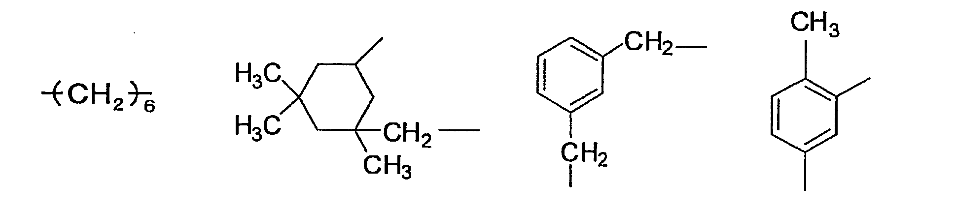


- The barrier film according to any one of Claims 1 to 8, wherein the polymerizable component of the organic layer further contains a monofunctional monomer.
- The barrier film according to any one of Claims 1 to 9, wherein the organic layer has a thickness of 50 to 5000 nm.
- The barrier film according to any one of Claims 1 to 10, wherein the inorganic layer has a thickness of 10 to 300 nm.
- An device comprising a barrier film according to any one of Claims 1 to 11.
- An organic EL device comprising a barrier film according to any one of Claims 1 to 11.
Applications Claiming Priority (1)
| Application Number | Priority Date | Filing Date | Title |
|---|---|---|---|
| JP2007128389 | 2007-05-14 |
Publications (3)
| Publication Number | Publication Date |
|---|---|
| EP2052855A2 true EP2052855A2 (en) | 2009-04-29 |
| EP2052855A3 EP2052855A3 (en) | 2009-05-06 |
| EP2052855B1 EP2052855B1 (en) | 2012-01-25 |
Family
ID=40123364
Family Applications (1)
| Application Number | Title | Priority Date | Filing Date |
|---|---|---|---|
| EP20080008940 Active EP2052855B1 (en) | 2007-05-14 | 2008-05-14 | Barrier film and device |
Country Status (5)
| Country | Link |
|---|---|
| US (1) | US8057904B2 (en) |
| EP (1) | EP2052855B1 (en) |
| JP (1) | JP5198131B2 (en) |
| CN (1) | CN101306589B (en) |
| AT (1) | ATE542843T1 (en) |
Cited By (1)
| Publication number | Priority date | Publication date | Assignee | Title |
|---|---|---|---|---|
| CN113646391A (en) * | 2019-04-08 | 2021-11-12 | 魁北克电力公司 | Protective material for lithium metal anodes, method for the production thereof and use thereof |
Families Citing this family (36)
| Publication number | Priority date | Publication date | Assignee | Title |
|---|---|---|---|---|
| JP5246839B2 (en) * | 2006-08-24 | 2013-07-24 | 独立行政法人産業技術総合研究所 | Semiconductor thin film manufacturing method, semiconductor thin film manufacturing apparatus, photoelectric conversion element manufacturing method, and photoelectric conversion element |
| JP5354733B2 (en) * | 2008-07-29 | 2013-11-27 | 日東電工株式会社 | Polarizer protective film and polarizing plate and image display device using polarizer protective film |
| JP5348986B2 (en) * | 2008-09-25 | 2013-11-20 | 富士フイルム株式会社 | Conductive material and manufacturing method thereof |
| JP2010165721A (en) * | 2009-01-13 | 2010-07-29 | Honda Motor Co Ltd | Solar cell module |
| JP2010171270A (en) * | 2009-01-23 | 2010-08-05 | Denka Agsp Kk | Substrate for mounting light-emitting element and method of manufacturing the same |
| DE102009010990A1 (en) * | 2009-02-19 | 2010-08-26 | Karl Wörwag Lack- Und Farbenfabrik Gmbh & Co. Kg | Solar cell module and method for its production |
| US8318530B2 (en) * | 2009-07-24 | 2012-11-27 | Solopower, Inc. | Solar cell buffer layer having varying composition |
| US9101005B2 (en) * | 2009-09-15 | 2015-08-04 | Industrial Technology Research Institute | Package of environmental sensitive element |
| JP2011201064A (en) * | 2010-03-24 | 2011-10-13 | Fujifilm Corp | Barrier laminate, method for manufacturing the same, gas barrier film and device |
| JP5334900B2 (en) * | 2010-03-25 | 2013-11-06 | 富士フイルム株式会社 | Gas barrier film and device |
| US20120097234A1 (en) * | 2010-10-26 | 2012-04-26 | International Business Machines Corporation | Using Diffusion Barrier Layer for CuZnSn(S,Se) Thin Film Solar Cell |
| US20120100663A1 (en) * | 2010-10-26 | 2012-04-26 | International Business Machines Corporation | Fabrication of CuZnSn(S,Se) Thin Film Solar Cell with Valve Controlled S and Se |
| US9612378B2 (en) * | 2010-12-31 | 2017-04-04 | Cheil Industries, Inc. | Folder type polarizing film for organic light emitting diode |
| TWI429526B (en) * | 2011-12-15 | 2014-03-11 | Ind Tech Res Inst | Low water-vapor permeable composite film and packaging structure |
| KR101801913B1 (en) * | 2012-03-23 | 2017-11-28 | 삼성디스플레이 주식회사 | Organic light emitting display device and the method for manufacturing the same |
| DE102012009691B4 (en) * | 2012-05-15 | 2021-12-09 | Carl Zeiss Vision International Gmbh | Anti-fog coating on an optical component, optical component with this anti-fog coating and a method for producing this anti-fog coating |
| JP2014058154A (en) * | 2012-08-23 | 2014-04-03 | Toppan Printing Co Ltd | Gas barrier film and protective sheet for solar battery module |
| CN103904232A (en) * | 2012-12-25 | 2014-07-02 | 海洋王照明科技股份有限公司 | Organic light-emitting device and preparation method |
| CN103904226A (en) * | 2012-12-25 | 2014-07-02 | 海洋王照明科技股份有限公司 | Organic light-emitting device and preparation method |
| CN103904230B (en) * | 2012-12-25 | 2016-04-27 | 海洋王照明科技股份有限公司 | A kind of organic electroluminescence device and preparation method thereof |
| CN103904231B (en) * | 2012-12-25 | 2016-03-30 | 海洋王照明科技股份有限公司 | A kind of organic electroluminescence device and preparation method thereof |
| CN103904245A (en) * | 2012-12-25 | 2014-07-02 | 海洋王照明科技股份有限公司 | Organic electroluminescent device and preparing method thereof |
| KR20140097940A (en) | 2013-01-30 | 2014-08-07 | 삼성디스플레이 주식회사 | TFT substrate including barrier layer including silicon oxide layer and silicon silicon nitride layer, Organic light-emitting device comprising the TFT substrate, and the manufacturing method of the TFT substrate |
| CN105229801B (en) | 2013-02-07 | 2017-03-15 | 第一太阳能有限公司 | Photovoltaic device with protective layer on window layer and manufacturing method thereof |
| CN104037353A (en) * | 2013-03-07 | 2014-09-10 | 海洋王照明科技股份有限公司 | Organic light emission diode and preparation method thereof |
| CN104051645A (en) * | 2013-03-15 | 2014-09-17 | 海洋王照明科技股份有限公司 | Organic electroluminescent device and packaging method thereof |
| KR20140148204A (en) * | 2013-06-21 | 2014-12-31 | 삼성디스플레이 주식회사 | Window for display device and display device including the window panel |
| EP3040442B1 (en) | 2013-08-30 | 2024-02-14 | IUCF-HYU (Industry-University Cooperation Foundation Hanyang University) | Functional thin films comprising an hybrid organic/inorganic thin films and method of manufacturing same |
| JP5977776B2 (en) * | 2014-03-12 | 2016-08-24 | 富士フイルム株式会社 | Barrier laminate, gas barrier film, laminate film, and infusion bag |
| JP6280477B2 (en) * | 2014-09-26 | 2018-02-14 | 富士フイルム株式会社 | Gas barrier film and method for producing gas barrier film |
| CN104943301B (en) * | 2015-06-23 | 2017-05-31 | 宁波长阳科技股份有限公司 | A kind of superelevation intercepts optical polyester film and preparation method thereof |
| JP6469605B2 (en) * | 2016-03-10 | 2019-02-13 | 富士フイルム株式会社 | Gas barrier film |
| CN111602467B (en) * | 2018-01-31 | 2023-08-29 | 日本瑞翁株式会社 | Resin film and organic electroluminescent device |
| KR102202929B1 (en) * | 2018-04-17 | 2021-01-14 | 주식회사 엘지화학 | Barrier film having light-dffusing property |
| US20200000082A1 (en) | 2018-06-28 | 2020-01-02 | Tony Gonzales | Scorpion repel surface treatments and method for same |
| JP7325981B2 (en) * | 2019-03-20 | 2023-08-15 | 日東電工株式会社 | Laminate, piezoelectric device using same, and method for manufacturing piezoelectric device |
Citations (3)
| Publication number | Priority date | Publication date | Assignee | Title |
|---|---|---|---|---|
| JP2003053881A (en) | 2001-08-10 | 2003-02-26 | Sumitomo Bakelite Co Ltd | Plastic film having water vapor barrier properties |
| JP2005279974A (en) | 2004-03-26 | 2005-10-13 | Mitsui Chemicals Inc | Transparent gas barrier film |
| JP2005313560A (en) | 2004-04-30 | 2005-11-10 | Dainippon Printing Co Ltd | Gas barrier film |
Family Cites Families (21)
| Publication number | Priority date | Publication date | Assignee | Title |
|---|---|---|---|---|
| CN1012611B (en) * | 1989-11-06 | 1991-05-15 | 黑龙江省绥棱县塑料二厂 | Resin composite non-woven fabric waterproof coiled material and production method thereof |
| JP3206824B2 (en) * | 1991-11-27 | 2001-09-10 | シーアイ化成株式会社 | Polyester film for decorative sheet |
| US6083628A (en) | 1994-11-04 | 2000-07-04 | Sigma Laboratories Of Arizona, Inc. | Hybrid polymer film |
| US6013363A (en) * | 1997-03-17 | 2000-01-11 | Oji-Yuka Synthetic Paper Co., Ltd. | Packaging material |
| US6074097A (en) * | 1997-04-28 | 2000-06-13 | Dai Nippon Printing Co., Ltd. | Package, package manufacturing method and package manufacturing system for carrying out the package manufacturing method |
| JPH11131045A (en) * | 1997-10-28 | 1999-05-18 | Nippon Polyurethane Ind Co Ltd | Laminating adhesive |
| JP2001079994A (en) * | 1999-09-10 | 2001-03-27 | Unitika Ltd | Easily adhesive plastic film and its manufacturing method |
| JP2002036454A (en) * | 2000-07-31 | 2002-02-05 | Sumitomo Chem Co Ltd | Laminates and containers |
| CN2477727Y (en) * | 2001-05-30 | 2002-02-20 | 张家华 | Separating membrane composite |
| JP2003053902A (en) * | 2001-08-22 | 2003-02-26 | Toppan Printing Co Ltd | Packaging material |
| JP2003191370A (en) * | 2001-12-26 | 2003-07-08 | Sumitomo Bakelite Co Ltd | Water vapor barrier plastic film and display substrate for electroluminescence using the same |
| JP4028259B2 (en) * | 2002-03-06 | 2007-12-26 | 大日本印刷株式会社 | Gas barrier vapor deposition laminate |
| JP2003251733A (en) * | 2002-03-07 | 2003-09-09 | Nitto Denko Corp | Transparent gas barrier film, and transparent conductive electrode substrate, display element, solar cell or planar light-emitting body using the same |
| US6866949B2 (en) * | 2002-03-08 | 2005-03-15 | Dai Nippon Printing Co., Ltd. | Substrate film, gas barrier film, and display using the same |
| ITTO20020362A1 (en) | 2002-04-30 | 2003-10-30 | Metlac S P A | MULTI-COVERING SYSTEM WITH GAS BARRIER PROPERTIES, PHOTORETICULABLE BY UV RADIATION PARTICULARLY SUITABLE FOR PROTECTION |
| EP1561765A4 (en) * | 2002-11-08 | 2007-07-04 | Mitsubishi Chem Corp | RADIATION-CURABLE RESIN COMPOSITION AND CURED PRODUCT |
| JP2005054145A (en) * | 2003-08-07 | 2005-03-03 | Mitsubishi Gas Chem Co Inc | Gas barrier (meth) acrylate resin cured product and paint, adhesive, film |
| CN1810502A (en) * | 2005-01-28 | 2006-08-02 | 朱家牧 | Low temperature high shrinkage and high obstruction membrane and its production process |
| US7326448B2 (en) | 2005-02-17 | 2008-02-05 | 3M Innovative Properties Company | Polymerizable oligomeric urethane compositions comprising nanoparticles |
| JP2006253055A (en) * | 2005-03-14 | 2006-09-21 | Toppan Printing Co Ltd | Flexible substrate for organic electroluminescence device and organic electroluminescence device using the same |
| JP4716773B2 (en) | 2005-04-06 | 2011-07-06 | 富士フイルム株式会社 | Gas barrier film and organic device using the same |
-
2008
- 2008-04-21 JP JP2008110476A patent/JP5198131B2/en not_active Expired - Fee Related
- 2008-05-12 US US12/119,129 patent/US8057904B2/en not_active Expired - Fee Related
- 2008-05-14 CN CN2008100970939A patent/CN101306589B/en not_active Expired - Fee Related
- 2008-05-14 EP EP20080008940 patent/EP2052855B1/en active Active
- 2008-05-14 AT AT08008940T patent/ATE542843T1/en active
Patent Citations (3)
| Publication number | Priority date | Publication date | Assignee | Title |
|---|---|---|---|---|
| JP2003053881A (en) | 2001-08-10 | 2003-02-26 | Sumitomo Bakelite Co Ltd | Plastic film having water vapor barrier properties |
| JP2005279974A (en) | 2004-03-26 | 2005-10-13 | Mitsui Chemicals Inc | Transparent gas barrier film |
| JP2005313560A (en) | 2004-04-30 | 2005-11-10 | Dainippon Printing Co Ltd | Gas barrier film |
Cited By (2)
| Publication number | Priority date | Publication date | Assignee | Title |
|---|---|---|---|---|
| CN113646391A (en) * | 2019-04-08 | 2021-11-12 | 魁北克电力公司 | Protective material for lithium metal anodes, method for the production thereof and use thereof |
| CN113646391B (en) * | 2019-04-08 | 2024-03-05 | 魁北克电力公司 | Protective materials for lithium metal anodes, preparation methods and uses thereof |
Also Published As
| Publication number | Publication date |
|---|---|
| JP5198131B2 (en) | 2013-05-15 |
| US20080318034A1 (en) | 2008-12-25 |
| CN101306589B (en) | 2012-08-22 |
| EP2052855B1 (en) | 2012-01-25 |
| CN101306589A (en) | 2008-11-19 |
| JP2008307887A (en) | 2008-12-25 |
| EP2052855A3 (en) | 2009-05-06 |
| US8057904B2 (en) | 2011-11-15 |
| ATE542843T1 (en) | 2012-02-15 |
Similar Documents
| Publication | Publication Date | Title |
|---|---|---|
| EP2052855B1 (en) | Barrier film and device | |
| EP1842873B1 (en) | Gas-barrier laminate film | |
| EP2033988B1 (en) | Gas-barrier film, and method for sealing display device with gas-barrier film | |
| EP2045355A1 (en) | Gas-barrier film and organic device comprising same | |
| EP2172988A2 (en) | Organic solar cell device | |
| CN101391498A (en) | Gas barrier thin film and organic device using the same | |
| EP2040314A1 (en) | Light-emitting device or display device, and method for producing them | |
| US10665738B2 (en) | Gas barrier film, solar cell, and manufacturing method of gas barrier film | |
| EP2056372A2 (en) | Gas barrier film and organic device using the same | |
| KR20090028450A (en) | Gas barrier film and display element using the same | |
| WO2011158874A1 (en) | Organic thin film solar cell | |
| EP2036717B1 (en) | Gas barrier film, and display device comprising the same | |
| EP3337848B1 (en) | Composite article including a multilayer barrier assembly and methods of making the same | |
| EP3337847B1 (en) | Composite article and methods of making the same | |
| US11752749B2 (en) | Composite article including a multilayer barrier assembly and methods of making the same | |
| JP2018138381A (en) | Laminate |
Legal Events
| Date | Code | Title | Description |
|---|---|---|---|
| PUAI | Public reference made under article 153(3) epc to a published international application that has entered the european phase |
Free format text: ORIGINAL CODE: 0009012 |
|
| PUAL | Search report despatched |
Free format text: ORIGINAL CODE: 0009013 |
|
| AK | Designated contracting states |
Kind code of ref document: A2 Designated state(s): AT BE BG CH CY CZ DE DK EE ES FI FR GB GR HR HU IE IS IT LI LT LU LV MC MT NL NO PL PT RO SE SI SK TR |
|
| AX | Request for extension of the european patent |
Extension state: AL BA MK RS |
|
| AK | Designated contracting states |
Kind code of ref document: A3 Designated state(s): AT BE BG CH CY CZ DE DK EE ES FI FR GB GR HR HU IE IS IT LI LT LU LV MC MT NL NO PL PT RO SE SI SK TR |
|
| AX | Request for extension of the european patent |
Extension state: AL BA MK RS |
|
| RIC1 | Information provided on ipc code assigned before grant |
Ipc: C08G 18/67 20060101AFI20090330BHEP Ipc: C09D 175/16 20060101ALI20090330BHEP Ipc: H01L 51/52 20060101ALI20090330BHEP |
|
| RIN1 | Information on inventor provided before grant (corrected) |
Inventor name: KOBAYASHI, TAKASHI C/O FUJIFILM CORPORATION Inventor name: MURAKAMI, TOMOO C/O FUJIFILM CORPORATION |
|
| 17P | Request for examination filed |
Effective date: 20091106 |
|
| AKX | Designation fees paid |
Designated state(s): AT BE BG CH CY CZ DE DK EE ES FI FR GB GR HR HU IE IS IT LI LT LU LV MC MT NL NO PL PT RO SE SI SK TR |
|
| AXX | Extension fees paid |
Extension state: MK Payment date: 20091106 Extension state: BA Payment date: 20091106 Extension state: RS Payment date: 20091106 Extension state: AL Payment date: 20091106 |
|
| GRAP | Despatch of communication of intention to grant a patent |
Free format text: ORIGINAL CODE: EPIDOSNIGR1 |
|
| GRAS | Grant fee paid |
Free format text: ORIGINAL CODE: EPIDOSNIGR3 |
|
| GRAA | (expected) grant |
Free format text: ORIGINAL CODE: 0009210 |
|
| RIN1 | Information on inventor provided before grant (corrected) |
Inventor name: KOBAYASHI, TAKASHI C/O FUJIFILM CORPORATION Inventor name: MURAKAMI, TOMOO C/O FUJIFILM CORPORATION |
|
| AK | Designated contracting states |
Kind code of ref document: B1 Designated state(s): AT BE BG CH CY CZ DE DK EE ES FI FR GB GR HR HU IE IS IT LI LT LU LV MC MT NL NO PL PT RO SE SI SK TR |
|
| AX | Request for extension of the european patent |
Extension state: AL BA MK RS |
|
| REG | Reference to a national code |
Ref country code: GB Ref legal event code: FG4D |
|
| REG | Reference to a national code |
Ref country code: CH Ref legal event code: EP |
|
| REG | Reference to a national code |
Ref country code: AT Ref legal event code: REF Ref document number: 542843 Country of ref document: AT Kind code of ref document: T Effective date: 20120215 |
|
| REG | Reference to a national code |
Ref country code: IE Ref legal event code: FG4D |
|
| REG | Reference to a national code |
Ref country code: DE Ref legal event code: R096 Ref document number: 602008012803 Country of ref document: DE Effective date: 20120329 |
|
| REG | Reference to a national code |
Ref country code: NL Ref legal event code: VDEP Effective date: 20120125 |
|
| LTIE | Lt: invalidation of european patent or patent extension |
Effective date: 20120125 |
|
| PG25 | Lapsed in a contracting state [announced via postgrant information from national office to epo] |
Ref country code: LT Free format text: LAPSE BECAUSE OF FAILURE TO SUBMIT A TRANSLATION OF THE DESCRIPTION OR TO PAY THE FEE WITHIN THE PRESCRIBED TIME-LIMIT Effective date: 20120125 Ref country code: BG Free format text: LAPSE BECAUSE OF FAILURE TO SUBMIT A TRANSLATION OF THE DESCRIPTION OR TO PAY THE FEE WITHIN THE PRESCRIBED TIME-LIMIT Effective date: 20120425 Ref country code: IS Free format text: LAPSE BECAUSE OF FAILURE TO SUBMIT A TRANSLATION OF THE DESCRIPTION OR TO PAY THE FEE WITHIN THE PRESCRIBED TIME-LIMIT Effective date: 20120525 Ref country code: HR Free format text: LAPSE BECAUSE OF FAILURE TO SUBMIT A TRANSLATION OF THE DESCRIPTION OR TO PAY THE FEE WITHIN THE PRESCRIBED TIME-LIMIT Effective date: 20120125 Ref country code: NL Free format text: LAPSE BECAUSE OF FAILURE TO SUBMIT A TRANSLATION OF THE DESCRIPTION OR TO PAY THE FEE WITHIN THE PRESCRIBED TIME-LIMIT Effective date: 20120125 Ref country code: BE Free format text: LAPSE BECAUSE OF FAILURE TO SUBMIT A TRANSLATION OF THE DESCRIPTION OR TO PAY THE FEE WITHIN THE PRESCRIBED TIME-LIMIT Effective date: 20120125 Ref country code: NO Free format text: LAPSE BECAUSE OF FAILURE TO SUBMIT A TRANSLATION OF THE DESCRIPTION OR TO PAY THE FEE WITHIN THE PRESCRIBED TIME-LIMIT Effective date: 20120425 |
|
| PGFP | Annual fee paid to national office [announced via postgrant information from national office to epo] |
Ref country code: DE Payment date: 20120516 Year of fee payment: 5 |
|
| PG25 | Lapsed in a contracting state [announced via postgrant information from national office to epo] |
Ref country code: FI Free format text: LAPSE BECAUSE OF FAILURE TO SUBMIT A TRANSLATION OF THE DESCRIPTION OR TO PAY THE FEE WITHIN THE PRESCRIBED TIME-LIMIT Effective date: 20120125 Ref country code: GR Free format text: LAPSE BECAUSE OF FAILURE TO SUBMIT A TRANSLATION OF THE DESCRIPTION OR TO PAY THE FEE WITHIN THE PRESCRIBED TIME-LIMIT Effective date: 20120426 Ref country code: PL Free format text: LAPSE BECAUSE OF FAILURE TO SUBMIT A TRANSLATION OF THE DESCRIPTION OR TO PAY THE FEE WITHIN THE PRESCRIBED TIME-LIMIT Effective date: 20120125 Ref country code: PT Free format text: LAPSE BECAUSE OF FAILURE TO SUBMIT A TRANSLATION OF THE DESCRIPTION OR TO PAY THE FEE WITHIN THE PRESCRIBED TIME-LIMIT Effective date: 20120525 Ref country code: LV Free format text: LAPSE BECAUSE OF FAILURE TO SUBMIT A TRANSLATION OF THE DESCRIPTION OR TO PAY THE FEE WITHIN THE PRESCRIBED TIME-LIMIT Effective date: 20120125 |
|
| REG | Reference to a national code |
Ref country code: AT Ref legal event code: MK05 Ref document number: 542843 Country of ref document: AT Kind code of ref document: T Effective date: 20120125 |
|
| PG25 | Lapsed in a contracting state [announced via postgrant information from national office to epo] |
Ref country code: CY Free format text: LAPSE BECAUSE OF FAILURE TO SUBMIT A TRANSLATION OF THE DESCRIPTION OR TO PAY THE FEE WITHIN THE PRESCRIBED TIME-LIMIT Effective date: 20120125 |
|
| PG25 | Lapsed in a contracting state [announced via postgrant information from national office to epo] |
Ref country code: RO Free format text: LAPSE BECAUSE OF FAILURE TO SUBMIT A TRANSLATION OF THE DESCRIPTION OR TO PAY THE FEE WITHIN THE PRESCRIBED TIME-LIMIT Effective date: 20120125 Ref country code: EE Free format text: LAPSE BECAUSE OF FAILURE TO SUBMIT A TRANSLATION OF THE DESCRIPTION OR TO PAY THE FEE WITHIN THE PRESCRIBED TIME-LIMIT Effective date: 20120125 Ref country code: DK Free format text: LAPSE BECAUSE OF FAILURE TO SUBMIT A TRANSLATION OF THE DESCRIPTION OR TO PAY THE FEE WITHIN THE PRESCRIBED TIME-LIMIT Effective date: 20120125 Ref country code: SI Free format text: LAPSE BECAUSE OF FAILURE TO SUBMIT A TRANSLATION OF THE DESCRIPTION OR TO PAY THE FEE WITHIN THE PRESCRIBED TIME-LIMIT Effective date: 20120125 Ref country code: CZ Free format text: LAPSE BECAUSE OF FAILURE TO SUBMIT A TRANSLATION OF THE DESCRIPTION OR TO PAY THE FEE WITHIN THE PRESCRIBED TIME-LIMIT Effective date: 20120125 Ref country code: SE Free format text: LAPSE BECAUSE OF FAILURE TO SUBMIT A TRANSLATION OF THE DESCRIPTION OR TO PAY THE FEE WITHIN THE PRESCRIBED TIME-LIMIT Effective date: 20120125 |
|
| PG25 | Lapsed in a contracting state [announced via postgrant information from national office to epo] |
Ref country code: SK Free format text: LAPSE BECAUSE OF FAILURE TO SUBMIT A TRANSLATION OF THE DESCRIPTION OR TO PAY THE FEE WITHIN THE PRESCRIBED TIME-LIMIT Effective date: 20120125 Ref country code: IT Free format text: LAPSE BECAUSE OF FAILURE TO SUBMIT A TRANSLATION OF THE DESCRIPTION OR TO PAY THE FEE WITHIN THE PRESCRIBED TIME-LIMIT Effective date: 20120125 |
|
| PLBE | No opposition filed within time limit |
Free format text: ORIGINAL CODE: 0009261 |
|
| STAA | Information on the status of an ep patent application or granted ep patent |
Free format text: STATUS: NO OPPOSITION FILED WITHIN TIME LIMIT |
|
| PG25 | Lapsed in a contracting state [announced via postgrant information from national office to epo] |
Ref country code: MC Free format text: LAPSE BECAUSE OF NON-PAYMENT OF DUE FEES Effective date: 20120531 |
|
| REG | Reference to a national code |
Ref country code: CH Ref legal event code: PL |
|
| 26N | No opposition filed |
Effective date: 20121026 |
|
| GBPC | Gb: european patent ceased through non-payment of renewal fee |
Effective date: 20120514 |
|
| PG25 | Lapsed in a contracting state [announced via postgrant information from national office to epo] |
Ref country code: LI Free format text: LAPSE BECAUSE OF NON-PAYMENT OF DUE FEES Effective date: 20120531 Ref country code: AT Free format text: LAPSE BECAUSE OF FAILURE TO SUBMIT A TRANSLATION OF THE DESCRIPTION OR TO PAY THE FEE WITHIN THE PRESCRIBED TIME-LIMIT Effective date: 20120125 Ref country code: CH Free format text: LAPSE BECAUSE OF NON-PAYMENT OF DUE FEES Effective date: 20120531 |
|
| REG | Reference to a national code |
Ref country code: DE Ref legal event code: R097 Ref document number: 602008012803 Country of ref document: DE Effective date: 20121026 |
|
| REG | Reference to a national code |
Ref country code: IE Ref legal event code: MM4A |
|
| REG | Reference to a national code |
Ref country code: FR Ref legal event code: ST Effective date: 20130131 |
|
| PG25 | Lapsed in a contracting state [announced via postgrant information from national office to epo] |
Ref country code: GB Free format text: LAPSE BECAUSE OF NON-PAYMENT OF DUE FEES Effective date: 20120514 Ref country code: ES Free format text: LAPSE BECAUSE OF FAILURE TO SUBMIT A TRANSLATION OF THE DESCRIPTION OR TO PAY THE FEE WITHIN THE PRESCRIBED TIME-LIMIT Effective date: 20120506 Ref country code: IE Free format text: LAPSE BECAUSE OF NON-PAYMENT OF DUE FEES Effective date: 20120514 Ref country code: FR Free format text: LAPSE BECAUSE OF NON-PAYMENT OF DUE FEES Effective date: 20120531 |
|
| PG25 | Lapsed in a contracting state [announced via postgrant information from national office to epo] |
Ref country code: MT Free format text: LAPSE BECAUSE OF FAILURE TO SUBMIT A TRANSLATION OF THE DESCRIPTION OR TO PAY THE FEE WITHIN THE PRESCRIBED TIME-LIMIT Effective date: 20120125 |
|
| PG25 | Lapsed in a contracting state [announced via postgrant information from national office to epo] |
Ref country code: DE Free format text: LAPSE BECAUSE OF NON-PAYMENT OF DUE FEES Effective date: 20131203 |
|
| REG | Reference to a national code |
Ref country code: DE Ref legal event code: R119 Ref document number: 602008012803 Country of ref document: DE Effective date: 20131203 |
|
| PG25 | Lapsed in a contracting state [announced via postgrant information from national office to epo] |
Ref country code: TR Free format text: LAPSE BECAUSE OF FAILURE TO SUBMIT A TRANSLATION OF THE DESCRIPTION OR TO PAY THE FEE WITHIN THE PRESCRIBED TIME-LIMIT Effective date: 20120125 |
|
| PG25 | Lapsed in a contracting state [announced via postgrant information from national office to epo] |
Ref country code: LU Free format text: LAPSE BECAUSE OF NON-PAYMENT OF DUE FEES Effective date: 20120514 |
|
| PG25 | Lapsed in a contracting state [announced via postgrant information from national office to epo] |
Ref country code: HU Free format text: LAPSE BECAUSE OF FAILURE TO SUBMIT A TRANSLATION OF THE DESCRIPTION OR TO PAY THE FEE WITHIN THE PRESCRIBED TIME-LIMIT Effective date: 20080514 |