EP2051501A2 - Photo sensor with a low-noise photo element, sub-linear response and global shutter field of the invention - Google Patents
Photo sensor with a low-noise photo element, sub-linear response and global shutter field of the invention Download PDFInfo
- Publication number
- EP2051501A2 EP2051501A2 EP08166226A EP08166226A EP2051501A2 EP 2051501 A2 EP2051501 A2 EP 2051501A2 EP 08166226 A EP08166226 A EP 08166226A EP 08166226 A EP08166226 A EP 08166226A EP 2051501 A2 EP2051501 A2 EP 2051501A2
- Authority
- EP
- European Patent Office
- Prior art keywords
- voltage
- photo sensor
- sub
- linear
- transistor
- Prior art date
- Legal status (The legal status is an assumption and is not a legal conclusion. Google has not performed a legal analysis and makes no representation as to the accuracy of the status listed.)
- Withdrawn
Links
Images


Classifications
-
- H—ELECTRICITY
- H04—ELECTRIC COMMUNICATION TECHNIQUE
- H04N—PICTORIAL COMMUNICATION, e.g. TELEVISION
- H04N25/00—Circuitry of solid-state image sensors [SSIS]; Control thereof
- H04N25/50—Control of the SSIS exposure
- H04N25/57—Control of the dynamic range
-
- H—ELECTRICITY
- H04—ELECTRIC COMMUNICATION TECHNIQUE
- H04N—PICTORIAL COMMUNICATION, e.g. TELEVISION
- H04N25/00—Circuitry of solid-state image sensors [SSIS]; Control thereof
- H04N25/50—Control of the SSIS exposure
- H04N25/53—Control of the integration time
- H04N25/532—Control of the integration time by controlling global shutters in CMOS SSIS
-
- H—ELECTRICITY
- H04—ELECTRIC COMMUNICATION TECHNIQUE
- H04N—PICTORIAL COMMUNICATION, e.g. TELEVISION
- H04N25/00—Circuitry of solid-state image sensors [SSIS]; Control thereof
- H04N25/60—Noise processing, e.g. detecting, correcting, reducing or removing noise
- H04N25/616—Noise processing, e.g. detecting, correcting, reducing or removing noise involving a correlated sampling function, e.g. correlated double sampling [CDS] or triple sampling
-
- H—ELECTRICITY
- H04—ELECTRIC COMMUNICATION TECHNIQUE
- H04N—PICTORIAL COMMUNICATION, e.g. TELEVISION
- H04N25/00—Circuitry of solid-state image sensors [SSIS]; Control thereof
- H04N25/60—Noise processing, e.g. detecting, correcting, reducing or removing noise
- H04N25/63—Noise processing, e.g. detecting, correcting, reducing or removing noise applied to dark current
-
- H—ELECTRICITY
- H04—ELECTRIC COMMUNICATION TECHNIQUE
- H04N—PICTORIAL COMMUNICATION, e.g. TELEVISION
- H04N25/00—Circuitry of solid-state image sensors [SSIS]; Control thereof
- H04N25/70—SSIS architectures; Circuits associated therewith
- H04N25/76—Addressed sensors, e.g. MOS or CMOS sensors
- H04N25/77—Pixel circuitry, e.g. memories, A/D converters, pixel amplifiers, shared circuits or shared components
-
- H—ELECTRICITY
- H04—ELECTRIC COMMUNICATION TECHNIQUE
- H04N—PICTORIAL COMMUNICATION, e.g. TELEVISION
- H04N25/00—Circuitry of solid-state image sensors [SSIS]; Control thereof
- H04N25/70—SSIS architectures; Circuits associated therewith
- H04N25/76—Addressed sensors, e.g. MOS or CMOS sensors
- H04N25/77—Pixel circuitry, e.g. memories, A/D converters, pixel amplifiers, shared circuits or shared components
- H04N25/771—Pixel circuitry, e.g. memories, A/D converters, pixel amplifiers, shared circuits or shared components comprising storage means other than floating diffusion
Definitions
- the present invention relates to imaging devices and more specifically, to imaging devices that are based on solid-state photo sensors.
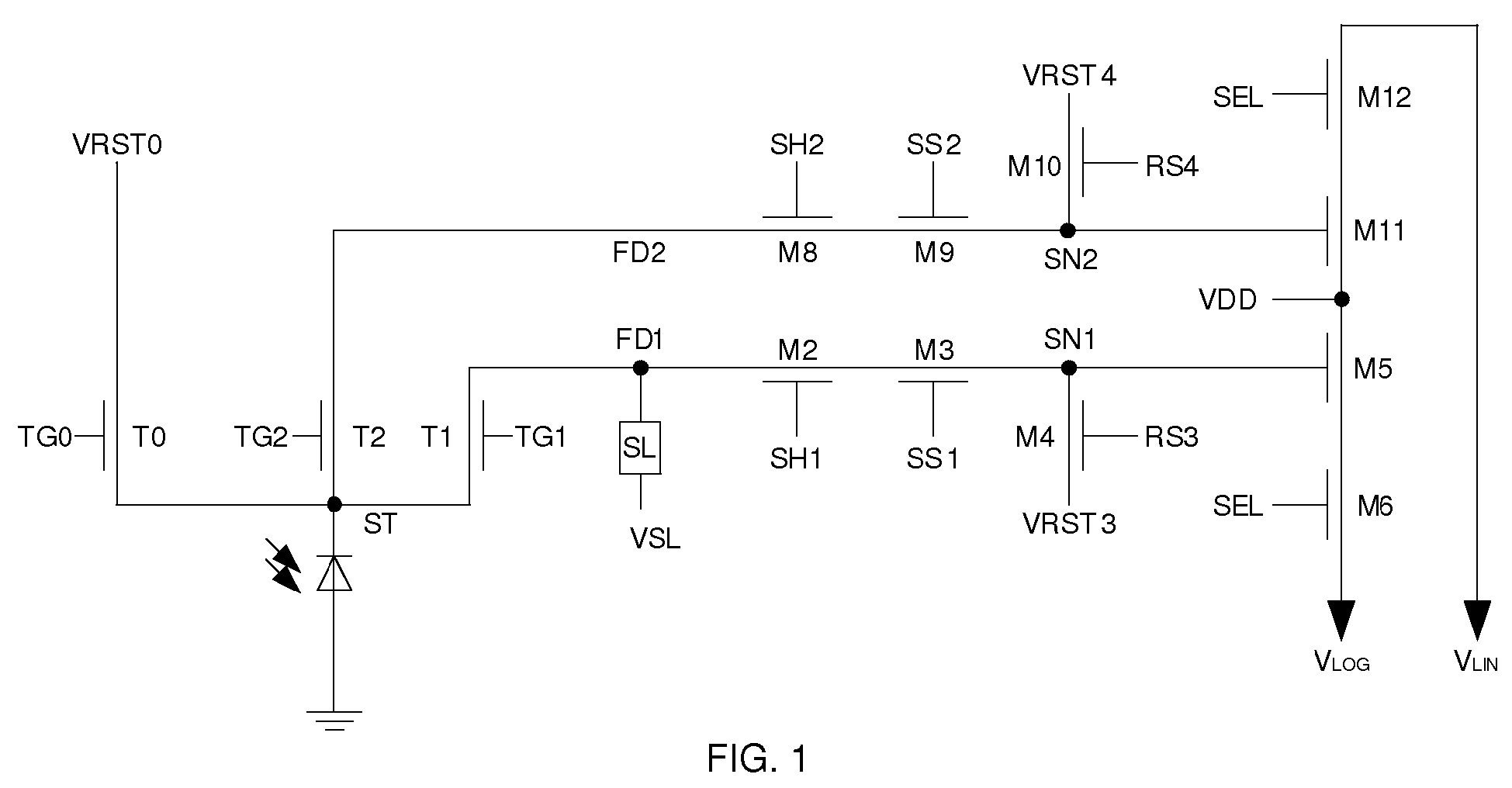
- FIG. 1 schematically shows a pixel that allows global shutter and integrate-while-read, using two output channels for maximum speed, according to an embodiment of the invention
- FIG. 2 schematically depicts 3 different possibilities of combining the reset transistor and the sub-linear element, according to some embodiments of the invention
- FIG. 3 schematically shows the pixel from FIG. 1 without a global reset at the PPD node
- FIG. 4 schematically illustrates a modification of the pixel in FIG. 3 , where only one output path is used
- FIG. 5 schematically shows the pixel from FIG. 4 without a sampling transistor in the sub-linear path
- FIG. 6 shows a pixel without shutter transistors, but two output paths for high speed read-out
- FIG. 7 schematically shows a basic pixel with sub-linear element and a shutter transistor.
- Fig. 8 shows a voltage diagram for large illumination levels.
- Embodiments of the present invention enable for example the implementation of low-noise, low-smear, low-dark-current, one-dimensional and two-dimensional image sensing, where it is necessary to increase the dynamic range while having a global shutter functionality at the same time.
- the invention relates in embodiments to a photo sensor for generating photoinduced charge carriers, wherein the photo sensor is implemented by one of the following: a pinned photo diode (PPD), a buried photo diode, and a charge-coupled device (CCD).
- PPD pinned photo diode
- CCD charge-coupled device
- the photo sensor comprises at least one transfer gate to release the charge into at least one respective floating diffusion node, a sub-linear element connected to the at least one floating diffusion node, a sub-linear voltage source for which the voltage drop depends in a sub-linear fashion on a current through photo sensor, and a first transistor connected between the floating diffusion and a sense node, and a second transistor between the sense node and the reset voltage, a third transistor, a fourth transistor, a source follower and a select transistor for measuring a measured voltage indicative of a voltage at the floating diffusion node, a control circuitry adapted to run at least one measuring cycle.
- each measuring cycle comprises the following three phases: a) in a first phase the control circuit issues a first reset command to the second transistor and toggles a shutter signal high, and transfer gate between a spill-over voltage and a charge transfer voltage to completely empty the pinned photodiode storage node of the PPD; b) in a second phase a select signal of a pixel is controlled to measure a pixel's first reset voltage, then puts the shutter signal high to measure the pixel's sub-linear signal voltage, and issues a second reset command based on the measurement, and c) in a third phase the control circuit controls the pixel select signal to measure the pixel's second reset voltage, then puts the shutter signal high and operates the transfer gate to generate the pixel's fourth linear signal voltage.
- the first transistor M1 is a shutter transistor.
- the photo sensor further comprises a first sub-linear reset element connected between first floating diffusion node, the sub-linear voltage source and the first reset voltage, for which a voltage drop depend in a sub-linear fashion on a current through the photo sensor, and a second sub-linear reset element connected between a second floating diffusion node, a VSS and a second reset voltage.
- the second sub-linear reset element is a reset transistor.
- the photo sensor further comprises a fifth transistor, wherein the second and third transistor measures a first voltage on the first floating diffusion node, and the fourth and the fifth transistor measure a second voltage on the second floating diffusion node.
- the photo sensor further comprises a sixth, seventh and eighth transistor, wherein both the seventh and eighth transistor are operatively coupled between the second floating diffusion node and the sense node, wherein the second transistor is operatively coupled with the first floating diffusion node and the sense node, wherein the fourth transistor is operatively coupled with the reset voltage and the sense node, thus enabling the source follower and the select transistor to measure a measured the voltage at the sense node.
- the photo sensor further comprises a ninth transistor between the second floating diffusion node, a tenth transistor, an eleventh transistor, an twelfth transistor, a first sense node, a second sense node, wherein the third transistor is operatively coupled between the first floating diffusion node and the first sense node, wherein the eighth and the ninth transistor are between the second floating diffusion node and the second sense node, wherein the fourth transistor is operatively coupled between the first sense node and a third reset voltage, wherein the tenth transistor is operatively coupled between the second sense node and a fourth reset voltage respectively, wherein the fifth and sixth transistors measure a voltage indicative of a voltage at the first sense node, and wherein an eleventh and twelfth transistor measure a voltage at the second sense node.
- the photo sensor comprises a third transfer gate between a pinned photodiode storage node and fifth reset voltage.
- the sub-linear element is either one of the following: a diode and a diode connected transistor.
- the sub-linear reset element comprises either one of the following:
- the photo sensor may be implemented in CMOS-CCD hybrid image sensors whose photosensitive devices employ charge-coupled devices (CCD),
- CCD charge-coupled devices
- a photo sensor offering the advantages of a PPD or CCD combined with a sub-linear device, but also a global shutter functionality and means to enable high speed operation.
- a further object of the invention is to provide methods allowing integrate-while-read, a feature that is very often used in high speed imaging.
- the sensor comprises two transfer gates (T1 and T2) connecting the photo active element to two nodes FD1 and FD2, as is schematically illustrated in FIG. 1 .
- At least FD1 comprises a sub-linear element. Both nodes have independent reset transistors associated.
- FD1 is connected to node SN1 via two transistors (M2 and M3) in series.
- SN1 has another reset transistor M4 and a read-out structure (M5 and M6) connected.
- M6 connects to an output VLOG. From node FD2 a second signal path leads to an output VLIN.
- the parallel structure from the photo-active element to outputs VLIN and VLOG enables high speed operation.
- the reset transistors on the nodes FD1, FD2, SN1 and SN2 allow integrate-while-read.
- the series connection of M2 and M3 allows storing the signal from the sensor without immediate read-out. The same holds true for M8 and M9.
- Many photo sensors working in parallel can therefore be read-out sequentially and at the same time integrate the next signal on the photo-active element.
- the device can be operated in the following phases which may be part of repetitive measurement cycles:
- the photo sensor has the potential to offer, at the same time, low noise, low image lag and smear, low dark current, a high dynamic range, a global shutter and high speed operation capabilities.
- MOS transistors are of type NMOS.
- the invention however is not limit to the use of NMOS transistors.
- PMOS transistors or any combination of both types can be used to implement the pixels.
- the basic operation mode is illustrated with the pixel with reference to FIG. 7 and FIG. 8 .
- the exposure cycle is started by reverse biasing the PPD to its pinning potential and by setting the transfer gate (TG) to a non-zero skimming potential (VSP).
- Photo-generated charge carriers start to fill the PPD; if illumination intensity is high, excessive photo charges are flowing over the transfer gate (T1) to the floating diffusion node (FD).
- the sub-linear element generates a voltage on FD that is a sub-linear function of the illumination, hence increasing the dynamic range.
- the voltage at the sense node (SN) is read 4 times, namely at the end of the exposure time, after M1 transferred the sub-linear voltage level from FD to SN, after reset and after the photo charge in the buried channel has been transferred via FD to SN. This allows correlated multiple sampling techniques for eliminating reset noise.
- Reset of pixel FD and SN are reset to VRST if SH and RS are both high. By pulling TG high as well, also the PPD is reset: the storage node is empty and settles at VPIN.
- Exposure as soon as RS, SH and TG go low, integration of photo generated charges starts: the potential on ST drops as more and more charges are accumulated up to the level VSP. Now charges spill-over into FD. This current generates a voltage drop over the sub-linear element.
- the sub-linear part is read-out by activating SEL.
- the reset value VPRS1 is available at the output of the pixel.
- SH is put high to transfer the sub-linear part of the signal (if any) from FD to SN and further to the output of the pixel.
- the column amplifier samples VPSL.
- Read-out of linear part RS is again toggled low-high-low and SH is put low.
- the second reset value VPRS2 can be stored in the column amplifier. Afterwards SH and TG go high to transfer the linear part from the PPD to FD, SN and the output of the pixel.
- the column amplifier can calculate the difference between VPRS2 and VPLI. This scheme allows correlated double sampling of the linear part.
- FIG. 8 shows the case of large illumination levels, where the sub-linear element is activated by the charges spilling over T1. Consequently the linear part of the signal is equal to the full-well level of the PPD and does not have to be further processed.
- FIG. 6 implements the pixel from FIG. 7 using two read-out paths for high speed operation.
- SH is not necessary since VPRS1 and VPRS2 are stored on different nodes.
- the reset transistor and the sub-linear element are contained in the block labeled SL/RST1 and SL/RST2 and can be implemented using any of the three possibilities drawn in FIG. 2 : the right most version uses the reset transistor also as the sub-linear element by controlling the voltage at RS accordingly.
- FD1 holds the sub-linear part of the signal and FD2 the linear part. If two SL/RST blocks are used for symmetry, the SL element of SL/RST2 can be connected to the VSS.
- FIG. 5 shows a pixel that keeps FD1 and FD2 separately but uses one output path. Furthermore SH1, SH2 and SS are added to implement a global shutter functionality.
- the column amplifier has to support two modes: VPSL-VPRS1 and VPRS1-VLIN because the order at which the pixel values are output is different for the sub-linear and the linear part.
- the pixel in FIG. 4 is identical to the one of FIG. 5 except for the fact that sampling switches are used in both paths: this allows the same processing sequence in the column amplifier, that is to say a difference between a reset voltage and a signal level.
- FIG. 1 shows a high speed, high dynamic range, low noise pixel that allows integrate-while-read operation. The sequence of operation is detailed below:
- Exposure accumulation of charges starts as soon as TG0 is de-activated and stops when SH1 and TG2 were activated.
- Read-out the sub-linear value is sampled using SH1.
- the linear value is sampled by putting TG2 high and toggling SH2 as soon as SH1 is deactivated. Now both values are stored and TG0 can be activating to restart the next exposure immediately.
- SEL is now activated and two reset values can be sampled by the column amplifiers.
- SS1 and SS2 transfer the pixel values to SN1 and SN2 respectively where they are buffered into the column bus. As soon as the column amplifiers stored the difference to the preceding reset value the pixel is ready to be reset.
- Line reset SEL is put low, RS3, RS4, SSx and SHx are going high to reset FDx and SNx as well as the intermediate nodes of the pixel.
- the next line of pixels in the array can be processed.
Landscapes
- Engineering & Computer Science (AREA)
- Multimedia (AREA)
- Signal Processing (AREA)
- Transforming Light Signals Into Electric Signals (AREA)
- Solid State Image Pick-Up Elements (AREA)
Abstract
Description
- The present invention relates to imaging devices and more specifically, to imaging devices that are based on solid-state photo sensors.
-
- VSS = ground voltage
- PPD = pinned photodiode
- CCD = charge-coupled device
- ST = pinned photodiode storage node
- TG = transfer gate
- VRST = reset voltage
- VPIN = pinned photodiode potential
- VTX = charge transfer voltage on TG
- VSP = spill-over voltage on TG
- VSL = sub-linear element voltage
- VPRS1 =
pixel reset voltage 1 - VPSL = pixel's sub-linear signal voltage
- VPRS2 =
pixel reset voltage 2 - VPLI = pixel's linear signal voltage
- FD = floating diffusion
- RS = reset signal for FD or SN
- SH = shutter signal
- SS = sampling signal
- SN = sense node
- SEL = pixel select signal
- Conventional photodiodes as employed in complimentary metal-oxide semiconductor (CMOS) image sensors suffer from a set of practical limitations such as elevated dark current densities that can be overcome by the use of a pinned (or buried) photodiode (PPD). Unfortunately, the advantage of the PPD regarding low dark current is obtained at the expense of a limited dynamic range of typically less than 80dB. In conventional photodiode pixels, these limitations of the dynamic range can be overcome with the use of a sub-linear device connected the cathode of the photodiode, as taught for example in
US patent No. 6,815,685 (M.Wäny et al., "Photodetector and method for detecting radiation"). However this solution cannot be adopted for PPDs and charge-coupled devices (CCDs) because the storage node (ST) is internal to the device. By setting the voltage of the transfer gate (TG) to a well defined voltage to allow flowing excess charge into the floating diffusion (FD), a sub-linear element connected to FD generates a voltage on said node that is a sub-linear measure of the photo current. - International patent application
W02007/115415 (Seitz et.al, "Photo sensor with pinned photodiode and sub-linear response") discloses a photo sensor exhibiting low noise, low smear, low dark current and high dynamic range that consists of a pinned (or buried) photodiode (PPD) with associated transfer gate (TG), a reset circuit and a device (SL) with sub-linear voltage-to-current characteristic. The storage node (Se) is external to the device. - The invention will be better understood and objects other than those set forth above will become apparent when consideration is given to the following detailed description thereof. Such description makes reference to the annexed drawings,
wherein: -
FIG. 1 schematically shows a pixel that allows global shutter and integrate-while-read, using two output channels for maximum speed, according to an embodiment of the invention; -
FIG. 2 schematically depicts 3 different possibilities of combining the reset transistor and the sub-linear element, according to some embodiments of the invention; -
FIG. 3 schematically shows the pixel fromFIG. 1 without a global reset at the PPD node, -
FIG. 4 schematically illustrates a modification of the pixel inFIG. 3 , where only one output path is used, -
FIG. 5 schematically shows the pixel fromFIG. 4 without a sampling transistor in the sub-linear path, -
FIG. 6 shows a pixel without shutter transistors, but two output paths for high speed read-out, and -
FIG. 7 schematically shows a basic pixel with sub-linear element and a shutter transistor. -
Fig. 8 shows a voltage diagram for large illumination levels. - It will be appreciated that for simplicity and clarity of illustration, elements shown in the figures have not necessarily been drawn to scale. For example, the dimensions of some of the elements may be exaggerated relative to other elements for clarity. Further, where considered appropriate, reference numerals may be repeated among the figures to indicate identical or analog elements but may not be referenced in the description for all figures.
- It should be noted that terms such as "first transistor", "second transistor" etc. are respectively referenced in the accompanying figures as M1, M2, etc. If e.g. M1 has a shutter function then it may also be referred to as shutter transistor M1. Abbreviated language is used in the description and in the claims.
- In many solid-state imaging applications it may be desirable to employ a photo sensor having a global shutter functionality combined with low-noise and high dynamic range.
- Embodiments of the present invention enable for example the implementation of low-noise, low-smear, low-dark-current, one-dimensional and two-dimensional image sensing, where it is necessary to increase the dynamic range while having a global shutter functionality at the same time.
- In particular, the invention relates in embodiments to a photo sensor for generating photoinduced charge carriers, wherein the photo sensor is implemented by one of the following: a pinned photo diode (PPD), a buried photo diode, and a charge-coupled device (CCD).
- In embodiments, the photo sensor comprises at least one transfer gate to release the charge into at least one respective floating diffusion node, a sub-linear element connected to the at least one floating diffusion node, a sub-linear voltage source for which the voltage drop depends in a sub-linear fashion on a current through photo sensor, and a first transistor connected between the floating diffusion and a sense node, and a second transistor between the sense node and the reset voltage, a third transistor, a fourth transistor, a source follower and a select transistor for measuring a measured voltage indicative of a voltage at the floating diffusion node, a control circuitry adapted to run at least one measuring cycle.
- In embodiments, each measuring cycle comprises the following three phases: a) in a first phase the control circuit issues a first reset command to the second transistor and toggles a shutter signal high, and transfer gate between a spill-over voltage and a charge transfer voltage to completely empty the pinned photodiode storage node of the PPD; b) in a second phase a select signal of a pixel is controlled to measure a pixel's first reset voltage, then puts the shutter signal high to measure the pixel's sub-linear signal voltage, and issues a second reset command based on the measurement, and c) in a third phase the control circuit controls the pixel select signal to measure the pixel's second reset voltage, then puts the shutter signal high and operates the transfer gate to generate the pixel's fourth linear signal voltage.
- In embodiments, the first transistor M1 is a shutter transistor.
- In embodiments, the photo sensor further comprises a first sub-linear reset element connected between first floating diffusion node, the sub-linear voltage source and the first reset voltage, for which a voltage drop depend in a sub-linear fashion on a current through the photo sensor, and a second sub-linear reset element connected between a second floating diffusion node, a VSS and a second reset voltage.
- In embodiments, the second sub-linear reset element is a reset transistor.
- In embodiments, the photo sensor further comprises a fifth transistor, wherein the second and third transistor measures a first voltage on the first floating diffusion node, and the fourth and the fifth transistor measure a second voltage on the second floating diffusion node.
- In embodiments, the photo sensor further comprises a sixth, seventh and eighth transistor, wherein both the seventh and eighth transistor are operatively coupled between the second floating diffusion node and the sense node, wherein the second transistor is operatively coupled with the first floating diffusion node and the sense node, wherein the fourth transistor is operatively coupled with the reset voltage and the sense node, thus enabling the source follower and the select transistor to measure a measured the voltage at the sense node.
- In embodiments, the photo sensor further comprises a ninth transistor between the second floating diffusion node, a tenth transistor, an eleventh transistor, an twelfth transistor, a first sense node, a second sense node, wherein the third transistor is operatively coupled between the first floating diffusion node and the first sense node, wherein the eighth and the ninth transistor are between the second floating diffusion node and the second sense node, wherein the fourth transistor is operatively coupled between the first sense node and a third reset voltage, wherein the tenth transistor is operatively coupled between the second sense node and a fourth reset voltage respectively, wherein the fifth and sixth transistors measure a voltage indicative of a voltage at the first sense node, and wherein an eleventh and twelfth transistor measure a voltage at the second sense node.
- In embodiments, the photo sensor comprises a third transfer gate between a pinned photodiode storage node and fifth reset voltage.
- In embodiments, the sub-linear element is either one of the following: a diode and a diode connected transistor.
- In embodiment, the sub-linear reset element comprises either one of the following:
- 1 a sub-linear element and a reset transistor wherein the gate voltage has two different values, 0 and VDD; and
- 2 a transistor wherein the gate voltage can have three state: 0, VDD and said sub-linear voltage source.
- In embodiments, the photo sensor may be implemented in CMOS-CCD hybrid image sensors whose photosensitive devices employ charge-coupled devices (CCD),
- In embodiments of the invention it may be desirable to provide a photo sensor offering the advantages of a PPD or CCD combined with a sub-linear device, but also a global shutter functionality and means to enable high speed operation.
- A further object of the invention is to provide methods allowing integrate-while-read, a feature that is very often used in high speed imaging.
- Accordingly, in addition to the PPD or CCD phototransistor, the sensor comprises two transfer gates (T1 and T2) connecting the photo active element to two nodes FD1 and FD2, as is schematically illustrated in
FIG. 1 . At least FD1 comprises a sub-linear element. Both nodes have independent reset transistors associated. FD1 is connected to node SN1 via two transistors (M2 and M3) in series. SN1 has another reset transistor M4 and a read-out structure (M5 and M6) connected. M6 connects to an output VLOG. From node FD2 a second signal path leads to an output VLIN. The parallel structure from the photo-active element to outputs VLIN and VLOG enables high speed operation. The reset transistors on the nodes FD1, FD2, SN1 and SN2 allow integrate-while-read. The series connection of M2 and M3 allows storing the signal from the sensor without immediate read-out. The same holds true for M8 and M9. Many photo sensors working in parallel can therefore be read-out sequentially and at the same time integrate the next signal on the photo-active element. In particular, the device can be operated in the following phases which may be part of repetitive measurement cycles: - 1. Initial reset: all internal nodes are reset by activating RS1 to RS4.
- 2. Exposure: accumulate charges on the photo-active element, set the transfer gate (TG1) voltage to the spill-over potential (VSP).
- 3. Global shutter for sub-linear part: SH1 saves the sub-linear part on FD1 to the intermediate node between M2 and M3
- 4. Global shutter for linear part: TG2 and SH2 are activated to save the linear part to the intermediate node between M8 and M9
- 5. Global reset: FD1 and FD2 are reset by activating RS1 and RS2. The pixel is then ready for the next exposure.
- 6. Line by line read-out: SEL1 and SEL2 are activated and the column amplifiers can store the reset values of SN1 and SN2. Then SS1 and SS2 transfer the signals to SN1 and SN2. The column amplifiers can then sample the signals again and calculate the differences VRST1-VLOG and VRST2-VLIN.
- The photo sensor has the potential to offer, at the same time, low noise, low image lag and smear, low dark current, a high dynamic range, a global shutter and high speed operation capabilities.
- As outlined in association with the figures, it is assumed that all MOS transistors are of type NMOS. The invention however is not limit to the use of NMOS transistors. Also PMOS transistors or any combination of both types can be used to implement the pixels.
- The basic operation mode is illustrated with the pixel with reference to
FIG. 7 and FIG. 8 . - The exposure cycle is started by reverse biasing the PPD to its pinning potential and by setting the transfer gate (TG) to a non-zero skimming potential (VSP). Photo-generated charge carriers start to fill the PPD; if illumination intensity is high, excessive photo charges are flowing over the transfer gate (T1) to the floating diffusion node (FD). The sub-linear element generates a voltage on FD that is a sub-linear function of the illumination, hence increasing the dynamic range. The voltage at the sense node (SN) is read 4 times, namely at the end of the exposure time, after M1 transferred the sub-linear voltage level from FD to SN, after reset and after the photo charge in the buried channel has been transferred via FD to SN. This allows correlated multiple sampling techniques for eliminating reset noise.
- The following operation phases can be identified:
- Reset of pixel: FD and SN are reset to VRST if SH and RS are both high. By pulling TG high as well, also the PPD is reset: the storage node is empty and settles at VPIN.
- Exposure: as soon as RS, SH and TG go low, integration of photo generated charges starts: the potential on ST drops as more and more charges are accumulated up to the level VSP. Now charges spill-over into FD. This current generates a voltage drop over the sub-linear element.
- Read-out of sub-linear part: the sub-linear part is read-out by activating SEL. The reset value VPRS1 is available at the output of the pixel. As soon as the column amplifier sampled the value SH is put high to transfer the sub-linear part of the signal (if any) from FD to SN and further to the output of the pixel. The column amplifier samples VPSL.
- Read-out of linear part: RS is again toggled low-high-low and SH is put low. The second reset value VPRS2 can be stored in the column amplifier. Afterwards SH and TG go high to transfer the linear part from the PPD to FD, SN and the output of the pixel. The column amplifier can calculate the difference between VPRS2 and VPLI. This scheme allows correlated double sampling of the linear part.
-
FIG. 8 shows the case of large illumination levels, where the sub-linear element is activated by the charges spilling over T1. Consequently the linear part of the signal is equal to the full-well level of the PPD and does not have to be further processed. - At low illumination levels the spill-over limit is not reached and all charges are hold on ST. For this case the sub-linear part of the signals is zero (FD does not drop during the exposure time) and only a linear part exists.
- Although the pixel outputs two values, only one holds the information about the illumination. Simple circuitry can be used to determine which of the two levels should be further processed in an imager implementing the pixels as described in this invention.
-
FIG. 6 implements the pixel fromFIG. 7 using two read-out paths for high speed operation. SH is not necessary since VPRS1 and VPRS2 are stored on different nodes. The reset transistor and the sub-linear element are contained in the block labeled SL/RST1 and SL/RST2 and can be implemented using any of the three possibilities drawn inFIG. 2 : the right most version uses the reset transistor also as the sub-linear element by controlling the voltage at RS accordingly. - FD1 holds the sub-linear part of the signal and FD2 the linear part. If two SL/RST blocks are used for symmetry, the SL element of SL/RST2 can be connected to the VSS.
-
FIG. 5 shows a pixel that keeps FD1 and FD2 separately but uses one output path. Furthermore SH1, SH2 and SS are added to implement a global shutter functionality. The column amplifier has to support two modes: VPSL-VPRS1 and VPRS1-VLIN because the order at which the pixel values are output is different for the sub-linear and the linear part. - The pixel in
FIG. 4 is identical to the one ofFIG. 5 except for the fact that sampling switches are used in both paths: this allows the same processing sequence in the column amplifier, that is to say a difference between a reset voltage and a signal level. - The pixel in
FIG. 3 implements a high speed pixel with global shutter and integrate-while-read capability. In contrast toFIG.1 , the reset of FD1 and FD2 are executed with SL/RST1 and SL/RST2 instead of T0. The advantage is a faster reset sequence at the expense of more complexity within the pixel. -
FIG. 1 shows a high speed, high dynamic range, low noise pixel that allows integrate-while-read operation. The sequence of operation is detailed below: - Global reset: TG0 is pulled high to empty all charges from the storage node ST of the PPD. RS3, RS4, SSx and SHx are also high to reset all internal nodes, wherein x ε[1,2].
- Exposure: accumulation of charges starts as soon as TG0 is de-activated and stops when SH1 and TG2 were activated.
- Read-out: the sub-linear value is sampled using SH1. The linear value is sampled by putting TG2 high and toggling SH2 as soon as SH1 is deactivated. Now both values are stored and TG0 can be activating to restart the next exposure immediately. SEL is now activated and two reset values can be sampled by the column amplifiers. Then SS1 and SS2 transfer the pixel values to SN1 and SN2 respectively where they are buffered into the column bus. As soon as the column amplifiers stored the difference to the preceding reset value the pixel is ready to be reset.
- Line reset: SEL is put low, RS3, RS4, SSx and SHx are going high to reset FDx and SNx as well as the intermediate nodes of the pixel. The next line of pixels in the array can be processed.
Claims (14)
- A photo sensor comprising a pinned (or buried) photo diode (PPD) or a charge-coupled device (CCD) for generating photoinduced charge carriers and at least one transfer gate (T1, T2) to release said charge into a floating diffusion (FD) wherein the photo sensor further comprises
a sub-linear element (SL) connected between the floating diffusion node (FD) and the sub-linear voltage source (VSL) for which the voltage drop depends in a sub-linear fashion on a current through the device, and a shutter transistor (M1) connected between FD and SN, and a reset transistor (M2) between SN and VRST, and transistors (M3) and (M4), a source follower and select transistor respectively for measuring a measured voltage indicative of a voltage at said node (FD), and a control circuitry adapted to run repetitive measuring cycles, wherein each measuring cycle comprises of three phases, whereina) in a first phase said control circuit (CC) issues a first reset command to (M2) and toggles SH high and TG between VSP and VTX to completely empty the storage node (ST) of the PPD, andb) in a second phase controls SEL to measure a first voltage, VPRS1, then puts SH high to measure a second voltage, VPSL, and issues a second reset command, andc) in a third phase said control circuit (CC) controls SEL to measure a third voltage VPRS2, then puts SH high and operates TG to generate the fourth voltage VPLI. - The photo sensor of claim 1 comprising a pinned photo diode (PPD) or a charge-coupled device (CCD) for generating photo-induced charge carriers and two transfer gates (TG1 and TG2) to release said charge into floating diffusions (FD1 and FD2) characterized in that the photo sensor further comprises a first sub-linear reset element (SL/RST1) connected between FD1, VSL and VRST1 for which the voltage drop depend in a sub-linear fashion on a current through the device, and a second sub-linear reset element (SL/RST2) connected between FD2, VSS and VRST2.
- The photo sensor of claim 2 where the second sub-linear reset element is replaced by a reset transistor.
- The photo sensor of claim 2 or 3, further comprising transistors (M2) and (M3) for measuring a first voltage on FD1, and transistors (M4) and (M5) for measuring a second voltage on FD2.
- The photo sensor of claim 2 or 3, further comprising transistor (M2) between FD1 and SN, and transistors (M7) and (M8) between FD2 and SN, and a reset transistor (M4) between VRST and SN, and transistors (M5) and (M6), a source follower and select transistor respectively for measuring a measured voltage indicative of a voltage at said node SN.
- The photo sensor of claim 5, further comprising a sampling transistor (M3) between M2 and SN.
- The photo sensor of claim 2 or 3, further comprising transistors (M2) and (M3) between FD1 and SN1, and transistors (M8) and (M9) between FD2 and SN2, and reset transistors (M4) and (M10) between SN1 and VRST3 and between SN2 and VRST4 respectively, and transistors (M5) and (M6) for measuring a measured voltage indicative of a voltage at said node SN1, and transistors (M11) and (M12) for measuring a measured voltage indicative of a voltage at said node SN2.
- The photo sensor of claim 7, further comprising a third transfer gate (TG0) between ST and VRST0.
- The photo sensor of any of the preceding claims wherein said sub-linear element (SL) is a diode or a diode connected transistor.
- The photo sensor of any of the preceding claims wherein said sub-linear reset element (SL/RST) comprises either a sub-linear element according to claim 8, and a reset transistor where the gate voltage has two different values, 0 and VDD, or a transistor where the gate voltage can have three state: 0, VDD and VSL.
- The photo sensor using any of the topology of the photo sensor of any of the preceding claims consisting of NMOS- or PMOS-type of transistors.
- The photo sensor using any of the topology of the photo sensor of any of the preceding claims using a CCD transistor as photosensitive element instead of the pinned photo diode.
- The photo sensor array comprising a plurality of photo sensors of any of the preceding claims.
- The camera comprising of a photo sensor array of claim 13.
Applications Claiming Priority (1)
| Application Number | Priority Date | Filing Date | Title |
|---|---|---|---|
| US96078107P | 2007-10-15 | 2007-10-15 |
Publications (2)
| Publication Number | Publication Date |
|---|---|
| EP2051501A2 true EP2051501A2 (en) | 2009-04-22 |
| EP2051501A3 EP2051501A3 (en) | 2012-01-11 |
Family
ID=40223754
Family Applications (1)
| Application Number | Title | Priority Date | Filing Date |
|---|---|---|---|
| EP08166226A Withdrawn EP2051501A3 (en) | 2007-10-15 | 2008-10-09 | Photo sensor with a low-noise photo element, sub-linear response and global shutter |
Country Status (2)
| Country | Link |
|---|---|
| US (1) | US7973841B2 (en) |
| EP (1) | EP2051501A3 (en) |
Cited By (1)
| Publication number | Priority date | Publication date | Assignee | Title |
|---|---|---|---|---|
| WO2012022927A1 (en) * | 2010-08-17 | 2012-02-23 | Isis Innovation Limited | Image sensor |
Families Citing this family (14)
| Publication number | Priority date | Publication date | Assignee | Title |
|---|---|---|---|---|
| KR100911653B1 (en) * | 2007-12-13 | 2009-08-10 | 삼성전자주식회사 | Time-based CMOS image sensor and its reset method and driving method including the same |
| KR101094246B1 (en) * | 2009-03-16 | 2011-12-19 | 이재웅 | CMOS image sensor with wide dynamic range |
| JP5402349B2 (en) * | 2009-07-23 | 2014-01-29 | ソニー株式会社 | Solid-state imaging device, driving method thereof, and electronic apparatus |
| JP2013005396A (en) * | 2011-06-21 | 2013-01-07 | Sony Corp | Solid-state imaging apparatus, driving method of the same and electronic apparatus |
| US9118883B2 (en) * | 2011-11-28 | 2015-08-25 | Semiconductor Components Industries, Llc | High dynamic range imaging with multi-storage pixels |
| KR20130085124A (en) * | 2012-01-19 | 2013-07-29 | 삼성전자주식회사 | Image sensor and portable device having the same |
| DE102012020241A1 (en) | 2012-10-12 | 2014-04-17 | Carl Zeiss Microscopy Gmbh | Image pickup device and method for taking a picture sequence |
| DE102012020242A1 (en) | 2012-10-12 | 2014-04-17 | Carl Zeiss Microscopy Gmbh | Image pickup device and method for taking a picture sequence |
| JP2017183563A (en) * | 2016-03-31 | 2017-10-05 | ソニー株式会社 | Imaging apparatus, driving method, and electronic apparatus |
| US10072974B2 (en) * | 2016-06-06 | 2018-09-11 | Semiconductor Components Industries, Llc | Image sensors with LED flicker mitigaton global shutter pixles |
| US10362255B2 (en) * | 2017-02-09 | 2019-07-23 | Semiconductor Components Industries, Llc | Multi-conversion gain pixel configurations |
| CN110708482A (en) * | 2018-07-10 | 2020-01-17 | 广州印芯半导体技术有限公司 | Image sensor and its pixel array circuit |
| US11330218B2 (en) | 2018-08-22 | 2022-05-10 | Gigajot Technology, Inc. | Split-readout image sensor |
| CN112468744B (en) * | 2020-11-27 | 2023-05-19 | 京东方科技集团股份有限公司 | Pixel circuit, photoelectric detection substrate, photoelectric detection device and driving method |
Citations (3)
| Publication number | Priority date | Publication date | Assignee | Title |
|---|---|---|---|---|
| GB2330905B (en) | 1997-11-03 | 2002-03-27 | Hewlett Packard Co | An active pixel sensor |
| EP1763220A1 (en) | 2005-09-07 | 2007-03-14 | CSEM Centre Suisse d'Electronique et de Microtechnique SA | Solid-state charge sensor with high sensitivity and improved dynamic range |
| EP1845706A1 (en) | 2006-04-12 | 2007-10-17 | CSEM Centre Suisse d'Electronique et de Microtechnique SA | Photo sensor with pinned photodiode and sub-linear response |
Family Cites Families (9)
| Publication number | Priority date | Publication date | Assignee | Title |
|---|---|---|---|---|
| GB9930257D0 (en) * | 1999-12-22 | 2000-02-09 | Suisse Electronique Microtech | Optoelectronic sensor |
| US7170041B2 (en) * | 2002-07-17 | 2007-01-30 | Xerox Corporation | Pixel circuitry for imaging system |
| US7026596B2 (en) * | 2003-10-30 | 2006-04-11 | Micron Technology, Inc. | High-low sensitivity pixel |
| US20060255380A1 (en) * | 2005-05-10 | 2006-11-16 | Nan-Yi Lee | CMOS image sensor |
| US7399951B2 (en) * | 2005-03-29 | 2008-07-15 | Konica Minolta Holdings, Inc. | Solid-state image-sensing device |
| KR100691183B1 (en) * | 2005-06-21 | 2007-03-09 | 삼성전기주식회사 | Image sensor with pixel-by-pixel saturation protection |
| JP5395323B2 (en) * | 2006-09-29 | 2014-01-22 | ブレインビジョン株式会社 | Solid-state image sensor |
| US7427790B2 (en) * | 2007-01-19 | 2008-09-23 | Eastman Kodak Company | Image sensor with gain control |
| US7719590B2 (en) * | 2007-03-16 | 2010-05-18 | International Business Machines Corporation | High dynamic range imaging cell with electronic shutter extensions |
-
2008
- 2008-10-09 EP EP08166226A patent/EP2051501A3/en not_active Withdrawn
- 2008-10-14 US US12/250,997 patent/US7973841B2/en not_active Expired - Fee Related
Patent Citations (3)
| Publication number | Priority date | Publication date | Assignee | Title |
|---|---|---|---|---|
| GB2330905B (en) | 1997-11-03 | 2002-03-27 | Hewlett Packard Co | An active pixel sensor |
| EP1763220A1 (en) | 2005-09-07 | 2007-03-14 | CSEM Centre Suisse d'Electronique et de Microtechnique SA | Solid-state charge sensor with high sensitivity and improved dynamic range |
| EP1845706A1 (en) | 2006-04-12 | 2007-10-17 | CSEM Centre Suisse d'Electronique et de Microtechnique SA | Photo sensor with pinned photodiode and sub-linear response |
Cited By (1)
| Publication number | Priority date | Publication date | Assignee | Title |
|---|---|---|---|---|
| WO2012022927A1 (en) * | 2010-08-17 | 2012-02-23 | Isis Innovation Limited | Image sensor |
Also Published As
| Publication number | Publication date |
|---|---|
| US7973841B2 (en) | 2011-07-05 |
| EP2051501A3 (en) | 2012-01-11 |
| US20090095986A1 (en) | 2009-04-16 |
Similar Documents
| Publication | Publication Date | Title |
|---|---|---|
| US7973841B2 (en) | Photo sensor with a low-noise photo element, sub-linear response and global shutter | |
| EP4020976B1 (en) | Pixel array | |
| US9769396B2 (en) | Solid-state image pickup apparatus, signal processing method for a solid-state image pickup apparatus, and electronic apparatus | |
| US7952635B2 (en) | Low noise readout apparatus and method with snapshot shutter and correlated double sampling | |
| US6940059B2 (en) | Solid-state imaging device and method for driving the same | |
| US10283559B2 (en) | Pixel circuit | |
| JP5012188B2 (en) | Solid-state imaging device | |
| KR20090086074A (en) | Image sensor and camera | |
| KR102425590B1 (en) | Solid-state imaging device, its driving method, and electronic device | |
| CN110352593A (en) | Reduce the global shutter scheme of the influence of dark current | |
| WO2008115500A2 (en) | Extended dynamic range using variable sensitivity pixels | |
| JP2009527192A (en) | A / D converter using transfer gate clock with slope | |
| EP3714595B1 (en) | Pixel sensor cell for cmos image sensors with enhanced conversion gain at high dynamic range capability | |
| EP3871407B1 (en) | Ultra-high dynamic range cmos sensor | |
| EP3138279B1 (en) | Device and method | |
| WO2007115415A1 (en) | Photo sensor with pinned photodiode and sub-linear response | |
| EP2673951B1 (en) | Radiation detector and method | |
| JP2002354195A (en) | Signal processing circuit and solid-state imaging device | |
| JP4040312B2 (en) | Solid-state imaging device and imaging apparatus | |
| JP5648225B2 (en) | Image sensor with charge multiplication | |
| JP2000174247A (en) | Solid-state imaging device | |
| EP1763220A1 (en) | Solid-state charge sensor with high sensitivity and improved dynamic range | |
| HK40016059A (en) | Global shutter apparatus that reduces the effects of dark current |
Legal Events
| Date | Code | Title | Description |
|---|---|---|---|
| PUAI | Public reference made under article 153(3) epc to a published international application that has entered the european phase |
Free format text: ORIGINAL CODE: 0009012 |
|
| AK | Designated contracting states |
Kind code of ref document: A2 Designated state(s): AT BE BG CH CY CZ DE DK EE ES FI FR GB GR HR HU IE IS IT LI LT LU LV MC MT NL NO PL PT RO SE SI SK TR |
|
| AX | Request for extension of the european patent |
Extension state: AL BA MK RS |
|
| RTI1 | Title (correction) |
Free format text: PHOTO SENSOR WITH A LOW-NOISE PHOTO ELEMENT, SUB-LINEAR RESPONSE AND GLOBAL SHUTTER |
|
| PUAL | Search report despatched |
Free format text: ORIGINAL CODE: 0009013 |
|
| AK | Designated contracting states |
Kind code of ref document: A3 Designated state(s): AT BE BG CH CY CZ DE DK EE ES FI FR GB GR HR HU IE IS IT LI LT LU LV MC MT NL NO PL PT RO SE SI SK TR |
|
| AX | Request for extension of the european patent |
Extension state: AL BA MK RS |
|
| RIC1 | Information provided on ipc code assigned before grant |
Ipc: H04N 5/355 20110101AFI20111208BHEP |
|
| 17P | Request for examination filed |
Effective date: 20120630 |
|
| AKX | Designation fees paid |
Designated state(s): AT BE BG CH CY CZ DE DK EE ES FI FR GB GR HR HU IE IS IT LI LT LU LV MC MT NL NO PL PT RO SE SI SK TR |
|
| 17Q | First examination report despatched |
Effective date: 20130514 |
|
| GRAP | Despatch of communication of intention to grant a patent |
Free format text: ORIGINAL CODE: EPIDOSNIGR1 |
|
| RIC1 | Information provided on ipc code assigned before grant |
Ipc: H04N 5/355 20110101ALI20150717BHEP Ipc: H04N 3/14 20060101AFI20150717BHEP |
|
| INTG | Intention to grant announced |
Effective date: 20150811 |
|
| STAA | Information on the status of an ep patent application or granted ep patent |
Free format text: STATUS: THE APPLICATION IS DEEMED TO BE WITHDRAWN |
|
| 18D | Application deemed to be withdrawn |
Effective date: 20151222 |