EP2051339A1 - Connector and printed circuit board - Google Patents
Connector and printed circuit board Download PDFInfo
- Publication number
- EP2051339A1 EP2051339A1 EP07114688A EP07114688A EP2051339A1 EP 2051339 A1 EP2051339 A1 EP 2051339A1 EP 07114688 A EP07114688 A EP 07114688A EP 07114688 A EP07114688 A EP 07114688A EP 2051339 A1 EP2051339 A1 EP 2051339A1
- Authority
- EP
- European Patent Office
- Prior art keywords
- pad
- protrudent part
- connector
- printed circuit
- circuit board
- Prior art date
- Legal status (The legal status is an assumption and is not a legal conclusion. Google has not performed a legal analysis and makes no representation as to the accuracy of the status listed.)
- Granted
Links
- 238000013459 approach Methods 0.000 claims abstract description 14
- 238000010586 diagram Methods 0.000 description 12
- 230000002093 peripheral effect Effects 0.000 description 3
- 230000000694 effects Effects 0.000 description 2
- 238000012986 modification Methods 0.000 description 2
- 230000004048 modification Effects 0.000 description 2
- 238000003466 welding Methods 0.000 description 2
- HHXNVASVVVNNDG-UHFFFAOYSA-N 1,2,3,4,5-pentachloro-6-(2,3,6-trichlorophenyl)benzene Chemical compound ClC1=CC=C(Cl)C(C=2C(=C(Cl)C(Cl)=C(Cl)C=2Cl)Cl)=C1Cl HHXNVASVVVNNDG-UHFFFAOYSA-N 0.000 description 1
- RYGMFSIKBFXOCR-UHFFFAOYSA-N Copper Chemical compound [Cu] RYGMFSIKBFXOCR-UHFFFAOYSA-N 0.000 description 1
- 229910052802 copper Inorganic materials 0.000 description 1
- 239000010949 copper Substances 0.000 description 1
- 238000007599 discharging Methods 0.000 description 1
Images

Classifications
-
- H—ELECTRICITY
- H01—ELECTRIC ELEMENTS
- H01R—ELECTRICALLY-CONDUCTIVE CONNECTIONS; STRUCTURAL ASSOCIATIONS OF A PLURALITY OF MUTUALLY-INSULATED ELECTRICAL CONNECTING ELEMENTS; COUPLING DEVICES; CURRENT COLLECTORS
- H01R13/00—Details of coupling devices of the kinds covered by groups H01R12/70 or H01R24/00 - H01R33/00
- H01R13/648—Protective earth or shield arrangements on coupling devices, e.g. anti-static shielding
- H01R13/6485—Electrostatic discharge protection
-
- H—ELECTRICITY
- H01—ELECTRIC ELEMENTS
- H01R—ELECTRICALLY-CONDUCTIVE CONNECTIONS; STRUCTURAL ASSOCIATIONS OF A PLURALITY OF MUTUALLY-INSULATED ELECTRICAL CONNECTING ELEMENTS; COUPLING DEVICES; CURRENT COLLECTORS
- H01R12/00—Structural associations of a plurality of mutually-insulated electrical connecting elements, specially adapted for printed circuits, e.g. printed circuit boards [PCB], flat or ribbon cables, or like generally planar structures, e.g. terminal strips, terminal blocks; Coupling devices specially adapted for printed circuits, flat or ribbon cables, or like generally planar structures; Terminals specially adapted for contact with, or insertion into, printed circuits, flat or ribbon cables, or like generally planar structures
- H01R12/50—Fixed connections
- H01R12/51—Fixed connections for rigid printed circuits or like structures
- H01R12/55—Fixed connections for rigid printed circuits or like structures characterised by the terminals
- H01R12/57—Fixed connections for rigid printed circuits or like structures characterised by the terminals surface mounting terminals
-
- H—ELECTRICITY
- H01—ELECTRIC ELEMENTS
- H01T—SPARK GAPS; OVERVOLTAGE ARRESTERS USING SPARK GAPS; SPARKING PLUGS; CORONA DEVICES; GENERATING IONS TO BE INTRODUCED INTO NON-ENCLOSED GASES
- H01T4/00—Overvoltage arresters using spark gaps
- H01T4/08—Overvoltage arresters using spark gaps structurally associated with protected apparatus
-
- H—ELECTRICITY
- H05—ELECTRIC TECHNIQUES NOT OTHERWISE PROVIDED FOR
- H05K—PRINTED CIRCUITS; CASINGS OR CONSTRUCTIONAL DETAILS OF ELECTRIC APPARATUS; MANUFACTURE OF ASSEMBLAGES OF ELECTRICAL COMPONENTS
- H05K1/00—Printed circuits
- H05K1/02—Details
- H05K1/0213—Electrical arrangements not otherwise provided for
- H05K1/0254—High voltage adaptations; Electrical insulation details; Overvoltage or electrostatic discharge protection ; Arrangements for regulating voltages or for using plural voltages
- H05K1/0257—Overvoltage protection
- H05K1/026—Spark gaps
-
- H—ELECTRICITY
- H05—ELECTRIC TECHNIQUES NOT OTHERWISE PROVIDED FOR
- H05K—PRINTED CIRCUITS; CASINGS OR CONSTRUCTIONAL DETAILS OF ELECTRIC APPARATUS; MANUFACTURE OF ASSEMBLAGES OF ELECTRICAL COMPONENTS
- H05K1/00—Printed circuits
- H05K1/02—Details
- H05K1/11—Printed elements for providing electric connections to or between printed circuits
- H05K1/111—Pads for surface mounting, e.g. lay-out
-
- H—ELECTRICITY
- H05—ELECTRIC TECHNIQUES NOT OTHERWISE PROVIDED FOR
- H05K—PRINTED CIRCUITS; CASINGS OR CONSTRUCTIONAL DETAILS OF ELECTRIC APPARATUS; MANUFACTURE OF ASSEMBLAGES OF ELECTRICAL COMPONENTS
- H05K2201/00—Indexing scheme relating to printed circuits covered by H05K1/00
- H05K2201/09—Shape and layout
- H05K2201/09209—Shape and layout details of conductors
- H05K2201/09372—Pads and lands
- H05K2201/09381—Shape of non-curved single flat metallic pad, land or exposed part thereof; Shape of electrode of leadless component
-
- Y—GENERAL TAGGING OF NEW TECHNOLOGICAL DEVELOPMENTS; GENERAL TAGGING OF CROSS-SECTIONAL TECHNOLOGIES SPANNING OVER SEVERAL SECTIONS OF THE IPC; TECHNICAL SUBJECTS COVERED BY FORMER USPC CROSS-REFERENCE ART COLLECTIONS [XRACs] AND DIGESTS
- Y02—TECHNOLOGIES OR APPLICATIONS FOR MITIGATION OR ADAPTATION AGAINST CLIMATE CHANGE
- Y02P—CLIMATE CHANGE MITIGATION TECHNOLOGIES IN THE PRODUCTION OR PROCESSING OF GOODS
- Y02P70/00—Climate change mitigation technologies in the production process for final industrial or consumer products
- Y02P70/50—Manufacturing or production processes characterised by the final manufactured product
Definitions
- the invention relates to a connector and a printed circuit board (PCB), and more particularly to a connector and a PCB for discharging electrostatic stress.
- PCB printed circuit board
- FIG. 1 is a schematic diagram of a conventional printed circuit board.
- Printed circuit board (PCB) 100 comprises a pad group 110, traces 120, 121, and an integrated circuit (IC) 130.
- Pad group 110 comprises pads 111-113 for welding with an input/output connector (not shown).
- Pad 112 electrically connects IC 130 via trace 120.
- Pad 113 is grounded.
- Electrostatic charge is easily accumulated in human bodies due to friction or other causes.
- the accumulated electrostatic charge enters IC 130 from pad 112 and trace 120.
- IC 130 is damaged.
- FIG. 2 is an equivalent diagram of the convention PCB.
- Symbol Z 21 represents the impedance of the first half of trace 120. The first half of trace 120 approaches pad group 110.
- Symbol Z 22 represents the impedance of the second half of trace 120. The second half of impedance of trace 120 approaches IC 130.
- Symbol Z 23 represents the impedance of IC 130.
- Symbol Z 24 represents the impedance of trace 121.
- V gen Z 23 + Z 24 ⁇ I ESD
- An exemplary embodiment of a connector comprises a first pin and a second pin.
- the first pin comprises a first side comprising a first protrudent part.
- the second pin comprises a second side facing the first side.
- the first protrudent part approaches the second side.
- An exemplary embodiment of a printed circuit board comprises a first pad and a second pad.
- the first pad comprises a first side comprising a first protrudent part.
- the second pad comprises a second side facing the first side.
- the first protrudent part approaches the second side
- FIG. 1 is a schematic diagram of a conventional printed circuit board
- FIG. 2 is an equivalent diagram of the conventional printed circuit board
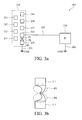
- FIG. 3a is a schematic diagram of an exemplary embodiment of a printed circuit board
- FIG. 3b is a schematic diagram of an exemplary embodiment of protrudent parts
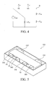
- FIG. 4 is an equivalent diagram of FIG. 3a ;
- FIG. 5 is a schematic diagram of an exemplary embodiment of a connector.
- FIG. 3a is a schematic diagram of an exemplary embodiment of a printed circuit board.
- Printed circuit board (PCB) 200 comprises a pad group 210, traces 220-222, and an IC 230.
- Pad group 210 comprises pads 211-219 for welding with a connector (not shown). When the pins of the connector is welded to pads 211-219, if a connection line is utilized for connecting an external peripheral device and the connector, data can be transmitted between the external peripheral device and IC 230.
- shapes of pads 211-219 are squares, but the disclosure is not limited thereto. In some embodiments, the shapes of pads 211-219 are circular or other shapes.
- Pad 219 receives a power signal, such as a grounding signal.
- Pad 218 receives a data signal.
- Pad 218 comprises a side adjoining pad 219.
- the side of pad 218 comprises protrudent part P1.
- Pad 219 comprises a side adjoining pad 218.
- the side of pad 219 comprises protrudent part P2.
- Protrudent part P1 faces and approaches protrudent part P2.
- the shapes of protrudent parts P1 and P2 are triangles, but are not limited to these.
- only pad 218 receiving the data signal comprises a protrudent part P1 facing pad 219.
- Pad 219 does not comprise protrudent part P2.
- only pad 219 receiving the power signal comprises protrudent part P2 and pad 218 receiving the data signal does not comprises protrudent part P1, wherein protrudent part P2 faces pad 218.
- FIG. 3b is a schematic diagram of an exemplary embodiment of protrudent parts.
- the side of pad 311, facing pad 312, comprises protrudent part P3.
- the side of pad 312, facing pad 311, comprises protrudent part P4.
- Protrudent part P3 faces and approaches protrudent part P4.
- protrudent parts P3 and P4 are arcs.
- FIG. 4 is an equivalent diagram of FIG. 3a .
- Symbol Z 41 represents the impedance of the first half of trace 220.
- Symbol Z 42 represents the impedance of the second half of trace 220.
- Symbol Z 43 represents the impedance of IC 230.
- Symbol Z 44 represents the impedance of trace 222.
- Symbol Z 45 represents the impedance between protrudent part P1 and the ground.
- V new Z 43 + Z 44 ⁇ I ESD ⁇ Z 45 Z 41 + Z 42 + Z 43 + Z 45
- impedances Z 23 and Z 24 equal to impedances Z 43 and Z 44 , respectively.
- voltage V new is less than voltage V gen .
- impedance Z 45 is reduced, thus, the electrostatic effect is reduced.
- Impedance Z 45 bases on the shapes of protrudent parts P1 and P2 and a distance between protrudent parts P1 and P2. Electrostatic tolerance of PCB 200 is controlled when protrudent parts P1 and P2 are controlled. Additionally, a region connecting pad 219 is paved with copper such that other pads may utilize peak discharge to release the electrostatic current to ground.
- FIG. 5 is a schematic diagram of an exemplary embodiment of a connector.
- Connector 500 comprises pins 510-560.
- pins 530 and 560 transmit power signals, such as grounding signals.
- Pins 540 and 550 transmit data signals.
- the right side of pin 550, approaching pin 560, comprises protrudent part P5 for releasing the electrostatic current.
- the side of pin 540, facing pin 530 comprises protrudent part P6.
- the side of pin 530, facing pin 540 comprises protrudent part P7.
Landscapes
- Engineering & Computer Science (AREA)
- Microelectronics & Electronic Packaging (AREA)
- Details Of Connecting Devices For Male And Female Coupling (AREA)
- Earth Drilling (AREA)
- Piezo-Electric Or Mechanical Vibrators, Or Delay Or Filter Circuits (AREA)
- Quick-Acting Or Multi-Walled Pipe Joints (AREA)
- Coupling Device And Connection With Printed Circuit (AREA)
Abstract
Description
- The invention relates to a connector and a printed circuit board (PCB), and more particularly to a connector and a PCB for discharging electrostatic stress.
-
FIG. 1 is a schematic diagram of a conventional printed circuit board. Printed circuit board (PCB) 100 comprises apad group 110, traces 120, 121, and an integrated circuit (IC) 130.Pad group 110 comprises pads 111-113 for welding with an input/output connector (not shown).Pad 112 electrically connectsIC 130 viatrace 120.Pad 113 is grounded. - Electrostatic charge is easily accumulated in human bodies due to friction or other causes. When a person having a large amount of electrostatic charge touches a cable connecting an input/output connector, the accumulated electrostatic charge enters
IC 130 frompad 112 andtrace 120. Thus,IC 130 is damaged. -
FIG. 2 is an equivalent diagram of the convention PCB. Symbol Z21 represents the impedance of the first half oftrace 120. The first half oftrace 120 approachespad group 110. Symbol Z22 represents the impedance of the second half oftrace 120. The second half of impedance oftrace 120 approachesIC 130. Symbol Z23 represents the impedance ofIC 130. Symbol Z24 represents the impedance oftrace 121. - When an electrostatic event occurs in
pad 112, electrostatic current IESD is generated. Voltage Vgen of point A is expressed by the following equation (1): -

- If the electrostatic charge entering from the outside is not properly taken care of, the ICs welded in the PCB are damaged. Thus, the computer comprising the damaged ICs crashes.
- Connectors are provided. An exemplary embodiment of a connector comprises a first pin and a second pin. The first pin comprises a first side comprising a first protrudent part. The second pin comprises a second side facing the first side. The first protrudent part approaches the second side.
- Printed circuit boards are also provided. An exemplary embodiment of a printed circuit board comprises a first pad and a second pad. The first pad comprises a first side comprising a first protrudent part. The second pad comprises a second side facing the first side. The first protrudent part approaches the second side
- A detailed description is given in the following embodiments with reference to the accompanying drawings.
- The invention can be more fully understood by referring to the following detailed description and examples with references made to the accompanying drawings, wherein:
-
FIG. 1 is a schematic diagram of a conventional printed circuit board; -
FIG. 2 is an equivalent diagram of the conventional printed circuit board; -
FIG. 3a is a schematic diagram of an exemplary embodiment of a printed circuit board; -
FIG. 3b is a schematic diagram of an exemplary embodiment of protrudent parts; -
FIG. 4 is an equivalent diagram ofFIG. 3a ; and -
FIG. 5 is a schematic diagram of an exemplary embodiment of a connector. - The following description is of the best-contemplated mode of carrying out the invention. This description is made for the purpose of illustrating the general principles of the invention and should not be taken in a limiting sense. The scope of the invention is best determined by reference to the appended claims.
-
FIG. 3a is a schematic diagram of an exemplary embodiment of a printed circuit board. Printed circuit board (PCB) 200 comprises apad group 210, traces 220-222, and anIC 230.Pad group 210 comprises pads 211-219 for welding with a connector (not shown). When the pins of the connector is welded to pads 211-219, if a connection line is utilized for connecting an external peripheral device and the connector, data can be transmitted between the external peripheral device andIC 230. In this embodiment, shapes of pads 211-219 are squares, but the disclosure is not limited thereto. In some embodiments, the shapes of pads 211-219 are circular or other shapes. -
Pad 219 receives a power signal, such as a grounding signal.Pad 218 receives a data signal.Pad 218 comprises aside adjoining pad 219. The side ofpad 218 comprises protrudent part P1.Pad 219 comprises aside adjoining pad 218. The side ofpad 219 comprises protrudent part P2. Protrudent part P1 faces and approaches protrudent part P2. In this embodiment, the shapes of protrudent parts P1 and P2 are triangles, but are not limited to these. In some embodiments, only pad 218 receiving the data signal comprises a protrudent partP1 facing pad 219.Pad 219 does not comprise protrudent part P2. In one embodiment, only pad 219 receiving the power signal comprises protrudent part P2 and pad 218 receiving the data signal does not comprises protrudent part P1, wherein protrudent part P2 facespad 218. -
FIG. 3b is a schematic diagram of an exemplary embodiment of protrudent parts. The side ofpad 311, facingpad 312, comprises protrudent part P3. The side ofpad 312, facingpad 311, comprises protrudent part P4. Protrudent part P3 faces and approaches protrudent part P4. In this embodiment, protrudent parts P3 and P4 are arcs. - Referring to
FIG. 3a , when a data signal is transmitted from an external peripheral device toIC 230 viapad 218, if an electrostatic event occurs inpad 218, the electrostatic current is released from protrudent parts P1, P2,pad 219, and trace 221 to ground. Since electrostatic current is immediately released by protrudent parts P1 and P2,trace 220 andIC 230 are not affected by the electrostatic current. -
FIG. 4 is an equivalent diagram ofFIG. 3a . Symbol Z41 represents the impedance of the first half oftrace 220. Symbol Z42 represents the impedance of the second half oftrace 220. Symbol Z43 represents the impedance ofIC 230. Symbol Z44 represents the impedance oftrace 222. Symbol Z45 represents the impedance between protrudent part P1 and the ground. - When an electrostatic event occurs in
pad 218, electrostatic current IESD is generated. Voltage Vnew of point B is expressed by the following equation (2): -

- Compared with equation (1), assuming impedances Z23 and Z24 equal to impedances Z43 and Z44, respectively. After calculating, voltage Vnew is less than voltage Vgen. Thus, the effect of the electrostatic event is reduced through protrudent parts P1 and P2 of
pads PCB 200 is controlled when protrudent parts P1 and P2 are controlled. Additionally, aregion connecting pad 219 is paved with copper such that other pads may utilize peak discharge to release the electrostatic current to ground. -
FIG. 5 is a schematic diagram of an exemplary embodiment of a connector.Connector 500 comprises pins 510-560. In this embodiment, pins 530 and 560 transmit power signals, such as grounding signals.Pins pin 550, approachingpin 560, comprises protrudent part P5 for releasing the electrostatic current. Additionally, the side ofpin 540, facingpin 530, comprises protrudent part P6. The side ofpin 530, facingpin 540, comprises protrudent part P7. When an electrostatic event occurs inpin 540, the electrostatic current is released via protrudent parts P6 and P7. - While the invention has been described by way of example and in terms of the preferred embodiments, it is to be understood that the invention is not limited to the disclosed embodiments. To the contrary, it is intended to cover various modifications and similar arrangements (as would be apparent to those skilled in the art). Therefore, the scope of the appended claims should be accorded the broadest interpretation so as to encompass all such modifications and similar arrangements.
Claims (16)
- A connector, comprising:a first pin comprising a first side comprising a first protrudent part; anda second pin comprising a second side facing the first side, wherein the first protrudent part approaches the second side.
- The connector as claimed in claim 1, wherein the second side comprises a second protrudent part approaching the first protrudent part.
- The connector as claimed in claim 2, wherein a data signal is transmitted by the first pin and a power signal is transmitted by the second pin.
- The connector as claimed in claim 3, wherein the power signal is a grounding signal.
- The connector as claimed in claim 2, wherein the shape of the first protrudent part is a first triangle and the shape of the second protrudent part is a second triangle.
- The connector as claimed in claim 5, wherein the peak of the first triangle approaches the peak of the second triangle.
- The connector as claimed in claim 2, wherein the shape of the first protrudent part is a first arc and the shape of the second protrudent part is a second arc.
- The connector as claimed in claim 7, wherein a terminal of the first arc approaches a terminal of the second arc.
- A printed circuit board, comprising:a first pad comprising a first side comprising a first protrudent part; anda second pad comprising a second side facing the first side, wherein the first protrudent part approaches the second side.
- The printed circuit board as claimed in claim 9, wherein the second side comprises a second protrudent part approaching the first protrudent part.
- The printed circuit board as claimed in claim 10, wherein a data signal is transmitted by the first pad and a power signal is transmitted by the second pad.
- The printed circuit board as claimed in claim 11, wherein the power signal is a grounding signal.
- The printed circuit board as claimed in claim 10, wherein the shape of the first protrudent part is a first triangle and the shape of the second protrudent part is a second triangle.
- The printed circuit board as claimed in claim 13, wherein the peak of the first triangle approaches the peak of the second triangle.
- The printed circuit board as claimed in claim 10, wherein the shape of the first protrudent part is a first arc and the shape of the second protrudent part is a second arc.
- The printed circuit board as claimed in claim 15, wherein a terminal of the first arc approaches a terminal of the second arc.
Priority Applications (3)
| Application Number | Priority Date | Filing Date | Title |
|---|---|---|---|
| AT07114688T ATE453938T1 (en) | 2007-08-21 | 2007-08-21 | CONNECTOR |
| EP07114688A EP2051339B1 (en) | 2007-08-21 | 2007-08-21 | Connector |
| DE602007004122T DE602007004122D1 (en) | 2007-08-21 | 2007-08-21 | Connectors |
Applications Claiming Priority (1)
| Application Number | Priority Date | Filing Date | Title |
|---|---|---|---|
| EP07114688A EP2051339B1 (en) | 2007-08-21 | 2007-08-21 | Connector |
Publications (2)
| Publication Number | Publication Date |
|---|---|
| EP2051339A1 true EP2051339A1 (en) | 2009-04-22 |
| EP2051339B1 EP2051339B1 (en) | 2009-12-30 |
Family
ID=38917865
Family Applications (1)
| Application Number | Title | Priority Date | Filing Date |
|---|---|---|---|
| EP07114688A Ceased EP2051339B1 (en) | 2007-08-21 | 2007-08-21 | Connector |
Country Status (3)
| Country | Link |
|---|---|
| EP (1) | EP2051339B1 (en) |
| AT (1) | ATE453938T1 (en) |
| DE (1) | DE602007004122D1 (en) |
Cited By (1)
| Publication number | Priority date | Publication date | Assignee | Title |
|---|---|---|---|---|
| EP2747216A1 (en) * | 2012-12-24 | 2014-06-25 | Alcatel Lucent | Connector with improved ESD protection |
Citations (4)
| Publication number | Priority date | Publication date | Assignee | Title |
|---|---|---|---|---|
| US6059983A (en) * | 1997-09-23 | 2000-05-09 | Hewlett-Packard Company | Method for fabricating an overcoated printed circuit board with contaminant-free areas |
| US6241537B1 (en) * | 2000-05-18 | 2001-06-05 | Palm, Inc. | ESD protective connector apparatus |
| EP1229618A2 (en) * | 2001-01-31 | 2002-08-07 | Kabushiki Kaisha Toshiba | Discharge gap apparatus |
| FR2831336A1 (en) * | 2001-10-18 | 2003-04-25 | Peugeot Citroen Automobiles Sa | Car diagnostic maintenance plug electrostatic protection having isolating support plate with earth/connection pins and metallic covering touching earth pin/surrounding voltage pin and having pointed electrostatic discharge sections. |
-
2007
- 2007-08-21 AT AT07114688T patent/ATE453938T1/en not_active IP Right Cessation
- 2007-08-21 DE DE602007004122T patent/DE602007004122D1/en active Active
- 2007-08-21 EP EP07114688A patent/EP2051339B1/en not_active Ceased
Patent Citations (4)
| Publication number | Priority date | Publication date | Assignee | Title |
|---|---|---|---|---|
| US6059983A (en) * | 1997-09-23 | 2000-05-09 | Hewlett-Packard Company | Method for fabricating an overcoated printed circuit board with contaminant-free areas |
| US6241537B1 (en) * | 2000-05-18 | 2001-06-05 | Palm, Inc. | ESD protective connector apparatus |
| EP1229618A2 (en) * | 2001-01-31 | 2002-08-07 | Kabushiki Kaisha Toshiba | Discharge gap apparatus |
| FR2831336A1 (en) * | 2001-10-18 | 2003-04-25 | Peugeot Citroen Automobiles Sa | Car diagnostic maintenance plug electrostatic protection having isolating support plate with earth/connection pins and metallic covering touching earth pin/surrounding voltage pin and having pointed electrostatic discharge sections. |
Cited By (1)
| Publication number | Priority date | Publication date | Assignee | Title |
|---|---|---|---|---|
| EP2747216A1 (en) * | 2012-12-24 | 2014-06-25 | Alcatel Lucent | Connector with improved ESD protection |
Also Published As
| Publication number | Publication date |
|---|---|
| EP2051339B1 (en) | 2009-12-30 |
| DE602007004122D1 (en) | 2010-02-11 |
| ATE453938T1 (en) | 2010-01-15 |
Similar Documents
| Publication | Publication Date | Title |
|---|---|---|
| US7064423B2 (en) | IC module and IC card | |
| EP1986297A2 (en) | Spark gaps for ESD protection | |
| US7666001B2 (en) | Circuit connection structure and printed circuit board | |
| US20130214794A1 (en) | Misalignment detection devices | |
| EP0849982A1 (en) | Improved transistor/resistor printed circuit board layout | |
| US8441273B2 (en) | Testing card and testing system for USB port | |
| CN111009223A (en) | Source driver and display device | |
| CN1963600A (en) | Liquid crystal display panel | |
| CN201114972Y (en) | Connectors and Circuit Boards | |
| US6185105B1 (en) | Discharge structure of printed circuit board | |
| US20090144474A1 (en) | Method and apparatus for providing an alternative power source for a graphics card | |
| CN101651133B (en) | On-membrane chip wiring method and structure for reducing electromagnetic interference | |
| CN100562210C (en) | circuit board combination | |
| CN109215558B (en) | Display device | |
| JP2002131333A (en) | Probe card | |
| CN111315124A (en) | Circuit board assembly and electronic device | |
| US20090035968A1 (en) | Connector and printed circuit board | |
| US7026545B2 (en) | Flex cable having a return-signal path and method for reducing length and impedance of a return-signal path | |
| CN113179579A (en) | Circuit board and electronic equipment | |
| US20240341028A1 (en) | Circuit board module and touch display apparatus | |
| EP2051339B1 (en) | Connector | |
| JP3138624U (en) | Connectors and printed circuit boards | |
| US7192305B2 (en) | Electronic apparatus including restraint member receiving plug coupled to connector | |
| CN106413234A (en) | Electrostatic discharge protection structure and electronic device | |
| US20230246353A1 (en) | Dual-path high-speed interconnect pcb layout solution |
Legal Events
| Date | Code | Title | Description |
|---|---|---|---|
| PUAI | Public reference made under article 153(3) epc to a published international application that has entered the european phase |
Free format text: ORIGINAL CODE: 0009012 |
|
| 17P | Request for examination filed |
Effective date: 20080704 |
|
| AK | Designated contracting states |
Kind code of ref document: A1 Designated state(s): AT BE BG CH CY CZ DE DK EE ES FI FR GB GR HU IE IS IT LI LT LU LV MC MT NL PL PT RO SE SI SK TR |
|
| AX | Request for extension of the european patent |
Extension state: AL BA HR MK RS |
|
| GRAP | Despatch of communication of intention to grant a patent |
Free format text: ORIGINAL CODE: EPIDOSNIGR1 |
|
| RTI1 | Title (correction) |
Free format text: CONNECTOR |
|
| GRAS | Grant fee paid |
Free format text: ORIGINAL CODE: EPIDOSNIGR3 |
|
| GRAA | (expected) grant |
Free format text: ORIGINAL CODE: 0009210 |
|
| AK | Designated contracting states |
Kind code of ref document: B1 Designated state(s): AT BE BG CH CY CZ DE DK EE ES FI FR GB GR HU IE IS IT LI LT LU LV MC MT NL PL PT RO SE SI SK TR |
|
| REG | Reference to a national code |
Ref country code: GB Ref legal event code: FG4D |
|
| REG | Reference to a national code |
Ref country code: CH Ref legal event code: EP |
|
| REG | Reference to a national code |
Ref country code: IE Ref legal event code: FG4D |
|
| REF | Corresponds to: |
Ref document number: 602007004122 Country of ref document: DE Date of ref document: 20100211 Kind code of ref document: P |
|
| PG25 | Lapsed in a contracting state [announced via postgrant information from national office to epo] |
Ref country code: FI Free format text: LAPSE BECAUSE OF FAILURE TO SUBMIT A TRANSLATION OF THE DESCRIPTION OR TO PAY THE FEE WITHIN THE PRESCRIBED TIME-LIMIT Effective date: 20091230 Ref country code: SE Free format text: LAPSE BECAUSE OF FAILURE TO SUBMIT A TRANSLATION OF THE DESCRIPTION OR TO PAY THE FEE WITHIN THE PRESCRIBED TIME-LIMIT Effective date: 20091230 Ref country code: LT Free format text: LAPSE BECAUSE OF FAILURE TO SUBMIT A TRANSLATION OF THE DESCRIPTION OR TO PAY THE FEE WITHIN THE PRESCRIBED TIME-LIMIT Effective date: 20091230 |
|
| REG | Reference to a national code |
Ref country code: NL Ref legal event code: VDEP Effective date: 20091230 |
|
| LTIE | Lt: invalidation of european patent or patent extension |
Effective date: 20091230 |
|
| PG25 | Lapsed in a contracting state [announced via postgrant information from national office to epo] |
Ref country code: SI Free format text: LAPSE BECAUSE OF FAILURE TO SUBMIT A TRANSLATION OF THE DESCRIPTION OR TO PAY THE FEE WITHIN THE PRESCRIBED TIME-LIMIT Effective date: 20091230 Ref country code: LV Free format text: LAPSE BECAUSE OF FAILURE TO SUBMIT A TRANSLATION OF THE DESCRIPTION OR TO PAY THE FEE WITHIN THE PRESCRIBED TIME-LIMIT Effective date: 20091230 Ref country code: PL Free format text: LAPSE BECAUSE OF FAILURE TO SUBMIT A TRANSLATION OF THE DESCRIPTION OR TO PAY THE FEE WITHIN THE PRESCRIBED TIME-LIMIT Effective date: 20091230 |
|
| PG25 | Lapsed in a contracting state [announced via postgrant information from national office to epo] |
Ref country code: AT Free format text: LAPSE BECAUSE OF FAILURE TO SUBMIT A TRANSLATION OF THE DESCRIPTION OR TO PAY THE FEE WITHIN THE PRESCRIBED TIME-LIMIT Effective date: 20091230 |
|
| PG25 | Lapsed in a contracting state [announced via postgrant information from national office to epo] |
Ref country code: BG Free format text: LAPSE BECAUSE OF FAILURE TO SUBMIT A TRANSLATION OF THE DESCRIPTION OR TO PAY THE FEE WITHIN THE PRESCRIBED TIME-LIMIT Effective date: 20100330 Ref country code: RO Free format text: LAPSE BECAUSE OF FAILURE TO SUBMIT A TRANSLATION OF THE DESCRIPTION OR TO PAY THE FEE WITHIN THE PRESCRIBED TIME-LIMIT Effective date: 20091230 Ref country code: NL Free format text: LAPSE BECAUSE OF FAILURE TO SUBMIT A TRANSLATION OF THE DESCRIPTION OR TO PAY THE FEE WITHIN THE PRESCRIBED TIME-LIMIT Effective date: 20091230 Ref country code: EE Free format text: LAPSE BECAUSE OF FAILURE TO SUBMIT A TRANSLATION OF THE DESCRIPTION OR TO PAY THE FEE WITHIN THE PRESCRIBED TIME-LIMIT Effective date: 20091230 Ref country code: IS Free format text: LAPSE BECAUSE OF FAILURE TO SUBMIT A TRANSLATION OF THE DESCRIPTION OR TO PAY THE FEE WITHIN THE PRESCRIBED TIME-LIMIT Effective date: 20100430 Ref country code: PT Free format text: LAPSE BECAUSE OF FAILURE TO SUBMIT A TRANSLATION OF THE DESCRIPTION OR TO PAY THE FEE WITHIN THE PRESCRIBED TIME-LIMIT Effective date: 20100430 Ref country code: ES Free format text: LAPSE BECAUSE OF FAILURE TO SUBMIT A TRANSLATION OF THE DESCRIPTION OR TO PAY THE FEE WITHIN THE PRESCRIBED TIME-LIMIT Effective date: 20100410 |
|
| PG25 | Lapsed in a contracting state [announced via postgrant information from national office to epo] |
Ref country code: CZ Free format text: LAPSE BECAUSE OF FAILURE TO SUBMIT A TRANSLATION OF THE DESCRIPTION OR TO PAY THE FEE WITHIN THE PRESCRIBED TIME-LIMIT Effective date: 20091230 Ref country code: SK Free format text: LAPSE BECAUSE OF FAILURE TO SUBMIT A TRANSLATION OF THE DESCRIPTION OR TO PAY THE FEE WITHIN THE PRESCRIBED TIME-LIMIT Effective date: 20091230 Ref country code: BE Free format text: LAPSE BECAUSE OF FAILURE TO SUBMIT A TRANSLATION OF THE DESCRIPTION OR TO PAY THE FEE WITHIN THE PRESCRIBED TIME-LIMIT Effective date: 20091230 |
|
| PG25 | Lapsed in a contracting state [announced via postgrant information from national office to epo] |
Ref country code: CY Free format text: LAPSE BECAUSE OF FAILURE TO SUBMIT A TRANSLATION OF THE DESCRIPTION OR TO PAY THE FEE WITHIN THE PRESCRIBED TIME-LIMIT Effective date: 20091230 Ref country code: GR Free format text: LAPSE BECAUSE OF FAILURE TO SUBMIT A TRANSLATION OF THE DESCRIPTION OR TO PAY THE FEE WITHIN THE PRESCRIBED TIME-LIMIT Effective date: 20100331 |
|
| PLBE | No opposition filed within time limit |
Free format text: ORIGINAL CODE: 0009261 |
|
| STAA | Information on the status of an ep patent application or granted ep patent |
Free format text: STATUS: NO OPPOSITION FILED WITHIN TIME LIMIT |
|
| 26N | No opposition filed |
Effective date: 20101001 |
|
| PG25 | Lapsed in a contracting state [announced via postgrant information from national office to epo] |
Ref country code: DK Free format text: LAPSE BECAUSE OF FAILURE TO SUBMIT A TRANSLATION OF THE DESCRIPTION OR TO PAY THE FEE WITHIN THE PRESCRIBED TIME-LIMIT Effective date: 20091230 |
|
| PG25 | Lapsed in a contracting state [announced via postgrant information from national office to epo] |
Ref country code: MC Free format text: LAPSE BECAUSE OF NON-PAYMENT OF DUE FEES Effective date: 20100831 Ref country code: IT Free format text: LAPSE BECAUSE OF FAILURE TO SUBMIT A TRANSLATION OF THE DESCRIPTION OR TO PAY THE FEE WITHIN THE PRESCRIBED TIME-LIMIT Effective date: 20091230 |
|
| PG25 | Lapsed in a contracting state [announced via postgrant information from national office to epo] |
Ref country code: IE Free format text: LAPSE BECAUSE OF NON-PAYMENT OF DUE FEES Effective date: 20100821 |
|
| PG25 | Lapsed in a contracting state [announced via postgrant information from national office to epo] |
Ref country code: MT Free format text: LAPSE BECAUSE OF FAILURE TO SUBMIT A TRANSLATION OF THE DESCRIPTION OR TO PAY THE FEE WITHIN THE PRESCRIBED TIME-LIMIT Effective date: 20091230 |
|
| REG | Reference to a national code |
Ref country code: CH Ref legal event code: PL |
|
| PG25 | Lapsed in a contracting state [announced via postgrant information from national office to epo] |
Ref country code: LI Free format text: LAPSE BECAUSE OF NON-PAYMENT OF DUE FEES Effective date: 20110831 Ref country code: CH Free format text: LAPSE BECAUSE OF NON-PAYMENT OF DUE FEES Effective date: 20110831 |
|
| PG25 | Lapsed in a contracting state [announced via postgrant information from national office to epo] |
Ref country code: LU Free format text: LAPSE BECAUSE OF NON-PAYMENT OF DUE FEES Effective date: 20100821 Ref country code: HU Free format text: LAPSE BECAUSE OF FAILURE TO SUBMIT A TRANSLATION OF THE DESCRIPTION OR TO PAY THE FEE WITHIN THE PRESCRIBED TIME-LIMIT Effective date: 20100701 |
|
| PG25 | Lapsed in a contracting state [announced via postgrant information from national office to epo] |
Ref country code: TR Free format text: LAPSE BECAUSE OF FAILURE TO SUBMIT A TRANSLATION OF THE DESCRIPTION OR TO PAY THE FEE WITHIN THE PRESCRIBED TIME-LIMIT Effective date: 20091230 |
|
| REG | Reference to a national code |
Ref country code: FR Ref legal event code: PLFP Year of fee payment: 10 |
|
| REG | Reference to a national code |
Ref country code: FR Ref legal event code: PLFP Year of fee payment: 11 |
|
| REG | Reference to a national code |
Ref country code: FR Ref legal event code: PLFP Year of fee payment: 12 |
|
| PGFP | Annual fee paid to national office [announced via postgrant information from national office to epo] |
Ref country code: DE Payment date: 20200812 Year of fee payment: 14 Ref country code: FR Payment date: 20200715 Year of fee payment: 14 Ref country code: GB Payment date: 20200813 Year of fee payment: 14 |
|
| REG | Reference to a national code |
Ref country code: DE Ref legal event code: R119 Ref document number: 602007004122 Country of ref document: DE |
|
| GBPC | Gb: european patent ceased through non-payment of renewal fee |
Effective date: 20210821 |
|
| PG25 | Lapsed in a contracting state [announced via postgrant information from national office to epo] |
Ref country code: GB Free format text: LAPSE BECAUSE OF NON-PAYMENT OF DUE FEES Effective date: 20210821 Ref country code: FR Free format text: LAPSE BECAUSE OF NON-PAYMENT OF DUE FEES Effective date: 20210831 Ref country code: DE Free format text: LAPSE BECAUSE OF NON-PAYMENT OF DUE FEES Effective date: 20220301 |