EP2051312A2 - Organic light emitting device and color display apparatus using the same - Google Patents
Organic light emitting device and color display apparatus using the same Download PDFInfo
- Publication number
- EP2051312A2 EP2051312A2 EP08158039A EP08158039A EP2051312A2 EP 2051312 A2 EP2051312 A2 EP 2051312A2 EP 08158039 A EP08158039 A EP 08158039A EP 08158039 A EP08158039 A EP 08158039A EP 2051312 A2 EP2051312 A2 EP 2051312A2
- Authority
- EP
- European Patent Office
- Prior art keywords
- oled
- emls
- optical path
- path control
- color
- Prior art date
- Legal status (The legal status is an assumption and is not a legal conclusion. Google has not performed a legal analysis and makes no representation as to the accuracy of the status listed.)
- Withdrawn
Links
- 230000003287 optical effect Effects 0.000 claims abstract description 95
- 239000000758 substrate Substances 0.000 claims description 17
- 239000003086 colorant Substances 0.000 claims description 12
- 239000000463 material Substances 0.000 claims description 10
- 229910052751 metal Inorganic materials 0.000 claims description 10
- 239000002184 metal Substances 0.000 claims description 10
- MCMNRKCIXSYSNV-UHFFFAOYSA-N Zirconium dioxide Chemical compound O=[Zr]=O MCMNRKCIXSYSNV-UHFFFAOYSA-N 0.000 claims description 6
- 230000005525 hole transport Effects 0.000 claims description 5
- 238000002834 transmittance Methods 0.000 claims description 5
- 230000000295 complement effect Effects 0.000 claims description 4
- 229910052581 Si3N4 Inorganic materials 0.000 claims description 3
- PNEYBMLMFCGWSK-UHFFFAOYSA-N aluminium oxide Inorganic materials [O-2].[O-2].[O-2].[Al+3].[Al+3] PNEYBMLMFCGWSK-UHFFFAOYSA-N 0.000 claims description 3
- QVQLCTNNEUAWMS-UHFFFAOYSA-N barium oxide Inorganic materials [Ba]=O QVQLCTNNEUAWMS-UHFFFAOYSA-N 0.000 claims description 3
- 229910052593 corundum Inorganic materials 0.000 claims description 3
- CJNBYAVZURUTKZ-UHFFFAOYSA-N hafnium(IV) oxide Inorganic materials O=[Hf]=O CJNBYAVZURUTKZ-UHFFFAOYSA-N 0.000 claims description 3
- CPLXHLVBOLITMK-UHFFFAOYSA-N magnesium oxide Inorganic materials [Mg]=O CPLXHLVBOLITMK-UHFFFAOYSA-N 0.000 claims description 3
- 229910001845 yogo sapphire Inorganic materials 0.000 claims description 3
- 239000010410 layer Substances 0.000 description 121
- 230000000052 comparative effect Effects 0.000 description 17
- 238000010586 diagram Methods 0.000 description 15
- 238000005094 computer simulation Methods 0.000 description 14
- 238000000295 emission spectrum Methods 0.000 description 12
- 238000001228 spectrum Methods 0.000 description 12
- 239000012044 organic layer Substances 0.000 description 5
- 230000008859 change Effects 0.000 description 4
- 238000000034 method Methods 0.000 description 4
- 238000004088 simulation Methods 0.000 description 4
- 238000002347 injection Methods 0.000 description 3
- 239000007924 injection Substances 0.000 description 3
- 238000004519 manufacturing process Methods 0.000 description 3
- 230000008569 process Effects 0.000 description 3
- 238000010521 absorption reaction Methods 0.000 description 2
- 230000000903 blocking effect Effects 0.000 description 2
- 230000000694 effects Effects 0.000 description 2
- 239000008393 encapsulating agent Substances 0.000 description 2
- 239000000945 filler Substances 0.000 description 2
- 239000011521 glass Substances 0.000 description 2
- AMGQUBHHOARCQH-UHFFFAOYSA-N indium;oxotin Chemical compound [In].[Sn]=O AMGQUBHHOARCQH-UHFFFAOYSA-N 0.000 description 2
- 239000010409 thin film Substances 0.000 description 2
- 239000011248 coating agent Substances 0.000 description 1
- 238000000576 coating method Methods 0.000 description 1
- 238000010276 construction Methods 0.000 description 1
- 238000005137 deposition process Methods 0.000 description 1
- 239000011159 matrix material Substances 0.000 description 1
- 230000004044 response Effects 0.000 description 1
- 239000000243 solution Substances 0.000 description 1
- YVTHLONGBIQYBO-UHFFFAOYSA-N zinc indium(3+) oxygen(2-) Chemical compound [O--].[Zn++].[In+3] YVTHLONGBIQYBO-UHFFFAOYSA-N 0.000 description 1
Images


Classifications
-
- H—ELECTRICITY
- H10—SEMICONDUCTOR DEVICES; ELECTRIC SOLID-STATE DEVICES NOT OTHERWISE PROVIDED FOR
- H10K—ORGANIC ELECTRIC SOLID-STATE DEVICES
- H10K50/00—Organic light-emitting devices
- H10K50/80—Constructional details
- H10K50/85—Arrangements for extracting light from the devices
- H10K50/852—Arrangements for extracting light from the devices comprising a resonant cavity structure, e.g. Bragg reflector pair
-
- H—ELECTRICITY
- H05—ELECTRIC TECHNIQUES NOT OTHERWISE PROVIDED FOR
- H05B—ELECTRIC HEATING; ELECTRIC LIGHT SOURCES NOT OTHERWISE PROVIDED FOR; CIRCUIT ARRANGEMENTS FOR ELECTRIC LIGHT SOURCES, IN GENERAL
- H05B33/00—Electroluminescent light sources
- H05B33/12—Light sources with substantially two-dimensional radiating surfaces
- H05B33/26—Light sources with substantially two-dimensional radiating surfaces characterised by the composition or arrangement of the conductive material used as an electrode
- H05B33/28—Light sources with substantially two-dimensional radiating surfaces characterised by the composition or arrangement of the conductive material used as an electrode of translucent electrodes
-
- H—ELECTRICITY
- H05—ELECTRIC TECHNIQUES NOT OTHERWISE PROVIDED FOR
- H05B—ELECTRIC HEATING; ELECTRIC LIGHT SOURCES NOT OTHERWISE PROVIDED FOR; CIRCUIT ARRANGEMENTS FOR ELECTRIC LIGHT SOURCES, IN GENERAL
- H05B33/00—Electroluminescent light sources
- H05B33/12—Light sources with substantially two-dimensional radiating surfaces
- H05B33/14—Light sources with substantially two-dimensional radiating surfaces characterised by the chemical or physical composition or the arrangement of the electroluminescent material, or by the simultaneous addition of the electroluminescent material in or onto the light source
-
- H—ELECTRICITY
- H05—ELECTRIC TECHNIQUES NOT OTHERWISE PROVIDED FOR
- H05B—ELECTRIC HEATING; ELECTRIC LIGHT SOURCES NOT OTHERWISE PROVIDED FOR; CIRCUIT ARRANGEMENTS FOR ELECTRIC LIGHT SOURCES, IN GENERAL
- H05B33/00—Electroluminescent light sources
- H05B33/12—Light sources with substantially two-dimensional radiating surfaces
- H05B33/22—Light sources with substantially two-dimensional radiating surfaces characterised by the chemical or physical composition or the arrangement of auxiliary dielectric or reflective layers
-
- H—ELECTRICITY
- H10—SEMICONDUCTOR DEVICES; ELECTRIC SOLID-STATE DEVICES NOT OTHERWISE PROVIDED FOR
- H10K—ORGANIC ELECTRIC SOLID-STATE DEVICES
- H10K50/00—Organic light-emitting devices
- H10K50/10—OLEDs or polymer light-emitting diodes [PLED]
- H10K50/19—Tandem OLEDs
-
- H—ELECTRICITY
- H10—SEMICONDUCTOR DEVICES; ELECTRIC SOLID-STATE DEVICES NOT OTHERWISE PROVIDED FOR
- H10K—ORGANIC ELECTRIC SOLID-STATE DEVICES
- H10K59/00—Integrated devices, or assemblies of multiple devices, comprising at least one organic light-emitting element covered by group H10K50/00
- H10K59/80—Constructional details
- H10K59/875—Arrangements for extracting light from the devices
- H10K59/876—Arrangements for extracting light from the devices comprising a resonant cavity structure, e.g. Bragg reflector pair
-
- H—ELECTRICITY
- H10—SEMICONDUCTOR DEVICES; ELECTRIC SOLID-STATE DEVICES NOT OTHERWISE PROVIDED FOR
- H10K—ORGANIC ELECTRIC SOLID-STATE DEVICES
- H10K50/00—Organic light-emitting devices
- H10K50/10—OLEDs or polymer light-emitting diodes [PLED]
- H10K50/11—OLEDs or polymer light-emitting diodes [PLED] characterised by the electroluminescent [EL] layers
- H10K50/125—OLEDs or polymer light-emitting diodes [PLED] characterised by the electroluminescent [EL] layers specially adapted for multicolour light emission, e.g. for emitting white light
Landscapes
- Physics & Mathematics (AREA)
- Optics & Photonics (AREA)
- Electroluminescent Light Sources (AREA)
Abstract
Description
- In an organic light emitting device (OLED), holes from an anode combine with electrons from a cathode in an organic emission layer (EML) formed between the anode and the cathode to emit light, thereby forming an image. Since the OLED has excellent display characteristics, such as a wide viewing angle, a faster response speed, a smaller thickness, a lower fabrication cost, and a higher contrast, the OLED has attracted much attention as an advanced flat panel display device.
- In general, the OLED may have a multilayered structure in order to improve luminous efficiency. For example, a hole injection layer (HIL) and a hole transport layer (HTL) may be further formed between an anode and an organic EML, and an electron injection layer (EIL) and an electron transport layer (ETL) may be further formed between a cathode and the organic EML. Also, other additional layers may be further formed.
- The OLED may emit light in a desired color by forming the organic EML using an appropriate material. Based on this principle, it is possible to embody a color display apparatus using the OLED. For example, in a color display apparatus using an OLED, each of pixels may include a sub-pixel having a red (R) organic EML, a sub-pixel having a green (G) organic EML, and a sub-pixel having a blue (B) organic EML. When different organic EMLs are formed in respective sub-pixels, however, it is difficult to embody large-area high-resolution display apparatuses due to a complicated fabrication process.
- In order to overcome the drawback, a white OLED has been proposed. The white OLED may be embodied by forming a plurality of organic emission materials for emitting light in R, G, and B colors in an organic EML or forming two or more pairs of organic emission materials for emitting light in complementary colors. The white OLED creates colors using color filters. In this case, since all sub-pixels include organic EMLs with the same structure, fabricating large-area high-resolution display apparatuses is relatively easy.
- Meanwhile, OLEDs may be classified into bottom-emission OLEDs and top-emission OLEDs depending on a direction in which light is emitted from an organic EML. In a bottom-emission OLED, light is extracted to a bottom surface of the OLED on which a thin film transistor (TFT) for driving the OLED is disposed. In a top-emission OLED, a reflective electrode is disposed under an organic EML so that light is extracted to an upper portion of a TFT. Typically, since the top-emission OLED may increase an emission area (or aperture ratio) more than the bottom-emission OLED, the top-emission OLED is more suited for high-resolution OLEDs.
- In the top-emission OLED, however, resonant cavities are formed between a reflective electrode disposed under an organic EML and a semi-transmissive electrode disposed on the organic EML. Since resonance caused in the resonant cavities narrows the spectrum of externally emitted light, it is advantageous at extracting only light with a specific wavelength, but it is disadvantageous at extracting white light. Also, a top-emission white OLED using color filters narrows a color gamut and increases a variation of color with a viewing angle.
- In order to solve this problem, an OLED for extracting only light with a specific wavelength using a single resonator mode has been proposed. In this case, however, the optical thickness of resonant cavities should be varied according to the wavelength of light. Therefore, fabrication of a color display apparatus using the OLED may involve a very complicated process so that the optical thickness of the resonant cavities may be controlled to be different according to respective R, G, and B sub-pixels.
- It is therefore one object of the present invention to provide an improved top-emission or bottom-emission organic light emitting display (OLED) that is free of the disadvantages above.
- It is another object for the present invention to provide a top-emission or bottom-emission organic light emitting display (OLED) using color filters, in which has a wide color gamut and reduces a variation of color with a viewing angle.
- It is still another object for the present invention to provide a color display apparatus using the above-described OLED.
- According to an aspect of the present invention, there is provided an OLED including a reflective electrode and a transmissive or semi-transmissive electrode disposed opposite each other; at least two organic emission layers (EMLs) interposed between the reflective electrode and the transmissive or semi-transmissive electrode; and an optical path control layer prepared on an outer surface of the transmissive or semi-transmissive electrode. In the OLED, a resonator is formed between the reflective electrode and the optical path control layer so that a resonance mode of light extracted from the optical path control layer is a multi-resonance mode having at least two modes in a visible light region. A distance between the organic EMLs satisfies the condition of constructive interference between light beams emitted by the respective organic EMLs.
- The at least two organic EMLs may be white EMLs, each of which includes a red (R) EML, a green (G) EML, and a blue (B) EML.
- The at least two organic EMLs may be white EMLs, each of which includes two kinds of single-color or multi-color EMLs that emit light in complementary colors.
- Each of distances between the EMLs of the at least two organic EMLs that emit light in the same color may satisfy the condition of the constructive interference.
- A distance between the EMLs of at least two organic EMLs that emit light in the same color may be greater than a distance that permits center wavelength of a blue color to satisfy the condition of the constructive interference.
- A distance between the EMLs of at least two organic EMLs that emit light in the same color may be within ± 10% of a distance that permits center wavelength of the blue color to satisfy the condition of the constructive interference.
- The at least two organic EMLs may be single-color EMLs that emit light in the same color.
- The OLED may further include a PN junction layer interposed between the at least two organic EMLs.
- The PN junction layer may include an n-doped electron transport layer (ETL) and a p-doped hole transport layer (HTL).
- The optical path control layer may be formed of a material having an optical transmittance of 90% or higher in the visible light region.
- The optical path control layer may have a refractive index of about 1.6 to 2.6.
- The optical path control layer may be formed of at least one selected from the group consisting of Al2O3, BaO, MgO, HfO2, ZrO2, CaO2, SrO2, Y2O3, Si3N4, AIN, GaN, ZnS, and CdS.
- The optical path control layer may have a thickness of about 300 nm to 900 nm. The reflectance of the transmissive or semi-transmissive electrode may range from 0.1 to 50%.
- The transmissive or semi-transmissive electrode may be formed using one of a thin metal layer and a transparent conductive oxide.
- The OLED may further include a multiple dielectric mirror layer disposed on a top surface of the optical path control layer. The multiple dielectric mirror layer may be formed alternating a high-refractive index dielectric layer and a low-refractive index dielectric layer.
- The OLED may further include a thin metal mirror layer disposed on a top surface of the optical path control layer.
- According to another aspect of the present invention, there is provided a color display apparatus including a reflective electrode and a transmissive or semi-transmissive electrode disposed opposite each other; at least two organic EMLs interposed between the reflective electrode and the transmissive or semi-transmissive electrode; an optical path control layer disposed on an outer surface of the transmissive or semi-transmissive electrode; a transparent substrate disposed opposite the optical path control layer; and a plurality of color filters disposed on a surface of the transparent substrate. Resonators are respectively formed between the reflective electrodes and the optical path control layer so that a resonance mode of light extracted from the optical path control layer is a multi-resonance mode having at least two modes in a visible light region. Also, a distance between the organic EMLs satisfies the condition for constructive interference between light beams emitted by the respective organic EMLs, and the condition of constructive interference satisfying an equation as follows:

where njλ denotes a reflective index of a j-th layer of the white OLED with respect to a predetermined light wavelength λ, dj denotes a thickness of the j-th layer of the white OLED, δj denotes a phase change caused when light passes through the j-th layer and when the light is reflected by the optical path control layer, the transmissive or semi-transmissive electrode, and the reflective electrode, and q denotes an arbitrary integral number. - A more complete appreciation of the invention, and many of the attendant advantages thereof, will be readily apparent as the same becomes better understood by reference to the following detailed description when considered in conjunction with the accompanying drawings in which like reference symbols indicate the same or similar components, wherein:
-
FIG. 1 is a schematic view of a top-emitting white organic light emitting display (OLED) constructed as an embodiment of the present invention; -
FIG. 2 is a schematic view of a white OLED according to a comparative example; -
FIG. 3 is a detailed schematic view of a top-emitting white OLED constructed as an embodiment of the present invention; -
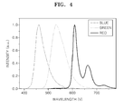
FIG. 4 is a two dimensional graph showing red(R)/blue(B)/green(G) spectra used for a simulation according to the present invention; -
FIG. 5 is a two dimensional graph showing transmissive spectra of color filers used for a simulation according to the present invention; -
FIG. 6 is a chromaticity diagram showing a color reproduction range, which is measured by comparing chromaticity coordinates calculated using the spectra ofFIG. 4 and the transmittances of color filters ofFIG. 5 with National Television Standards Committee (NTSC) chromaticity coordinates; -
FIG. 7 is a two dimensional graph of simulation results showing an emission spectrum relative to a viewing angle according to the comparative example shown inFIG. 2 ; -
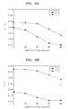
FIG. 8A is a two dimensional graph showing chromaticity coordinates relative to a viewing angle in the white OLED according to the comparative example shown inFIG. 2 ; -
FIG. 8B is a two dimensional graph showing the chromaticity coordinates relative to the viewing angle with respect to values u', v' and in the white OLED according to the comparative example shown inFIG. 2 ; -
FIG. 8C is a two dimensional graph showing the deviation of a value u'v' relative to a viewing angle from a front view in the white OLED according to the comparative example shown inFIG. 2 ; -
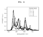
FIG. 9 is a two dimensional graph of simulation results showing an emission spectrum relative to a viewing angle in the top-emitting white OLED shown inFIG. 3 ; -
FIG. 10A is a two dimensional graph showing chromaticity coordinates relative to a viewing angle in the top-emitting white OLED shown inFIG. 3 ; -
FIG. 10B is a two dimensional graph showing the chromaticity coordinates relative to the viewing angle with respect to values u' and v' in the top-emitting white OLED shown inFIG. 3 ; -
FIG. 10C is a two dimensional graph showing the deviation of a value u'v' relative to a viewing angle from the front view in the top-emitting white OLED shown inFIG. 3 ; -
FIG. 11A is a two dimensional graph showing chromaticity coordinates relative to a viewing angle when white light is transmitted through an R color filter ofFIG. 5 in the top-emitting white OLED shown inFIG. 3 ; -
FIG. 11B is a two dimensional graph showing chromaticity coordinates relative to a viewing angle when white light is transmitted through a G color filter ofFIG. 5 in the top-emitting white OLED shown inFIG. 3 ; -
FIG. 11C is a two dimensional graph showing chromaticity coordinates relative to a viewing angle when white light is transmitted through a B color filter ofFIG. 5 in the top-emitting white OLED shown inFIG. 3 ; -
FIG. 11D is a two dimensional graph showing chromaticity coordinates relative to a viewing angle for white light when the white light is transmitted through all color filters ofFIG. 5 in the top-emitting white OLED shown inFIG. 3 ; -
FIG. 12A is a two dimensional graph showing the deviation of a value u'v' relative to a viewing angle when white light is transmitted through the R color filter ofFIG. 5 in the top-emitting white OLED shown inFIG. 3 ; -
FIG. 12B is a two dimensional graph showing the deviation of a value u'v' relative to a viewing angle when white light is transmitted through the G color filter ofFIG. 5 in the top-emitting white OLED shown inFIG. 3 ; -
FIG. 12C is a two dimensional graph showing the deviation of a value u'v' relative to a viewing angle when white light is transmitted through the B color filter ofFIG. 5 in the top-emitting white OLED shown inFIG. 3 ; -
FIG. 12D is a two dimensional graph showing the deviation of a value u'v' relative to a viewing angle for white light when the white light is transmitted through all the color filters ofFIG. 5 in the top-emitting white OLED shown inFIG. 3 ; and -
FIG. 13 is a cross-sectional view of a color display apparatus using the white OLED ofFIG. 1 , constructed as an embodiment of the present invention. - The present invention will be described more fully hereinafter with reference to the accompanying drawings, in which exemplary embodiments of the invention are shown. The same reference numerals are used to denote the same elements throughout the specification. In the drawings, the thicknesses of layers and regions are exaggerated for clarity. Although a top-emitting organic light emitting display (OLED) is exemplarily illustrated in the drawings, the present invention is not limited to the top-emitting OLED and can be also applied to a bottom-emitting OLED.
-
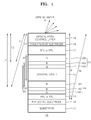
FIG. 1 is a schematic view of a top-emittingwhite OLED 10 constructed as an embodiment of the present invention. - Referring to
FIG. 1 , top-emittingwhite OLED 10 includes asubstrate 11, areflective electrode 12, atransmissive electrode 18, at least two organic emission layers (EMLs) 14 and 16 disposed betweenreflective electrode 12 andtransmissive electrode 18, layers 13, 15, and 17 for emitting electrons and holes to organic EMLs 14 and 16, and an optical path controllayer 19 disposed on an outer surface oftransmissive electrode 18.Substrate 11 may be, for example, a glass substrate. A thin film transistor (TFT) (not shown) may be prepared onsubstrate 11 in order to control the operation ofOLED 10.Transmissive electrode 18 may be formed of a transparent conductive oxide (TCO), such as indium tin oxide (ITO) or indium zinc oxide (IZO).Transmissive electrode 18, however, may be replaced by a semi-transmissive electrode obtained by coating a thin metal layer. -
Reflective electrode 12 may be an anode andtransmissive electrode 18 may be a cathode. Alternatively,reflective electrode 12 may be a cathode andtransmissive electrode 18 may be an anode. Whenreflective electrode 12 is an anode andtransmissive electrode 18 is a cathode,layer 13 interposed betweenreflective electrode 12 andfirst EML 14 may be a hole transport layer (HTL), andlayer 17 interposed betweentransmissive electrode 18 andsecond EML 16 may be an electron transport layer (ETL). Conversely,layer 13 interposed betweenreflective electrode 12 andfirst EML 14 may be an ETL, andlayer 17 interposed betweentransmissive electrode 18 andsecond EML 16 may be an HTL. Also, anorganic layer 15 may be further disposed between first and second EMLs 14 and 16 to control a distance between first and second EMLs 14 and 16. - Furthermore, first and second EMLs 14 and 16 may have various structures to create white light. For example, as shown in
FIG. 1 ,first EML 14 may include a red (R)EML 14R, a blue (B)EML 14B, and a green (G)EML 14G, andsecond EML 16 may include anR EML 16R, aB EML 16B, and aG EML 16G. Each of first and second EMLs 14 and 16, however, may be formed of two or more emission materials that emit light in complementary colors. - In general, an optical mode of light extracted from the OLED should be a multi-mode by generating multi-resonance in the OLED so that the white OLED can create high-quality white light and have a wide color gamut. Also, the variation of an optical mode due to a difference in an optical path relative to a viewing angle should be minimized so that the white OLED can have a wide color gamut and reduce a variation of color in a wide viewing angle.
- According to the present invention, in order to cause multi-resonance in
OLED 10 shown inFIG. 1 , a layer interposed betweentransmissive electrode 18 andreflective electrode 12 is maintained at an constant thickness and optical path controllayer 19 is disposed ontransmissive electrode 18 so that a resonator is designed to an optimal optical thickness. The present inventor has found that when optical path controllayer 19 is formed inwhite OLED 10 having the above-described structure, it is possible to improve the quality of white light by appropriately selecting resonance conditions. In general, the wavelength of a resonator in a resonator mode (i.e., a resonance wavelength) depends on the optical thickness of the resonator. Also, when the resonator has a great optical thickness, a plurality of resonator modes are present in the visible light (VL) wavelength region of about 400 nm to 700 nm. Accordingly, multi-mode resonance may be designed by appropriately controlling the optical thickness of optical path controllayer 19 inwhite OLED 10. - According to the Febry-Perot interference condition, the condition for a resonating mode to exist in
white OLED 10, in whichlayer 13 andtransmissive electrode 18 between optical path controllayer 19 andreflective electrode 12 are formed of a plurality of layers, is as the following Equation (1):
wherein njλ denotes the reflective index of a j-th layer ofwhite OLED 10 with respect to a wavelength λ, dj denotes the thickness of the j-th layer, δj denotes a phase change caused when light passes through the j-th layer and when light is reflected by optical path controllayer 19,transmissive electrode 18, andreflective electrode 12. Also, q denotes an arbitrary integral number. Here, it can be seen that when the optical thickness of a resonator becomes excessively great, multiple solutions for satisfying different values of q are obtained in different wavelengths. - In order to satisfy the above-described condition, optical path control
layer 19 may be formed to a sufficiently great thickness so as to enable effective multiple-resonance, althoughFIG. 1 illustrates optical path controllayer 19 with a small thickness for brevity. Actually, the thickness of optical path controllayer 19 may be greater than the sum of the thicknesses of the layers interposed betweentransmissive electrode 18 andreflective electrode 12. For instance, optical path controllayer 19 may be formed to a minimum thickness of about 300 nm to 400 nm and a maximum thickness of about 700 nm to 900 nm. - In order to reduce a reflection effect at an interface between
transmissive electrode 18 and optical path controllayer 19, optical path controllayer 19 may have about the same refractive index astransmissive electrode 18 and organic layers interposed betweentransmissive electrode 18 andreflective electrode 12. For example, optical path controllayer 19 may have a refractive index of approximate 1.6 to 2.6 in a visible light (VL) region. Furthermore, optical path controllayer 19 may be formed of a material with a high optical transmittance in order to minimize optical loss in optical path controllayer 19. For instance, the optical transmittance of optical path controllayer 19 may be about 90% or higher in the VL region. Optical path controllayer 19 may be formed of, for example, at least one selected from the group consisting of Al2O3, BaO, MgO, HfO2, ZrO2, CaO2, SrO2, Y2O3, Si3N4, AIN, GaN, ZnS, and CdS. - Although not shown in the drawings, a low-refractive index layer formed of gas or a filler with a low refractive index may be disposed on optical path control
layer 19. The low-refractive index layer may be formed of a material having a refractive index less than 1.4 to facilitate reflection of light by the top surface of optical path controllayer 19. The low-refractive index layer may be not an additional physical layer stacked on optical path controllayer 19 but an air or gas layer disposed outside optical path controllayer 19. In particular, whenOLED 10 constructed as the present invention is encapsulated in a pixel of a display apparatus, the low-refractive index layer may be a material layer filled in the pixel. As a result, it can be inferred that any other material layer with a high refractive index may be not formed on optical path controllayer 19 instead of forming the low-refractive index layer to facilitate reflection of light by the top surface of optical path controllayer 19. For example, whenOLED 10 is encapsulated, an encapsulant, such as glass, is not in contact with optical path controllayer 19 and the low-refractive index layer is interposed between the encapsulant and optical path controllayer 19. - Although not shown in the drawings, when an additional layer (e.g., a color filter) having a refractive index of 1.4 or more is brought into contact with optical path control
layer 19, a multiple dielectric mirror or a thin metal mirror may be further formed on the top surface of optical path controllayer 19 in order to increase the reflectance of optical path controllayer 19. In this case, the multiple dielectric mirror may be formed by alternating a high-refractive index dielectric layer and a low-refractive index dielectric layer. - In the above-described structure, a resonator may be formed between
reflective electrode 12 and optical path controllayer 19. Also, whentransmissive electrode 18 has a predetermined reflectance, additional resonators may be formed betweenreflective electrode 12 andtransmissive electrode 18 and between optical path controllayer 19 andtransmissive electrode 18. If the reflectance oftransmissive electrode 18 becomes high, resonance occurs only betweenreflective electrode 12 andtransmissive electrode 18. As a result, when the reflectance oftransmissive electrode 18 becomes excessively high, the effect of multi-resonance is reduced. Therefore, according to the present invention, the reflectance oftransmissive electrode 18 ranging from about 0.1% to 50% is suited, and the reflectance oftransmissive electrode 18 ranging from about 0.1% to 30% is best suited. The reflectance oftransmissive electrode 18 is minimized to allow principal resonance to occur betweenreflective electrode 12 and optical path controllayer 19. - As described above, a variation in an optical mode due to a difference in an optical path caused by varying a viewing angle should be minimized so that
OLED 10 can have a wide color gamut and reduce a variation of color in a wide viewing angle. According to the present invention, in order to reduce the variation in the optical mode due to the difference in the optical path, a distance (L1-L2) between first and second EMLs 14 and 16 is determined to satisfy constructive interference. In particular, a distance between a pair of single-color EMLs of first and second EMLs 14 and 16 that emit light in the same color may be also determined to satisfy constructive interference. For example, each of a distance d1 betweenfirst R EML 14R andsecond R EML 16R, a distance d2 betweenfirst B EML 14B andsecond B EML 16B, and a distance d3 betweenfirst G EML 14G andsecond G EML 16G is determined to allow constructive interference. The following Table 1 shows distances between the pairs of R, B, and B EMLs that satisfy constructive interference.[Table 1] Emission color Blue Green Red Center wavelength of colors (nm) 460 nm 520 nm 610 nm Condition of constructive interference (Cycle (T)) 121 nm 141 nm 169 nm - As shown in Table 1, a distance between a pair of single-color EMLs that emit light in the same color may vary with color within a small range. For example, a distance d1 between
first R EML 14R andsecond R EML 16R may be approximately 169 nm, distance d2 betweenfirst B EML 14B andsecond B EML 16B may be approximately 121 nm, and distance d3 betweenfirst G EML 14G andsecond G EML 16G may be approximately 141 nm. Distances d1, d2, and d3 may be adjusted by controlling the thickness oforganic layer 15 between first and second EMLs 14 and 16 and the thicknesses of the respective single-color EMLs - Referring to
FIG. 1 , it may be seen that light traveling vertically towhite OLED 10 is emitted by a first resonator R1, while light traveling at a predetermined angle towhite OLED 10 is emitted by a second resonator R2. Conventionally, the length of an optical path varies according to a viewing angle so that different resonator modes are enabled to cause a variation of color. According to the present invention, however, light emitted byfirst EML 14 constructively interferes with light emitted bysecond EML 16 so that a color variation due tofirst EML 14 counteracts a color variation due tosecond EML 16. Here, the distance between first and second EMLs 14 and 16 with respect to inclined light is changed into a distance (L3-L4), but such a variation in the distance is still allowable for the condition of constructive interference. A distance between first and second EMLs 14 and 16 may be selected so as to cause constructive interference between light beams emitted by at least two EMLs, thereby greatly reducing a color variation affected by a variation in the viewing angle. - In order to confirm the advantages of the present invention, a computer simulation was conducted on two OLEDs having different constructions. A first OLED is an OLED according to an embodiment of the present invention in which a distance between two white EMLs satisfies the condition of constructive interference. A second OLED is an OLED according to a comparative example, which includes only a single white EML.
- The first computer simulation was conducted on the comparative example shown in
FIG. 2 . Referring toFIG. 2 , awhite OLED 20 according to the comparative example includes asubstrate 21 and areflective electrode 22, a p-dopedHTL 23, an electron blocking layer (EBL) 24, awhite EML 25, a hole blocking layer (HBL) 26, an n-dopedETL 27, atransmissive electrode 28, and an optical path controllayer 29, which are stacked sequentially onsubstrate 21.Reflective electrode 22 may be an anode, which includes atransparent electrode 28, which is formed of indium tin oxide (ITO) 22a having a large work function to emit holes, and ametal electrode 22b functioning as a reflective layer.Transmissive electrode 28 may be a cathode, which is formed using an ITO layer or a thin metal layer.White EML 25 may include anR EML 25R, aB EML 25B, and aG EML 25G. - The first computer simulation was conducted on the comparative example shown in
FIG. 2 in which an optical thickness betweenmetal electrode 22b andtransmissive electrode 28 was controlled to be 200 nm, the wavelength of a resonator mode (or a resonance wavelength) was controlled to be 314 nm in consideration of a phase change, and the thickness of optical path controllayer 29 was controlled to be 490 nm. In this case, it is assumed that optical path controllayer 29 has a refractive index of 2 and an absorption coefficient of 0. Also, it is assumed that white light having the same intensity of 1 is emitted byR EML 25R,B EML 25B, andG EML 25G ofwhite EML 25 shown inFIG. 2 . - By multiplying a transmissive spectrum of
OLED 20 by internal emission spectra of R, B, and B light beams shown inFIG. 4 in a ratio of 2.3: 0.6: 2, an external emission spectrum ofOLED 20 can be obtained. Since the graph ofFIG. 4 is based on normalized values, the ratio is multiplied with internal emission spectra shown inFIG. 4 to obtain the actual characteristics of an actually manufactured EMC. As a result, a white spectrum having chromaticity coordinates (0.298, 0.341) may be obtained from the front view. - The multiplication of the resultant external emission spectrum by transmissive spectra of color filters of
FIG. 5 results in the chromaticity coordinates of R, G, and B emitted by R, G, and B color filters, which transmit white light, and the chromaticity coordinates of white light obtained by mixing the R, G, and B light as shown in Table 2. Table 2 shows the result coordinate values of colors in CIE 1931 x, y chromaticity diagram. As can be seen from Table 2, after white light is transmitted through the color filters, the white spectrum having chromaticity coordinates (0.295, 0.355) can be obtained from the front view.FIG. 6 is a graph of a comparison of the above-described chromaticity coordinates according to the first computer simulation with national television system committee (NTSC) chromaticity coordinates. InFIG. 6 , ' -•- ' denotes the NTSC chromaticity coordinates, and ' -▼-' denotes the chromaticity coordinates according to the first computer simulation. According to the first computer simulation, a color reproduction range of about 89% may be obtained from the front view.[Table 2] x y Original W 0.298 0.341 Color filters W 0.295 0.355 R 0.653 0.338 G 0.201 0.661 B 0.132 0.091 - Therefore, from the front view,
OLED 20 according to the comparative example has generally excellent performance. Referring toFIG. 7 , however, it may be seen that an external emission spectrum varies within a large range according to a viewing angle. -
FIG. 8A is a graph showing chromaticity coordinates in CIE 1931 x, y chromaticity diagram relative to a viewing angle in the white OLED according to the comparative example shown inFIG. 2 ,FIG. 8B is a graph showing the chromaticity coordinates in CIE 1976 u', v' chromaticity diagram relative to the viewing angle with respect to coordinate values u' and v' in the white OLED according to the comparative example shown inFIG. 2 , andFIG. 8C is a graph showing a deviation (Del(u'v')) of a value u'v' relative to a viewing angle from the front view in the white OLED according to the comparative example shown inFIG. 2 . Referring toFIGS. 8A through 8C , it may be seen that as the viewing angle becomes wider, color varies to a larger extent. - The second computer simulation was conducted on a
white OLED 30 shown inFIG. 3 , according to the embodiment of the present invention. Referring toFIG. 3 , thewhite OLED 30 may include asubstrate 31 and areflective electrode 32, an n-dopedfirst ETL 33, afirst HBL 34, afirst EML 35, afirst EBL 36, aPN junction layer 37, asecond HBL 38, asecond EML 39, asecond EBL 40, a p-dopedfirst HTL 41, atransmissive electrode 42, and an optical path controllayer 43, which are stacked sequentially onsubstrate 21.Reflective electrode 32 functions as a cathode, andtransmissive electrode 42 functions as an anode.First EML 35 is a white EML including anR EML 35R, aB EML 35B, and aG EML 35G, andsecond EML 39 is also a white EML including anR EML 39R, aB EML 39B, and aG EML 39G. Meanwhile,PN junction layer 37 emits electrons and holes to first and second EMLs 35 and 39.PN junction layer 37 may include an n-dopedsecond ETL 37a and a p-doped second HTL 37b.First EBL 36,PN junction layer 37, andsecond HBL 38 may correspond toorganic layer 15 shown inFIG. 1 and function to control a distance between first and second EMLs 35 and 39. -
FIG. 3 illustratesreflective electrode 32 functioning as a cathode andtransmissive electrode 42 functioning as an anode.Reflective electrode 32 however may be embodied as an anode andtransmissive electrode 42 may be embodied as a cathode. In this case,first ETL 33 throughfirst HTL 41 should be stacked in the reverse order. Also,reflective electrode 32 may include a transparent electrode formed of a transparent conductive oxide and a metal electrode functioning as a reflective layer in the same manner as described with reference toFIG. 2 . - The second computer simulation was conducted on
OLED 30 shown inFIG. 3 in which an optical thickness betweenreflective electrode 32 andtransmissive electrode 42 was controlled to be 450 nm, the wavelength of a resonator mode (or a resonance wavelength) was controlled to be 555 nm in consideration of a phase change, and the thickness of optical path controllayer 43 was controlled to be 490 nm. In this case, it is assumed that optical path controllayer 43 has a refractive index of 2 and an absorption coefficient of 0. Also, it is assumed that white light having the same intensity of 1 is emitted byR EMLs B EMLs G EMLs FIG. 3 . - By multiplying a transmissive spectrum of
OLED 30 by the internal emission spectra of the R, B, and B light beams shown inFIG. 4 in a ratio of 2.3: 0.6: 2, an external emission spectrum ofOLED 30 shown inFIG. 3 may be obtained. As a result, a white spectrum having chromaticity coordinates (0.280, 0.300) may be obtained from the front view. - The multiplication of the resultant external emission spectrum of
OLED 30 by the transmissive spectra of the color filters ofFIG. 5 results in the chromaticity coordinates of R, G, and B emitted by R, G, and B color filters, which transmit white light, and the chromaticity coordinates of white light obtained by mixing R, G, and B light as shown in Table 3. Table 3 shows the result coordinate values of colors in CIE 1931 x, y chromaticity diagram. As may be seen from Table 3, after white light is transmitted through the color filters, the white spectrum having chromaticity coordinates (0.284, 0.315) can be obtained from the front view.FIG. 6 is a graph of a comparison of the chromaticity coordinates of the first and second computer simulations with the NTSC chromaticity coordinates. InFIG. 6 , '-•-' denotes the NTSC chromaticity coordinates, '-▼-' denotes the chromaticity coordinates according to the first computer simulation, and '-▲-' denotes the chromaticity coordinates according to the second computer simulation. According to the second computer simulation, a color reproduction range of about 94% can be obtained from the front view.[Table 3] x y Original W 0.280 0.300 Color filters W 0.284 0.315 R 0.663 0.325 G 0.198 0.665 B 0.135 0.074 FIG. 2 . Referring toFIG. 9 that shows an emission spectrum relative to a viewing angle inwhite OLED 30 shown inFIG. 3 , it may be seen that the external emission spectrum varies with a viewing angle less than in the comparative example shown inFIG. 7 . -
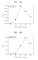
FIG. 10A is a graph showing chromaticity coordinate in CIE 1931 x, y chromaticity diagram relative to a viewing angle inOLED 30 shown inFIG. 3 ,FIG. 10B is a graph showing the chromaticity coordinate in CIE 1976 u', v' chromaticity diagram relative to the viewing angle with respect to coordinate values u' and v' inOLED 30 shown inFIG. 3 , andFIG. 10C is a graph showing a deviation (Del(u'v')) of a value u'v' relative to a viewing angle from the front view inOLED 30 shown inFIG. 3 . Referring toFIGS. 10A through 10C , it can be seen that even if the viewing angle increases, a color variation occurs within only a small range. On comparingFIG. 10C withFIG. 8C , it can be confirmed that a peak (about 0.017) in the deviation (Del(u'v')) of the value u' v' relative to the viewing angle inOLED 30 shown inFIG. 3 is about 10 times as low as a peak (about 0.116) in the deviation (Del(u'v')) of the value u'v' relative to a viewing angle inOLED 20 according to the comparative example. -
FIG. 11A is a graph showing chromaticity coordinate in CIE 1931 x, y chromaticity diagram relative to a viewing angle when white light is transmitted through an R color filter ofFIG. 5 inOLED 30 shown inFIG. 3 ,FIG. 11B is a graph showing chromaticity coordinate in CIE 1931 x, y chromaticity diagram relative to a viewing angle when white light is transmitted through a G color filter ofFIG. 5 inOLED 30 shown inFIG. 3 ,FIG. 11C is a graph showing chromaticity coordinate in CIE 1931 x, y chromaticity diagram relative to a viewing angle when white light is transmitted through a B color filter ofFIG. 5 inOLED 30 shown inFIG. 3 andFIG. 11D is a two dimensional graph showing chromaticity coordinate in CIE 1931 x, y chromaticity diagram relative to a viewing angle for white light when the white light is transmitted through all color filters ofFIG. 5 in the top-emitting white OLED shown inFIG. 3 .FIG. 12A is a graph showing the deviation of a value u' v' in CIE 1976 u', v' chromaticity diagram relative to a viewing angle when white light is transmitted through the R color filter ofFIG. 5 in the top-emitting white OLED shown inFIG. 3 ,FIG. 12B is a graph showing the deviation of a value u'v' in CIE 1976 u', v' chromaticity diagram relative to a viewing angle when white light is transmitted through the G color filter ofFIG. 5 inOLED 30 shown inFIG. 3 ,FIG. 12C is a graph showing the deviation of a value u'v' in CIE 1976 u', v' chromaticity diagram relative to a viewing angle when white light is transmitted through the B color filter ofFIG. 5 inOLED 30 shown inFIG. 3 , andFIG. 12D is a graph showing the deviation of a value u'v' in CIE 1976 u', v' chromaticity diagram relative to a viewing angle for white light when the white light is transmitted through all the color filters ofFIG. 5 in theOLED 30 shown inFIG. 3 . Referring toFIGS. 11A through 11D , it can be confirmed that after light is transmitted through the color filters, a color variation occurs within only a very small range. Also, referring toFIGS. 12A through 12D , it may be observed that after light is transmitted through the color filters, peaks in the deviation (Del(u'v')) for R, G, B, and white light are maintained very low. Specifically, the peaks in the deviation (Del(u'v')) for R, G, B, and white light are about 0.029, 0.04, 0.033, and 0.027, respectively. - When the above-described OLED according to the present invention is applied to a color display apparatus, the color display apparatus may greatly improve a color reproduction range and reduce a variation of color with a viewing angle.
-
FIG. 13 is a cross-sectional view of acolor display apparatus 100 using the white OLED ofFIG. 1 , according to an embodiment of the present invention. - Referring to
FIG. 13 ,respective electrodes 12 corresponding respectively to sub-pixels are disposed on a singlecommon substrate 11. A hole transport layer (HTL) 13, a first emission layer (EML) 14, anorganic layer 15, asecond EML 16, an electron injection layer (EIL) 17, atransmissive electrode 18, and an optical path controllayer 19 may be formed sequentially oncommon substrate 11 havingreflective electrodes 12. Atransparent front substrate 50 is disposed opposite optical path controllayer 19, and R, G, andB color filters front substrate 50. Although not shown inFIG. 13 , black matrix (BM) for completely absorbing external light may be further disposed between each pair of color filters in order to elevate visibility. Also, a low-refractive index layer (not shown), such as a gas layer or a low-refractive filler, may be further prepared betweenfront substrate 50 and optical path controllayer 19. Furthermore, a dielectric mirror or a thin metal mirror may be further provided on a top surface of optical path controllayer 19. - According to the present invention, as shown in
FIG. 13 , an OLED including electrodes and EMLs may be constructed such that all sub-pixels have the same structure irrespective of colors of the sub-pixels. Also, it is unnecessary to control an optical distance in a sub-pixel according to color, so that allreflective electrodes 12 disposed below the sub-pixels can have the same structure. In addition, since the OLED can emit almost pure white light, pure color can be created usingcolor filters - As explained thus far, the present embodiment provides a technique for improving the characteristics of the white OLED. However, the present invention is not limited to the white OLED and can be also applied to single-color OLEDs that are manufactured using an independent deposition process and permit respective pixels to emit light in different colors. For example, although
FIGS. 1 and3 illustrate at least two white EMLs, each white EML including R, B, and G EMLs, the present invention can be applied to a single-color OLED that includes only at least two single-color EMLs (i.e., at least two R EMLs, at least two B EMLs, or at least two G EMLs) instead of the white EMLs. In this case, a distance between at least two single-color EMLs that emit light in the same color satisfies the condition of constructive interference shown in Table 1. Also, single-color OLEDs that are deposited on R, G, and B sub-pixels to emit light in different colors are manufactured to the same thickness, and an optical path control layer prepared on a transmissive electrode is formed to a sufficiently great thickness, thereby causing multi-resonance. As a result, the single-color OLED that improves a color reproduction range and reduces a variation of color with a viewing angle can be embodied. A color display apparatus using the single-color OLEDs as R, G, and B sub-pixels may not employ thecolor filters FIG. 13 . - Although the top-emitting OLED was described above, the same principles can be also applied to a bottom-emitting OLED. Therefore, the present invention is not limited to the top-emitting OLED and can be applied likewise to the bottom-emitting OLED.
- While the present invention has been particularly shown and described with reference to exemplary embodiments thereof, it will be understood by one of ordinary skill in the art that various changes in form and details may be made therein without departing from the scope of the present invention as defined by the following claims.
Claims (15)
- An organic light emitting display (OLED), comprising:a reflective electrode and a transmissive or semi-transmissive electrode disposed opposite each other;at least two organic emission layers (EMLs) interposed between the reflective electrode and the transmissive or semi-transmissive electrode; andan optical path control layer disposed on an outer surface of the transmissive or semi-transmissive electrode,the OLED having a resonator formed between the reflective electrode and the optical path control layer and thus a resonance mode of light extracted from the optical path control layer being a multi-resonance mode having at least two modes in a visible light region, and a distance between the organic EMLs satisfying a condition of constructive interference between light beams emitted by the respective organic EMLs.
- The OLED of claim 1, in which the at least two organic EMLs are white EMLs, each white EML including a red (R) EML, a green (G) EML, and a blue (B) EML.
- The OLED of claim 2, in which the at least two organic EMLs are white EMLs, each white EML including two kinds of single000-color or multi-color EMLs that emit light in complementary colors.
- The OLED of claim 2 or 3, in which each of distances between the EMLs emitting light in a same color in the at least two organic EMLs satisfies the condition of the constructive interference.
- The OLED of claim 2, in which a distance between the EMLs emitting light in the same color in the at least two organic EMLs is greater than a distance that permits center wavelength of the color of the blue EML in order to satisfy the condition of the constructive interference.
- The OLED of claim 2, in which the distance between the EMLs emitting light in the same color of at least two organic EMLs has a toleration within ± 10% of a distance that permits center wavelength of the color of the blue EML to satisfy the condition of the constructive interference.
- The OLED of claim 1, in which the at least two organic EMLs are single-color EMLs that emit light in the same color.
- The OLED of any preceding claim, further comprising a PN junction layer interposed between the at least two organic EMLs, in which the PN junction layer includes an n-doped electron transport layer (ETL) and a p-doped hole transport layer (HTL).
- The OLED of any preceding claim, in which the optical path control layer is formed of a material having an optical transmittance of 90% or higher in a visible light region, and in which the optical path control layer has a refractive index in range of approximately from 1.6 to 2.6.
- The OLED of claim 9, in which the optical path control layer is formed of at least one selected from a group consisting of Al2O3, BaO, MgO, HfO2, ZrO2, CaO2, SrO2, Y2O3, Si3N4, AIN, GaN, ZnS, and CdS.
- The OLED of claim 9 or 10, in which the optical path control layer has a thickness in range of approximately from 300 nm to 900 nm.
- The OLED of any preceding claim, further comprising a multiple dielectric mirror layer disposed on a top surface of the optical path control layer, the multiple dielectric mirror layer formed by alternating a high-refractive index dielectric layer and a low-refractive index dielectric layer.
- The OLED of any preceding claim, further comprising a thin metal mirror layer disposed on the top surface of the optical path control layer.
- An OLED according to any preceding claim, further comprising:a transparent substrate disposed opposite the optical path control layer; anda plurality of color filters disposed on a surface of the transparent substrate,wherein the color display apparatus has resonators respectively formed between the reflective electrode and the optical path control layers so that a resonance mode of light extracted from the optical path control layer is a multi-resonance mode having at least two modes in a visible light region, and a distance between the organic EMLs satisfying the condition of constructive interference between light beams emitted by the respective organic EMLs.
- The apparatus of claim 14, in which the plurality of color filters are opposite to the optical path control layer.
Applications Claiming Priority (1)
| Application Number | Priority Date | Filing Date | Title |
|---|---|---|---|
| KR1020070104477A KR101434362B1 (en) | 2007-10-17 | 2007-10-17 | Organic light emitting device and color display apparatus employing the same |
Publications (2)
| Publication Number | Publication Date |
|---|---|
| EP2051312A2 true EP2051312A2 (en) | 2009-04-22 |
| EP2051312A3 EP2051312A3 (en) | 2011-05-25 |
Family
ID=40130622
Family Applications (1)
| Application Number | Title | Priority Date | Filing Date |
|---|---|---|---|
| EP08158039A Withdrawn EP2051312A3 (en) | 2007-10-17 | 2008-06-11 | Organic light emitting device and color display apparatus using the same |
Country Status (3)
| Country | Link |
|---|---|
| US (1) | US8587191B2 (en) |
| EP (1) | EP2051312A3 (en) |
| KR (1) | KR101434362B1 (en) |
Cited By (1)
| Publication number | Priority date | Publication date | Assignee | Title |
|---|---|---|---|---|
| US20100314636A1 (en) * | 2009-06-12 | 2010-12-16 | Sony Corporation | Organic light emitting device, display unit including the same, and illuminating device including the same |
Families Citing this family (19)
| Publication number | Priority date | Publication date | Assignee | Title |
|---|---|---|---|---|
| WO2011053279A1 (en) * | 2009-10-27 | 2011-05-05 | Hewlett-Packard Development Company, L.P. | Display for 3d holographic images |
| KR101108167B1 (en) | 2010-02-12 | 2012-02-06 | 삼성모바일디스플레이주식회사 | Organic light emitting display apparatus |
| JP5676949B2 (en) * | 2010-07-21 | 2015-02-25 | キヤノン株式会社 | Organic EL display device |
| KR20120119100A (en) | 2011-04-20 | 2012-10-30 | 삼성디스플레이 주식회사 | Organic light emitting device |
| KR101917752B1 (en) * | 2011-05-11 | 2018-11-13 | 가부시키가이샤 한도오따이 에네루기 켄큐쇼 | Light-emitting element, light-emitting module, light-emmiting panel, and light-emitting device |
| CN103531721B (en) * | 2013-11-05 | 2015-04-22 | 京东方科技集团股份有限公司 | Tandem organic light emitting diode device and display device |
| US9209422B2 (en) * | 2013-12-31 | 2015-12-08 | Lg Display Co., Ltd. | Organic light emitting display device with micro-cavity structure |
| KR102454348B1 (en) * | 2013-12-31 | 2022-10-17 | 엘지디스플레이 주식회사 | Organic Light Emitting Display Device having a micro cavity structure |
| KR102200343B1 (en) * | 2014-05-22 | 2021-01-07 | 엘지디스플레이 주식회사 | Organic light emitting diode display panel |
| KR102215147B1 (en) | 2014-08-14 | 2021-02-15 | 삼성디스플레이 주식회사 | Organic light emitting diode display |
| KR102231631B1 (en) | 2014-10-08 | 2021-03-24 | 삼성디스플레이 주식회사 | Organic light emitting diode display |
| KR102298757B1 (en) | 2014-10-24 | 2021-09-07 | 삼성디스플레이 주식회사 | Organic light emitting diode device |
| EP3016159B1 (en) | 2014-10-27 | 2021-12-08 | LG Display Co., Ltd. | White organic light emitting device |
| KR102505166B1 (en) * | 2015-07-30 | 2023-03-02 | 엘지디스플레이 주식회사 | Organic light emitting display device |
| JP6695977B2 (en) * | 2016-07-12 | 2020-05-20 | パイオニア株式会社 | Luminous system |
| US10529780B2 (en) * | 2017-02-28 | 2020-01-07 | Semiconductor Energy Laboratory Co., Ltd. | Display device, display module, and electronic device |
| JP6843727B2 (en) * | 2017-10-20 | 2021-03-17 | 株式会社Joled | Light emitting device |
| JP7176552B2 (en) * | 2020-08-31 | 2022-11-22 | セイコーエプソン株式会社 | electro-optical devices and electronics |
| CN114612437B (en) * | 2022-03-15 | 2024-04-09 | 深圳市科泰兴业科技有限公司 | AMOLED-based display image quality improvement method |
Citations (2)
| Publication number | Priority date | Publication date | Assignee | Title |
|---|---|---|---|---|
| EP1401034A2 (en) | 2002-09-18 | 2004-03-24 | Samsung NEC Mobile Display Co. Ltd. | Organic electroluminescent device using optical resonance effect |
| EP1478025A2 (en) | 2003-05-13 | 2004-11-17 | EASTMAN KODAK COMPANY (a New Jersey corporation) | Cascaded organic electroluminescent device having connecting units with n-type and p-type organic layers |
Family Cites Families (12)
| Publication number | Priority date | Publication date | Assignee | Title |
|---|---|---|---|---|
| US5478658A (en) * | 1994-05-20 | 1995-12-26 | At&T Corp. | Article comprising a microcavity light source |
| US6133692A (en) * | 1998-06-08 | 2000-10-17 | Motorola, Inc. | White light generating organic electroluminescent device and method of fabrication |
| US6680570B2 (en) | 2001-03-21 | 2004-01-20 | Agilent Technologies, Inc. | Polymer organic light emitting device with improved color control |
| JP2004127588A (en) * | 2002-09-30 | 2004-04-22 | Toyota Industries Corp | Light-emitting device, display, and luminaire |
| US7138763B2 (en) * | 2003-11-14 | 2006-11-21 | Eastman Kodak Company | Organic electroluminescent devices having a stability-enhancing layer |
| CN1954645A (en) * | 2004-05-18 | 2007-04-25 | 出光兴产株式会社 | Blue organic electroluminescent element and display device |
| JP4693593B2 (en) * | 2004-11-16 | 2011-06-01 | 京セラ株式会社 | Light emitting device |
| US8569948B2 (en) * | 2004-12-28 | 2013-10-29 | Samsung Display Co., Ltd. | Electroluminescent devices and methods of making electroluminescent devices including an optical spacer |
| US7642205B2 (en) * | 2005-04-08 | 2010-01-05 | Mattson Technology, Inc. | Rapid thermal processing using energy transfer layers |
| TW200714131A (en) * | 2005-07-29 | 2007-04-01 | Sanyo Electric Co | Organic electroluminescent element and organic electroluminescent display device |
| US7583712B2 (en) * | 2006-06-16 | 2009-09-01 | Pbc Lasers Gmbh | Optoelectronic device and method of making same |
| US7816859B2 (en) * | 2007-04-30 | 2010-10-19 | Global Oled Technology Llc | White light tandem OLED |
-
2007
- 2007-10-17 KR KR1020070104477A patent/KR101434362B1/en active IP Right Grant
-
2008
- 2008-05-21 US US12/153,608 patent/US8587191B2/en active Active
- 2008-06-11 EP EP08158039A patent/EP2051312A3/en not_active Withdrawn
Patent Citations (2)
| Publication number | Priority date | Publication date | Assignee | Title |
|---|---|---|---|---|
| EP1401034A2 (en) | 2002-09-18 | 2004-03-24 | Samsung NEC Mobile Display Co. Ltd. | Organic electroluminescent device using optical resonance effect |
| EP1478025A2 (en) | 2003-05-13 | 2004-11-17 | EASTMAN KODAK COMPANY (a New Jersey corporation) | Cascaded organic electroluminescent device having connecting units with n-type and p-type organic layers |
Cited By (2)
| Publication number | Priority date | Publication date | Assignee | Title |
|---|---|---|---|---|
| US20100314636A1 (en) * | 2009-06-12 | 2010-12-16 | Sony Corporation | Organic light emitting device, display unit including the same, and illuminating device including the same |
| US8405098B2 (en) * | 2009-06-12 | 2013-03-26 | Sony Corporation | Organic light emitting device, display unit including the same, and illuminating device including the same |
Also Published As
| Publication number | Publication date |
|---|---|
| KR101434362B1 (en) | 2014-08-26 |
| KR20090039065A (en) | 2009-04-22 |
| US20090102362A1 (en) | 2009-04-23 |
| EP2051312A3 (en) | 2011-05-25 |
| US8587191B2 (en) | 2013-11-19 |
Similar Documents
| Publication | Publication Date | Title |
|---|---|---|
| EP2051312A2 (en) | Organic light emitting device and color display apparatus using the same | |
| US8102118B2 (en) | White organic light emitting device and color display apparatus employing the same | |
| US8227978B2 (en) | White organic light emitting device and color display apparatus employing the same | |
| US7893612B2 (en) | LED device having improved light output | |
| US9570517B2 (en) | Organic light emitting display device and method of manufacturing the same | |
| US7750564B2 (en) | High efficiency organic light emitting device | |
| US7098590B2 (en) | Organic electroluminescent device using optical resonance effect | |
| US7741770B2 (en) | LED device having improved light output | |
| EP2562816B1 (en) | Organic light emitting diode display and manufacturing method thereof | |
| JP4507718B2 (en) | Color organic EL display and manufacturing method thereof | |
| KR101528242B1 (en) | White organic light emitting device and color display apparatus employing the same | |
| US20090051283A1 (en) | Led device having improved contrast | |
| KR20100080801A (en) | Led device having improved light output | |
| US20090142983A1 (en) | Flat panel display and method of manufacturing the same | |
| US9343510B2 (en) | Organic light emitting display device | |
| CN108123048B (en) | Light emitting device, display device, and lighting device | |
| KR100490535B1 (en) | Organic electroluminescence device | |
| US8022612B2 (en) | White-light LED having two or more commonly controlled portions with improved angular color performance | |
| KR20070058765A (en) | Light emitting diode | |
| KR20140104248A (en) | Organic Light Emitting Display Device | |
| JP2023530043A (en) | Multimodal microcavity OLED with multiple blue emitting layers | |
| CN109638037B (en) | Full-color display module and manufacturing method thereof |
Legal Events
| Date | Code | Title | Description |
|---|---|---|---|
| PUAI | Public reference made under article 153(3) epc to a published international application that has entered the european phase |
Free format text: ORIGINAL CODE: 0009012 |
|
| AK | Designated contracting states |
Kind code of ref document: A2 Designated state(s): AT BE BG CH CY CZ DE DK EE ES FI FR GB GR HR HU IE IS IT LI LT LU LV MC MT NL NO PL PT RO SE SI SK TR |
|
| AX | Request for extension of the european patent |
Extension state: AL BA MK RS |
|
| RAP1 | Party data changed (applicant data changed or rights of an application transferred) |
Owner name: SAMSUNG ELECTRONICS CO., LTD. Owner name: SAMSUNG SDI CO., LTD. |
|
| RAP1 | Party data changed (applicant data changed or rights of an application transferred) |
Owner name: SAMSUNG ELECTRONICS CO., LTD. Owner name: SAMSUNG MOBILE DISPLAY CO., LTD. |
|
| PUAL | Search report despatched |
Free format text: ORIGINAL CODE: 0009013 |
|
| AK | Designated contracting states |
Kind code of ref document: A3 Designated state(s): AT BE BG CH CY CZ DE DK EE ES FI FR GB GR HR HU IE IS IT LI LT LU LV MC MT NL NO PL PT RO SE SI SK TR |
|
| AX | Request for extension of the european patent |
Extension state: AL BA MK RS |
|
| 17P | Request for examination filed |
Effective date: 20111116 |
|
| AKX | Designation fees paid |
Designated state(s): GB NL |
|
| REG | Reference to a national code |
Ref country code: DE Ref legal event code: R108 |
|
| REG | Reference to a national code |
Ref country code: DE Ref legal event code: R108 Effective date: 20120201 |
|
| RAP1 | Party data changed (applicant data changed or rights of an application transferred) |
Owner name: SAMSUNG MOBILE DISPLAY CO., LTD. Owner name: SAMSUNG ELECTRONICS CO., LTD. |
|
| RAP1 | Party data changed (applicant data changed or rights of an application transferred) |
Owner name: SAMSUNG DISPLAY CO., LTD. Owner name: SAMSUNG ELECTRONICS CO., LTD. |
|
| RAP1 | Party data changed (applicant data changed or rights of an application transferred) |
Owner name: SAMSUNG DISPLAY CO., LTD. |
|
| 17Q | First examination report despatched |
Effective date: 20141212 |
|
| RAP1 | Party data changed (applicant data changed or rights of an application transferred) |
Owner name: SAMSUNG DISPLAY CO., LTD. |
|
| STAA | Information on the status of an ep patent application or granted ep patent |
Free format text: STATUS: THE APPLICATION IS DEEMED TO BE WITHDRAWN |
|
| 18D | Application deemed to be withdrawn |
Effective date: 20181019 |