EP2051303B1 - Method to detect poor infrared rays, Microchip that is able to detect poor infrared rays and apparatus working with these microchips - Google Patents
Method to detect poor infrared rays, Microchip that is able to detect poor infrared rays and apparatus working with these microchips Download PDFInfo
- Publication number
- EP2051303B1 EP2051303B1 EP08013302.8A EP08013302A EP2051303B1 EP 2051303 B1 EP2051303 B1 EP 2051303B1 EP 08013302 A EP08013302 A EP 08013302A EP 2051303 B1 EP2051303 B1 EP 2051303B1
- Authority
- EP
- European Patent Office
- Prior art keywords
- semiconductors
- telluride
- microchip
- blind holes
- zinc
- Prior art date
- Legal status (The legal status is an assumption and is not a legal conclusion. Google has not performed a legal analysis and makes no representation as to the accuracy of the status listed.)
- Active
Links
Images
Classifications
-
- G—PHYSICS
- G01—MEASURING; TESTING
- G01J—MEASUREMENT OF INTENSITY, VELOCITY, SPECTRAL CONTENT, POLARISATION, PHASE OR PULSE CHARACTERISTICS OF INFRARED, VISIBLE OR ULTRAVIOLET LIGHT; COLORIMETRY; RADIATION PYROMETRY
- G01J1/00—Photometry, e.g. photographic exposure meter
- G01J1/42—Photometry, e.g. photographic exposure meter using electric radiation detectors
- G01J1/44—Electric circuits
-
- G—PHYSICS
- G01—MEASURING; TESTING
- G01J—MEASUREMENT OF INTENSITY, VELOCITY, SPECTRAL CONTENT, POLARISATION, PHASE OR PULSE CHARACTERISTICS OF INFRARED, VISIBLE OR ULTRAVIOLET LIGHT; COLORIMETRY; RADIATION PYROMETRY
- G01J5/00—Radiation pyrometry, e.g. infrared or optical thermometry
- G01J5/02—Constructional details
- G01J5/08—Optical arrangements
- G01J5/0853—Optical arrangements having infrared absorbers other than the usual absorber layers deposited on infrared detectors like bolometers, wherein the heat propagation between the absorber and the detecting element occurs within a solid
-
- H—ELECTRICITY
- H10—SEMICONDUCTOR DEVICES; ELECTRIC SOLID-STATE DEVICES NOT OTHERWISE PROVIDED FOR
- H10F—INORGANIC SEMICONDUCTOR DEVICES SENSITIVE TO INFRARED RADIATION, LIGHT, ELECTROMAGNETIC RADIATION OF SHORTER WAVELENGTH OR CORPUSCULAR RADIATION
- H10F77/00—Constructional details of devices covered by this subclass
- H10F77/50—Encapsulations or containers
-
- H—ELECTRICITY
- H10—SEMICONDUCTOR DEVICES; ELECTRIC SOLID-STATE DEVICES NOT OTHERWISE PROVIDED FOR
- H10W—GENERIC PACKAGES, INTERCONNECTIONS, CONNECTORS OR OTHER CONSTRUCTIONAL DETAILS OF DEVICES COVERED BY CLASS H10
- H10W40/00—Arrangements for thermal protection or thermal control
- H10W40/10—Arrangements for heating
Definitions
- the invention relates to a method for the detection of poor rays of infrared wavelength, to a microchip that is able to detect poor infrared rays and to an apparatus working with these microchips.
- a closed body of a working machine or an electronic apparatus or a human or an animal body is to detect a source of little higher temperature than normal, when defects beginn to happen.
- an electronic apparatus more warmth as usual can appear when a resistance is stressed by a to high voltage, in a working machine is in the case of a lack of oil more warmth on a place produced which breaks at first, in a human or animal body arises the temperature where the body has to defend themselves against a growing cancer.
- This invention gives a possibility to detect and to locate little growings cancers and others hidden places of parts of a machine with increased temperature.
- the invention does do it with a special microchip which is able to change photons in electrons.
- US5561295 discloses such a detector in which a continuous film of light detecting material is covered with a contact grid.
- This microchip of the invention consists of a plate of glas or an other insulating material with a rough surface on the one side.
- the front surface of this plate is rough by a plurality of blind holes, the ground of each of theese blind holes is covered with a thin layer of metal, in each of the blind holes are located little semiconducting crystals of a kind of material that emitts one or more electrons by each hit of an infrared light beam, the surface of this plate and the blind holes are covered with a net of very thin wires and the active part of this net of very thin wires has on its ends rails of metal to collect and transmit the electrons to a measuring instrument.
- the blind holes can have the form of hemispheres, of cylindrical holes or honeycombs.
- Each blind hole has an inner surface of a thin layer of metal to deduct electrons from the surface or the edges of the cristals situated in the blind holes. From these metal layers and from the free edges of the cristalls the thin wires covering the surface of the glasplate deduct the electrons to the rails and to the measuring instrument (to measure voltage differences).
- the cristals put in the blind holes are semiconductors made from atoms of the group VI elements such as ⁇ Cadmium selenide Cd Se ⁇ Cadmium sulfide Cd Ss ⁇ Cadmium telluride Cd Te ⁇ Zinc oxide Zn O ⁇ Zinc selenide Zn Se ⁇ Zinc sulfide Zn S ⁇ Zinc telluride Zn Te and/or from II-VI ternary alloy semiconductos ⁇ Cadmium zinc telluride Cd Zn Te ⁇ Mercury cadmium telluride Hg Cd Te ⁇ Mercury zink telluride Hg Zn Te ⁇ Mercury zink selenide Hg Zn Se and/or from a I-VII semiconductor ⁇ Cuprous chloride Cu Cl and/or from IV - IV semiconductors ⁇ Lead selenide Pb Se ⁇ Lead sulfide Pb S ⁇ Lead telluride Pb Te ⁇ Tin sulfide Sn S ⁇ Tin telluride Sn Te and/or from
- This polymer should be a good conductor of electrons like dendrimers and nanocarbon tube, especially ⁇ Poly-acethylene ⁇ Fullerenes ⁇ Melamine Poly-amidoamine ⁇ non-polar polymers ⁇ Fluoropolymers ⁇ Fluorocarbons ⁇ Polytetrafluoroethylene.
- This invention relates also to a microchip that is able to detect poor infrared rays.
- This microchip consists of a thin plate of glas, silicon or another hard electrical insulating material, the front surface of this glas plate is rough by a plurality of blind holes, the ground of the blind holes is covered with a thin layer of metal, in the blind holes are situated little crystals of a kind of material that that is an infrared absorber and emitts one or more electrons by each hit of an infrared light beam, the surface of this plate of glas and the blind holes is covered with a net of very thin wires and the active part of this net of very thin wires has on its ends rails to collect the electrons.
- This microchip is able to detect poor infrared reys and to change whose energy in electrons. That makes it possible to find out the presence and the power of a infrared radiation also in the case that this radiation is poor.
- the microchip of the invention can have a front surface of grooves in form of a regular shape like little honeycombs.
- crystals of this microchip located in the blind holes are surrounded by a polymer with electrical conductivity and/or some metal coating.
- the semiconductors or the theese semiconductor carrying glas plate can be attached to or embedded in a heat deducting material.
- Theese microchips can be part of an apparatus for the detection of a source of poor infrared rays in a body consisting of one or more microchips und a device for the comparison the output of electrons of the microchip(s) on diverse locations of the surface of the body, par example in an apparatus with one microchip to measure the ground-radiation of the body and another microchip to measure the soft increased radiation of a defect.
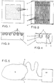
- the microchip consists of a glas plate 1 with a rough surface on its front side, because there are many blind holes 2.
- blind holes 2 are embedded cristals 3 of semiconductos surrounded by an acid polymer solution.
- the ground and the walls of the blind holes 2 are covered with a thin layer 4 of metal.
- Over the whole glas plate 1 with the cristals is laid a web of thin wires leading the electrons in the cristals produced electrons to the rails 5 acting as electrodes.
- the apparatus 6 works with two microchips 7,8 on a body 9 to investigate.
- Microchip 7 is fastend on the body to ascertain the ground-radiation
- microchip 8 is movable to find out a location with encreased radiation.
Landscapes
- Physics & Mathematics (AREA)
- General Physics & Mathematics (AREA)
- Spectroscopy & Molecular Physics (AREA)
- Light Receiving Elements (AREA)
- Photometry And Measurement Of Optical Pulse Characteristics (AREA)
- Radiation Pyrometers (AREA)
Description
- The invention relates to a method for the detection of poor rays of infrared wavelength, to a microchip that is able to detect poor infrared rays and to an apparatus working with these microchips.
- In a closed body of a working machine or an electronic apparatus or a human or an animal body is to detect a source of little higher temperature than normal, when defects beginn to happen. In an electronic apparatus more warmth as usual can appear when a resistance is stressed by a to high voltage, in a working machine is in the case of a lack of oil more warmth on a place produced which breaks at first, in a human or animal body arises the temperature where the body has to defend themselves against a growing cancer.
- In all these cases the beginning of a growing defect can be located when it is possible to measure only a little higher temperature in a wide distance and to locate the place of this higher temperature.
- This invention gives a possibility to detect and to locate little growings cancers and others hidden places of parts of a machine with increased temperature. The invention does do it with a special microchip which is able to change photons in electrons.
US5561295 discloses such a detector in which a continuous film of light detecting material is covered with a contact grid. This microchip of the invention consists of a plate of glas or an other insulating material with a rough surface on the one side. The front surface of this plate is rough by a plurality of blind holes, the ground of each of theese blind holes is covered with a thin layer of metal, in each of the blind holes are located little semiconducting crystals of a kind of material that emitts one or more electrons by each hit of an infrared light beam, the surface of this plate and the blind holes are covered with a net of very thin wires and the active part of this net of very thin wires has on its ends rails of metal to collect and transmit the electrons to a measuring instrument. - The blind holes can have the form of hemispheres, of cylindrical holes or honeycombs. Each blind hole has an inner surface of a thin layer of metal to deduct electrons from the surface or the edges of the cristals situated in the blind holes. From these metal layers and from the free edges of the cristalls the thin wires covering the surface of the glasplate deduct the electrons to the rails and to the measuring instrument (to measure voltage differences).
- The cristals put in the blind holes are semiconductors made from atoms of the group VI elements such as
< Cadmium selenide Cd Se < Cadmium sulfide Cd Ss < Cadmium telluride Cd Te < Zinc oxide Zn O < Zinc selenide Zn Se < Zinc sulfide Zn S < Zinc telluride Zn Te < Cadmium zinc telluride Cd Zn Te < Mercury cadmium telluride Hg Cd Te < Mercury zink telluride Hg Zn Te < Mercury zink selenide Hg Zn Se < Cuprous chloride Cu Cl < Lead selenide Pb Se < Lead sulfide Pb S < Lead telluride Pb Te < Tin sulfide Sn S < Tin telluride Sn Te < Lead tin telluride Pb Sn Te < Thallium tin telluride Tl Sn Te < Thallium germanium telluride TI Ge Te < Bismuth telluride Bi Te < II - V semiconductors < Cadmium phosphide Cd P < Cadmium phosphide Cd P < Cadmium arsenide Cd As < Cadmium antimonide Cd Sb < Zinc phosphide Zn P < Zinc arsenide Zn As < Zinc antimonide Zn Sb - For this method it is usefull if the cristals of the semiconductors are sourrounded by a polymer which is grown in an acid fluid.
- This polymer should be a good conductor of electrons like dendrimers and nanocarbon tube,
especially< Poly-acethylene < Fullerenes < Melamine Poly-amidoamine < non-polar polymers < Fluoropolymers < Fluorocarbons < Polytetrafluoroethylene. - This invention relates also to a microchip that is able to detect poor infrared rays. This microchip consists of a thin plate of glas, silicon or another hard electrical insulating material, the front surface of this glas plate is rough by a plurality of blind holes, the ground of the blind holes is covered with a thin layer of metal, in the blind holes are situated little crystals of a kind of material that that is an infrared absorber and emitts one or more electrons by each hit of an infrared light beam, the surface of this plate of glas and the blind holes is covered with a net of very thin wires and the active part of this net of very thin wires has on its ends rails to collect the electrons.
- This microchip is able to detect poor infrared reys and to change whose energy in electrons. That makes it possible to find out the presence and the power of a infrared radiation also in the case that this radiation is poor.
- The microchip of the invention can have a front surface of grooves in form of a regular shape like little honeycombs.
- It is advantageous if the crystals of this microchip located in the blind holes are surrounded by a polymer with electrical conductivity and/or some metal coating.
- Because heat can be generated in the microchip of this invention the semiconductors or the theese semiconductor carrying glas plate can be attached to or embedded in a heat deducting material.
- It is advantageous for the construction of this microchip if the net of thin wires over the semiconductor cristals is so situated that they let through infrared light and catch the most of the in the semiconductors produced electrons.
- To hinder a demolation of the microchip by sweat of a human body or oil of a machine or other influences it is advantageous to have a protection layer over the web of thin wires against a direct connection of the thin wires with the investigated body.
- Theese microchips can be part of an apparatus for the detection of a source of poor infrared rays in a body consisting of one or more microchips und a device for the comparison the output of electrons of the microchip(s) on diverse locations of the surface of the body, par example in an apparatus with one microchip to measure the ground-radiation of the body and another microchip to measure the soft increased radiation of a defect.
- The enclosed drawing shows in
- Fig.1
- a view of the surface of the microchip.
- Fig.2
- a crossection through the microchip.
- Fig.3
- an enlarged part of the crossection.
- Fig.4
- a wiring diagramm of the apparatus using the microchips.
- The microchip consists of a
glas plate 1 with a rough surface on its front side, because there are manyblind holes 2. In theeseblind holes 2 are embedded cristals 3 of semiconductos surrounded by an acid polymer solution. The ground and the walls of theblind holes 2 are covered with athin layer 4 of metal. Over thewhole glas plate 1 with the cristals is laid a web of thin wires leading the electrons in the cristals produced electrons to therails 5 acting as electrodes. - The
apparatus 6 works with twomicrochips body 9 to investigate. Microchip 7 is fastend on the body to ascertain the ground-radiation,microchip 8 is movable to find out a location with encreased radiation.
Claims (11)
- Method for producing a microchip that is able to detect poor rays of infrared wavelength by taking a thin plate of glass (1) or another hard electrical insulating material, the front surface is rough by a plurality of blind holes, (2) by covering the blind holes with a thin layer of metal, (4) by bringing in in the holes little crystals (3) of a kind of material that emits one or more electrons by each hit of an infrared light beam, by covering the surface of the plate and the blind holes with a net of very thin wires (5) and by collecting the electrons in rails (6) at the ends of the active part of the net of very thin wires and with semiconductors as crystals of a kind of material that emits one or more electrons by each hit of an infrared light beam.
- Method for producing a microchip according claim 1 using crystals in the blind holes as
< Cadmium selenide Cd Se < Cadmium sulfide Cd S < Cadmium telluride Cd Te < Zinc oxide Zn O < Zinc selenide Zn Se < Zinc sulfide Zn S < Zinc telluride Zn Te < Cadmium zinc telluride Cd Zn Te < Mercury cadmium telluride Hg Cd Te < Mercury zinc telluride Hg Zn Te < Mercury zinc selenide Hg Zn Se < Cuprous chloride Cu Cl < Lead selenide Pb Se < Lead sulfide Pb S < Lead telluride Pb Te < Tin sulfide Sn S < Tin telluride Sn Te < Lead tin telluride Pb Sn Te < Thallium tin telluride TI Sn Te < Thallium germanium telluride Tl Ge Te < Bismuth telluride Bi Te < II - V semiconductors < Cadmium phosphide Cd P < Cadmium phosphide Cd P < Cadmium arsenide Cd As < Cadmium antimonide Cd Sb < Zinc phosphide Zn P < Zinc arsenide Zn As < Zinc antimonide Zn Sb - Method according claims 1 and 2 with semiconductors surrounded by a polymer which is grown in a acid fluid.
- Method according claim 1 to 3 using a polymer which should be a good conductor of electrons like dendrimers and nanocarbon tube, especially
< Poly-acetylene < Fullerenes < Melamine < Poly-amidoamine < non-polar polymers < Fluoropolymers < Fluorocarbons < Polytetrafluoroethylene. - Microchip
that is able to detect poor infrared rays consisting of a thin plate of glass (1) or another hard electrical insulating material, the front surface of this glass plate is rough by a plurality of blind holes, (2) the ground of the blind holes is covered with a thin layer of metal, (4) in the blind holes are situated little semiconductors crystals (3) of a kind of material that that is an infrared absorber and emits one or more electrons by each hit of an infrared light beam, the surface of this plate of glass and the blind holes is covered with a net of very thin wires (5) and the active part of this net of very thin wires has on its ends rails (6) to collect the electrons. - Microchip according claim 5
with a front surface of grooves in form of a regular shape like little honeycombs. - Microchip according claim 5
with crystals situated in the blind holes surrounded by a polymer with electrical conductivity. - Microchip according claim 5
whose semiconductors or glass plate are attached to or embedded in a heat deducted material. - Microchip according claim 7
with a net of thin wires over the semiconductor crystals so situated that they let through infrared light and catch the most of the in the semiconductors produced electrons. - Microchip according claim 5
with a protection layer over the web of thin wires against a direct connection of the thin wires with a investigated body. - Apparatus for the detection of a source of poor rays of infrared wavelength in a body consisting of one or more microchips according claim 5 and device for the comparison the output of electrons of the microchip(s) on diverse locations of the surface of the body.
Applications Claiming Priority (1)
| Application Number | Priority Date | Filing Date | Title |
|---|---|---|---|
| US11/895,800 US20090001491A1 (en) | 2006-10-30 | 2007-08-28 | Method for producing a microchip that is able to detect infrared light with a semiconductor at room temperature |
Publications (3)
| Publication Number | Publication Date |
|---|---|
| EP2051303A2 EP2051303A2 (en) | 2009-04-22 |
| EP2051303A3 EP2051303A3 (en) | 2014-12-17 |
| EP2051303B1 true EP2051303B1 (en) | 2017-07-05 |
Family
ID=40418957
Family Applications (1)
| Application Number | Title | Priority Date | Filing Date |
|---|---|---|---|
| EP08013302.8A Active EP2051303B1 (en) | 2007-08-28 | 2008-07-24 | Method to detect poor infrared rays, Microchip that is able to detect poor infrared rays and apparatus working with these microchips |
Country Status (2)
| Country | Link |
|---|---|
| US (1) | US20090001491A1 (en) |
| EP (1) | EP2051303B1 (en) |
Cited By (1)
| Publication number | Priority date | Publication date | Assignee | Title |
|---|---|---|---|---|
| EP4336855A1 (en) | 2022-09-07 | 2024-03-13 | Biomimetics Technologies Inc. | Detector, device and method for imaging ir and/or microwave irradiation |
Families Citing this family (3)
| Publication number | Priority date | Publication date | Assignee | Title |
|---|---|---|---|---|
| CN102465327B (en) * | 2010-11-16 | 2016-01-06 | 富士康(昆山)电脑接插件有限公司 | Forming method of nanotube upright cluster |
| US10217891B2 (en) | 2013-05-09 | 2019-02-26 | Universitat De Valencia | Method for producing biomimetic-inspired infrared sensors from zinc phosphide microwires |
| CN108365021A (en) * | 2018-02-06 | 2018-08-03 | 无锡元创华芯微机电有限公司 | A kind of infrared detector wafer packaging method |
Family Cites Families (15)
| Publication number | Priority date | Publication date | Assignee | Title |
|---|---|---|---|---|
| GB1568958A (en) * | 1976-10-22 | 1980-06-11 | Mullard Ltd | Methods of manufacturing infra-red sensitive devices |
| US5880510A (en) * | 1988-05-11 | 1999-03-09 | Raytheon Company | Graded layer passivation of group II-VI infrared photodetectors |
| US5077092A (en) * | 1989-06-30 | 1991-12-31 | Texas Instruments Incorporated | Method and apparatus for deposition of zinc sulfide films |
| US5198267A (en) * | 1991-09-20 | 1993-03-30 | Allied-Signal Inc. | Fluoropolymer blend anti-reflection coatings and coated articles |
| US5561295A (en) * | 1994-07-29 | 1996-10-01 | Litton Systems, Inc. | Infrared-responsive photoconductive array and method of making |
| JP2773730B2 (en) * | 1996-03-07 | 1998-07-09 | 日本電気株式会社 | Photoconductive infrared detector |
| US6730212B1 (en) * | 2000-10-03 | 2004-05-04 | Hrl Laboratories, Llc | Sensor for chemical and biological materials |
| US6890834B2 (en) * | 2001-06-11 | 2005-05-10 | Matsushita Electric Industrial Co., Ltd. | Electronic device and method for manufacturing the same |
| GB0121444D0 (en) * | 2001-09-05 | 2001-10-24 | Univ Strathclyde | Sensor |
| DE10221857A1 (en) * | 2002-05-16 | 2003-11-27 | Osram Opto Semiconductors Gmbh | Process for applying a semiconductor chip on a thermal and/or electrically conducting connecting part arranged in or on a plastic housing body comprises using a soft soldering process |
| US7135357B2 (en) * | 2003-10-06 | 2006-11-14 | E. I. Du Pont De Nemours And Company | Process for making an organic electronic device having a roughened surface heat sink |
| US20050211991A1 (en) * | 2004-03-26 | 2005-09-29 | Kyocera Corporation | Light-emitting apparatus and illuminating apparatus |
| US7985424B2 (en) * | 2004-04-20 | 2011-07-26 | Dendritic Nanotechnologies Inc. | Dendritic polymers with enhanced amplification and interior functionality |
| US20070213617A1 (en) * | 2006-02-16 | 2007-09-13 | Berman Herbert L | Infrared detection of cancerous tumors and other subsurface anomalies in the human breast and in other body parts |
| US20070299162A1 (en) * | 2006-06-27 | 2007-12-27 | Gelcore Llc | Optoelectronic device |
-
2007
- 2007-08-28 US US11/895,800 patent/US20090001491A1/en not_active Abandoned
-
2008
- 2008-07-24 EP EP08013302.8A patent/EP2051303B1/en active Active
Non-Patent Citations (1)
| Title |
|---|
| None * |
Cited By (1)
| Publication number | Priority date | Publication date | Assignee | Title |
|---|---|---|---|---|
| EP4336855A1 (en) | 2022-09-07 | 2024-03-13 | Biomimetics Technologies Inc. | Detector, device and method for imaging ir and/or microwave irradiation |
Also Published As
| Publication number | Publication date |
|---|---|
| EP2051303A3 (en) | 2014-12-17 |
| EP2051303A2 (en) | 2009-04-22 |
| US20090001491A1 (en) | 2009-01-01 |
Similar Documents
| Publication | Publication Date | Title |
|---|---|---|
| US11784278B2 (en) | Photovoltaic devices and method of making | |
| Yang et al. | Transparent flexible thermoelectric material based on non-toxic earth-abundant p-type copper iodide thin film | |
| Park et al. | High power output based on watch-strap-shaped body heat harvester using bulk thermoelectric materials | |
| Veale et al. | Chromium compensated gallium arsenide detectors for X-ray and γ-ray spectroscopic imaging | |
| ES2546311T3 (en) | Improved assembly of photovoltaic cells | |
| Fridjine et al. | A new parameter: an abacus for optimizing pv–t hybrid solar device functional materials using the Boubaker polynomials expansion scheme | |
| US7179986B2 (en) | Self-assembled quantum dot superlattice thermoelectric materials and devices | |
| EP2051303A2 (en) | Method to detect poor infrared rays, Microchip that is able to detect poor infrared rays and apparatus working with these microchips | |
| RU2722062C2 (en) | Radiation detector and image forming device | |
| Kim et al. | Modeling of a honeycomb-shaped pyroelectric energy harvester for human body heat harvesting | |
| JPWO2020049398A1 (en) | Imaging equipment and electronic equipment | |
| Kiruthika et al. | Large area transparent ZnO photodetectors with Au wire network electrodes | |
| JP2024015126A (en) | semiconductor equipment | |
| Mohammed et al. | Investigating the optical and electrical characteristics of As60Cu40-xSex thin films prepared using pulsed laser deposition method | |
| ES2965453T3 (en) | Electromagnetic radiation detector | |
| Lee et al. | Transparent metal-oxide personal UV monitoring device with machine learning advancement | |
| Sweet et al. | Scalable solar thermoelectrics and photovoltaics (SUNTRAP) | |
| Odobescu et al. | Electron correlation effects in transport and tunneling spectroscopy of the Si (111)-7× 7 surface | |
| Kim et al. | Realization of high‐performance screen‐printed flexible thermoelectric generator by improving contact characteristics | |
| Gedda et al. | Metal Halide Perovskites for High-Energy Radiation Detection | |
| Zong et al. | Flexible thermoelectric film sensor for optical power detection and multi-modal sensing | |
| Tamasi et al. | A theoretical approach to photosynthetically active radiation silicon sensor | |
| Adnani et al. | A position-sensitive microstrip detector using amorphous selenium photoconductor | |
| Maiorova et al. | Photoconductivity of pyrolytic CdS films alloyed with Cs | |
| Henry et al. | The role of the schottky metal in optical responses of optical position sensitive detector |
Legal Events
| Date | Code | Title | Description |
|---|---|---|---|
| PUAI | Public reference made under article 153(3) epc to a published international application that has entered the european phase |
Free format text: ORIGINAL CODE: 0009012 |
|
| AK | Designated contracting states |
Kind code of ref document: A2 Designated state(s): AT BE BG CH CY CZ DE DK EE ES FI FR GB GR HR HU IE IS IT LI LT LU LV MC MT NL NO PL PT RO SE SI SK TR |
|
| AX | Request for extension of the european patent |
Extension state: AL BA MK RS |
|
| RIN1 | Information on inventor provided before grant (corrected) |
Inventor name: VON SCHROEDER, HERBERT P Inventor name: RIZVI, SYED W. H. Inventor name: ISRAELOWITZ, MEIR Inventor name: HOLMES, CHRIS Inventor name: GILLE, CHRISTOPH |
|
| RIN1 | Information on inventor provided before grant (corrected) |
Inventor name: P.VON SCHROEDER, HERBERT Inventor name: RIZVI, SYED W. H. Inventor name: ISRAELOWITZ, MEIR Inventor name: HOLMES, CHRIS Inventor name: GILLE, CHRISTOPH |
|
| RIN1 | Information on inventor provided before grant (corrected) |
Inventor name: P.VON SCHROEDER, HERBERT Inventor name: RIZVI, SYED W. H. Inventor name: ISRAELOWITZ, MEIR Inventor name: HOLM, CHRIS Inventor name: GILLE, CHRISTOPH |
|
| RIN1 | Information on inventor provided before grant (corrected) |
Inventor name: P.VON SCHROEDER, HERBERT Inventor name: RIZVI, SYED W. H. Inventor name: ISRAELOWITZ, MEIR Inventor name: HOLMES, CHRIS Inventor name: GILLE, CHRISTOPH |
|
| PUAL | Search report despatched |
Free format text: ORIGINAL CODE: 0009013 |
|
| RIC1 | Information provided on ipc code assigned before grant |
Ipc: H01L 31/0352 20060101ALI20141104BHEP Ipc: H01L 31/0203 20140101AFI20141104BHEP Ipc: A61B 5/00 20060101ALI20141104BHEP |
|
| AK | Designated contracting states |
Kind code of ref document: A3 Designated state(s): AT BE BG CH CY CZ DE DK EE ES FI FR GB GR HR HU IE IS IT LI LT LU LV MC MT NL NO PL PT RO SE SI SK TR |
|
| AX | Request for extension of the european patent |
Extension state: AL BA MK RS |
|
| 17P | Request for examination filed |
Effective date: 20150512 |
|
| AKX | Designation fees paid |
Designated state(s): AT BE BG CH CY CZ DE DK EE ES FI FR GB GR HR HU IE IS IT LI LT LU LV MC MT NL NO PL PT RO SE SI SK TR |
|
| AXX | Extension fees paid |
Extension state: RS Extension state: MK Extension state: AL Extension state: BA |
|
| GRAP | Despatch of communication of intention to grant a patent |
Free format text: ORIGINAL CODE: EPIDOSNIGR1 |
|
| GRAS | Grant fee paid |
Free format text: ORIGINAL CODE: EPIDOSNIGR3 |
|
| INTG | Intention to grant announced |
Effective date: 20170405 |
|
| GRAA | (expected) grant |
Free format text: ORIGINAL CODE: 0009210 |
|
| AK | Designated contracting states |
Kind code of ref document: B1 Designated state(s): AT BE BG CH CY CZ DE DK EE ES FI FR GB GR HR HU IE IS IT LI LT LU LV MC MT NL NO PL PT RO SE SI SK TR |
|
| REG | Reference to a national code |
Ref country code: GB Ref legal event code: FG4D |
|
| REG | Reference to a national code |
Ref country code: FR Ref legal event code: PLFP Year of fee payment: 10 |
|
| REG | Reference to a national code |
Ref country code: CH Ref legal event code: EP |
|
| REG | Reference to a national code |
Ref country code: AT Ref legal event code: REF Ref document number: 907135 Country of ref document: AT Kind code of ref document: T Effective date: 20170715 |
|
| REG | Reference to a national code |
Ref country code: IE Ref legal event code: FG4D |
|
| REG | Reference to a national code |
Ref country code: DE Ref legal event code: R096 Ref document number: 602008050934 Country of ref document: DE |
|
| REG | Reference to a national code |
Ref country code: NL Ref legal event code: FP |
|
| REG | Reference to a national code |
Ref country code: AT Ref legal event code: MK05 Ref document number: 907135 Country of ref document: AT Kind code of ref document: T Effective date: 20170705 |
|
| REG | Reference to a national code |
Ref country code: LT Ref legal event code: MG4D |
|
| PG25 | Lapsed in a contracting state [announced via postgrant information from national office to epo] |
Ref country code: FI Free format text: LAPSE BECAUSE OF FAILURE TO SUBMIT A TRANSLATION OF THE DESCRIPTION OR TO PAY THE FEE WITHIN THE PRESCRIBED TIME-LIMIT Effective date: 20170705 Ref country code: SE Free format text: LAPSE BECAUSE OF FAILURE TO SUBMIT A TRANSLATION OF THE DESCRIPTION OR TO PAY THE FEE WITHIN THE PRESCRIBED TIME-LIMIT Effective date: 20170705 Ref country code: NO Free format text: LAPSE BECAUSE OF FAILURE TO SUBMIT A TRANSLATION OF THE DESCRIPTION OR TO PAY THE FEE WITHIN THE PRESCRIBED TIME-LIMIT Effective date: 20171005 Ref country code: HR Free format text: LAPSE BECAUSE OF FAILURE TO SUBMIT A TRANSLATION OF THE DESCRIPTION OR TO PAY THE FEE WITHIN THE PRESCRIBED TIME-LIMIT Effective date: 20170705 Ref country code: AT Free format text: LAPSE BECAUSE OF FAILURE TO SUBMIT A TRANSLATION OF THE DESCRIPTION OR TO PAY THE FEE WITHIN THE PRESCRIBED TIME-LIMIT Effective date: 20170705 Ref country code: LT Free format text: LAPSE BECAUSE OF FAILURE TO SUBMIT A TRANSLATION OF THE DESCRIPTION OR TO PAY THE FEE WITHIN THE PRESCRIBED TIME-LIMIT Effective date: 20170705 |
|
| PG25 | Lapsed in a contracting state [announced via postgrant information from national office to epo] |
Ref country code: PL Free format text: LAPSE BECAUSE OF FAILURE TO SUBMIT A TRANSLATION OF THE DESCRIPTION OR TO PAY THE FEE WITHIN THE PRESCRIBED TIME-LIMIT Effective date: 20170705 Ref country code: ES Free format text: LAPSE BECAUSE OF FAILURE TO SUBMIT A TRANSLATION OF THE DESCRIPTION OR TO PAY THE FEE WITHIN THE PRESCRIBED TIME-LIMIT Effective date: 20170705 Ref country code: BG Free format text: LAPSE BECAUSE OF FAILURE TO SUBMIT A TRANSLATION OF THE DESCRIPTION OR TO PAY THE FEE WITHIN THE PRESCRIBED TIME-LIMIT Effective date: 20171005 Ref country code: LV Free format text: LAPSE BECAUSE OF FAILURE TO SUBMIT A TRANSLATION OF THE DESCRIPTION OR TO PAY THE FEE WITHIN THE PRESCRIBED TIME-LIMIT Effective date: 20170705 Ref country code: GR Free format text: LAPSE BECAUSE OF FAILURE TO SUBMIT A TRANSLATION OF THE DESCRIPTION OR TO PAY THE FEE WITHIN THE PRESCRIBED TIME-LIMIT Effective date: 20171006 Ref country code: IS Free format text: LAPSE BECAUSE OF FAILURE TO SUBMIT A TRANSLATION OF THE DESCRIPTION OR TO PAY THE FEE WITHIN THE PRESCRIBED TIME-LIMIT Effective date: 20171105 |
|
| REG | Reference to a national code |
Ref country code: CH Ref legal event code: PL |
|
| REG | Reference to a national code |
Ref country code: DE Ref legal event code: R097 Ref document number: 602008050934 Country of ref document: DE |
|
| REG | Reference to a national code |
Ref country code: IE Ref legal event code: MM4A |
|
| PG25 | Lapsed in a contracting state [announced via postgrant information from national office to epo] |
Ref country code: LI Free format text: LAPSE BECAUSE OF NON-PAYMENT OF DUE FEES Effective date: 20170731 Ref country code: CH Free format text: LAPSE BECAUSE OF NON-PAYMENT OF DUE FEES Effective date: 20170731 Ref country code: DK Free format text: LAPSE BECAUSE OF FAILURE TO SUBMIT A TRANSLATION OF THE DESCRIPTION OR TO PAY THE FEE WITHIN THE PRESCRIBED TIME-LIMIT Effective date: 20170705 Ref country code: MC Free format text: LAPSE BECAUSE OF FAILURE TO SUBMIT A TRANSLATION OF THE DESCRIPTION OR TO PAY THE FEE WITHIN THE PRESCRIBED TIME-LIMIT Effective date: 20170705 Ref country code: CZ Free format text: LAPSE BECAUSE OF FAILURE TO SUBMIT A TRANSLATION OF THE DESCRIPTION OR TO PAY THE FEE WITHIN THE PRESCRIBED TIME-LIMIT Effective date: 20170705 Ref country code: IE Free format text: LAPSE BECAUSE OF NON-PAYMENT OF DUE FEES Effective date: 20170724 Ref country code: RO Free format text: LAPSE BECAUSE OF FAILURE TO SUBMIT A TRANSLATION OF THE DESCRIPTION OR TO PAY THE FEE WITHIN THE PRESCRIBED TIME-LIMIT Effective date: 20170705 |
|
| PLBE | No opposition filed within time limit |
Free format text: ORIGINAL CODE: 0009261 |
|
| STAA | Information on the status of an ep patent application or granted ep patent |
Free format text: STATUS: NO OPPOSITION FILED WITHIN TIME LIMIT |
|
| PG25 | Lapsed in a contracting state [announced via postgrant information from national office to epo] |
Ref country code: EE Free format text: LAPSE BECAUSE OF FAILURE TO SUBMIT A TRANSLATION OF THE DESCRIPTION OR TO PAY THE FEE WITHIN THE PRESCRIBED TIME-LIMIT Effective date: 20170705 Ref country code: IT Free format text: LAPSE BECAUSE OF FAILURE TO SUBMIT A TRANSLATION OF THE DESCRIPTION OR TO PAY THE FEE WITHIN THE PRESCRIBED TIME-LIMIT Effective date: 20170705 Ref country code: SK Free format text: LAPSE BECAUSE OF FAILURE TO SUBMIT A TRANSLATION OF THE DESCRIPTION OR TO PAY THE FEE WITHIN THE PRESCRIBED TIME-LIMIT Effective date: 20170705 |
|
| REG | Reference to a national code |
Ref country code: BE Ref legal event code: MM Effective date: 20170731 |
|
| 26N | No opposition filed |
Effective date: 20180406 |
|
| GBPC | Gb: european patent ceased through non-payment of renewal fee |
Effective date: 20171005 |
|
| PG25 | Lapsed in a contracting state [announced via postgrant information from national office to epo] |
Ref country code: LU Free format text: LAPSE BECAUSE OF NON-PAYMENT OF DUE FEES Effective date: 20170724 |
|
| REG | Reference to a national code |
Ref country code: FR Ref legal event code: PLFP Year of fee payment: 11 |
|
| PG25 | Lapsed in a contracting state [announced via postgrant information from national office to epo] |
Ref country code: GB Free format text: LAPSE BECAUSE OF NON-PAYMENT OF DUE FEES Effective date: 20171005 |
|
| PG25 | Lapsed in a contracting state [announced via postgrant information from national office to epo] |
Ref country code: BE Free format text: LAPSE BECAUSE OF NON-PAYMENT OF DUE FEES Effective date: 20170731 Ref country code: SI Free format text: LAPSE BECAUSE OF FAILURE TO SUBMIT A TRANSLATION OF THE DESCRIPTION OR TO PAY THE FEE WITHIN THE PRESCRIBED TIME-LIMIT Effective date: 20170705 |
|
| PG25 | Lapsed in a contracting state [announced via postgrant information from national office to epo] |
Ref country code: MT Free format text: LAPSE BECAUSE OF NON-PAYMENT OF DUE FEES Effective date: 20170724 |
|
| PG25 | Lapsed in a contracting state [announced via postgrant information from national office to epo] |
Ref country code: HU Free format text: LAPSE BECAUSE OF FAILURE TO SUBMIT A TRANSLATION OF THE DESCRIPTION OR TO PAY THE FEE WITHIN THE PRESCRIBED TIME-LIMIT; INVALID AB INITIO Effective date: 20080724 |
|
| PG25 | Lapsed in a contracting state [announced via postgrant information from national office to epo] |
Ref country code: CY Free format text: LAPSE BECAUSE OF NON-PAYMENT OF DUE FEES Effective date: 20170705 |
|
| PG25 | Lapsed in a contracting state [announced via postgrant information from national office to epo] |
Ref country code: TR Free format text: LAPSE BECAUSE OF FAILURE TO SUBMIT A TRANSLATION OF THE DESCRIPTION OR TO PAY THE FEE WITHIN THE PRESCRIBED TIME-LIMIT Effective date: 20170705 |
|
| PG25 | Lapsed in a contracting state [announced via postgrant information from national office to epo] |
Ref country code: PT Free format text: LAPSE BECAUSE OF FAILURE TO SUBMIT A TRANSLATION OF THE DESCRIPTION OR TO PAY THE FEE WITHIN THE PRESCRIBED TIME-LIMIT Effective date: 20170705 |
|
| P01 | Opt-out of the competence of the unified patent court (upc) registered |
Effective date: 20230601 |
|
| REG | Reference to a national code |
Ref country code: DE Ref legal event code: R079 Ref document number: 602008050934 Country of ref document: DE Free format text: PREVIOUS MAIN CLASS: H01L0031020300 Ipc: H10F0077500000 |
|
| PGFP | Annual fee paid to national office [announced via postgrant information from national office to epo] |
Ref country code: NL Payment date: 20250723 Year of fee payment: 18 |
|
| PGFP | Annual fee paid to national office [announced via postgrant information from national office to epo] |
Ref country code: DE Payment date: 20250731 Year of fee payment: 18 |
|
| PGFP | Annual fee paid to national office [announced via postgrant information from national office to epo] |
Ref country code: FR Payment date: 20250723 Year of fee payment: 18 |