EP2048113A1 - Carbon nanowall with controlled structure and method of controlling structure of carbon nanowall - Google Patents
Carbon nanowall with controlled structure and method of controlling structure of carbon nanowall Download PDFInfo
- Publication number
- EP2048113A1 EP2048113A1 EP07791720A EP07791720A EP2048113A1 EP 2048113 A1 EP2048113 A1 EP 2048113A1 EP 07791720 A EP07791720 A EP 07791720A EP 07791720 A EP07791720 A EP 07791720A EP 2048113 A1 EP2048113 A1 EP 2048113A1
- Authority
- EP
- European Patent Office
- Prior art keywords
- carbon
- carbon nanowall
- gas
- nanowall
- surface area
- Prior art date
- Legal status (The legal status is an assumption and is not a legal conclusion. Google has not performed a legal analysis and makes no representation as to the accuracy of the status listed.)
- Granted
Links
Images




Classifications
-
- B—PERFORMING OPERATIONS; TRANSPORTING
- B01—PHYSICAL OR CHEMICAL PROCESSES OR APPARATUS IN GENERAL
- B01J—CHEMICAL OR PHYSICAL PROCESSES, e.g. CATALYSIS OR COLLOID CHEMISTRY; THEIR RELEVANT APPARATUS
- B01J21/00—Catalysts comprising the elements, oxides, or hydroxides of magnesium, boron, aluminium, carbon, silicon, titanium, zirconium, or hafnium
- B01J21/18—Carbon
- B01J21/185—Carbon nanotubes
-
- B—PERFORMING OPERATIONS; TRANSPORTING
- B82—NANOTECHNOLOGY
- B82Y—SPECIFIC USES OR APPLICATIONS OF NANOSTRUCTURES; MEASUREMENT OR ANALYSIS OF NANOSTRUCTURES; MANUFACTURE OR TREATMENT OF NANOSTRUCTURES
- B82Y30/00—Nanotechnology for materials or surface science, e.g. nanocomposites
-
- B—PERFORMING OPERATIONS; TRANSPORTING
- B82—NANOTECHNOLOGY
- B82Y—SPECIFIC USES OR APPLICATIONS OF NANOSTRUCTURES; MEASUREMENT OR ANALYSIS OF NANOSTRUCTURES; MANUFACTURE OR TREATMENT OF NANOSTRUCTURES
- B82Y40/00—Manufacture or treatment of nanostructures
-
- C—CHEMISTRY; METALLURGY
- C01—INORGANIC CHEMISTRY
- C01B—NON-METALLIC ELEMENTS; COMPOUNDS THEREOF; METALLOIDS OR COMPOUNDS THEREOF NOT COVERED BY SUBCLASS C01C
- C01B32/00—Carbon; Compounds thereof
- C01B32/15—Nano-sized carbon materials
- C01B32/18—Nanoonions; Nanoscrolls; Nanohorns; Nanocones; Nanowalls
-
- H—ELECTRICITY
- H01—ELECTRIC ELEMENTS
- H01M—PROCESSES OR MEANS, e.g. BATTERIES, FOR THE DIRECT CONVERSION OF CHEMICAL ENERGY INTO ELECTRICAL ENERGY
- H01M4/00—Electrodes
- H01M4/86—Inert electrodes with catalytic activity, e.g. for fuel cells
- H01M4/90—Selection of catalytic material
- H01M4/9075—Catalytic material supported on carriers, e.g. powder carriers
- H01M4/9083—Catalytic material supported on carriers, e.g. powder carriers on carbon or graphite
-
- H—ELECTRICITY
- H01—ELECTRIC ELEMENTS
- H01M—PROCESSES OR MEANS, e.g. BATTERIES, FOR THE DIRECT CONVERSION OF CHEMICAL ENERGY INTO ELECTRICAL ENERGY
- H01M4/00—Electrodes
- H01M4/86—Inert electrodes with catalytic activity, e.g. for fuel cells
- H01M4/90—Selection of catalytic material
- H01M4/92—Metals of platinum group
- H01M4/925—Metals of platinum group supported on carriers, e.g. powder carriers
- H01M4/926—Metals of platinum group supported on carriers, e.g. powder carriers on carbon or graphite
-
- Y—GENERAL TAGGING OF NEW TECHNOLOGICAL DEVELOPMENTS; GENERAL TAGGING OF CROSS-SECTIONAL TECHNOLOGIES SPANNING OVER SEVERAL SECTIONS OF THE IPC; TECHNICAL SUBJECTS COVERED BY FORMER USPC CROSS-REFERENCE ART COLLECTIONS [XRACs] AND DIGESTS
- Y02—TECHNOLOGIES OR APPLICATIONS FOR MITIGATION OR ADAPTATION AGAINST CLIMATE CHANGE
- Y02E—REDUCTION OF GREENHOUSE GAS [GHG] EMISSIONS, RELATED TO ENERGY GENERATION, TRANSMISSION OR DISTRIBUTION
- Y02E60/00—Enabling technologies; Technologies with a potential or indirect contribution to GHG emissions mitigation
- Y02E60/30—Hydrogen technology
- Y02E60/50—Fuel cells
-
- Y—GENERAL TAGGING OF NEW TECHNOLOGICAL DEVELOPMENTS; GENERAL TAGGING OF CROSS-SECTIONAL TECHNOLOGIES SPANNING OVER SEVERAL SECTIONS OF THE IPC; TECHNICAL SUBJECTS COVERED BY FORMER USPC CROSS-REFERENCE ART COLLECTIONS [XRACs] AND DIGESTS
- Y10—TECHNICAL SUBJECTS COVERED BY FORMER USPC
- Y10T—TECHNICAL SUBJECTS COVERED BY FORMER US CLASSIFICATION
- Y10T428/00—Stock material or miscellaneous articles
- Y10T428/24—Structurally defined web or sheet [e.g., overall dimension, etc.]
- Y10T428/24355—Continuous and nonuniform or irregular surface on layer or component [e.g., roofing, etc.]
Definitions
- the present invention relates to a method for controlling a carbon nanowall structure, and to a novel carbon nanowall obtainable by this method which has a controlled structure, such as surface area and crystallinity.
- carbonaceous porous materials having a nano-size structure include graphite and amorphous, such as fullerene, carbon nanotubes, carbon nanohorns, and carbon nanoflakes.
- carbon nanowalls are a two-dimensional carbon nanostructure which typically have a wall-like structure in which the walls rise upwards from the surface of a substrate in a substantially uniform direction.
- Fullerene (such as C60) is a zero-dimensional carbon nanostructure.
- Carbon nanotubes can be considered to be a one-dimensional carbon nanostructure.
- Carbon nanoflakes are an aggregate of planar, two-dimensional, small pieces similar to carbon nanowalls. Like rose petals, the individual small pieces are not connected to each other so that their carbon nanostructure has an inferior directionality with respect to the substrate to that of carbon nanowalls.
- carbon nanowalls have a carbon nanostructure with totally different characteristics from fullerene, carbon nanotubes, carbon nanohoms, and carbon nanoflakes.
- a source gas 32 containing at least carbon as a constituent element is introduced into a reaction chamber 10.
- the reaction chamber 10 is provided with a parallel plate capacitively coupled plasma (CCP) generating mechanism 20 which includes a first electrode 22 and a second electrode 24.
- CCP parallel plate capacitively coupled plasma
- a radical source gas 36 containing at least hydrogen is decomposed by RF waves or the like to generate hydrogen radicals 38.
- the hydrogen radicals 38 are injected into the plasma atmosphere 34, and carbon nanowalls form on the surface of a substrate 15 arranged on the second electrode 24.
- the present inventors discovered that by varying the ratio between the introduction rates of process gases in the carbon nanowall (CNW) production process by plasma CVD, the spacing between the carbon nanowall (CNW) walls can be varied, which allows the structure, such as surface area and crystallinity, of the carbon nanowall to be controlled, thereby arriving at the present invention.
- the present invention is an invention of a carbon nanowall having a controlled structure, such as shape and physical properties, as in the following (1) to (3).
- the present invention is an invention of a method for controlling a carbon nanowall structure having a controlled structural shape and physical properties such as surface area and crystallinity, wherein, in a method for producing a carbon nanowall by forming in at least a part of a reaction chamber a plasma atmosphere in which a carbon source gas having at least carbon as a constituent element has been turned into plasma, injecting into the plasma atmosphere hydrogen radicals generated externally to the atmosphere from H 2 gas, and forming a carbon nanowall on a surface of a substrate provided in the reaction chamber by reacting the plasma and the hydrogen radicals, a ratio between introduction rates of the H 2 gas and the carbon source gas as a design factor controls the surface area and/or crystallinity of the produced carbon nanowall.
- the absolute value of the wall surface area is determined by the ratio between the introduction rates of the H 2 gas and the carbon source gas (H 2 gas introduction rate (mol)/carbon source gas introduction rate (mol)), which is a design factor in the present invention, as well as by the values of other design factors.
- H 2 gas introduction rate (mol)/carbon source gas introduction rate (mol) which is a design factor in the present invention, as well as by the values of other design factors.
- the ratio between the introduction rates is discussed with a substrate temperature of 970°C, chamber internal pressure of 800 mTorr, substrate material made of silicon, and a plasma generating source power of 13.56 MHz and 100 W as such other design factors.
- the design factor which is the ratio between the introduction rates of the H 2 gas and the carbon source gas (H 2 gas introduction rate (mol)/carbon source gas introduction rate (mol) can be varied over a broad range according to the shape and physical properties, such as surface area and crystallinity, of the desired carbon nanowall.
- the ratio between the introduction rates of the H 2 gas and the carbon source gas (H 2 gas introduction rate (mol)/carbon source gas introduction rate (mol)) can be varied by up to about 0.5 to 3
- practically a carbon nanowall can be formed when this ratio is 1 to 2.5.
- a carbon nanowall can be formed having a wall surface area of 50 cm 2 /cm 2 -substrate ⁇ m or more.
- a carbon nanowall By setting the ratio between the introduction rates of the H 2 gas and the carbon source gas (H 2 gas introduction rate (mol)/carbon source gas introduction rate (mol)) to 1.4 or less, a carbon nanowall can be formed having a surface area of 60 cm 2 /cm 2 -substrate ⁇ m or more, and by setting the ratio between the introduction rates of the H 2 gas and the carbon source gas (H 2 gas introduction rate (mol)/carbon source gas introduction rate (mol)) to 1.0 or less, a carbon nanowall can be formed having a surface area of 70 cm 2 /cm 2 -substrate ⁇ m or more.
- a carbon nanowall can be formed having a crystallinity such that the D band half value width in the Raman spectrum is 85 cm -1 or less; by setting the H 2 gas introduction rate to a 4.2 sccm/cm 2 -parallel plate electrode surface area or more, a carbon nanowall can be formed having a crystallinity such that the D band half value width in the Raman spectrum is 65 cm -1 or less, and by setting the H 2 gas introduction rate to 5.8 sccm/cm 2 -parallel plate electrode surface area or more, a carbon nanowall can be formed having a crystallinity such that the D band half value width in the Raman spectrum is 50 cm -1 or less.
- examples of methods for generating the hydrogen radicals from the H 2 gas include irradiating one or more selected from microwaves, UHF waves, VHF waves, and RF waves on the H 2 gas, and causing the H 2 gas to come into contact with a heated catalyst metal.
- examples of the starting material for the carbon source gas include compounds having at least carbon and hydrogen as constituent elements and compounds having at least carbon and fluorine as constituent elements.
- the present invention is a catalyst layer for a fuel cell, characterized in that a carrier for the catalyst layer is the above-described carbon nanowall having a controlled structure, and that a catalyst component and/or electrolyte component is supported/dispersed on the carrier for the catalyst layer composed of the carbon nanowall.
- a carrier for the catalyst layer is the above-described carbon nanowall having a controlled structure
- a catalyst component and/or electrolyte component is supported/dispersed on the carrier for the catalyst layer composed of the carbon nanowall.
- the carbon nanowall according to the present invention has an increased amount of supported catalyst because of its large surface area, as well as high conductivity and excellent corrosion resistance against high potential because of its high crystallinity, and is thus especially suitable as an electrode catalyst carrier for a fuel cell.
- FIG. 1 illustrates a schematic view of one example of an apparatus for forming a carbon nanowall having a controlled structure according to the present invention.
- Hydrogen radicals as well as a reaction gas (carbon source gas) containing carbon, such as CF 4 , C 2 F 6 , or CH 4 , are introduced between parallel plate electrodes in the chamber illustrated in Figure 1 .
- a carbon nanowall is then formed by PECVD (plasma enhanced chemical vapor deposition).
- the substrate may be heated to approximately 500°C or more.
- the distance between the parallel plate electrodes is about 5 cm.
- a capacitively coupled plasma is generated using a 13.56 MHz high frequency power apparatus with a power of 100 W.
- the hydrogen radical generation site is a quartz tube with a length of 200 mm and an internal diameter [ ⁇ ] of 26 mm.
- H 2 gas is introduced into the quartz tube to produce an inductively coupled plasma using a 13.56 MHz high frequency power apparatus with a power of 400 W.
- the flow rate of the carbon source gas and the H 2 gas may be appropriately varied.
- the chamber internal pressure is, for example, 100 mTorr.
- this apparatus is merely one example, and the above description is not to be taken as limiting the experimental conditions, equipment, or the results.
- a substrate 2 formed by silicon (Si) was placed on a heater 3 inside the chamber.
- the carbon source gas (C 2 F 6 ) was introduced from an inlet tube 5 and hydrogen gas (H 2 ) was introduced from a separate inlet tube 6 between a plate electrode 4 and the substrate 2 which are parallel to each other.
- the temperature of the heater was set to 970°C.
- Capacitively coupled plasma was generated between the plate electrode 4 and the substrate 2 with the distance between the plate electrode 4 and the substrate 2 set to 5 cm and the output power of the plasma generating source 7 set at 13.56 MHz and 100 W. Further, inductively coupled plasma was generated in the inlet tube 6 by an inductive plasma generating source 8. The power of the high frequency power apparatus 9 at this stage was 13.56 MHz and 400 W. The surface area of the parallel plate electrode was 19.625 cm 2 ( ⁇ 50).
- a CNW was grown on the substrate 2 by a plasma CVD method under the above conditions.
- Carbon nanowalls grown for 30 minutes in this system had a height of about 300 to 750 nm, and a wall thickness of 10 to 50 nm.
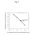
- Figure 3 illustrates the relationship between the ratio between the introduction rates of the hydrogen gas (H 2 ) and the carbon source gas (C 2 F 6 ) and the wall surface area of the grown carbon nanowall.
- Figure 6 illustrates the relationship between the hydrogen gas (H 2 ) introduction rate and the crystallinity of the carbon nanowall as determined from Raman spectroscopy.
- the degree of crystallinity was approximated by using as an index the D band half value width in the Raman spectrum measured with an irradiation laser wavelength of 514.5 nm. Crystallinity increases as D band half value width decreases. Specifically, by decreasing the H 2 introduction rate, the crystallinity of the carbon nanowall can be increased.
- the D band half value width of the conventional carrier Ketjen black and the D band half value width of graphite were also added. It can be seen that even a carbon nanowall can be made to have a high crystallinity equal to or higher than that of Ketjen black.
- the carbon nanowall according to the present invention has an increased amount of supported catalyst because of its large surface area, and has high conductivity and excellent corrosion resistance against high potential because of its high crystallinity.
- This carbon nanowall is thus especially suitable as an electrode catalyst carrier for a fuel cell. Accordingly, this carbon nanowall will contribute to the practical use and spread of fuel cells.
Landscapes
- Chemical & Material Sciences (AREA)
- Engineering & Computer Science (AREA)
- Nanotechnology (AREA)
- Materials Engineering (AREA)
- Organic Chemistry (AREA)
- Chemical Kinetics & Catalysis (AREA)
- General Chemical & Material Sciences (AREA)
- General Physics & Mathematics (AREA)
- Condensed Matter Physics & Semiconductors (AREA)
- Crystallography & Structural Chemistry (AREA)
- Electrochemistry (AREA)
- Physics & Mathematics (AREA)
- Manufacturing & Machinery (AREA)
- Composite Materials (AREA)
- Inorganic Chemistry (AREA)
- Carbon And Carbon Compounds (AREA)
- Catalysts (AREA)
- Inert Electrodes (AREA)
Abstract
Description
- The present invention relates to a method for controlling a carbon nanowall structure, and to a novel carbon nanowall obtainable by this method which has a controlled structure, such as surface area and crystallinity.
- Known examples of carbonaceous porous materials having a nano-size structure include graphite and amorphous, such as fullerene, carbon nanotubes, carbon nanohorns, and carbon nanoflakes.
- Among carbonaceous porous materials having a nano-size structure, carbon nanowalls (CNW) are a two-dimensional carbon nanostructure which typically have a wall-like structure in which the walls rise upwards from the surface of a substrate in a substantially uniform direction. Fullerene (such as C60) is a zero-dimensional carbon nanostructure. Carbon nanotubes can be considered to be a one-dimensional carbon nanostructure. Carbon nanoflakes are an aggregate of planar, two-dimensional, small pieces similar to carbon nanowalls. Like rose petals, the individual small pieces are not connected to each other so that their carbon nanostructure has an inferior directionality with respect to the substrate to that of carbon nanowalls. Thus, carbon nanowalls have a carbon nanostructure with totally different characteristics from fullerene, carbon nanotubes, carbon nanohoms, and carbon nanoflakes.
- The present inventors have already disclosed a production method and production apparatus focusing on carbon nanowalls in
JP Patent Publication (Kokai) No. 2005-97113A Figure 7 , asource gas 32 containing at least carbon as a constituent element is introduced into areaction chamber 10. Thereaction chamber 10 is provided with a parallel plate capacitively coupled plasma (CCP)generating mechanism 20 which includes afirst electrode 22 and asecond electrode 24. In this way, electromagnetic waves such as RF waves are irradiated to form aplasma atmosphere 34 in which thesource gas 32 has been turned into plasma. On the other hand, in aradical generating chamber 41 provided externally to thereaction chamber 10, aradical source gas 36 containing at least hydrogen is decomposed by RF waves or the like to generatehydrogen radicals 38. Thehydrogen radicals 38 are injected into theplasma atmosphere 34, and carbon nanowalls form on the surface of asubstrate 15 arranged on thesecond electrode 24. - Although the existence of carbon nanowalls (CNW) and several basic production methods thereof are known, a method for controlling a structure so as to produce the optimum shape and physical properties of a carbon nanowall (CNW) according to its use and application has until now been unclear.
- Accordingly, it is an object of the present invention to provide a method for controlling a carbon nanowall (CNW) structure having improved corrosion resistance against high potential by varying the spacing between the carbon nanowall walls so that its surface area and crystallinity are controlled; and to provide a carbon nanowall (CNW) with a high surface area and a carbon nanowall (CNW) with a high crystallinity both of which have a controlled structure.
- The present inventors discovered that by varying the ratio between the introduction rates of process gases in the carbon nanowall (CNW) production process by plasma CVD, the spacing between the carbon nanowall (CNW) walls can be varied, which allows the structure, such as surface area and crystallinity, of the carbon nanowall to be controlled, thereby arriving at the present invention.
- Specifically, first, the present invention is an invention of a carbon nanowall having a controlled structure, such as shape and physical properties, as in the following (1) to (3).
- (1) A high-surface-area carbon nanowall having a wall surface area of 50 cm2/cm2-substrate·µm or more. (Here, "wall surface area" is the wall surface area per unit substrate surface area per unit wall height.) For example, when the carbon nanowall is used as an electrode catalyst carrier for a fuel cell, it is preferred to have a larger surface area as the amount of supported catalyst increases. A carbon nanowall having a wall surface area of 50 cm2/cm2-substrate·µm or more is preferable, a carbon nanowall having a wall surface area of 60 cm2/cm2-substrate·µm or more is more preferable, and a carbon nanowall having a wall surface area of 70 cm2/cm2-substrate·µm or more is even more preferable.
- (2) A carbon nanowall having a crystallinity such that the D band half value width in the Raman spectrum measured with an irradiation laser wavelength of 514.5 nm is 85 cm-1 or less. For example, when using the carbon nanowall as an electronic material for which emphasis is placed on the magnitude of conductivity, higher crystallinity provides higher conductivity and superior corrosion resistance against high potential. Therefore, a carbon nanowall having a crystallinity such that the D band half value width in the Raman spectrum is 85 cm-1 or less is preferable, a carbon nanowall having a crystallinity such that the D band half value width in the Raman spectrum is 65 cm-1 or less is more preferable, and a carbon nanowall having a crystallinity such that the D band half value width in the Raman spectrum is 50 cm-1 or less is even more preferable.
- (3) A carbon nanowall which combines high surface area and high crystallinity, having not only a wall surface area of 50 cm2/cm2-substrate·µm or more but also a crystallinity such that the D-band half value width in the Raman spectrum measured with an irradiation laser wavelength of 514.5 nm is 85 cm-1 or less. This carbon nanowall has an increased amount of supported catalyst because of its large surface area, and has high conductivity and excellent corrosion resistance against high potential because of its high crystallinity, and is thus especially suitable as an electrode catalyst carrier for a fuel cell.
- Second, the present invention is an invention of a method for controlling a carbon nanowall structure having a controlled structural shape and physical properties such as surface area and crystallinity, wherein, in a method for producing a carbon nanowall by forming in at least a part of a reaction chamber a plasma atmosphere in which a carbon source gas having at least carbon as a constituent element has been turned into plasma, injecting into the plasma atmosphere hydrogen radicals generated externally to the atmosphere from H2 gas, and forming a carbon nanowall on a surface of a substrate provided in the reaction chamber by reacting the plasma and the hydrogen radicals, a ratio between introduction rates of the H2 gas and the carbon source gas as a design factor controls the surface area and/or crystallinity of the produced carbon nanowall.
- It is noted that the absolute value of the wall surface area is determined by the ratio between the introduction rates of the H2 gas and the carbon source gas (H2 gas introduction rate (mol)/carbon source gas introduction rate (mol)), which is a design factor in the present invention, as well as by the values of other design factors. However, in the present specification, the ratio between the introduction rates is discussed with a substrate temperature of 970°C, chamber internal pressure of 800 mTorr, substrate material made of silicon, and a plasma generating source power of 13.56 MHz and 100 W as such other design factors.
- Here, the design factor which is the ratio between the introduction rates of the H2 gas and the carbon source gas (H2 gas introduction rate (mol)/carbon source gas introduction rate (mol) can be varied over a broad range according to the shape and physical properties, such as surface area and crystallinity, of the desired carbon nanowall. Generally, although the ratio between the introduction rates of the H2 gas and the carbon source gas (H2 gas introduction rate (mol)/carbon source gas introduction rate (mol)) can be varied by up to about 0.5 to 3, practically a carbon nanowall can be formed when this ratio is 1 to 2.5.
- Specifically, by setting the ratio between the introduction rates of the H2 gas and the carbon source gas (H2 gas introduction rate (mol)/carbon source gas introduction rate (mol)) to 1.8 or less, a carbon nanowall can be formed having a wall surface area of 50 cm2/cm2-substrate·µm or more. By setting the ratio between the introduction rates of the H2 gas and the carbon source gas (H2 gas introduction rate (mol)/carbon source gas introduction rate (mol)) to 1.4 or less, a carbon nanowall can be formed having a surface area of 60 cm2/cm2-substrate·µm or more, and by setting the ratio between the introduction rates of the H2 gas and the carbon source gas (H2 gas introduction rate (mol)/carbon source gas introduction rate (mol)) to 1.0 or less, a carbon nanowall can be formed having a surface area of 70 cm2/cm2-substrate·µm or more.
- Further, by setting the H2 gas introduction rate at a 2.5 sccm/cm2-parallel plate electrode surface area or more, a carbon nanowall can be formed having a crystallinity such that the D band half value width in the Raman spectrum is 85 cm-1 or less; by setting the H2 gas introduction rate to a 4.2 sccm/cm2-parallel plate electrode surface area or more, a carbon nanowall can be formed having a crystallinity such that the D band half value width in the Raman spectrum is 65 cm-1 or less, and by setting the H2 gas introduction rate to 5.8 sccm/cm2-parallel plate electrode surface area or more, a carbon nanowall can be formed having a crystallinity such that the D band half value width in the Raman spectrum is 50 cm-1 or less.
- In the present invention, examples of methods for generating the hydrogen radicals from the H2 gas include irradiating one or more selected from microwaves, UHF waves, VHF waves, and RF waves on the H2 gas, and causing the H2 gas to come into contact with a heated catalyst metal.
- In the present invention, examples of the starting material for the carbon source gas include compounds having at least carbon and hydrogen as constituent elements and compounds having at least carbon and fluorine as constituent elements.
- Third, the present invention is a catalyst layer for a fuel cell, characterized in that a carrier for the catalyst layer is the above-described carbon nanowall having a controlled structure, and that a catalyst component and/or electrolyte component is supported/dispersed on the carrier for the catalyst layer composed of the carbon nanowall. By using a carbon nanowall having both a high surface area and high crystallinity as the electrode catalyst carrier for a fuel cell, such an electrode catalyst carrier has an increased amount of supported catalyst because of the large surface area of the carbon nanowall, and has high conductivity and excellent corrosion resistance against high potential because of the high crystallinity of the carbon nanowall, and is thus especially suitable as an electrode catalyst carrier for a fuel cell.
- By varying the ratio between the introduction rates of the process gases in a carbon nanowall (CNW) production process by plasma CVD, the spacing between the carbon nanowall (CNW) walls can be varied, which allows the surface area and crystallinity to be controlled. The carbon nanowall according to the present invention has an increased amount of supported catalyst because of its large surface area, as well as high conductivity and excellent corrosion resistance against high potential because of its high crystallinity, and is thus especially suitable as an electrode catalyst carrier for a fuel cell.
-
-
Figure 1 illustrates a schematic view of one example of an apparatus for forming a carbon nanowall having a controlled structure according to the present invention. -
Figure 2 illustrates a schematic view of an apparatus for forming the carbon nanowall used in the examples. -
Figure 3 illustrates the relationship between the ratio between the introduction rates of the hydrogen gas (H2) and the carbon source gas (C2F6) and the wall surface area of the grown carbon nanowall. -
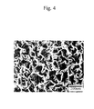
Figure 4 shows a surface SEM photographic image of a carbon nanowall when H2 introduction rate/C2F6 introduction rate = 2. -
Figure 5 shows a surface SEM photographic image of a carbon nanowall when H2 introduction rate/C2F6 introduction rate = 1. -
Figure 6 illustrates the relationship between the hydrogen gas (H2) introduction rate and the crystallinity of the carbon nanowall as determined from Raman spectroscopy. -
Figure 7 illustrates one example of a carbon nanowall control apparatus. - The reference numerals in the drawings are as follows:
- 1
- Plasma CVD apparatus
- 2
- Silicon (Si substrate
- 3
- Heater inside the chamber
- 4
- Plate electrode parallel to the
substrate 2 - 5
- Carbon source gas inlet tube
- 6
- hydrogen gas (H2) inlet tube
- 7
- Plasma generating source
- 8
- Inductive plasma generating source
- 9
- High frequency power apparatus
- 10
- Reaction chamber
- 15
- Carbon source gas inlet tube
- 20
- Plasma discharge means
- 22
- First electrode
- 24
- Second electrode
- 32
- Source gas (raw material)
- 34
- Plasma atmosphere
- 36
- Radical source gas (radical source material)
- 38
- Radical
- 41
- Radical generating chamber
-
Figure 1 illustrates a schematic view of one example of an apparatus for forming a carbon nanowall having a controlled structure according to the present invention. Hydrogen radicals as well as a reaction gas (carbon source gas) containing carbon, such as CF4, C2F6, or CH4, are introduced between parallel plate electrodes in the chamber illustrated inFigure 1 . A carbon nanowall is then formed by PECVD (plasma enhanced chemical vapor deposition). At this stage, the substrate may be heated to approximately 500°C or more. The distance between the parallel plate electrodes is about 5 cm. Between the plate electrodes, a capacitively coupled plasma is generated using a 13.56 MHz high frequency power apparatus with a power of 100 W. The hydrogen radical generation site is a quartz tube with a length of 200 mm and an internal diameter [ϕ] of 26 mm. H2 gas is introduced into the quartz tube to produce an inductively coupled plasma using a 13.56 MHz high frequency power apparatus with a power of 400 W. The flow rate of the carbon source gas and the H2 gas may be appropriately varied. The chamber internal pressure is, for example, 100 mTorr. However, this apparatus is merely one example, and the above description is not to be taken as limiting the experimental conditions, equipment, or the results. - Using the
plasma CVD apparatus 1 illustrated inFigure 2 , asubstrate 2 formed by silicon (Si) was placed on aheater 3 inside the chamber. The carbon source gas (C2F6) was introduced from aninlet tube 5 and hydrogen gas (H2) was introduced from aseparate inlet tube 6 between aplate electrode 4 and thesubstrate 2 which are parallel to each other. At this stage, the temperature of the heater was set to 970°C. - Capacitively coupled plasma was generated between the
plate electrode 4 and thesubstrate 2 with the distance between theplate electrode 4 and thesubstrate 2 set to 5 cm and the output power of theplasma generating source 7 set at 13.56 MHz and 100 W. Further, inductively coupled plasma was generated in theinlet tube 6 by an inductiveplasma generating source 8. The power of the highfrequency power apparatus 9 at this stage was 13.56 MHz and 400 W. The surface area of the parallel plate electrode was 19.625 cm2 (ϕ 50). - A CNW was grown on the
substrate 2 by a plasma CVD method under the above conditions. The growing was carried out with a carbon source gas flow rate of 50 sccm, and a hydrogen gas flow rate divided into 4 levels of 50 (H2 gas introduction rate (mol)/carbon source gas introduction rate (mol) = 1), 70 (H2 gas introduction rate (mol)/carbon source gas introduction rate (mol) = 1.4), 100 (H2 gas introduction rate (mol)/carbon source gas introduction rate (mol) = 2), and 125 sccm (H2 gas introduction rate (mol)/carbon source gas introduction rate (mol) = 2.5). - At this stage, the pressure in the chamber was set to 800 mTorr. Carbon nanowalls grown for 30 minutes in this system had a height of about 300 to 750 nm, and a wall thickness of 10 to 50 nm.
-
Figure 3 illustrates the relationship between the ratio between the introduction rates of the hydrogen gas (H2) and the carbon source gas (C2F6) and the wall surface area of the grown carbon nanowall.Figure 4 shows a surface SEM photographic image of a carbon nanowall when H2 introduction rate/C2F6 introduction rate = 2.Figure 5 shows a surface SEM photographic image of a carbon nanowall when H2 introduction rate/C2F6 introduction rate = 1. - From the results of
Figures 3 to 5 , it can be seen that as the ratio between the introduction rates of the hydrogen gas and the carbon source gas (H2 gas introduction rate (mol)/carbon source gas introduction rate (mol)) decreases, wall spacing is decreased and surface area is increased. - The fact that crystallinity could also be independently controlled was verified using the same CVD process as that of Example 1 while varying the introduction rate of H2 gas.
-
Figure 6 illustrates the relationship between the hydrogen gas (H2) introduction rate and the crystallinity of the carbon nanowall as determined from Raman spectroscopy. The degree of crystallinity was approximated by using as an index the D band half value width in the Raman spectrum measured with an irradiation laser wavelength of 514.5 nm. Crystallinity increases as D band half value width decreases. Specifically, by decreasing the H2 introduction rate, the crystallinity of the carbon nanowall can be increased. InFigure 6 , for reference the D band half value width of the conventional carrier Ketjen black and the D band half value width of graphite were also added. It can be seen that even a carbon nanowall can be made to have a high crystallinity equal to or higher than that of Ketjen black. - The carbon nanowall according to the present invention has an increased amount of supported catalyst because of its large surface area, and has high conductivity and excellent corrosion resistance against high potential because of its high crystallinity. This carbon nanowall is thus especially suitable as an electrode catalyst carrier for a fuel cell. Accordingly, this carbon nanowall will contribute to the practical use and spread of fuel cells.
Claims (9)
- A carbon nanowall, characterized by having a wall surface area of 50 cm2/cm2-substrate·µm or more.
- A carbon nanowall, characterized by having a crystallinity such that the D band half value width in the Raman spectrum measured with an irradiation laser wavelength of 514.5 nm is 85 cm-1 or less.
- A carbon nanowall, characterized by having not only a wall surface area of 50 cm2/cm2-substrate·µm or more but also a crystallinity such that the D-band half value width in the Raman spectrum measured with an irradiation laser wavelength of 514.5 nm is 85 cm-1 or less.
- A method for controlling a carbon nanowall structure, characterized in that in a method for producing a carbon nanowall by forming in at least a part of a reaction chamber a plasma atmosphere in which a carbon source gas having at least carbon as a constituent element has been turned into plasma, injecting into the plasma atmosphere hydrogen radicals generated externally to the atmosphere from H2 gas, and forming a carbon nanowall on a surface of a substrate provided in the reaction chamber by reacting the plasma and the hydrogen radicals, a ratio between introduction rates of the H2 gas and the carbon source gas as a design factor controls the surface area and/or crystallinity of the produced carbon nanowall.
- The method for controlling a carbon nanowall structure according to claim 4, characterized in that the ratio between the introduction rates of the H2 gas and the carbon source gas (H2 gas introduction rate (mol)/carbon source gas introduction rate (mol)) is 1 to 2.5.
- The method for controlling a carbon nanowall structure according to claim 4 or 5, characterized by generating the hydrogen radicals from the H2 gas by irradiating one or more selected from microwaves, UHF waves, VHF waves, and RF waves on the H2 gas, and/or causing the H2 gas to come into contact with a heated catalyst metal.
- The method for controlling a carbon nanowall structure according to any of claims 4 to 6, characterized in that the carbon source gas has at least carbon and hydrogen as constituent elements.
- The method for controlling carbon nanowall structure according to any of claims 4 to 6, characterized in that the carbon source gas has at least carbon and fluorine as constituent elements.
- A catalyst layer for a fuel cell, characterized in that a carrier for the catalyst layer is the carbon nanowall according to any of claims 1 to 3 and that a catalyst component and/or electrolyte component is supported/dispersed on the carrier for the catalyst layer composed of the carbon nanowall.
Applications Claiming Priority (2)
| Application Number | Priority Date | Filing Date | Title |
|---|---|---|---|
| JP2006201927A JP4662067B2 (en) | 2006-07-25 | 2006-07-25 | Structure-controlled carbon nanowall and structure control method of carbon nanowall |
| PCT/JP2007/065036 WO2008013309A1 (en) | 2006-07-25 | 2007-07-25 | Carbon nanowall with controlled structure and method of controlling structure of carbon nanowall |
Publications (3)
| Publication Number | Publication Date |
|---|---|
| EP2048113A1 true EP2048113A1 (en) | 2009-04-15 |
| EP2048113A4 EP2048113A4 (en) | 2010-03-17 |
| EP2048113B1 EP2048113B1 (en) | 2014-02-26 |
Family
ID=38981617
Family Applications (1)
| Application Number | Title | Priority Date | Filing Date |
|---|---|---|---|
| EP07791720.1A Not-in-force EP2048113B1 (en) | 2006-07-25 | 2007-07-25 | Carbon nanowall with controlled structure and method for controlling carbon nanowall structure |
Country Status (6)
| Country | Link |
|---|---|
| US (1) | US20100009242A1 (en) |
| EP (1) | EP2048113B1 (en) |
| JP (1) | JP4662067B2 (en) |
| CN (1) | CN101489926B (en) |
| CA (1) | CA2654430C (en) |
| WO (1) | WO2008013309A1 (en) |
Families Citing this family (21)
| Publication number | Priority date | Publication date | Assignee | Title |
|---|---|---|---|---|
| JP5001995B2 (en) | 2009-11-11 | 2012-08-15 | トヨタ自動車株式会社 | Positive electrode for lithium secondary battery and method for producing the same |
| JP5130275B2 (en) | 2009-11-11 | 2013-01-30 | トヨタ自動車株式会社 | Negative electrode for lithium secondary battery and method for producing the same |
| JP2012041249A (en) * | 2010-08-23 | 2012-03-01 | Nagoya Univ | Manufacturing method for carbon nanostructure |
| JP5886547B2 (en) * | 2011-07-05 | 2016-03-16 | 学校法人中部大学 | Carbon nanowall array and method for producing carbon nanowall |
| JP5834720B2 (en) * | 2011-09-30 | 2015-12-24 | 三菱マテリアル株式会社 | Carbon nanofiber production method and carbon nanofiber dispersion |
| JP5971840B2 (en) * | 2012-02-20 | 2016-08-17 | 株式会社Ihi | Nitrogen introduction method |
| CN103420356A (en) * | 2012-05-22 | 2013-12-04 | 海洋王照明科技股份有限公司 | Method for preparing carbon nanometer walls under normal pressure |
| CN103833022B (en) * | 2012-11-27 | 2016-01-13 | 海洋王照明科技股份有限公司 | Graphene nanobelt and preparation method thereof |
| CN103832999B (en) * | 2012-11-27 | 2015-12-02 | 海洋王照明科技股份有限公司 | Carbon nanometer wall and prepared the method for graphene nanobelt by it |
| CN103879987B (en) * | 2012-12-20 | 2016-01-13 | 海洋王照明科技股份有限公司 | The preparation method of graphene nanobelt |
| CN103879989B (en) * | 2012-12-20 | 2016-01-13 | 海洋王照明科技股份有限公司 | The preparation method of nitrogen-doped graphene nano belt |
| CN103879988A (en) * | 2012-12-20 | 2014-06-25 | 海洋王照明科技股份有限公司 | Boron-doped graphene nano-belt preparation method |
| CN103935981B (en) * | 2013-01-18 | 2016-04-13 | 海洋王照明科技股份有限公司 | Graphene nanobelt and preparation method thereof |
| JP6039534B2 (en) | 2013-11-13 | 2016-12-07 | 東京エレクトロン株式会社 | Carbon nanotube generation method and wiring formation method |
| CA2948832A1 (en) * | 2014-05-13 | 2015-11-19 | Microbial Discovery Group, Llc | Direct-fed microbials and methods of their use |
| CN109250708B (en) * | 2018-12-07 | 2021-01-22 | 四川聚创石墨烯科技有限公司 | System for optical microwave reduction of graphene oxide |
| JP7274747B2 (en) * | 2019-12-20 | 2023-05-17 | 国立大学法人東海国立大学機構 | Manufacturing method of carbon nanowall |
| WO2021201199A1 (en) * | 2020-04-01 | 2021-10-07 | 国立大学法人東海国立大学機構 | Power storage device and electrode for power storage device |
| IT202100017024A1 (en) | 2021-06-29 | 2022-12-29 | Pierfrancesco Atanasio | Carbon/active material hybrid electrodes for lithium ion batteries |
| CN113582162B (en) * | 2021-08-27 | 2023-06-30 | 西安应用光学研究所 | High-optical-absorption carbon nanomaterial and preparation method thereof |
| CN118943377B (en) * | 2024-07-18 | 2025-05-06 | 江阴纳力新材料科技有限公司 | Composite current collector, pole piece and secondary battery using the same |
Family Cites Families (3)
| Publication number | Priority date | Publication date | Assignee | Title |
|---|---|---|---|---|
| EP1661855A4 (en) * | 2003-08-27 | 2012-01-18 | Mineo Hiramatsu | Carbon nanowall producing method, carbon nanowall, and production apparatus |
| US7511415B2 (en) * | 2004-08-26 | 2009-03-31 | Dialight Japan Co., Ltd. | Backlight for liquid crystal display device |
| JP2005097113A (en) * | 2004-11-26 | 2005-04-14 | Mineo Hiramatsu | Carbon nanowall manufacturing method and manufacturing apparatus |
-
2006
- 2006-07-25 JP JP2006201927A patent/JP4662067B2/en active Active
-
2007
- 2007-07-25 CN CN2007800263113A patent/CN101489926B/en not_active Expired - Fee Related
- 2007-07-25 US US12/374,844 patent/US20100009242A1/en not_active Abandoned
- 2007-07-25 CA CA2654430A patent/CA2654430C/en not_active Expired - Fee Related
- 2007-07-25 EP EP07791720.1A patent/EP2048113B1/en not_active Not-in-force
- 2007-07-25 WO PCT/JP2007/065036 patent/WO2008013309A1/en not_active Ceased
Also Published As
| Publication number | Publication date |
|---|---|
| JP2008024570A (en) | 2008-02-07 |
| US20100009242A1 (en) | 2010-01-14 |
| CA2654430A1 (en) | 2008-01-31 |
| CN101489926A (en) | 2009-07-22 |
| EP2048113B1 (en) | 2014-02-26 |
| CA2654430C (en) | 2011-12-13 |
| WO2008013309A1 (en) | 2008-01-31 |
| EP2048113A4 (en) | 2010-03-17 |
| JP4662067B2 (en) | 2011-03-30 |
| CN101489926B (en) | 2013-05-15 |
Similar Documents
| Publication | Publication Date | Title |
|---|---|---|
| EP2048113B1 (en) | Carbon nanowall with controlled structure and method for controlling carbon nanowall structure | |
| EP3802418B1 (en) | Methods for forming carbon nanostructured materials | |
| Wang et al. | Low-temperature plasma synthesis of carbon nanotubes and graphene based materials and their fuel cell applications | |
| US8101526B2 (en) | Method of making diamond nanopillars | |
| US7794797B2 (en) | Synthesis of carbon nanotubes by selectively heating catalyst | |
| Vizireanu et al. | Plasma techniques for nanostructured carbon materials synthesis. A case study: carbon nanowall growth by low pressure expanding RF plasma | |
| JP4855758B2 (en) | Method for producing diamond having acicular protrusion arrangement structure on surface | |
| JP3962420B2 (en) | Carbon nanowall manufacturing method, carbon nanowall and manufacturing apparatus | |
| JP2012041249A (en) | Manufacturing method for carbon nanostructure | |
| Gordillo‐Vazquez et al. | From carbon nanostructures to new photoluminescence sources: An Overview of new perspectives and emerging applications of low‐pressure PECVD | |
| KR20110056400A (en) | Low Pressure High Frequency Pulsed Plasma Reactor for Nanoparticles | |
| JP2009091234A (en) | Substrate on which conductive diamond film is formed and method for manufacturing substrate on which conductive diamond film is formed | |
| JP2008239357A (en) | Method for manufacturing carbon nanowall | |
| KR20150113164A (en) | Oxygen reduction catalyst, oxygen reduction electrode, and fuel cell | |
| JP2007230863A (en) | Carbon nanowall | |
| Batryshev et al. | Investigation of synthesis of carbon nanowalls by the chemical vapor deposition method in the plasma of a radio frequency capacitive discharge | |
| US20060276055A1 (en) | Method of forming an oxygen- or nitrogen-terminated silicon nanocrystalline structure and an oxygen- or nitrogen-terminated silicon nanocrystalline structure formed by the method | |
| CN111203248A (en) | Preparation method of doped graphene-coated transition metal carbide nanocapsule and application of doped graphene-coated transition metal carbide nanocapsule in microwave catalysis | |
| JP4975289B2 (en) | Electronic devices using carbon nanowalls | |
| JP5028593B2 (en) | Method for producing transparent conductive film | |
| US12559373B2 (en) | Graphene nanowalls, manufacturing method thereof, electrode and supercapacitor | |
| JP2002339072A (en) | Thin film deposition method and thin film deposition apparatus | |
| CN118234888A (en) | Method for depositing graphene or graphene oxide directly onto a substrate of interest | |
| Yang et al. | Enhanced Field Electron Emission Properties of Hybrid Carbon Nanotubes Synthesized by RF‐PECVD | |
| JPH01246364A (en) | Vapor-phase synthesis for hydrofluorinated amorphous silicon carbide thin film and fluorinated amorphous silicon thin film |
Legal Events
| Date | Code | Title | Description |
|---|---|---|---|
| PUAI | Public reference made under article 153(3) epc to a published international application that has entered the european phase |
Free format text: ORIGINAL CODE: 0009012 |
|
| 17P | Request for examination filed |
Effective date: 20090225 |
|
| AK | Designated contracting states |
Kind code of ref document: A1 Designated state(s): AT BE BG CH CY CZ DE DK EE ES FI FR GB GR HU IE IS IT LI LT LU LV MC MT NL PL PT RO SE SI SK TR |
|
| AX | Request for extension of the european patent |
Extension state: AL BA HR MK RS |
|
| DAX | Request for extension of the european patent (deleted) | ||
| RBV | Designated contracting states (corrected) |
Designated state(s): DE FR GB IT |
|
| A4 | Supplementary search report drawn up and despatched |
Effective date: 20100212 |
|
| RTI1 | Title (correction) |
Free format text: CARBON NANOWALL WITH CONTROLLED STRUCTURE AND METHOD FOR CONTROLLING CARBON NANOWALL STRUCTURE |
|
| 17Q | First examination report despatched |
Effective date: 20110404 |
|
| RAP1 | Party data changed (applicant data changed or rights of an application transferred) |
Owner name: TOYOTA JIDOSHA KABUSHIKI KAISHA |
|
| RIC1 | Information provided on ipc code assigned before grant |
Ipc: H01M 4/92 20060101ALI20130705BHEP Ipc: B82Y 40/00 20110101ALI20130705BHEP Ipc: B01J 21/18 20060101ALI20130705BHEP Ipc: H01M 4/90 20060101ALI20130705BHEP Ipc: B01J 32/00 20060101ALI20130705BHEP Ipc: H01M 4/96 20060101ALI20130705BHEP Ipc: B82Y 30/00 20110101ALI20130705BHEP Ipc: C01B 31/02 20060101AFI20130705BHEP |
|
| GRAP | Despatch of communication of intention to grant a patent |
Free format text: ORIGINAL CODE: EPIDOSNIGR1 |
|
| INTG | Intention to grant announced |
Effective date: 20130912 |
|
| GRAS | Grant fee paid |
Free format text: ORIGINAL CODE: EPIDOSNIGR3 |
|
| GRAA | (expected) grant |
Free format text: ORIGINAL CODE: 0009210 |
|
| RIN1 | Information on inventor provided before grant (corrected) |
Inventor name: SUGIYAMA, TORU Inventor name: HAMA, YUICHIRO Inventor name: HORI, MASARU Inventor name: HIRAMATSU, MINEO Inventor name: KANO, HIROYUKI |
|
| AK | Designated contracting states |
Kind code of ref document: B1 Designated state(s): DE FR GB IT |
|
| REG | Reference to a national code |
Ref country code: GB Ref legal event code: FG4D |
|
| REG | Reference to a national code |
Ref country code: DE Ref legal event code: R096 Ref document number: 602007035232 Country of ref document: DE Effective date: 20140410 |
|
| RIN2 | Information on inventor provided after grant (corrected) |
Inventor name: HORI, MASARU Inventor name: HAMA, YUICHIRO Inventor name: KANO, HIROYUKI Inventor name: HIRAMATSU, MINEO Inventor name: SUGIYAMA, TORU |
|
| REG | Reference to a national code |
Ref country code: DE Ref legal event code: R097 Ref document number: 602007035232 Country of ref document: DE |
|
| PLBE | No opposition filed within time limit |
Free format text: ORIGINAL CODE: 0009261 |
|
| STAA | Information on the status of an ep patent application or granted ep patent |
Free format text: STATUS: NO OPPOSITION FILED WITHIN TIME LIMIT |
|
| 26N | No opposition filed |
Effective date: 20141127 |
|
| REG | Reference to a national code |
Ref country code: DE Ref legal event code: R097 Ref document number: 602007035232 Country of ref document: DE Effective date: 20141127 |
|
| GBPC | Gb: european patent ceased through non-payment of renewal fee |
Effective date: 20140725 |
|
| PG25 | Lapsed in a contracting state [announced via postgrant information from national office to epo] |
Ref country code: IT Free format text: LAPSE BECAUSE OF FAILURE TO SUBMIT A TRANSLATION OF THE DESCRIPTION OR TO PAY THE FEE WITHIN THE PRESCRIBED TIME-LIMIT Effective date: 20140226 |
|
| REG | Reference to a national code |
Ref country code: DE Ref legal event code: R084 Ref document number: 602007035232 Country of ref document: DE |
|
| REG | Reference to a national code |
Ref country code: FR Ref legal event code: ST Effective date: 20150331 |
|
| PG25 | Lapsed in a contracting state [announced via postgrant information from national office to epo] |
Ref country code: FR Free format text: LAPSE BECAUSE OF NON-PAYMENT OF DUE FEES Effective date: 20140731 Ref country code: GB Free format text: LAPSE BECAUSE OF NON-PAYMENT OF DUE FEES Effective date: 20140725 |
|
| REG | Reference to a national code |
Ref country code: DE Ref legal event code: R084 Ref document number: 602007035232 Country of ref document: DE Effective date: 20150417 |
|
| REG | Reference to a national code |
Ref country code: DE Ref legal event code: R079 Ref document number: 602007035232 Country of ref document: DE Free format text: PREVIOUS MAIN CLASS: C01B0031020000 Ipc: C01B0032050000 |
|
| PGFP | Annual fee paid to national office [announced via postgrant information from national office to epo] |
Ref country code: DE Payment date: 20190710 Year of fee payment: 13 |
|
| REG | Reference to a national code |
Ref country code: DE Ref legal event code: R119 Ref document number: 602007035232 Country of ref document: DE |
|
| PG25 | Lapsed in a contracting state [announced via postgrant information from national office to epo] |
Ref country code: DE Free format text: LAPSE BECAUSE OF NON-PAYMENT OF DUE FEES Effective date: 20210202 |