EP2045912A1 - Method and system for using a microstrip to switch circuits in CMOS applications - Google Patents
Method and system for using a microstrip to switch circuits in CMOS applications Download PDFInfo
- Publication number
- EP2045912A1 EP2045912A1 EP08015120A EP08015120A EP2045912A1 EP 2045912 A1 EP2045912 A1 EP 2045912A1 EP 08015120 A EP08015120 A EP 08015120A EP 08015120 A EP08015120 A EP 08015120A EP 2045912 A1 EP2045912 A1 EP 2045912A1
- Authority
- EP
- European Patent Office
- Prior art keywords
- signal
- frequency
- microstrip
- filter
- programmable
- Prior art date
- Legal status (The legal status is an assumption and is not a legal conclusion. Google has not performed a legal analysis and makes no representation as to the accuracy of the status listed.)
- Granted
Links
- 238000000034 method Methods 0.000 title claims abstract description 29
- 238000004891 communication Methods 0.000 claims description 22
- 238000001914 filtration Methods 0.000 claims description 9
- 238000012545 processing Methods 0.000 claims description 4
- 238000013519 translation Methods 0.000 claims description 2
- 239000000758 substrate Substances 0.000 description 13
- 238000010586 diagram Methods 0.000 description 12
- 239000000463 material Substances 0.000 description 9
- 238000002161 passivation Methods 0.000 description 9
- 230000005684 electric field Effects 0.000 description 6
- 238000006243 chemical reaction Methods 0.000 description 5
- 238000001228 spectrum Methods 0.000 description 5
- VYPSYNLAJGMNEJ-UHFFFAOYSA-N Silicium dioxide Chemical compound O=[Si]=O VYPSYNLAJGMNEJ-UHFFFAOYSA-N 0.000 description 4
- 238000004590 computer program Methods 0.000 description 4
- 230000004044 response Effects 0.000 description 4
- 238000013461 design Methods 0.000 description 3
- 230000006870 function Effects 0.000 description 3
- 229910004613 CdTe Inorganic materials 0.000 description 2
- 229910004611 CdZnTe Inorganic materials 0.000 description 2
- 229910005533 GaO Inorganic materials 0.000 description 2
- 229910001218 Gallium arsenide Inorganic materials 0.000 description 2
- PNEYBMLMFCGWSK-UHFFFAOYSA-N aluminium oxide Inorganic materials [O-2].[O-2].[O-2].[Al+3].[Al+3] PNEYBMLMFCGWSK-UHFFFAOYSA-N 0.000 description 2
- 230000008859 change Effects 0.000 description 2
- 229910052681 coesite Inorganic materials 0.000 description 2
- 239000004020 conductor Substances 0.000 description 2
- 229910052593 corundum Inorganic materials 0.000 description 2
- 229910052906 cristobalite Inorganic materials 0.000 description 2
- 230000000694 effects Effects 0.000 description 2
- 230000007613 environmental effect Effects 0.000 description 2
- 239000012212 insulator Substances 0.000 description 2
- 238000002955 isolation Methods 0.000 description 2
- 239000002184 metal Substances 0.000 description 2
- 150000004767 nitrides Chemical class 0.000 description 2
- 229910021420 polycrystalline silicon Inorganic materials 0.000 description 2
- 229910052594 sapphire Inorganic materials 0.000 description 2
- 239000010980 sapphire Substances 0.000 description 2
- 239000004065 semiconductor Substances 0.000 description 2
- 238000000926 separation method Methods 0.000 description 2
- 239000000377 silicon dioxide Substances 0.000 description 2
- 229910052682 stishovite Inorganic materials 0.000 description 2
- 229910052905 tridymite Inorganic materials 0.000 description 2
- 229910001845 yogo sapphire Inorganic materials 0.000 description 2
- XLOMVQKBTHCTTD-UHFFFAOYSA-N zinc oxide Inorganic materials [Zn]=O XLOMVQKBTHCTTD-UHFFFAOYSA-N 0.000 description 2
- 238000013459 approach Methods 0.000 description 1
- QVGXLLKOCUKJST-UHFFFAOYSA-N atomic oxygen Chemical compound [O] QVGXLLKOCUKJST-UHFFFAOYSA-N 0.000 description 1
- 230000005540 biological transmission Effects 0.000 description 1
- 239000003990 capacitor Substances 0.000 description 1
- 230000008878 coupling Effects 0.000 description 1
- 238000010168 coupling process Methods 0.000 description 1
- 238000005859 coupling reaction Methods 0.000 description 1
- 230000001419 dependent effect Effects 0.000 description 1
- 238000005516 engineering process Methods 0.000 description 1
- 238000010348 incorporation Methods 0.000 description 1
- 230000001939 inductive effect Effects 0.000 description 1
- 230000010365 information processing Effects 0.000 description 1
- 230000007246 mechanism Effects 0.000 description 1
- 238000002156 mixing Methods 0.000 description 1
- 238000010295 mobile communication Methods 0.000 description 1
- 238000012986 modification Methods 0.000 description 1
- 230000004048 modification Effects 0.000 description 1
- 229910052760 oxygen Inorganic materials 0.000 description 1
- 239000001301 oxygen Substances 0.000 description 1
- 229920005591 polysilicon Polymers 0.000 description 1
- 230000005855 radiation Effects 0.000 description 1
Images



Classifications
-
- H—ELECTRICITY
- H03—ELECTRONIC CIRCUITRY
- H03D—DEMODULATION OR TRANSFERENCE OF MODULATION FROM ONE CARRIER TO ANOTHER
- H03D7/00—Transference of modulation from one carrier to another, e.g. frequency-changing
- H03D7/14—Balanced arrangements
- H03D7/1425—Balanced arrangements with transistors
- H03D7/1441—Balanced arrangements with transistors using field-effect transistors
-
- H—ELECTRICITY
- H01—ELECTRIC ELEMENTS
- H01P—WAVEGUIDES; RESONATORS, LINES, OR OTHER DEVICES OF THE WAVEGUIDE TYPE
- H01P3/00—Waveguides; Transmission lines of the waveguide type
- H01P3/02—Waveguides; Transmission lines of the waveguide type with two longitudinal conductors
- H01P3/08—Microstrips; Strip lines
-
- H—ELECTRICITY
- H01—ELECTRIC ELEMENTS
- H01P—WAVEGUIDES; RESONATORS, LINES, OR OTHER DEVICES OF THE WAVEGUIDE TYPE
- H01P1/00—Auxiliary devices
- H01P1/20—Frequency-selective devices, e.g. filters
- H01P1/201—Filters for transverse electromagnetic waves
- H01P1/203—Strip line filters
-
- H—ELECTRICITY
- H03—ELECTRONIC CIRCUITRY
- H03D—DEMODULATION OR TRANSFERENCE OF MODULATION FROM ONE CARRIER TO ANOTHER
- H03D7/00—Transference of modulation from one carrier to another, e.g. frequency-changing
- H03D7/14—Balanced arrangements
- H03D7/1425—Balanced arrangements with transistors
- H03D7/1433—Balanced arrangements with transistors using bipolar transistors
-
- H—ELECTRICITY
- H03—ELECTRONIC CIRCUITRY
- H03D—DEMODULATION OR TRANSFERENCE OF MODULATION FROM ONE CARRIER TO ANOTHER
- H03D7/00—Transference of modulation from one carrier to another, e.g. frequency-changing
- H03D7/14—Balanced arrangements
- H03D7/1425—Balanced arrangements with transistors
- H03D7/1466—Passive mixer arrangements
-
- H—ELECTRICITY
- H03—ELECTRONIC CIRCUITRY
- H03D—DEMODULATION OR TRANSFERENCE OF MODULATION FROM ONE CARRIER TO ANOTHER
- H03D7/00—Transference of modulation from one carrier to another, e.g. frequency-changing
- H03D7/14—Balanced arrangements
- H03D7/1425—Balanced arrangements with transistors
- H03D7/1483—Balanced arrangements with transistors comprising components for selecting a particular frequency component of the output
-
- H—ELECTRICITY
- H03—ELECTRONIC CIRCUITRY
- H03J—TUNING RESONANT CIRCUITS; SELECTING RESONANT CIRCUITS
- H03J3/00—Continuous tuning
- H03J3/02—Details
- H03J3/06—Arrangements for obtaining constant bandwidth or gain throughout tuning range or ranges
- H03J3/08—Arrangements for obtaining constant bandwidth or gain throughout tuning range or ranges by varying a second parameter simultaneously with the tuning, e.g. coupling bandpass filter
Definitions
- Certain embodiments of the invention relate to wireless communication. More specifically, certain embodiments of the invention relate to a method and system for using a microstrip to switch circuits in CMOS applications.
- the Federal Communications Commission designated a large contiguous block of 7 GHz bandwidth for communications in the 57 GHz to 64 GHz spectrum.
- This frequency band may be used by the spectrum users on an unlicensed basis, that is, the spectrum is accessible to anyone, subject to certain basic, technical restrictions such as maximum transmission power and certain coexistence mechanisms.
- the communications taking place in this band are often referred to as '60 GHz communications'.
- 60 GHz communications is similar to other forms of unlicensed spectrum use, for example Wireless LANs or Bluetooth in the 2.4 GHz ISM bands.
- communications at 60 GHz may be significantly different in aspects other than accessibility.
- 60 GHz signals may provide markedly different communications channel and propagation characteristics, not least due to the fact that 60 GHz radiation is partly absorbed by oxygen in the air, leading to higher attenuation with distance.
- 60 GHz communications are wireless personal area networks, wireless high-definition television signal, for example from a set top box to a display, or Point-to-Point links.
- a method for processing communication signals comprising:
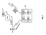
- FIG. 1 is a diagram illustrating an exemplary wireless communication system, in connection with an embodiment of the invention.
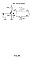
- FIG. 2A is a circuit diagram illustrating an exemplary frequency conversion mixer, in accordance with an embodiment of the invention.
- FIG. 2B is a small signal equivalent circuit illustrating functionality of the frequency conversion mixer, in accordance with an embodiment of the invention.
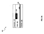
- FIG. 3A is a block diagram illustrating a cross sectional view of a microstrip bandpass filter, in accordance with an embodiment of the invention.
- FIG. 3B is a block diagram of an exemplary microstrip bandpass filter, in accordance with an embodiment of the invention.
- FIG. 3C is a block diagram illustrating a cross sectional view of a coplanar waveguide bandpass filter, in accordance with an embodiment of the invention.
- Fig. 3D is a block diagram of an exemplary coplanar waveguide bandpass filter, in accordance with an embodiment of the invention.
- Certain embodiments of the invention may be found in a method and system for using a microstrip to switch circuits in CMOS applications.
- Aspects of a method and system for a distributed transceiver for high frequency applications may comprise generating a second signal from a first signal by frequency-translating the first signal by switching a first current associated with the first signal between a first signal path and a second signal path.
- the switched first current may be filtered via a microstrip filter that may be tuned to a desired frequency component of the frequency-translated first signal, and the second signal may be generated from the difference between the voltage of the first signal path and the second signal path.
- the microstrip filter may be a programmable bandpass filter or a programmable stopband filter, and the microstrip filter may be tuned to the harmonic frequency by tuning a center frequency of the microstrip filter.
- the center frequency may be configured by adjusting a capacitance and/or an inductance of the microstrip filter.
- the bandwidth of the microstrip bandwidth may be configured.
- the microstrip filter may comprise a programmable coplanar waveguide filter, for which the center frequency may be configured by adjusting a capacitance and/or an inductance of the programmable coplanar waveguide filter.
- the bandwidth of the programmable coplanar waveguide filter may be configured.
- FIG. 1 is a diagram illustrating an exemplary wireless communication system, in connection with an embodiment of the invention.
- an access point 112b there is shown an access point 112b, a computer 110a, a headset 114a, a router 130, the Internet 132 and a web server 134.
- the computer or host device 110a may comprise a wireless radio 111 a, a short-range radio 111 b, a host processor 111c, and a host memory 111 d.
- a wireless connection between the wireless radio 111 a and the access point 112b and a short-range wireless connection between the short-range radio 111 b and the headset 114a.
- computing and communication devices may comprise hardware and software to communicate using multiple wireless communication standards.
- the wireless radio 111a may be compliant with a mobile communications standard, for example.
- the wireless radio 111a and the short-range radio 111 b may be active concurrently.
- the user may establish a wireless connection between the computer 110a and the access point 112b. Once this connection is established, the streaming content from the Web server 134 may be received via the router 130, the access point 112b, and the wireless connection, and consumed by the computer or host device 110a.
- the user of the computer 110a may establish a short-range wireless connection with the headset 114a. Once the short-range wireless connection is established, and with suitable configurations on the computer enabled, the audio portion of the streaming content may be consumed by the headset 114a.
- the radio frequency (RF) generation may support fast-switching to enable support of multiple communication standards and/or advanced wideband systems like, for example, Ultrawideband (UWB) radio.
- Other applications of short-range communications may be wireless High-Definition TV (W-HDTV), from a set top box to a video display, for example. W-HDTV may require high data rates that may be achieved with large bandwidth communication technologies, for example UWB and/or 60-GHz communications.
- FIG. 2A is a circuit diagram illustrating an exemplary frequency conversion mixer, in accordance with an embodiment of the invention.
- FETs 202, 204 and 206 there is shown FETs 202, 204 and 206, and a microstrip 208.
- an input signal VIN a drain-source voltage across FET 202 VDS
- a current I1 local oscillator input signal fLO and -fLO
- output signals VO+ and VO- and a DC bias voltage VBB.
- the drain of the FET 202 may be communicatively coupled to the microstrip 208 and the sources of the FETs 204 and 206.
- the source of the FET 202 may be communicatively coupled, for example, to ground.
- the circuit in FIG. 2A may be enabled to mix an input signal VIN with a local oscillator signal fLO and generate a differential output signal at VO+ and VO-.
- RF radio frequency
- the microstrip 208 may comprise suitable logic, circuitry and/or code that may be enabled to generate a programmable, frequency-dependent impedance.
- the microstrip 208 may be of very small impedance for low and high frequencies and may be of a very high impedance at some intermediate frequency w ⁇ .
- the microstrip 208 may be of a large impedance in a narrow band of frequencies around the center frequency w ⁇ , its bandwidth.
- the FETs 204 and 206 may be enabled to operate essentially as switches as may be described for FIG. 2B in more detail.
- the signal amplitude A of fLO may be much larger than the voltage required to switch the FETs 204 and 206 from on to off and vice versa.
- the FET switches 204 and 206 may be in opposite states at a given time instance.
- the FET 204 may be similar to a closed switch when FET 206 may be similar to an open switch, and vice versa.
- the switches generated by the FET 204 and FET 206 may lead to the current I1 to be either flowing from VO+ through FET 204, or from VO- through FET 206 at any given instance in time.
- the DC voltage VBB may be used to bias the circuit illustrated in FIG. 2A . Since, as described above, the microstrip 208 may be of very low impedance at low frequencies, there will be almost no voltage drop across the microstrip 208 for the bias voltage VBB and the drain of the FET 202 will be DC-biased to approximately VBB.
- FIG. 2B is a small signal equivalent circuit illustrating functionality of the frequency conversion mixer, in accordance with an embodiment of the invention.
- the FET small signal model 202 may be a model for the FET 202
- the FET models 204 and 206 may be a model for the FETs 204 and 206, respectively, as illustrated in FIG. 2A .
- the FET small signal model 202 may comprise a current source 202a and an output impedance 202b.
- the FET model 204 may comprise an impedance 204a and a switch 204b.
- the FET model 206 may comprise an impedance 206a and a switch 206b.
- Vds the small signal current i1
- the local oscillator signals fLO and -fLO the small signal output signals Vo+ and Vo-.
- the impedances 210 and 212 may not be communicatively coupled to the circuit and are shown for illustrative purposes only, hence the dotted connection.
- the impedances 210 and 212 may represent, for example, or a further mixing stage, a differential signal amplifier.
- the current i1 may be a function of the input voltage Vin.
- the FETs 204 and 206 may be described as switches, in series with an output impedance 204a and 206a, respectively. Since FET 204 may be controlled by fLO and FET 206 may be controlled by -fLO, the switch 204b may be closed when the switch 206b may be open, and vice versa, at any given instance in time.
- the differential signal Vo ( Vo +)-( Vo -). Since the current i1 flows through FET 204 or FET 206 alternatingly, the output voltage Vo may effectively be ⁇ Vds , depending on which FET may be active. Hence, the output voltage Vo may be Vds with its polarity flipped at the rate that the FETs 204 and 206 may switch on and off. The on and off switching at the FETs 204 and 206 may be determined by the frequency fLO. Hence, the differential output signal Vo may effectively be proportional to the input signal Vin, multiplied by a bipolar square-shaped pulse train of fundamental frequency w LO .
- the output signal may comprise sum and difference terms of the input frequency w 0 and the local oscillator frequency w LO plus various other frequency components which may not be desired.
- the desirable signal component may be the component comprising cos( w 0 t - w LO t ).
- the desirable signal component may be the component comprising cos( w 0 t+w LO t ) .
- the microstrip 208 may be used to filter out the undesirable signal components in equation (1).
- any signal component in equation (1) that may be sufficiently far from w ⁇ in frequency may be shortened to ground, since for these frequencies, the impedance Z of the microstrip 208 may be zero.
- a current may still flow through FET 204 and FET 206, due to the controlling signals fLO and -fLO.
- the desired frequency component at w ⁇ may be the only frequency component from equation (1) that may generate a contribution to the differential output signal Vo .
- usage of the microstrip 208 may be advantageous because the DC bias point may remain stable.
- FIG. 3A is a block diagram illustrating a cross-sectional view of a microstrip bandpass filter, in accordance with an embodiment of the invention.
- a microstrip bandpass filter (MS-BPF) 320 may comprise a passivation layer 301, a signal conductive line 303, a ground plane 305, an oxide layer 307 and a substrate 309.
- the passivation layer 301 may comprise an oxide, nitride or other insulating layer that may provide electrical isolation between the signal conductive line 303, the ground plane 305 and other circuitry on the substrate 309.
- the passivation layer 301 may provide protection from environmental factors for the underlying layers of the MS-BPF 320.
- the passivation layer 301 may be selected based on its dielectric constant and its effect on the electric field that may be present between conductive lines.
- the signal conductive line 303 may comprise metal traces embedded in the oxide layer 307. In another embodiment of the invention, the signal conductive line 303 may comprise poly-silicon or other conductive material. The separation and the voltage potential between the signal conductive line 303 and the ground plane 305 may determine the electric field generated therein. In addition, the dielectric constant of the oxide 307 may also determine the electric field between the signal conductive line 303 and the ground plane 305.
- the oxide layer 307 may comprise SiO 2 or other oxide material that may provide a high resistance insulating layer between the signal conductive line 303 and the ground plane 305.
- the oxide layer 307 may provide a means for configuring the electric field between the signal conductive line 303 and the ground plane 305 by the selection of an oxide material with an appropriate dielectric constant.
- the substrate 309 may comprise a semiconductor or insulator material that may provide mechanical support for the MS-BPF 320 and other devices that may be integrated.
- the substrate 309 may comprise Si, GaAs, sapphire, InP, GaO, ZnO, CdTe, CdZnTe and/or Al 2 O 3 , for example, or any other substrate material that may be suitable for integrating microstrip structures.
- an AC signal may be applied across the signal conductive line 303 and the ground plane 305.
- the spacing between the conductive line 303 and the ground plane 305, as well as the pattern of the conductive lines, may generate an inductance and a capacitance that may be utilized for filtering purposes, specifically bandpass filtering, in the present invention.
- programmable impedances may be coupled across the microstrip devices in the MS-BFP 320 to tune the center frequency and bandwidth and will be described further with respect to FIG. 3B .
- FIG. 3B is a block diagram of an exemplary microstrip bandpass filter, in accordance with an embodiment of the invention.
- a microstrip bandpass filter 350 comprising three resonator sections 340, 360 and 380, an input coupler 313 and an output coupler 315.
- Each resonator section 340, 360 and 380 may comprise a pattern of signal conductive line 303.
- programmable impedances Z 12 , Z 23 and Z 13 there is shown programmable impedances Z 12 , Z 23 and Z 13 .
- the pattern of signal conductive line 303 is an exemplary embodiment. The invention is not limited to this type of structure, as any number of patterns may be utilized to create a bandpass filter. Changing the shape may change the frequency response of the MS-BPF 350. In this manner, the frequency response may be tuned to a particular range with the design of the signal conductive line 303, and fine tuning may be accomplished by adjusting the programmable impedances Z 12 , Z 23 and Z 13 .
- the signal conductive line 303 may be as described with respect to FIG. 3A .
- the programmable impedances may comprise inductors and/or capacitors that may be programmably adjusted to modify the center frequency and bandwidth of the MS-BPF 350.
- the number and location of the impedances Z 12 , Z 23 and Z 13 is not limited to the configuration shown in FIG. 3B . Accordingly, any number of impedances may be used at multiple locations within the MS-BPF 350.
- the input and output couplers 313 and 315 may comprise inductive tap couplings for communicating signals into and out of the MS-BPF 350, respectively.
- the input and output couplers 313 and 315 may comprise series-capacitance couplers.
- an input signal may be communicated to the MS-BPF 350 via the input coupler 313.
- the desired frequency of operation may be configured by adjusting the impedances of the programmable impedances Z 12 , Z 23 and Z 13 .
- the filtered output signal may be communicated from the output coupler 315.
- tuning may be accomplished by suspending portions of the MS-BPF 350 over the substrate with an air gap. By adjusting this air gap, via piezoelectric or electrostatic means, for example, the capacitance of the structure may be altered, adjusting the bandpass filter frequency.
- FIG. 3C is a block diagram illustrating a cross-sectional view of a coplanar waveguide bandpass filter, in accordance with an embodiment of the invention.
- a coplanar waveguide bandpass filter (CPW-BPF) 300 may comprise a passivation layer 301, a signal conductive line 303A, a ground conductive line 303B, an oxide layer 307 and a substrate 309.
- the passivation layer 301 may comprise an oxide, nitride or other insulating layer that may provide electrical isolation between the conductive lines 303A and 303B and other circuitry on the substrate 309.
- the passivation layer 301 may provide protection from environmental factors for the underlying layers of the CPW-BPF 300.
- the passivation layer 301 may be selected based on its dielectric constant and its effect on the electric field that may be present between conductive lines.
- the signal and ground conductive lines 303A and 303B may comprise metal traces embedded in the oxide layer 307.
- the conductive lines may comprise polysilicon or other conductive material. The separation and the voltage potential between the signal conductive line 303A and the ground conductive line 303B, as well as the dielectric constant of the oxide 307 may determine the electric field generated therein.
- the oxide layer 307 may comprise SiO 2 or other oxide material that may provide a high resistance insulating layer between the signal conductive line 303A and the ground conductive line 303B. In addition, the oxide layer 307 may provide a high resistance insulating layer between the substrate 309 and the conductive lines 303A and 303B.
- the substrate 309 may comprise a semiconductor or insulator material that may provide mechanical support for the CPW-BPF 300 and other devices that may be integrated.
- the substrate 309 may comprise Si, GaAs, sapphire, InP, GaO, ZnO, CdTe, CdZnTe and/or Al 2 O 3 , for example, or any other substrate material that may be suitable for integrating coplanar waveguide structures.
- an AC signal may be applied across the signal conductive line 303A and the ground conductive line 303B.
- the spacing between the conductive lines as well as the pattern of the conductive lines may generate an inductance and a capacitance that may be utilized for filtering purposes, specifically bandpass filtering, in the present invention.
- programmable impedances may be coupled across coplanar waveguide devices in the CPW-BFP 300 to tune the center frequency and bandwidth, and will be described further with respect to FIG. 3D .
- Fig. 3D is a block diagram of an exemplary coplanar waveguide bandpass filter, in accordance with an embodiment of the invention.
- a coplanar waveguide bandpass filter 325 comprising the signal conductive line 303A and the ground conductive line 303B embedded within an oxide layer and covered with a passivation layer as described with respect to FIG. 3C .
- the signal conductive line 303A may be as described with respect to FIG. 3C .
- the pattern of the signal conductive line 303A and the ground conductive line 303B is an exemplary embodiment. The invention is not limited to this type of structure, as any number of patterns may be utilized to create a bandpass filter.
- the CPW-BPF 325 may be designed for a particular frequency range by determining appropriate values for the dimensions d 0 -d 11 .
- an input signal may be communicated to the CPW-BPF 325 at the plus and minus inputs labeled as "In" in FIG. 3D .
- the desired frequency of operation may be configured by the design of the conductive lines 303A and 303B. Changing the shape may change the frequency response of the CPW-BPF 325. In this manner, the frequency response may be tuned to a particular range with the design of the signal conductive line 303A and the ground conductive line 303B. Tuning may be accomplished by adjusting the dimensions of the structure, via switching sections in and out of the structure, for example. In another embodiment of the invention, tuning may be accomplished by suspending portions of the CPW-BPF 325 over the substrate with an air gap.
- the capacitance of the structure may be altered, adjusting the bandpass filter frequency.
- the filtered output signal may be communicated out of the CPW-BPF 325 at the plus and minus outputs labeled as "Out" in FIG. 3D .
- a method and system for using a microstrip to switch circuits in CMOS applications may comprise generating a second signal, for example V o , from a first signal, for example V IN by frequency-translating the first signal by switching a first current, for example i1, associated with the first signal between a first signal path and a second signal path, as shown in FIG. 2A and FIG. 2B .
- the switched first current may be filtered via a microstrip filter, for example microstrip 208, that may be tuned to a desired frequency component of the frequency-translated first signal, for example the sum or difference component, and the second signal may be generated from the difference between the voltage of the first signal path, for example V o +, and the second signal path, for example Vo-.
- a microstrip filter for example microstrip 208
- the second signal may be generated from the difference between the voltage of the first signal path, for example V o +, and the second signal path, for example Vo-.
- the microstrip filter may be a programmable bandpass filter, as described in FIG. 3B , for example, or a programmable stopband filter, and the microstrip filter may be tuned to the harmonic frequency by tuning a center frequency of the microstrip filter, as illustrated in FIG. 3B .
- the center frequency may be configured by adjusting a capacitance and/or an inductance of the microstrip filter, as described for FIG. 3A , FIG. 3B , FIG. 3C and FIG. 3D .
- the bandwidth of the microstrip bandwidth may be configured.
- the microstrip filter may comprise a programmable coplanar waveguide filter, for which the center frequency may be configured by adjusting a capacitance and/or an inductance of the programmable coplanar waveguide filter.
- the bandwidth of the programmable coplanar waveguide filter may be configured.
- Another embodiment of the invention may provide a machine-readable storage, having stored thereon, a computer program having at least one code section executable by a machine, thereby causing the machine to perform the steps as described above for a method and system using a microstrip to switch circuits in CMOS applications.
- the present invention may be realized in hardware, software, or a combination of hardware and software.
- the present invention may be realized in a centralized fashion in at least one computer system, or in a distributed fashion where different elements are spread across several interconnected computer systems. Any kind of computer system or other apparatus adapted for carrying out the methods described herein is suited.
- a typical combination of hardware and software may be a general-purpose computer system with a computer program that, when being loaded and executed, controls the computer system such that it carries out the methods described herein.
- the present invention may also be embedded in a computer program product, which comprises all the features enabling the implementation of the methods described herein, and which when loaded in a computer system is able to carry out these methods.
- Computer program in the present context means any expression, in any language, code or notation, of a set of instructions intended to cause a system having an information processing capability to perform a particular function either directly or after either or both of the following: a) conversion to another language, code or notation; b) reproduction in a different material form.
Landscapes
- Engineering & Computer Science (AREA)
- Power Engineering (AREA)
- Physics & Mathematics (AREA)
- Electromagnetism (AREA)
- Control Of Motors That Do Not Use Commutators (AREA)
- Networks Using Active Elements (AREA)
- Semiconductor Integrated Circuits (AREA)
- Transceivers (AREA)
Abstract
Description
- Not applicable
- Certain embodiments of the invention relate to wireless communication. More specifically, certain embodiments of the invention relate to a method and system for using a microstrip to switch circuits in CMOS applications.
- In 2001, the Federal Communications Commission (FCC) designated a large contiguous block of 7 GHz bandwidth for communications in the 57 GHz to 64 GHz spectrum. This frequency band may be used by the spectrum users on an unlicensed basis, that is, the spectrum is accessible to anyone, subject to certain basic, technical restrictions such as maximum transmission power and certain coexistence mechanisms. The communications taking place in this band are often referred to as '60 GHz communications'. With respect to the accessibility of this part of the spectrum, 60 GHz communications is similar to other forms of unlicensed spectrum use, for example Wireless LANs or Bluetooth in the 2.4 GHz ISM bands. However, communications at 60 GHz may be significantly different in aspects other than accessibility. For example, 60 GHz signals may provide markedly different communications channel and propagation characteristics, not least due to the fact that 60 GHz radiation is partly absorbed by oxygen in the air, leading to higher attenuation with distance. On the other hand, since a very large bandwidth of 7 GHz is available, very high data rates may be achieved. Among the applications for 60 GHz communications are wireless personal area networks, wireless high-definition television signal, for example from a set top box to a display, or Point-to-Point links.
- Further limitations and disadvantages of conventional and traditional approaches will become apparent to one of skill in the art, through comparison of such systems with the present invention as set forth in the remainder of the present application with reference to the drawings.
- A method and/or system for using a microstrip to switch circuits in CMOS applications, substantially as shown in and/or described in connection with at least one of the figures, as set forth more completely in the claims.
According to an aspect, a method is provided for processing communication signals, the method comprising: - generating a second signal from a first signal by:
- frequency-translating said first signal by switching a first current associated with said first signal between a first signal path and a second signal path;
- filtering said switched first current via a microstrip filter tuned to a desired frequency component of said frequency-translated first signal; and
- generating said second signal from the difference between the voltage of said first signal path and said second signal path.
- Advantageously, said microstrip filter is a programmable bandpass filter or a programmable stopband filter.
- Advantageously, said microstrip filter is tuned to said harmonic frequency.
- Advantageously, the method further comprises tuning said harmonic frequency by configuring a center frequency of said microstrip filter.
- Advantageously, the method further comprises adjusting a capacitance of said microstrip filter for said configuring of said center frequency.
- Advantageously, the method further comprises adjusting an inductance of said microstrip filter for said configuring of said center frequency.
- Advantageously, the method further comprises configuring a bandwidth of said microstrip filter.
- Advantageously, said microstrip filter comprises a programmable coplanar waveguide filter.
- Advantageously, the method further comprises configuring a center frequency of said programmable coplanar waveguide filter.
- Advantageously, the method further comprises adjusting a capacitance of said programmable coplanar waveguide filter for said configuring of said center frequency.
- Advantageously, the method further comprises adjusting an inductance of said programmable coplanar waveguide filter for said configuring of said center frequency.
- Advantageously, the method further comprises configuring a bandwidth of said programmable coplanar waveguide filter.
- According to an aspect, a system for processing communication signals comprises:
- one or more circuits, said one or more circuits enabling:
- generation of a second signal from a first signal by:
- frequency-translation of said first signal by switching a first current associated with said first signal between a first signal path and a second signal path;
- filtering of said switched first current via a microstrip filter tuned to a desired frequency component of said frequency-translated first signal; and
- generation of said second signal from the difference between the voltage of said first signal path and said second signal path.
- generation of a second signal from a first signal by:
- Advantageously, said microstrip filter is a programmable bandpass filter or a programmable stopband filter.
- Advantageously, said microstrip filter is tuned to said harmonic frequency.
- Advantageously, said one or more circuits comprise tuning said harmonic frequency by configuring a center frequency of said microstrip filter.
- Advantageously, said one or more circuits adjust a capacitance of said microstrip filter for said configuring of said center frequency.
- Advantageously, said one or more circuits adjust an inductance of said microstrip filter for said configuring of said center frequency.
- Advantageously, said one or more circuits configure a bandwidth of said microstrip filter.
- Advantageously, said microstrip filter comprises a programmable coplanar waveguide filter.
- Advantageously, said one or more circuits configure a center frequency of said programmable coplanar waveguide filter.
- Advantageously, said one or more circuits adjust a capacitance of said programmable coplanar waveguide filter for said configuring of said center frequency.
- Advantageously, said one or more circuits adjust an inductance of said programmable coplanar waveguide filter for said configuring of said center frequency.
- Advantageously, said one or more circuits configure a bandwidth of said programmable coplanar waveguide filter.
- one or more circuits, said one or more circuits enabling:
- These and other advantages, aspects and novel features of the present invention, as well as details of an illustrated embodiment thereof, will be more fully understood from the following description and drawings.
-
FIG. 1 is a diagram illustrating an exemplary wireless communication system, in connection with an embodiment of the invention. -
FIG. 2A is a circuit diagram illustrating an exemplary frequency conversion mixer, in accordance with an embodiment of the invention. -
FIG. 2B is a small signal equivalent circuit illustrating functionality of the frequency conversion mixer, in accordance with an embodiment of the invention. -
FIG. 3A is a block diagram illustrating a cross sectional view of a microstrip bandpass filter, in accordance with an embodiment of the invention. -
FIG. 3B is a block diagram of an exemplary microstrip bandpass filter, in accordance with an embodiment of the invention. -
FIG. 3C is a block diagram illustrating a cross sectional view of a coplanar waveguide bandpass filter, in accordance with an embodiment of the invention. -
Fig. 3D is a block diagram of an exemplary coplanar waveguide bandpass filter, in accordance with an embodiment of the invention. - Certain embodiments of the invention may be found in a method and system for using a microstrip to switch circuits in CMOS applications. Aspects of a method and system for a distributed transceiver for high frequency applications may comprise generating a second signal from a first signal by frequency-translating the first signal by switching a first current associated with the first signal between a first signal path and a second signal path. The switched first current may be filtered via a microstrip filter that may be tuned to a desired frequency component of the frequency-translated first signal, and the second signal may be generated from the difference between the voltage of the first signal path and the second signal path.
- The microstrip filter may be a programmable bandpass filter or a programmable stopband filter, and the microstrip filter may be tuned to the harmonic frequency by tuning a center frequency of the microstrip filter. The center frequency may be configured by adjusting a capacitance and/or an inductance of the microstrip filter. The bandwidth of the microstrip bandwidth may be configured. The microstrip filter may comprise a programmable coplanar waveguide filter, for which the center frequency may be configured by adjusting a capacitance and/or an inductance of the programmable coplanar waveguide filter. The bandwidth of the programmable coplanar waveguide filter may be configured.
-
FIG. 1 is a diagram illustrating an exemplary wireless communication system, in connection with an embodiment of the invention. Referring toFIG. 1 , there is shown anaccess point 112b, acomputer 110a, aheadset 114a, arouter 130, theInternet 132 and aweb server 134. The computer orhost device 110a may comprise awireless radio 111 a, a short-range radio 111 b, ahost processor 111c, and ahost memory 111 d. There is also shown a wireless connection between thewireless radio 111 a and theaccess point 112b, and a short-range wireless connection between the short-range radio 111 b and theheadset 114a. - Frequently, computing and communication devices may comprise hardware and software to communicate using multiple wireless communication standards. The
wireless radio 111a may be compliant with a mobile communications standard, for example. There may be instances when thewireless radio 111a and the short-range radio 111 b may be active concurrently. For example, it may be desirable for a user of the computer orhost device 110a to access theInternet 132 in order to consume streaming content from theWeb server 134. Accordingly, the user may establish a wireless connection between thecomputer 110a and theaccess point 112b. Once this connection is established, the streaming content from theWeb server 134 may be received via therouter 130, theaccess point 112b, and the wireless connection, and consumed by the computer orhost device 110a. - It may be further desirable for the user of the
computer 110a to listen to an audio portion of the streaming content on theheadset 114a. Accordingly, the user of thecomputer 110a may establish a short-range wireless connection with theheadset 114a. Once the short-range wireless connection is established, and with suitable configurations on the computer enabled, the audio portion of the streaming content may be consumed by theheadset 114a. In instances where such advanced communication systems are integrated or located within thehost device 110a, the radio frequency (RF) generation may support fast-switching to enable support of multiple communication standards and/or advanced wideband systems like, for example, Ultrawideband (UWB) radio. Other applications of short-range communications may be wireless High-Definition TV (W-HDTV), from a set top box to a video display, for example. W-HDTV may require high data rates that may be achieved with large bandwidth communication technologies, for example UWB and/or 60-GHz communications. -
FIG. 2A is a circuit diagram illustrating an exemplary frequency conversion mixer, in accordance with an embodiment of the invention. Referring toFIG. 2A , there is shownFETs microstrip 208. There is also shown an input signal VIN, a drain-source voltage acrossFET 202 VDS, a current I1, local oscillator input signal fLO and -fLO, and output signals VO+ and VO-, and a DC bias voltage VBB. - The drain of the
FET 202 may be communicatively coupled to themicrostrip 208 and the sources of theFETs FET 202 may be communicatively coupled, for example, to ground. - The circuit in
FIG. 2A may be enabled to mix an input signal VIN with a local oscillator signal fLO and generate a differential output signal at VO+ and VO-. The input signal VIN may be, for example, a radio frequency (RF) signal, for example VIN = VB +s(t)cos(w 0 t), where VB may be a DC bias voltage component, s(t) may be the information-bearing baseband or intermediate frequency signal and w 0 may be the angular carrier frequency of the RF signal VIN. The local oscillator may be, for example, a sinusoid fLO=Acos(wLOt), or a train of square-shaped pulses at a fundamental frequency wLO . Themicrostrip 208 may comprise suitable logic, circuitry and/or code that may be enabled to generate a programmable, frequency-dependent impedance. For example, themicrostrip 208 may be of very small impedance for low and high frequencies and may be of a very high impedance at some intermediate frequency w µ. Themicrostrip 208 may be of a large impedance in a narrow band of frequencies around the center frequency w µ, its bandwidth. TheFETs FIG. 2B in more detail. The signal amplitude A of fLO may be much larger than the voltage required to switch theFETs FET 204 may be similar to a closed switch whenFET 206 may be similar to an open switch, and vice versa. The switches generated by theFET 204 andFET 206 may lead to the current I1 to be either flowing from VO+ throughFET 204, or from VO- throughFET 206 at any given instance in time. - The DC voltage VBB may be used to bias the circuit illustrated in
FIG. 2A . Since, as described above, themicrostrip 208 may be of very low impedance at low frequencies, there will be almost no voltage drop across themicrostrip 208 for the bias voltage VBB and the drain of theFET 202 will be DC-biased to approximately VBB. -
FIG. 2B is a small signal equivalent circuit illustrating functionality of the frequency conversion mixer, in accordance with an embodiment of the invention. Referring toFIG. 2B , there is shown an FETsmall signal model 202, andFET models small signal model 202 may be a model for theFET 202, theFET models FETs FIG. 2A . The FETsmall signal model 202 may comprise acurrent source 202a and anoutput impedance 202b. TheFET model 204 may comprise animpedance 204a and aswitch 204b. TheFET model 206 may comprise animpedance 206a and aswitch 206b. There is also shown themicrostrip 208 andimpedances - The
impedances impedances - The
FET 202 may generate a current gm·Vin=gm·cos(w0t) in thecurrent source 202a as a function of the input voltage Vin. Hence, the current i1 may be a function of the input voltage Vin. As shown in theFET model FIG. 2A , theFETs output impedance FET 204 may be controlled by fLO andFET 206 may be controlled by -fLO, theswitch 204b may be closed when theswitch 206b may be open, and vice versa, at any given instance in time. The output signal of the mixer illustrated inFIG. 2 may be given by the differential signal Vo=(Vo+)-(Vo-). Since the current i1 flows throughFET 204 orFET 206 alternatingly, the output voltage Vo may effectively be ±Vds , depending on which FET may be active. Hence, the output voltage Vo may be Vds with its polarity flipped at the rate that theFETs FETs microstrip 208 may be a constant, frequency independent impedance:
where the bipolar square wave may be written in terms of its Fourier series expansion. - Hence, as illustrated in the above equation, the output signal may comprise sum and difference terms of the input frequency w 0 and the local oscillator frequency wLO plus various other frequency components which may not be desired. In instances, where the frequency mixer may desire to downconvert a received signal, the desirable signal component may be the component comprising cos(w 0 t-wLOt). In instances where the frequency mixer may desire to upconvert a received signal, the desirable signal component may be the component comprising cos(w 0 t+wLOt).
- The
microstrip 208 may be used to filter out the undesirable signal components in equation (1). The signal in equation (1) may be approximately correct in the case where themicrostrip 208 may be a frequency independent non-zero impedance, as described above. However, the impedance ofmicrostrip 208 may be significantly greater than zero in a narrow bandwidth around the frequency it may be tuned to, wµ . In instances where, for example, themicrostrip 208 may be tuned to wµ = w 0 -wLO, themicrostrip 208 may be essentially similar to a zero impedance (short circuit) for any frequency different from wµ . In this instance, any signal component in equation (1) that may be sufficiently far from wµ in frequency may be shortened to ground, since for these frequencies, the impedance Z of themicrostrip 208 may be zero. In these instances, a current may still flow throughFET 204 andFET 206, due to the controlling signals fLO and -fLO. However, the currents throughFET microstip 208, the final output voltage may be given by the following relationship, when wµ =w 0 -wLO :
- In addition to allowing precise filtering of the desired frequency components, usage of the
microstrip 208 may be advantageous because the DC bias point may remain stable. -
FIG. 3A is a block diagram illustrating a cross-sectional view of a microstrip bandpass filter, in accordance with an embodiment of the invention. Referring toFIG. 3A , there is shown a microstrip bandpass filter (MS-BPF) 320. The MS-BPF 320 may comprise apassivation layer 301, a signalconductive line 303, aground plane 305, anoxide layer 307 and asubstrate 309. - The
passivation layer 301 may comprise an oxide, nitride or other insulating layer that may provide electrical isolation between the signalconductive line 303, theground plane 305 and other circuitry on thesubstrate 309. Thepassivation layer 301 may provide protection from environmental factors for the underlying layers of the MS-BPF 320. In addition, thepassivation layer 301 may be selected based on its dielectric constant and its effect on the electric field that may be present between conductive lines. - The signal
conductive line 303 may comprise metal traces embedded in theoxide layer 307. In another embodiment of the invention, the signalconductive line 303 may comprise poly-silicon or other conductive material. The separation and the voltage potential between the signalconductive line 303 and theground plane 305 may determine the electric field generated therein. In addition, the dielectric constant of theoxide 307 may also determine the electric field between the signalconductive line 303 and theground plane 305. - The
oxide layer 307 may comprise SiO2 or other oxide material that may provide a high resistance insulating layer between the signalconductive line 303 and theground plane 305. In addition, theoxide layer 307 may provide a means for configuring the electric field between the signalconductive line 303 and theground plane 305 by the selection of an oxide material with an appropriate dielectric constant. - The
substrate 309 may comprise a semiconductor or insulator material that may provide mechanical support for the MS-BPF 320 and other devices that may be integrated. Thesubstrate 309 may comprise Si, GaAs, sapphire, InP, GaO, ZnO, CdTe, CdZnTe and/or Al2O3, for example, or any other substrate material that may be suitable for integrating microstrip structures. - In operation, an AC signal may be applied across the signal
conductive line 303 and theground plane 305. The spacing between theconductive line 303 and theground plane 305, as well as the pattern of the conductive lines, may generate an inductance and a capacitance that may be utilized for filtering purposes, specifically bandpass filtering, in the present invention. In addition, programmable impedances may be coupled across the microstrip devices in the MS-BFP 320 to tune the center frequency and bandwidth and will be described further with respect toFIG. 3B . -
FIG. 3B is a block diagram of an exemplary microstrip bandpass filter, in accordance with an embodiment of the invention. Referring toFIG. 3C , there is shown amicrostrip bandpass filter 350 comprising threeresonator sections input coupler 313 and anoutput coupler 315. Eachresonator section conductive line 303. In addition, there is shown programmable impedances Z12, Z23 and Z13. The pattern of signalconductive line 303 is an exemplary embodiment. The invention is not limited to this type of structure, as any number of patterns may be utilized to create a bandpass filter. Changing the shape may change the frequency response of the MS-BPF 350. In this manner, the frequency response may be tuned to a particular range with the design of the signalconductive line 303, and fine tuning may be accomplished by adjusting the programmable impedances Z12, Z23 and Z13. - The signal
conductive line 303 may be as described with respect toFIG. 3A . The programmable impedances may comprise inductors and/or capacitors that may be programmably adjusted to modify the center frequency and bandwidth of the MS-BPF 350. The number and location of the impedances Z12, Z23 and Z13 is not limited to the configuration shown inFIG. 3B . Accordingly, any number of impedances may be used at multiple locations within the MS-BPF 350. - The input and
output couplers BPF 350, respectively. In another embodiment of the invention, the input andoutput couplers - In operation, an input signal may be communicated to the MS-
BPF 350 via theinput coupler 313. The desired frequency of operation may be configured by adjusting the impedances of the programmable impedances Z12, Z23 and Z13. The filtered output signal may be communicated from theoutput coupler 315. In another embodiment of the invention, tuning may be accomplished by suspending portions of the MS-BPF 350 over the substrate with an air gap. By adjusting this air gap, via piezoelectric or electrostatic means, for example, the capacitance of the structure may be altered, adjusting the bandpass filter frequency. -
FIG. 3C is a block diagram illustrating a cross-sectional view of a coplanar waveguide bandpass filter, in accordance with an embodiment of the invention. Referring toFIG. 3C , there is shown a coplanar waveguide bandpass filter (CPW-BPF) 300. The CPW-BPF 300 may comprise apassivation layer 301, a signalconductive line 303A, a groundconductive line 303B, anoxide layer 307 and asubstrate 309. - The
passivation layer 301 may comprise an oxide, nitride or other insulating layer that may provide electrical isolation between theconductive lines substrate 309. Thepassivation layer 301 may provide protection from environmental factors for the underlying layers of the CPW-BPF 300. In addition, thepassivation layer 301 may be selected based on its dielectric constant and its effect on the electric field that may be present between conductive lines. - The signal and ground
conductive lines oxide layer 307. In another embodiment of the invention, the conductive lines may comprise polysilicon or other conductive material. The separation and the voltage potential between the signalconductive line 303A and the groundconductive line 303B, as well as the dielectric constant of theoxide 307 may determine the electric field generated therein. - The
oxide layer 307 may comprise SiO2 or other oxide material that may provide a high resistance insulating layer between the signalconductive line 303A and the groundconductive line 303B. In addition, theoxide layer 307 may provide a high resistance insulating layer between thesubstrate 309 and theconductive lines - The
substrate 309 may comprise a semiconductor or insulator material that may provide mechanical support for the CPW-BPF 300 and other devices that may be integrated. Thesubstrate 309 may comprise Si, GaAs, sapphire, InP, GaO, ZnO, CdTe, CdZnTe and/or Al2O3, for example, or any other substrate material that may be suitable for integrating coplanar waveguide structures. - In operation, an AC signal may be applied across the signal
conductive line 303A and the groundconductive line 303B. The spacing between the conductive lines as well as the pattern of the conductive lines may generate an inductance and a capacitance that may be utilized for filtering purposes, specifically bandpass filtering, in the present invention. In addition, programmable impedances may be coupled across coplanar waveguide devices in the CPW-BFP 300 to tune the center frequency and bandwidth, and will be described further with respect toFIG. 3D . -
Fig. 3D is a block diagram of an exemplary coplanar waveguide bandpass filter, in accordance with an embodiment of the invention. Referring toFIG. 3D , there is shown a coplanarwaveguide bandpass filter 325 comprising the signalconductive line 303A and the groundconductive line 303B embedded within an oxide layer and covered with a passivation layer as described with respect toFIG. 3C . The signalconductive line 303A may be as described with respect toFIG. 3C . The pattern of the signalconductive line 303A and the groundconductive line 303B is an exemplary embodiment. The invention is not limited to this type of structure, as any number of patterns may be utilized to create a bandpass filter. The CPW-BPF 325 may be designed for a particular frequency range by determining appropriate values for the dimensions d0-d11. - In operation, an input signal may be communicated to the CPW-
BPF 325 at the plus and minus inputs labeled as "In" inFIG. 3D . The desired frequency of operation may be configured by the design of theconductive lines BPF 325. In this manner, the frequency response may be tuned to a particular range with the design of the signalconductive line 303A and the groundconductive line 303B. Tuning may be accomplished by adjusting the dimensions of the structure, via switching sections in and out of the structure, for example. In another embodiment of the invention, tuning may be accomplished by suspending portions of the CPW-BPF 325 over the substrate with an air gap. By adjusting this air gap, via piezoelectric or electrostatic means, for example, the capacitance of the structure may be altered, adjusting the bandpass filter frequency. The filtered output signal may be communicated out of the CPW-BPF 325 at the plus and minus outputs labeled as "Out" inFIG. 3D . - In accordance with an embodiment of the invention, a method and system for using a microstrip to switch circuits in CMOS applications may comprise generating a second signal, for example Vo , from a first signal, for example VIN by frequency-translating the first signal by switching a first current, for example i1, associated with the first signal between a first signal path and a second signal path, as shown in
FIG. 2A andFIG. 2B . The switched first current may be filtered via a microstrip filter, forexample microstrip 208, that may be tuned to a desired frequency component of the frequency-translated first signal, for example the sum or difference component, and the second signal may be generated from the difference between the voltage of the first signal path, for example Vo +, and the second signal path, for example Vo-. - The microstrip filter may be a programmable bandpass filter, as described in
FIG. 3B , for example, or a programmable stopband filter, and the microstrip filter may be tuned to the harmonic frequency by tuning a center frequency of the microstrip filter, as illustrated inFIG. 3B . The center frequency may be configured by adjusting a capacitance and/or an inductance of the microstrip filter, as described forFIG. 3A ,FIG. 3B ,FIG. 3C andFIG. 3D . The bandwidth of the microstrip bandwidth may be configured. The microstrip filter may comprise a programmable coplanar waveguide filter, for which the center frequency may be configured by adjusting a capacitance and/or an inductance of the programmable coplanar waveguide filter. The bandwidth of the programmable coplanar waveguide filter may be configured. - Another embodiment of the invention may provide a machine-readable storage, having stored thereon, a computer program having at least one code section executable by a machine, thereby causing the machine to perform the steps as described above for a method and system using a microstrip to switch circuits in CMOS applications.
- Accordingly, the present invention may be realized in hardware, software, or a combination of hardware and software. The present invention may be realized in a centralized fashion in at least one computer system, or in a distributed fashion where different elements are spread across several interconnected computer systems. Any kind of computer system or other apparatus adapted for carrying out the methods described herein is suited. A typical combination of hardware and software may be a general-purpose computer system with a computer program that, when being loaded and executed, controls the computer system such that it carries out the methods described herein.
- The present invention may also be embedded in a computer program product, which comprises all the features enabling the implementation of the methods described herein, and which when loaded in a computer system is able to carry out these methods. Computer program in the present context means any expression, in any language, code or notation, of a set of instructions intended to cause a system having an information processing capability to perform a particular function either directly or after either or both of the following: a) conversion to another language, code or notation; b) reproduction in a different material form.
- While the present invention has been described with reference to certain embodiments, it will be understood by those skilled in the art that various changes may be made and equivalents may be substituted without departing from the scope of the present invention. In addition, many modifications may be made to adapt a particular situation or material to the teachings of the present invention without departing from its scope. Therefore, it is intended that the present invention not be limited to the particular embodiment disclosed, but that the present invention will include all embodiments falling within the scope of the appended claims.
Claims (10)
- A method for processing communication signals, the method comprising:generating a second signal from a first signal by:frequency-translating said first signal by switching a first current associated with said first signal between a first signal path and a second signal path;filtering said switched first current via a microstrip filter tuned to a desired frequency component of said frequency-translated first signal; andgenerating said second signal from the difference between the voltage of said first signal path and said second signal path.
- The method according to claim 1, wherein said microstrip filter is a programmable bandpass filter or a programmable stopband filter.
- The method according to claim 1, wherein said microstrip filter is tuned to said harmonic frequency.
- The method according to claim 3, comprising tuning said harmonic frequency by configuring a center frequency of said microstrip filter.
- The method according to claim 4, comprising adjusting a capacitance of said microstrip filter for said configuring of said center frequency.
- The method according to claim 4, comprising adjusting an inductance of said microstrip filter for said configuring of said center frequency.
- A system for processing communication signals, the system comprising:one or more circuits, said one or more circuits enabling:generation of a second signal from a first signal by:frequency-translation of said first signal by switching a first current associated with said first signal between a first signal path and a second signal path;filtering of said switched first current via a microstrip filter tuned to a desired frequency component of said frequency-translated first signal; andgeneration of said second signal from the difference between the voltage of said first signal path and said second signal path.
- The system according to claim 7, wherein said microstrip filter is a programmable bandpass filter or a programmable stopband filter.
- The system according to claim 7, wherein said microstrip filter is tuned to said harmonic frequency.
- The system according to claim 9, wherein said one or more circuits comprise tuning said harmonic frequency by configuring a center frequency of said microstrip filter.
Applications Claiming Priority (1)
| Application Number | Priority Date | Filing Date | Title |
|---|---|---|---|
| US11/864,771 US8649753B2 (en) | 2007-09-28 | 2007-09-28 | Method and system for using a microstrip to switch circuits in CMOS applications |
Publications (2)
| Publication Number | Publication Date |
|---|---|
| EP2045912A1 true EP2045912A1 (en) | 2009-04-08 |
| EP2045912B1 EP2045912B1 (en) | 2012-10-10 |
Family
ID=40257328
Family Applications (1)
| Application Number | Title | Priority Date | Filing Date |
|---|---|---|---|
| EP08015120A Ceased EP2045912B1 (en) | 2007-09-28 | 2008-08-27 | Method and system for using a microstrip to switch circuits in CMOS applications |
Country Status (5)
| Country | Link |
|---|---|
| US (1) | US8649753B2 (en) |
| EP (1) | EP2045912B1 (en) |
| KR (1) | KR101028055B1 (en) |
| CN (1) | CN101399389B (en) |
| TW (1) | TWI474611B (en) |
Cited By (1)
| Publication number | Priority date | Publication date | Assignee | Title |
|---|---|---|---|---|
| CN113594658A (en) * | 2021-08-11 | 2021-11-02 | 上海交通大学 | Broadband transition structure from grounding coplanar waveguide to suspended microstrip line |
Families Citing this family (2)
| Publication number | Priority date | Publication date | Assignee | Title |
|---|---|---|---|---|
| US6061551A (en) | 1998-10-21 | 2000-05-09 | Parkervision, Inc. | Method and system for down-converting electromagnetic signals |
| US7010286B2 (en) * | 2000-04-14 | 2006-03-07 | Parkervision, Inc. | Apparatus, system, and method for down-converting and up-converting electromagnetic signals |
Citations (4)
| Publication number | Priority date | Publication date | Assignee | Title |
|---|---|---|---|---|
| EP0539133A1 (en) * | 1991-10-23 | 1993-04-28 | Nokia Mobile Phones Ltd. | A transformer |
| US6002860A (en) | 1996-09-27 | 1999-12-14 | Nortel Networks Corporation | High frequency noise and impedance matched integrated circuits |
| EP1278265A2 (en) * | 2001-07-17 | 2003-01-22 | Netro Corporation | Highly integrated planar stacked millimeter wave transceiver |
| US20060273869A1 (en) * | 2005-06-06 | 2006-12-07 | Jachowski Douglas R | Narrow-band absorptive bandstop filter with multiple signal paths |
Family Cites Families (16)
| Publication number | Priority date | Publication date | Assignee | Title |
|---|---|---|---|---|
| US3955161A (en) * | 1974-08-05 | 1976-05-04 | General Dynamics Corporation | Molded waveguide filter with integral tuning posts |
| US4066988A (en) * | 1976-09-07 | 1978-01-03 | Stanford Research Institute | Electromagnetic resonators having slot-located switches for tuning to different frequencies |
| US5142255A (en) * | 1990-05-07 | 1992-08-25 | The Texas A&M University System | Planar active endfire radiating elements and coplanar waveguide filters with wide electronic tuning bandwidth |
| US5908811A (en) * | 1997-03-03 | 1999-06-01 | Das; Satyendranath | High Tc superconducting ferroelectric tunable filters |
| US6879817B1 (en) * | 1999-04-16 | 2005-04-12 | Parkervision, Inc. | DC offset, re-radiation, and I/Q solutions using universal frequency translation technology |
| US6963734B2 (en) * | 1999-12-22 | 2005-11-08 | Parkervision, Inc. | Differential frequency down-conversion using techniques of universal frequency translation technology |
| US7010286B2 (en) * | 2000-04-14 | 2006-03-07 | Parkervision, Inc. | Apparatus, system, and method for down-converting and up-converting electromagnetic signals |
| US20040145954A1 (en) * | 2001-09-27 | 2004-07-29 | Toncich Stanley S. | Electrically tunable bandpass filters |
| KR20040048946A (en) * | 2001-10-11 | 2004-06-10 | 코닌클리즈케 필립스 일렉트로닉스 엔.브이. | Direct conversion receiver |
| FR2838889B1 (en) * | 2002-04-23 | 2004-07-09 | Thomson Licensing Sa | BROADBAND ULTRA-SELECTIVE BANDPASS FILTER IN HYBRID TECHNOLOGY |
| US20030222732A1 (en) * | 2002-05-29 | 2003-12-04 | Superconductor Technologies, Inc. | Narrow-band filters with zig-zag hairpin resonator |
| US6882246B2 (en) * | 2003-01-02 | 2005-04-19 | Harris Corporation | System and method for an electronically tunable frequency filter having constant bandwidth and temperature compensation for center frequency, bandwidth and insertion loss |
| US7042316B2 (en) * | 2003-05-01 | 2006-05-09 | Paratek Microwave, Inc. | Waveguide dielectric resonator electrically tunable filter |
| US7256740B2 (en) * | 2005-03-30 | 2007-08-14 | Intel Corporation | Antenna system using complementary metal oxide semiconductor techniques |
| US7979044B2 (en) * | 2007-09-28 | 2011-07-12 | Broadcom Corporation | Method and system for utilizing undersampling and/or a digital delay line to remove out-of-band blocker signals |
| US20090088105A1 (en) * | 2007-09-28 | 2009-04-02 | Ahmadreza Rofougaran | Method and system for utilizing a programmable coplanar waveguide or microstrip bandpass filter for undersampling in a receiver |
-
2007
- 2007-09-28 US US11/864,771 patent/US8649753B2/en not_active Expired - Fee Related
-
2008
- 2008-08-27 EP EP08015120A patent/EP2045912B1/en not_active Ceased
- 2008-09-23 CN CN200810166394.2A patent/CN101399389B/en active Active
- 2008-09-25 KR KR1020080094227A patent/KR101028055B1/en not_active Expired - Fee Related
- 2008-09-26 TW TW97137155A patent/TWI474611B/en not_active IP Right Cessation
Patent Citations (4)
| Publication number | Priority date | Publication date | Assignee | Title |
|---|---|---|---|---|
| EP0539133A1 (en) * | 1991-10-23 | 1993-04-28 | Nokia Mobile Phones Ltd. | A transformer |
| US6002860A (en) | 1996-09-27 | 1999-12-14 | Nortel Networks Corporation | High frequency noise and impedance matched integrated circuits |
| EP1278265A2 (en) * | 2001-07-17 | 2003-01-22 | Netro Corporation | Highly integrated planar stacked millimeter wave transceiver |
| US20060273869A1 (en) * | 2005-06-06 | 2006-12-07 | Jachowski Douglas R | Narrow-band absorptive bandstop filter with multiple signal paths |
Cited By (2)
| Publication number | Priority date | Publication date | Assignee | Title |
|---|---|---|---|---|
| CN113594658A (en) * | 2021-08-11 | 2021-11-02 | 上海交通大学 | Broadband transition structure from grounding coplanar waveguide to suspended microstrip line |
| CN113594658B (en) * | 2021-08-11 | 2022-04-08 | 上海交通大学 | Broadband Transition Structure from Grounded Coplanar Waveguide to Suspended Microstrip Line |
Also Published As
| Publication number | Publication date |
|---|---|
| CN101399389A (en) | 2009-04-01 |
| CN101399389B (en) | 2014-02-19 |
| TWI474611B (en) | 2015-02-21 |
| EP2045912B1 (en) | 2012-10-10 |
| US8649753B2 (en) | 2014-02-11 |
| KR101028055B1 (en) | 2011-04-08 |
| KR20090033053A (en) | 2009-04-01 |
| HK1130952A1 (en) | 2010-01-08 |
| TW200935722A (en) | 2009-08-16 |
| US20090088119A1 (en) | 2009-04-02 |
Similar Documents
| Publication | Publication Date | Title |
|---|---|---|
| Xu et al. | Power-efficient switching-based CMOS UWB transmitters for UWB communications and radar systems | |
| US6947720B2 (en) | Low noise mixer circuit with improved gain | |
| US10461703B2 (en) | Method and apparatus of an input resistance of a passive mixer to broaden the input matching bandwidth of a common source/gate LNA | |
| Nguyen et al. | Design of CMOS RFIC ultra-wideband impulse transmitters and receivers | |
| US7920837B2 (en) | Method and system for utilizing undersampling to remove in-band blocker signals | |
| EP2045912B1 (en) | Method and system for using a microstrip to switch circuits in CMOS applications | |
| Mir-Moghtadaei et al. | A 90 nm-CMOS IR-UWB BPSK transmitter with spectrum tunability to improve peaceful UWB-narrowband coexistence | |
| US20050043004A1 (en) | Communication apparatus, electronic equipment with communication functions, communication function circuit, amplifier circuit and balun circuit | |
| Wu et al. | A low-power blocker-tolerant wideband receiver with bias-tunable mixer and effective switch resistance compensation | |
| Thangarasu et al. | CMOS RF and mm-Wave Transceivers and Synthesizers | |
| US8350630B2 (en) | Method and system for LOGEN based on harmonics using microstrip techniques | |
| US9166542B2 (en) | High frequency module and portable terminal using same | |
| Long et al. | A 1 V 900 MHz image-reject downconverter in 0.5/spl mu/m CMOS | |
| Firouzjaei | mm-Wave phase shifters and switches | |
| US20090088105A1 (en) | Method and system for utilizing a programmable coplanar waveguide or microstrip bandpass filter for undersampling in a receiver | |
| Le et al. | A CMOS 77 GHz radar receiver front-end | |
| US7979044B2 (en) | Method and system for utilizing undersampling and/or a digital delay line to remove out-of-band blocker signals | |
| HK1130952B (en) | Method and system for using a microstrip to switch circuits in cmos applications | |
| Kiaei et al. | Noise considerations for mixed‐signal RF IC transceivers | |
| JP5935978B2 (en) | Pulse generation circuit | |
| Stanic et al. | A 0.5 V Receiver in 90 nm CMOS for 2.4 GHz Applications | |
| Radic et al. | Body effect influence on 0.18 µm CMOS ring oscillator performance for IR-UWB pulse generator applications | |
| CN101095289A (en) | Ultra-wide band radio-frequency transmitter and pulse generator | |
| Batur et al. | An ultra-low power configurable IR-UWB transmitter in 130 nm CMOS | |
| Nurulain et al. | Review of mixer design for low voltage-low power applications |
Legal Events
| Date | Code | Title | Description |
|---|---|---|---|
| PUAI | Public reference made under article 153(3) epc to a published international application that has entered the european phase |
Free format text: ORIGINAL CODE: 0009012 |
|
| AK | Designated contracting states |
Kind code of ref document: A1 Designated state(s): AT BE BG CH CY CZ DE DK EE ES FI FR GB GR HR HU IE IS IT LI LT LU LV MC MT NL NO PL PT RO SE SI SK TR |
|
| AX | Request for extension of the european patent |
Extension state: AL BA MK RS |
|
| 17P | Request for examination filed |
Effective date: 20091008 |
|
| 17Q | First examination report despatched |
Effective date: 20091030 |
|
| AKX | Designation fees paid |
Designated state(s): DE GB |
|
| GRAP | Despatch of communication of intention to grant a patent |
Free format text: ORIGINAL CODE: EPIDOSNIGR1 |
|
| GRAS | Grant fee paid |
Free format text: ORIGINAL CODE: EPIDOSNIGR3 |
|
| GRAA | (expected) grant |
Free format text: ORIGINAL CODE: 0009210 |
|
| AK | Designated contracting states |
Kind code of ref document: B1 Designated state(s): DE GB |
|
| REG | Reference to a national code |
Ref country code: GB Ref legal event code: FG4D |
|
| REG | Reference to a national code |
Ref country code: DE Ref legal event code: R096 Ref document number: 602008019231 Country of ref document: DE Effective date: 20121213 |
|
| PLBE | No opposition filed within time limit |
Free format text: ORIGINAL CODE: 0009261 |
|
| STAA | Information on the status of an ep patent application or granted ep patent |
Free format text: STATUS: NO OPPOSITION FILED WITHIN TIME LIMIT |
|
| 26N | No opposition filed |
Effective date: 20130711 |
|
| REG | Reference to a national code |
Ref country code: DE Ref legal event code: R097 Ref document number: 602008019231 Country of ref document: DE Effective date: 20130711 |
|
| PGFP | Annual fee paid to national office [announced via postgrant information from national office to epo] |
Ref country code: GB Payment date: 20130823 Year of fee payment: 6 |
|
| GBPC | Gb: european patent ceased through non-payment of renewal fee |
Effective date: 20140827 |
|
| PG25 | Lapsed in a contracting state [announced via postgrant information from national office to epo] |
Ref country code: GB Free format text: LAPSE BECAUSE OF NON-PAYMENT OF DUE FEES Effective date: 20140827 |
|
| PGFP | Annual fee paid to national office [announced via postgrant information from national office to epo] |
Ref country code: DE Payment date: 20160831 Year of fee payment: 9 |
|
| REG | Reference to a national code |
Ref country code: DE Ref legal event code: R082 Ref document number: 602008019231 Country of ref document: DE Representative=s name: BOSCH JEHLE PATENTANWALTSGESELLSCHAFT MBH, DE Ref country code: DE Ref legal event code: R081 Ref document number: 602008019231 Country of ref document: DE Owner name: AVAGO TECHNOLOGIES GENERAL IP (SINGAPORE) PTE., SG Free format text: FORMER OWNER: BROADCOM CORPORATION, IRVINE, CALIF., US |
|
| REG | Reference to a national code |
Ref country code: DE Ref legal event code: R119 Ref document number: 602008019231 Country of ref document: DE |
|
| PG25 | Lapsed in a contracting state [announced via postgrant information from national office to epo] |
Ref country code: DE Free format text: LAPSE BECAUSE OF NON-PAYMENT OF DUE FEES Effective date: 20180301 |