EP2045876A2 - Antenna device - Google Patents
Antenna device Download PDFInfo
- Publication number
- EP2045876A2 EP2045876A2 EP08016951A EP08016951A EP2045876A2 EP 2045876 A2 EP2045876 A2 EP 2045876A2 EP 08016951 A EP08016951 A EP 08016951A EP 08016951 A EP08016951 A EP 08016951A EP 2045876 A2 EP2045876 A2 EP 2045876A2
- Authority
- EP
- European Patent Office
- Prior art keywords
- antenna device
- flat coil
- antenna
- radiation
- monopole
- Prior art date
- Legal status (The legal status is an assumption and is not a legal conclusion. Google has not performed a legal analysis and makes no representation as to the accuracy of the status listed.)
- Withdrawn
Links
- 239000004020 conductor Substances 0.000 claims abstract description 55
- 230000005855 radiation Effects 0.000 claims abstract description 42
- 230000005404 monopole Effects 0.000 claims abstract description 19
- 239000000758 substrate Substances 0.000 claims description 16
- 239000003990 capacitor Substances 0.000 abstract description 3
- 239000011888 foil Substances 0.000 abstract 1
- 238000004804 winding Methods 0.000 description 19
- 230000000694 effects Effects 0.000 description 6
- 238000004519 manufacturing process Methods 0.000 description 6
- 230000005684 electric field Effects 0.000 description 5
- 238000012986 modification Methods 0.000 description 3
- 230000004048 modification Effects 0.000 description 3
- 238000009751 slip forming Methods 0.000 description 3
- 238000010586 diagram Methods 0.000 description 2
- 230000035945 sensitivity Effects 0.000 description 2
- 238000004904 shortening Methods 0.000 description 2
- 238000004088 simulation Methods 0.000 description 2
- 230000001413 cellular effect Effects 0.000 description 1
- 238000004891 communication Methods 0.000 description 1
- 230000008878 coupling Effects 0.000 description 1
- 238000010168 coupling process Methods 0.000 description 1
- 238000005859 coupling reaction Methods 0.000 description 1
Images




Classifications
-
- H—ELECTRICITY
- H01—ELECTRIC ELEMENTS
- H01Q—ANTENNAS, i.e. RADIO AERIALS
- H01Q1/00—Details of, or arrangements associated with, antennas
- H01Q1/36—Structural form of radiating elements, e.g. cone, spiral, umbrella; Particular materials used therewith
- H01Q1/38—Structural form of radiating elements, e.g. cone, spiral, umbrella; Particular materials used therewith formed by a conductive layer on an insulating support
-
- H—ELECTRICITY
- H01—ELECTRIC ELEMENTS
- H01Q—ANTENNAS, i.e. RADIO AERIALS
- H01Q1/00—Details of, or arrangements associated with, antennas
- H01Q1/12—Supports; Mounting means
- H01Q1/22—Supports; Mounting means by structural association with other equipment or articles
- H01Q1/24—Supports; Mounting means by structural association with other equipment or articles with receiving set
- H01Q1/241—Supports; Mounting means by structural association with other equipment or articles with receiving set used in mobile communications, e.g. GSM
- H01Q1/242—Supports; Mounting means by structural association with other equipment or articles with receiving set used in mobile communications, e.g. GSM specially adapted for hand-held use
- H01Q1/243—Supports; Mounting means by structural association with other equipment or articles with receiving set used in mobile communications, e.g. GSM specially adapted for hand-held use with built-in antennas
-
- H—ELECTRICITY
- H01—ELECTRIC ELEMENTS
- H01Q—ANTENNAS, i.e. RADIO AERIALS
- H01Q1/00—Details of, or arrangements associated with, antennas
- H01Q1/36—Structural form of radiating elements, e.g. cone, spiral, umbrella; Particular materials used therewith
-
- H—ELECTRICITY
- H01—ELECTRIC ELEMENTS
- H01Q—ANTENNAS, i.e. RADIO AERIALS
- H01Q21/00—Antenna arrays or systems
- H01Q21/29—Combinations of different interacting antenna units for giving a desired directional characteristic
-
- H—ELECTRICITY
- H01—ELECTRIC ELEMENTS
- H01Q—ANTENNAS, i.e. RADIO AERIALS
- H01Q9/00—Electrically-short antennas having dimensions not more than twice the operating wavelength and consisting of conductive active radiating elements
- H01Q9/04—Resonant antennas
- H01Q9/16—Resonant antennas with feed intermediate between the extremities of the antenna, e.g. centre-fed dipole
-
- H—ELECTRICITY
- H01—ELECTRIC ELEMENTS
- H01Q—ANTENNAS, i.e. RADIO AERIALS
- H01Q9/00—Electrically-short antennas having dimensions not more than twice the operating wavelength and consisting of conductive active radiating elements
- H01Q9/04—Resonant antennas
- H01Q9/16—Resonant antennas with feed intermediate between the extremities of the antenna, e.g. centre-fed dipole
- H01Q9/28—Conical, cylindrical, cage, strip, gauze, or like elements having an extended radiating surface; Elements comprising two conical surfaces having collinear axes and adjacent apices and fed by two-conductor transmission lines
Definitions
- the invention relates to a dipole or monopole antenna device which is usable for a small size radio communication apparatus or the like.
- an antenna having a length larger than a wavelength has high reception sensitivity.
- the antenna device having the same length as the wavelength is too large in size. Accordingly, portability thereof is not good. Therefore, it is preferable to reduce the length of the antenna.
- Fig. 10(A) is a schematic view illustrating a 1/2 wavelength dipole antenna.
- the antenna When high frequency current is supplied to the antenna, current and voltage are distributed on the line of the antenna.
- the length of the antenna is integer times of the 1/2 wavelength, the antenna resonates to efficiently radiate radio wave (resonant current radiation).
- the antenna In the 1/2 wavelength dipole antenna, the antenna needs to have a length near the 1/2 wavelength.
- an equivalent capacitance C or an equivalent inductance L may be raised and a resonant frequency may be lowered.
- the area of the antenna is increased to raise the equivalent capacitance C.
- the inductance L may be raised without increasing the size by inserting a chip inductor, the chip inductor does not radiate. Accordingly, the total efficiency of the antenna deteriorates.
- Fig. 10(B) is a schematic view illustrating a dipole antenna having a meandering antenna line.
- the length of the antenna can be reduced by about 1/8 wavelength without changing the electric field of the antenna by changing the line of the antenna to the meandering line.
- the length of the antenna gets smaller.
- Patent Document 1 In the dipole antenna formed of the meandering line, there has been proposed an antenna device having a length smaller than 1/8 wavelength (see Patent Document 1).
- the antenna device disclosed in Patent document 1 is provided with radiating elements separately from a printed circuit board, and conductor patterns of the radiating elements are formed on a dielectric member having a larger dielectric constant than that of the printed circuit board. Accordingly, since a reception signal wavelength is more shortened by the relative dielectric constant of the dielectric member, it is possible to reduce the size of the antenna.
- Patent Document 1 Japanese Patent Application Laid-Open No. 2006-319437 .
- the invention has been made in consideration of such a limit, and is to provide a dipole or monopole antenna device capable of realizing great miniaturization.
- a monopole or dipole antenna device includes a flat coil connected to a power supply point and formed of a conductor forming a closed area in a plan view in a magnetic field area in the vicinity of the power supply point, wherein magnetic field radiation is performed by the flat coil as a radiation source.
- the magnetic field radiation is performed by the flat coil as the radiation source in the monopole or dipole antenna device.
- an inductor (flat coil) in the magnetic file area has a high inductance, an antenna resonant frequency is lowered and thus it is possible to reduce the size of the antenna device.
- a plurality of flat coils may be connected. Accordingly, it is possible to lower the antenna resonant frequency by raising the inductance of the inductor (flat coil).
- the flat coil may be formed of a conductor provided on a film substrate.
- the flat coil may have conductors formed in first and second areas opposed to each other with a boundary line therebetween on the same surface of the film substrate, and the conductors overlap with each other to form a closed area in the plan view by folding the film substrate along the boundary line.
- the monopole or dipole antenna device may further includes a radiation conductor connected to the flat coil, wherein resonant current radiation is performed by the radiation conductor and magnetic field radiation is performed by the flat coil.
- the resonant current radiation may be performed from the radiation conductor, and the magnetic field radiation may be performed from the flat coil in the vicinity of the power supply portion
- the monopole or dipole antenna device may further include a variable capacitance element connected to the flat coil in series, wherein an antenna resonant frequency is varied by applying a tuning voltage to the variable capacitance element.
- the antenna resonant frequency can be varied by applying the tuning voltage to the variable capacitance element, it is possible to widen the band of the reception frequency.
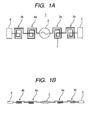
- Figs. 1(A) and (B) are schematic views illustrating an antenna device according to the embodiment.
- Fig. 1(A) is a plan view illustrating the antenna device as viewed in an opening direction of a high opening flat coil
- Fig. 1(B) is a side view illustrating the antenna device as viewed in a side direction of the high opening flat coil.
- a plurality of high opening flat coils 3a and 3b are connected in series to one side (right side in the figure) of a power supply portion 2 disposed at an antenna center, and a plurality of high opening flat coils 4a and 4b are connected in series to the other side (left side in the figure) of the power supply portion 2, thereby forming a dipole antenna.
- Radiation conductors 5 and 6 for electric field radiation by resonant current are connected to both antenna ends corresponding to electric field areas in the antenna device 1.
- Fig. 1(A) and (B) schematically show that each two high opening flat coils 3a and 3b, and 4a and 4b are connected to both sides of the power supply portion 2, but the connection number of the high opening flat coils are set to obtain necessary antenna sensitivity.
- the high opening flat coils 3a and 3b, and 4a and 4b are disposed in the vicinity of the power supply portion 2 that is the magnetic field area.
- the high opening flat coil 3a has an opening 7 where a coil center thereof is largely opened, and a conductor forms a closed area (7) as viewed in a coil opening direction in the plan view.
- a part of the conductor is disposed to overlap up and down, so that the conductor forms the closed area (7) in the plan view.
- the other high opening flat coils 3b, and 4a and 4b have the same structure.
- Fig. 2 is a perspective view illustrating the power supply portion 2, and the high opening flat coils 3a and 3b, and 4a and 4b of the antenna device 1.
- the conductor is wound four times in a rectangular shape so that the conductor forms the closed area in the plan view.
- One end 12 of the high opening flat coil 3a is connected to the power supply portion 2 through a connection portion 11.
- the one end 12 close to the power supply portion 2 is the highest position in the up and down direction, and the conductor 13 is wound once (first-winding rectangular conductor 13) in a rectangular shape at the same height from the one end 12.
- the other end of the first-winding rectangular conductor 13 wound once in the rectangular shape from the one end 12 as a starting point goes down one step slightly before the one end 12, and the second-winding rectangular conductor 14 is wound once in the rectangular shape substantially at the same position as the lower side of the first-winding rectangular conductor 13 is viewed in the plan view from that position.
- the second-winding rectangular conductor 14 has a structure in which a side opposite to the one end 12 passes through the inside by one line from the first-winding rectangular conductor 13, and the second-winding rectangular conductor 14 goes up once at the position where the next-stage high opening flat coil 3b overlaps with the connection conductor 15 to avoid interference.
- the returning side close to the one end 12 wound once in second-winding rectangular conductor 14 passes through the inside by one line from the first-winding rectangular conductor 13.
- the third-winding conductor 16 returns to the same height as the first-winding rectangular conductor 13 again, passes through the inside by one line from the first-winding and second-winding rectangular conductors 13 and 14, and is wound once in the rectangular shape.
- the fourth-winding semi-rectangular conductor 17 goes down from the position where the second-winding rectangular conductor 14 is formed, at the position close to the next-stage high opening flat coil 3b, and is connected to the end of the connection conductor 15 extending to that position.
- the rectangular conductors 13, 14, and 16, and the semi-rectangular conductor 17 which are united into one are disposed to partially overlap up and down with each other, thereby forming a large opening 7 at the center of the high opening flat coil 3a.
- the other high opening flat coil 3b is formed in the same structure.
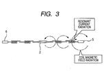
- the antenna device 1 configured as described above, radiation is performed in different modes such as resonant current radiation and magnetic field radiation as shown in Fig. 3 .
- the antenna device 1 serves as a dipole antenna.
- current and voltage are distributed on the antenna line including the plurality of high opening flat coil 3a and the like and the high opening flat coil 4a and the like, the current becomes the maximum and the voltage becomes the minimum at the power supply portion 2 disposed at the center, and the current becomes the minimum and the electric field becomes the maximum at the antenna end farthest away from the power supply portion 2.
- the resonant current radiation (radiation by resonant current) at the radiation conductors 5 and 6 (and the high opening flat coil that is away from the power supply portion 2 and is disposed at the area where magnetic field is weak) of the antenna end becomes strongest, as shown in Fig. 3 .
- the direction of the resonant current radiation is a length direction of the antenna device 1.
- a strong magnetic area is formed in the vicinity of the power supply portion 2 by the high opening flat coils 3a and 3b and the high opening flat coils 4a and 4b, and the magnetic field radiation is performed by the magnetic field generated by the high opening flat coil 3a and the like and the high opening flat coil 4a and the like as shown in Fig. 3 .
- the maximum resonant current flows when the high-frequency current supplied to the power supply portion 2 coincides with the resonant frequency of the antenna device 1. Accordingly, the magnetic field radiation at that time becomes the maximum.
- an easy-to-radiate inductance (L) having low Q is formed of the high opening flat coil 3a and the like and the high opening flat coil 4a and the like.
- the vicinity of the power supply portion 2 is the magnetic field area, where a large inductor (L) is disposed. Accordingly, there is an effect that the resonant frequency of the antenna device 1 is lowered.
- Fig. 4 is a diagram illustrating a result of antenna resonant frequency simulation for verifying the small-size effect of the antenna device 1 according to the embodiment.
- the antenna resonant frequency was about 200 MHz.
- the antenna resonant frequency was about 1000 MHz.
- the antenna resonant frequency was about 500 MHz.
- the resonant frequency of the antenna device 1 according to the embodiment is 1/2 of the case of the meandering line or less, it is possible to reduce the antenna length up to 1/2 of the case of the meandering line or less. Accordingly, it is possible to obtain the great small-size effect as compared with the case using the shortening effect of the reception signal wavelength by the relative dielectric constant of the dielectric member as described in Patent Document 1.
- Fig. 5 is a schematic view illustrating an antenna device in which resonant frequency is variable.
- the antenna device 20 shown in the same figure has the same basic configuration as the antenna device 1 shown in Fig. 1(A) and (B) .
- the same reference numerals and signs are given to the same parts, and the overlapping description thereof is omitted.
- varactor diodes 21a and 22a as variable capacitance elements are connected in series between the high opening flat coil 3a (4a) and the high opening flat coil 3b (4b), respectively.
- Cathodes of the varactor diodes 21a and 22a are connected to the ground through resistors R3 and R4, respectively.
- Tuning voltage VT is applied to anodes thereof through resistors R1 and R2.
- the other configuration is the same as the antenna device 1.
- a resonant circuit is formed of the high opening flat coil 3a and the like, the high opening flat coil 4a and the like, and the varactor diodes 21a and 22a.
- L1 denotes an inductance of the high opening flat coils 3a and 4a
- L2 denotes an inductance of the high opening flat coils 3b and 4b
- C T denotes a capacitance of the varactor diodes 21a and 22a.
- the resonant frequency Fo is shifted by varying the capacitance C T of the varactor diodes 21a and 22a.
- an antenna device 20 it is possible to reduce the size of the antenna as a radiation source for the resonant current radiation and the magnetic field radiation, and it is possible to vary the resonant frequency Fo. Therefore, it is possible to widen the band of the reception frequency and thus it is possible to receive wide-band signal such as television broadcasting.
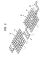
- Fig. 6 is a view illustrating a modification example of the antenna device having a changed shape of the flat coils and is an enlarged view illustrating a power supply portion and flat coils connected thereto.
- the flat coils 3a and 4a in which a line-shaped conductor 18 having a predetermined thickness is wound three times in a rectangular shape from the outside to the inside on a plane, are connected to one ends of the next flat coil 3b and 4b through the lower portions of the conductor wound in the rectangular shape at the center end of the conductor 18.
- the varactor diodes 21a and 22a are connected in series between the flat coils 3a and 4a, and the next-stage flat coils 3b and 4b, respectively.
- the conductor 18 forms a closed area in the plan view. Accordingly, radiation is performed in different modes such as resonant current radiation and magnetic field radiation. Since an easy-to-radiate inductance (L) having low Q is formed of the flat coils, a large inductance (L) is disposed in the magnetic field area. Therefore, the resonant frequency of the antenna device is lowered and thus it is possible to reduce the antenna length.
- L easy-to-radiate inductance
- L large inductance
- the antenna device a method for producing the high opening flat coil serving as the radiation source for the magnetic field radiation forming the closed area in the plan view, and the shape of the coil will be described.
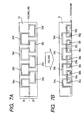
- rectangular conductive patterns 34a to 34d having opened sides on the folding line are formed in an upper half area 32 of a film substrate 31 formed of an insulating flexible film in a predetermined interval.
- Rectangular conductive patterns 35a to 35d having opened centers of sides on the folding line are formed in a lower half area 33 of the film substrate 31 at a predetermined interval to deviate from the upper conductive patterns 34a to 34d substantially by a half cycle.
- the film substrate 31 is folded along the folding line to form a plurality of flat coils, so that the closed areas 36a to 36g of the rectangular conductors are continuously formed at a predetermined interval as shown in Fig. 7(B) .
- Figs. 8 (A) and (B) show a method for producing flat coils having circular closed areas formed by conductors by way of example.
- oval conductive patterns 37a to 37c having opened straight line portions on the folding line are formed in the upper half area 32 of the film substrate 31 at a predetermined interval.
- Oval conductive patterns 38a and 38b having opened straight line portions on the folding line are formed in the lower half area 33 of the film substrate 31 at a predetermined interval to deviate from the upper conductive patterns 37a to 37c substantially by a half cycle.
- the film substrate 31 is folded along the folding line to form a plurality of flat coils, so that curved line portions of the oval conductive patterns 37a to 37c and curved line portions of the conductive patterns 38a and 38b overlap with each other and circular closed areas 39a to 39d are continuously formed at a predetermined interval as shown in Fig. 8(B) .
- Fig. 9 (A) and (B) show a method for producing flat coils having semi-circular closed areas formed by conductors by way of example.
- rectangular conductive patterns 34a to 34d having opened sides on the folding line are formed in the upper half area 32 of the film substrate 31 at a predetermined interval.
- Oval conductive patterns 41a to 41d having opened straight line portions on the folding line are formed in the lower half area 33 of the film substrate 31 at a predetermined interval to deviate from the upper conductive patterns 34a to 34d substantially by a half cycle.
- the film substrate 31 is folded along the folding line to form a plurality of flat coils, so that curved line portions of the rectangular conductive patterns 34a to 34d and curved line portions of the oval conductive patterns 41a to 41d overlap with each other and semi-circular closed areas 42a to 42g are continuously formed at a predetermined interval as shown in Fig. 9(B) .
- the dipole antenna has been described by way of example in the above description, but the invention may be applied to the monopole antenna in the same manner.
Landscapes
- Engineering & Computer Science (AREA)
- Computer Networks & Wireless Communication (AREA)
- Details Of Aerials (AREA)
- Variable-Direction Aerials And Aerial Arrays (AREA)
Abstract
Description
- The present application contains subject matter rela ted to Japanese Patent Application No.
2007-261074 - The invention relates to a dipole or monopole antenna device which is usable for a small size radio communication apparatus or the like.
- Generally, an antenna having a length larger than a wavelength has high reception sensitivity. However, when the antenna device is used as an antenna device for a cellular phone, the antenna device having the same length as the wavelength is too large in size. Accordingly, portability thereof is not good. Therefore, it is preferable to reduce the length of the antenna.
-
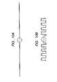
Fig. 10(A) is a schematic view illustrating a 1/2 wavelength dipole antenna. When high frequency current is supplied to the antenna, current and voltage are distributed on the line of the antenna. When the length of the antenna is integer times of the 1/2 wavelength, the antenna resonates to efficiently radiate radio wave (resonant current radiation). In the 1/2 wavelength dipole antenna, the antenna needs to have a length near the 1/2 wavelength. - To reduce the size of the antenna without changing electric field of the dipole or monopole antenna, an equivalent capacitance C or an equivalent inductance L may be raised and a resonant frequency may be lowered. However, it is not preferable that the area of the antenna is increased to raise the equivalent capacitance C. Although the inductance L may be raised without increasing the size by inserting a chip inductor, the chip inductor does not radiate. Accordingly, the total efficiency of the antenna deteriorates.
-
Fig. 10(B) is a schematic view illustrating a dipole antenna having a meandering antenna line. The length of the antenna can be reduced by about 1/8 wavelength without changing the electric field of the antenna by changing the line of the antenna to the meandering line. As the intervals of the meandering line get smaller, the length of the antenna gets smaller. However, when the intervals of the meandering line get small up to some extent, there is a limit in reducing the size by the meandering line due to the effect of the coupling capacitance between the stages. - In the dipole antenna formed of the meandering line, there has been proposed an antenna device having a length smaller than 1/8 wavelength (see Patent Document 1). The antenna device disclosed in
Patent document 1 is provided with radiating elements separately from a printed circuit board, and conductor patterns of the radiating elements are formed on a dielectric member having a larger dielectric constant than that of the printed circuit board. Accordingly, since a reception signal wavelength is more shortened by the relative dielectric constant of the dielectric member, it is possible to reduce the size of the antenna. - [Patent Document 1] Japanese Patent Application Laid-Open No.
2006-319437 - There is a limit in the shortening of the reception signal wavelength by the relative dielectric constant of the dielectric member in the antenna device disclosed in
Patent Document 1, and thus it is preferable to further reduce the size of the antenna device. - The invention has been made in consideration of such a limit, and is to provide a dipole or monopole antenna device capable of realizing great miniaturization.
- A monopole or dipole antenna device according to the invention includes a flat coil connected to a power supply point and formed of a conductor forming a closed area in a plan view in a magnetic field area in the vicinity of the power supply point, wherein magnetic field radiation is performed by the flat coil as a radiation source.
- With such a configuration, the magnetic field radiation is performed by the flat coil as the radiation source in the monopole or dipole antenna device. In addition, since an inductor (flat coil) in the magnetic file area has a high inductance, an antenna resonant frequency is lowered and thus it is possible to reduce the size of the antenna device.
- In the monopole or dipole antenna device, a plurality of flat coils may be connected. Accordingly, it is possible to lower the antenna resonant frequency by raising the inductance of the inductor (flat coil).
- In the monopole or dipole antenna device, the flat coil may be formed of a conductor provided on a film substrate.
- In the monopole or dipole antenna device, the flat coil may have conductors formed in first and second areas opposed to each other with a boundary line therebetween on the same surface of the film substrate, and the conductors overlap with each other to form a closed area in the plan view by folding the film substrate along the boundary line.
- The monopole or dipole antenna device may further includes a radiation conductor connected to the flat coil, wherein resonant current radiation is performed by the radiation conductor and magnetic field radiation is performed by the flat coil.
- With such a configuration, in the monopole or dipole antenna device, the resonant current radiation may be performed from the radiation conductor, and the magnetic field radiation may be performed from the flat coil in the vicinity of the power supply portion
- The monopole or dipole antenna device may further include a variable capacitance element connected to the flat coil in series, wherein an antenna resonant frequency is varied by applying a tuning voltage to the variable capacitance element.
- With such a configuration, since the antenna resonant frequency can be varied by applying the tuning voltage to the variable capacitance element, it is possible to widen the band of the reception frequency.
- According to the invention, it is possible to realize great miniaturization of the antenna device.
-
-
Fig. 1(A) is a schematic view illustrating an antenna device according to an embodiment and a plan view illustrating the antenna device as viewed in an opening direction of a high opening flat coil, andFig. 1(B) is a side view illustrating the antenna device as viewed in a side direction of the high opening flat coil. -
Fig. 2 is a perspective view illustrating a power supply portion and a high opening flat coil of the antenna device according to the embodiment. -
Fig. 3 is a view illustrating resonant current radiation and magnetic field radiation of the antenna device according to the embodiment. -
Fig. 4 is a diagram illustrating a result of resonant frequency simulation for verifying a small-size effect of the antenna device according to the embodiment. -
Fig. 5 is a schematic view illustrating an antenna device in which a resonant frequency is variable. -
Fig. 6 is a view illustrating a modification example of the antenna device in which the flat coil has a changed shape. -
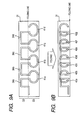
Fig. 7(A) is a plan view illustrating a state before folding in a method for producing a rectangular high opening flat coil, andFig. 7(B) is a plan view illustrating a state after folding. -
Fig. 8(A) is a plan view illustrating a state before folding in a method for producing a circular high opening flat coil, andFig. 8 (B) is a plan view illustrating a state after folding. -
Fig. 9(A) is a plan view illustrating a state before folding in a method for producing a semi-circular high opening flat coil, andFig. 9(B) is a plan view illustrating a state after folding. -
Fig. 10(A) is a schematic view illustrating a dipole antenna, andFig. 10(B) is a meandering dipole antenna. -
- 1: ANTENNA DEVICE
- 2: POWER SUPPLY PORTION
- 3a, 3b, 4a, 4b: HIGH OPENING FLAT COIL
- 5, 6: CAPACITOR
- 11: CONNECTION PORTION
- 12: ONE END OF HIGH OPENING FLAT COIL
- 13: RECTANGULAR CONDUCTOR (FIRST WINDING)
- 14: RECTANGULAR CONDUCTOR (SECOND WINDING)
- 15: CONNECTION CONDUCTOR
- 16: RECTANGULAR CONDUCTOR (THIRD WINDING)
- 17: SEMI-RECTANGULAR CONDUCTOR (FOURTH WINDING)
- 21 a, 22 a: VARACTOR DIODE
- 31: FILM SUBSTRATE
- 32: UPPER HALF AREA
- 33: LOWER HALF AREA
- 34a to 34d: CONDUCTIVE PATTERN (UPPER)
- 35a to 35d: CONDUCTIVE PATTERN (LOWER)
- Hereinafter, embodiments of an antenna device according to the invention will be described in detail with reference to the drawings.
-
Figs. 1(A) and (B) are schematic views illustrating an antenna device according to the embodiment.Fig. 1(A) is a plan view illustrating the antenna device as viewed in an opening direction of a high opening flat coil, andFig. 1(B) is a side view illustrating the antenna device as viewed in a side direction of the high opening flat coil. - In an
antenna device 1 according to the embodiment, a plurality of high openingflat coils power supply portion 2 disposed at an antenna center, and a plurality of high openingflat coils power supply portion 2, thereby forming a dipole antenna.Radiation conductors antenna device 1.Fig. 1(A) and (B) schematically show that each two high openingflat coils power supply portion 2, but the connection number of the high opening flat coils are set to obtain necessary antenna sensitivity. - The high opening
flat coils power supply portion 2 that is the magnetic field area. As shown inFig. 1(A) , the high openingflat coil 3a has anopening 7 where a coil center thereof is largely opened, and a conductor forms a closed area (7) as viewed in a coil opening direction in the plan view. As shown inFig. 1(B) , in the high openingflat coil 3a, a part of the conductor is disposed to overlap up and down, so that the conductor forms the closed area (7) in the plan view. The other high openingflat coils -
Fig. 2 is a perspective view illustrating thepower supply portion 2, and the high openingflat coils antenna device 1. In the embodiment, the conductor is wound four times in a rectangular shape so that the conductor forms the closed area in the plan view. Oneend 12 of the high openingflat coil 3a is connected to thepower supply portion 2 through aconnection portion 11. In the high openingflat coil 3a, the oneend 12 close to thepower supply portion 2 is the highest position in the up and down direction, and theconductor 13 is wound once (first-winding rectangular conductor 13) in a rectangular shape at the same height from the oneend 12. The other end of the first-windingrectangular conductor 13 wound once in the rectangular shape from the oneend 12 as a starting point goes down one step slightly before the oneend 12, and the second-windingrectangular conductor 14 is wound once in the rectangular shape substantially at the same position as the lower side of the first-windingrectangular conductor 13 is viewed in the plan view from that position. The second-windingrectangular conductor 14 has a structure in which a side opposite to the oneend 12 passes through the inside by one line from the first-windingrectangular conductor 13, and the second-windingrectangular conductor 14 goes up once at the position where the next-stage high openingflat coil 3b overlaps with theconnection conductor 15 to avoid interference. The returning side close to the oneend 12 wound once in second-windingrectangular conductor 14 passes through the inside by one line from the first-windingrectangular conductor 13. The third-windingconductor 16 returns to the same height as the first-windingrectangular conductor 13 again, passes through the inside by one line from the first-winding and second-windingrectangular conductors semi-rectangular conductor 17 goes down from the position where the second-windingrectangular conductor 14 is formed, at the position close to the next-stage high openingflat coil 3b, and is connected to the end of theconnection conductor 15 extending to that position. - As described above, the
rectangular conductors semi-rectangular conductor 17 which are united into one are disposed to partially overlap up and down with each other, thereby forming alarge opening 7 at the center of the high openingflat coil 3a. Similarly, the other high openingflat coil 3b is formed in the same structure. - In the
antenna device 1 configured as described above, radiation is performed in different modes such as resonant current radiation and magnetic field radiation as shown inFig. 3 . When high-frequency current is supplied to thepower supply portion 2, theantenna device 1 serves as a dipole antenna. In this case, current and voltage are distributed on the antenna line including the plurality of high openingflat coil 3a and the like and the high openingflat coil 4a and the like, the current becomes the maximum and the voltage becomes the minimum at thepower supply portion 2 disposed at the center, and the current becomes the minimum and the electric field becomes the maximum at the antenna end farthest away from thepower supply portion 2. When the high-frequency current supplied to thepower supply portion 2 coincides with the resonant frequency of theantenna device 1, the resonant current radiation (radiation by resonant current) at theradiation conductors 5 and 6 (and the high opening flat coil that is away from thepower supply portion 2 and is disposed at the area where magnetic field is weak) of the antenna end becomes strongest, as shown inFig. 3 . The direction of the resonant current radiation is a length direction of theantenna device 1. - A strong magnetic area is formed in the vicinity of the
power supply portion 2 by the high openingflat coils flat coils flat coil 3a and the like and the high openingflat coil 4a and the like as shown inFig. 3 . The maximum resonant current flows when the high-frequency current supplied to thepower supply portion 2 coincides with the resonant frequency of theantenna device 1. Accordingly, the magnetic field radiation at that time becomes the maximum. - In the embodiment, an easy-to-radiate inductance (L) having low Q is formed of the high opening
flat coil 3a and the like and the high openingflat coil 4a and the like. The vicinity of thepower supply portion 2 is the magnetic field area, where a large inductor (L) is disposed. Accordingly, there is an effect that the resonant frequency of theantenna device 1 is lowered. -
Fig. 4 is a diagram illustrating a result of antenna resonant frequency simulation for verifying the small-size effect of theantenna device 1 according to the embodiment. The antenna length L is set to L=150 mm. As shown in the embodiment, when the antenna line was formed of the high openingflat coil 3a and the like and the high openingflat coil 4a and the like, the antenna resonant frequency was about 200 MHz. As shown inFig. 10(A) , when the antenna line was formed of the 1/2 wavelength conductor having a straight shape, the antenna resonant frequency was about 1000 MHz. As shown inFig. 10 (B) , when the antenna line was formed of the meandering line, the antenna resonant frequency was about 500 MHz. - As described above, since the resonant frequency of the
antenna device 1 according to the embodiment is 1/2 of the case of the meandering line or less, it is possible to reduce the antenna length up to 1/2 of the case of the meandering line or less. Accordingly, it is possible to obtain the great small-size effect as compared with the case using the shortening effect of the reception signal wavelength by the relative dielectric constant of the dielectric member as described inPatent Document 1. - Next, a modification example of the antenna device in which the antenna resonant frequency is variable will be described.
-
Fig. 5 is a schematic view illustrating an antenna device in which resonant frequency is variable. Theantenna device 20 shown in the same figure has the same basic configuration as theantenna device 1 shown inFig. 1(A) and (B) . The same reference numerals and signs are given to the same parts, and the overlapping description thereof is omitted. - In an
antenna device 20,varactor diodes flat coil 3a (4a) and the high openingflat coil 3b (4b), respectively. Cathodes of thevaractor diodes antenna device 1. - In the
antenna device 20 configured as described above, a resonant circuit is formed of the high openingflat coil 3a and the like, the high openingflat coil 4a and the like, and thevaractor diodes flat coils flat coils varactor diodes antenna device 20 is represented as follows.
- CTTL is a total equivalent capacitance of the antenna, and is connected directly with a value of CT.
- Accordingly, the resonant frequency Fo is shifted by varying the capacitance CT of the
varactor diodes - According to such an
antenna device 20, it is possible to reduce the size of the antenna as a radiation source for the resonant current radiation and the magnetic field radiation, and it is possible to vary the resonant frequency Fo. Therefore, it is possible to widen the band of the reception frequency and thus it is possible to receive wide-band signal such as television broadcasting. -
Fig. 6 is a view illustrating a modification example of the antenna device having a changed shape of the flat coils and is an enlarged view illustrating a power supply portion and flat coils connected thereto. Theflat coils conductor 18 having a predetermined thickness is wound three times in a rectangular shape from the outside to the inside on a plane, are connected to one ends of the nextflat coil conductor 18. Thevaractor diodes flat coils flat coils - Even in the case of configuring the antenna device using such a flat coil, the
conductor 18 forms a closed area in the plan view. Accordingly, radiation is performed in different modes such as resonant current radiation and magnetic field radiation. Since an easy-to-radiate inductance (L) having low Q is formed of the flat coils, a large inductance (L) is disposed in the magnetic field area. Therefore, the resonant frequency of the antenna device is lowered and thus it is possible to reduce the antenna length. - In the antenna device, a method for producing the high opening flat coil serving as the radiation source for the magnetic field radiation forming the closed area in the plan view, and the shape of the coil will be described.
- As shown in
Fig. 7(A) , rectangularconductive patterns 34a to 34d having opened sides on the folding line are formed in anupper half area 32 of afilm substrate 31 formed of an insulating flexible film in a predetermined interval. Rectangularconductive patterns 35a to 35d having opened centers of sides on the folding line are formed in alower half area 33 of thefilm substrate 31 at a predetermined interval to deviate from the upperconductive patterns 34a to 34d substantially by a half cycle. - Then, the
film substrate 31 is folded along the folding line to form a plurality of flat coils, so that theclosed areas 36a to 36g of the rectangular conductors are continuously formed at a predetermined interval as shown inFig. 7(B) . -
Figs. 8 (A) and (B) show a method for producing flat coils having circular closed areas formed by conductors by way of example. As shown inFig. 8(A) , ovalconductive patterns 37a to 37c having opened straight line portions on the folding line are formed in theupper half area 32 of thefilm substrate 31 at a predetermined interval. Ovalconductive patterns lower half area 33 of thefilm substrate 31 at a predetermined interval to deviate from the upperconductive patterns 37a to 37c substantially by a half cycle. - Then, the
film substrate 31 is folded along the folding line to form a plurality of flat coils, so that curved line portions of the ovalconductive patterns 37a to 37c and curved line portions of theconductive patterns closed areas 39a to 39d are continuously formed at a predetermined interval as shown inFig. 8(B) . -
Fig. 9 (A) and (B) show a method for producing flat coils having semi-circular closed areas formed by conductors by way of example. As shown inFig. 9(A) , rectangularconductive patterns 34a to 34d having opened sides on the folding line are formed in theupper half area 32 of thefilm substrate 31 at a predetermined interval. Ovalconductive patterns 41a to 41d having opened straight line portions on the folding line are formed in thelower half area 33 of thefilm substrate 31 at a predetermined interval to deviate from the upperconductive patterns 34a to 34d substantially by a half cycle. - Then, the
film substrate 31 is folded along the folding line to form a plurality of flat coils, so that curved line portions of the rectangularconductive patterns 34a to 34d and curved line portions of the ovalconductive patterns 41a to 41d overlap with each other and semi-circularclosed areas 42a to 42g are continuously formed at a predetermined interval as shown inFig. 9(B) . - The dipole antenna has been described by way of example in the above description, but the invention may be applied to the monopole antenna in the same manner.
Claims (6)
- A monopole or dipole antenna device comprising a flat coil connected to a power supply point and formed of a conductor forming a closed area in a plan view in a magnetic field area in the vicinity of the power supply point, wherein magnetic field radiation is performed by the flat coil as a radiation source.
- The monopole or dipole antenna device according to Claim 1, wherein a plurality of the flat coils are connected.
- The monopole or dipole antenna device according to Claim 1 or 2, wherein the flat coil is formed of a conductor provided on a film substrate.
- The monopole or dipole antenna device according to any one of Claims 1 to 3, wherein the flat coil has conductors formed in first and second areas opposed to each other with a boundary line therebetween on the same surface of the film substrate, and the conductors overlap with each other to form a closed area in the plan view by folding the film substrate along the boundary line.
- The monopole or dipole antenna device according to any one of Claims 1 to 4, further comprising a radiation conductor connected to the flat coil, wherein resonant current radiation is performed by the radiation conductor and magnetic field radiation is performed by the flat coil.
- The monopole or dipole antenna device according to any one of Claims 1 to 5, further comprising a variable capacitance element connected to the flat coil in series, wherein an antenna resonant frequency is varied by applying a tuning voltage to the variable capacitance element.
Applications Claiming Priority (1)
| Application Number | Priority Date | Filing Date | Title |
|---|---|---|---|
| JP2007261074A JP4790684B2 (en) | 2007-10-04 | 2007-10-04 | Antenna device |
Publications (2)
| Publication Number | Publication Date |
|---|---|
| EP2045876A2 true EP2045876A2 (en) | 2009-04-08 |
| EP2045876A3 EP2045876A3 (en) | 2014-07-16 |
Family
ID=40298202
Family Applications (1)
| Application Number | Title | Priority Date | Filing Date |
|---|---|---|---|
| EP08016951.9A Withdrawn EP2045876A3 (en) | 2007-10-04 | 2008-09-25 | Antenna device |
Country Status (2)
| Country | Link |
|---|---|
| EP (1) | EP2045876A3 (en) |
| JP (1) | JP4790684B2 (en) |
Cited By (3)
| Publication number | Priority date | Publication date | Assignee | Title |
|---|---|---|---|---|
| EP2755279A1 (en) * | 2013-01-11 | 2014-07-16 | Roke Manor Research Limited | A dipole antenna |
| CN113889763A (en) * | 2021-11-08 | 2022-01-04 | 山东炎一智能科技有限公司 | FPC antenna and electronic device |
| CN114006153A (en) * | 2021-12-01 | 2022-02-01 | 山东炎一智能科技有限公司 | FPC antenna and mobile device |
Families Citing this family (2)
| Publication number | Priority date | Publication date | Assignee | Title |
|---|---|---|---|---|
| JP7170319B2 (en) * | 2019-02-21 | 2022-11-14 | 国立大学法人京都工芸繊維大学 | antenna device |
| JP7574665B2 (en) * | 2021-01-26 | 2024-10-29 | Toppanホールディングス株式会社 | Antenna and contactless data transmitter and receiver |
Citations (2)
| Publication number | Priority date | Publication date | Assignee | Title |
|---|---|---|---|---|
| JP2006319437A (en) | 2005-05-10 | 2006-11-24 | Sharp Corp | antenna |
| JP2007261074A (en) | 2006-03-28 | 2007-10-11 | Nippon Synthetic Chem Ind Co Ltd:The | Multilayer stretched film |
Family Cites Families (8)
| Publication number | Priority date | Publication date | Assignee | Title |
|---|---|---|---|---|
| JPS59140508U (en) * | 1983-03-11 | 1984-09-19 | 日本アンテナ株式会社 | Whip antenna for communication |
| JPH0750843B2 (en) * | 1990-11-19 | 1995-05-31 | 富士通テン株式会社 | antenna |
| JPH04103711U (en) * | 1991-01-24 | 1992-09-07 | 松下電器産業株式会社 | small antenna |
| JPH1146109A (en) * | 1997-07-25 | 1999-02-16 | Denso Corp | antenna |
| JP2001143029A (en) * | 1999-11-11 | 2001-05-25 | Sony Corp | IC card manufacturing method |
| US6630906B2 (en) * | 2000-07-24 | 2003-10-07 | The Furukawa Electric Co., Ltd. | Chip antenna and manufacturing method of the same |
| JP2002319813A (en) * | 2000-07-24 | 2002-10-31 | Furukawa Electric Co Ltd:The | Chip antenna and manufacturing method thereof |
| JP2004096341A (en) * | 2002-08-30 | 2004-03-25 | Fujitsu Ltd | Antenna device including inverted F-type antenna with variable resonance frequency |
-
2007
- 2007-10-04 JP JP2007261074A patent/JP4790684B2/en not_active Expired - Fee Related
-
2008
- 2008-09-25 EP EP08016951.9A patent/EP2045876A3/en not_active Withdrawn
Patent Citations (2)
| Publication number | Priority date | Publication date | Assignee | Title |
|---|---|---|---|---|
| JP2006319437A (en) | 2005-05-10 | 2006-11-24 | Sharp Corp | antenna |
| JP2007261074A (en) | 2006-03-28 | 2007-10-11 | Nippon Synthetic Chem Ind Co Ltd:The | Multilayer stretched film |
Cited By (4)
| Publication number | Priority date | Publication date | Assignee | Title |
|---|---|---|---|---|
| EP2755279A1 (en) * | 2013-01-11 | 2014-07-16 | Roke Manor Research Limited | A dipole antenna |
| GB2510981A (en) * | 2013-01-11 | 2014-08-20 | Roke Manor Research | A dipole antenna |
| CN113889763A (en) * | 2021-11-08 | 2022-01-04 | 山东炎一智能科技有限公司 | FPC antenna and electronic device |
| CN114006153A (en) * | 2021-12-01 | 2022-02-01 | 山东炎一智能科技有限公司 | FPC antenna and mobile device |
Also Published As
| Publication number | Publication date |
|---|---|
| JP4790684B2 (en) | 2011-10-12 |
| EP2045876A3 (en) | 2014-07-16 |
| JP2009094631A (en) | 2009-04-30 |
Similar Documents
| Publication | Publication Date | Title |
|---|---|---|
| CN109716583B (en) | Antenna devices and electronic equipment | |
| CN102204112B (en) | Radio communication device | |
| CN207765315U (en) | Magnetic field coupled element, antenna assembly and electronic equipment | |
| US9059520B2 (en) | Wireless communication device and communication terminal apparatus | |
| CN105075005B (en) | Save space-efficient multiband antenna | |
| CN101461092B (en) | Antenna device | |
| JP5834987B2 (en) | ANTENNA DEVICE AND WIRELESS COMMUNICATION DEVICE | |
| JP2004336250A (en) | Antenna matching circuit, and mobile communication apparatus and dielectric antenna having the same | |
| US7170456B2 (en) | Dielectric chip antenna structure | |
| EP2139065A1 (en) | Antenna device | |
| CN212676477U (en) | Antenna device and communication terminal device | |
| JP4790684B2 (en) | Antenna device | |
| JP2013530623A (en) | Antenna with planar conductive element | |
| JP4073789B2 (en) | Dielectric antenna and mobile communication device incorporating the same | |
| US7034750B2 (en) | Antenna mounting printed-circuit board | |
| US11450969B1 (en) | Compact slot-based antenna design for narrow band internet of things applications | |
| CN101432928A (en) | Antenna structure and wireless communication device using same | |
| JP2004186731A (en) | Chip antenna and wireless communication apparatus using the same | |
| JP3842963B2 (en) | Antenna element | |
| JP6897900B1 (en) | Antenna device and electronic equipment | |
| JP2013172281A (en) | Antenna device and radio communication device | |
| WO2023032511A1 (en) | Antenna device and communication terminal device | |
| JP2010136114A (en) | Radio communication device | |
| JP2009296270A (en) | Antenna device | |
| JP2009296483A (en) | Antenna device |
Legal Events
| Date | Code | Title | Description |
|---|---|---|---|
| PUAI | Public reference made under article 153(3) epc to a published international application that has entered the european phase |
Free format text: ORIGINAL CODE: 0009012 |
|
| AK | Designated contracting states |
Kind code of ref document: A2 Designated state(s): AT BE BG CH CY CZ DE DK EE ES FI FR GB GR HR HU IE IS IT LI LT LU LV MC MT NL NO PL PT RO SE SI SK TR |
|
| AX | Request for extension of the european patent |
Extension state: AL BA MK RS |
|
| RIC1 | Information provided on ipc code assigned before grant |
Ipc: H01Q 21/29 20060101ALI20140131BHEP Ipc: H01Q 9/16 20060101ALI20140131BHEP Ipc: H01Q 1/36 20060101ALI20140131BHEP Ipc: H01Q 1/38 20060101AFI20140131BHEP Ipc: H01Q 1/24 20060101ALI20140131BHEP Ipc: H01Q 9/28 20060101ALI20140131BHEP |
|
| PUAL | Search report despatched |
Free format text: ORIGINAL CODE: 0009013 |
|
| AK | Designated contracting states |
Kind code of ref document: A3 Designated state(s): AT BE BG CH CY CZ DE DK EE ES FI FR GB GR HR HU IE IS IT LI LT LU LV MC MT NL NO PL PT RO SE SI SK TR |
|
| AX | Request for extension of the european patent |
Extension state: AL BA MK RS |
|
| RIC1 | Information provided on ipc code assigned before grant |
Ipc: H01Q 1/38 20060101AFI20140612BHEP Ipc: H01Q 9/28 20060101ALI20140612BHEP Ipc: H01Q 1/24 20060101ALI20140612BHEP Ipc: H01Q 21/29 20060101ALI20140612BHEP Ipc: H01Q 1/36 20060101ALI20140612BHEP Ipc: H01Q 9/16 20060101ALI20140612BHEP |
|
| AKY | No designation fees paid | ||
| AXX | Extension fees paid |
Extension state: BA Extension state: RS Extension state: MK Extension state: AL |
|
| REG | Reference to a national code |
Ref country code: DE Ref legal event code: R108 |
|
| REG | Reference to a national code |
Ref country code: DE Ref legal event code: R108 Effective date: 20150325 |
|
| STAA | Information on the status of an ep patent application or granted ep patent |
Free format text: STATUS: THE APPLICATION IS DEEMED TO BE WITHDRAWN |
|
| 18D | Application deemed to be withdrawn |
Effective date: 20150117 |