EP2045519A1 - Power supply board, board connector, lighting apparatus, display apparatus and television receiver - Google Patents
Power supply board, board connector, lighting apparatus, display apparatus and television receiver Download PDFInfo
- Publication number
- EP2045519A1 EP2045519A1 EP07744066A EP07744066A EP2045519A1 EP 2045519 A1 EP2045519 A1 EP 2045519A1 EP 07744066 A EP07744066 A EP 07744066A EP 07744066 A EP07744066 A EP 07744066A EP 2045519 A1 EP2045519 A1 EP 2045519A1
- Authority
- EP
- European Patent Office
- Prior art keywords
- board
- output terminal
- circuit board
- chassis
- relay
- Prior art date
- Legal status (The legal status is an assumption and is not a legal conclusion. Google has not performed a legal analysis and makes no representation as to the accuracy of the status listed.)
- Granted
Links
Images
















Classifications
-
- G—PHYSICS
- G02—OPTICS
- G02F—OPTICAL DEVICES OR ARRANGEMENTS FOR THE CONTROL OF LIGHT BY MODIFICATION OF THE OPTICAL PROPERTIES OF THE MEDIA OF THE ELEMENTS INVOLVED THEREIN; NON-LINEAR OPTICS; FREQUENCY-CHANGING OF LIGHT; OPTICAL LOGIC ELEMENTS; OPTICAL ANALOGUE/DIGITAL CONVERTERS
- G02F1/00—Devices or arrangements for the control of the intensity, colour, phase, polarisation or direction of light arriving from an independent light source, e.g. switching, gating or modulating; Non-linear optics
- G02F1/01—Devices or arrangements for the control of the intensity, colour, phase, polarisation or direction of light arriving from an independent light source, e.g. switching, gating or modulating; Non-linear optics for the control of the intensity, phase, polarisation or colour
- G02F1/13—Devices or arrangements for the control of the intensity, colour, phase, polarisation or direction of light arriving from an independent light source, e.g. switching, gating or modulating; Non-linear optics for the control of the intensity, phase, polarisation or colour based on liquid crystals, e.g. single liquid crystal display cells
- G02F1/133—Constructional arrangements; Operation of liquid crystal cells; Circuit arrangements
- G02F1/1333—Constructional arrangements; Manufacturing methods
- G02F1/1335—Structural association of cells with optical devices, e.g. polarisers or reflectors
-
- H—ELECTRICITY
- H01—ELECTRIC ELEMENTS
- H01R—ELECTRICALLY-CONDUCTIVE CONNECTIONS; STRUCTURAL ASSOCIATIONS OF A PLURALITY OF MUTUALLY-INSULATED ELECTRICAL CONNECTING ELEMENTS; COUPLING DEVICES; CURRENT COLLECTORS
- H01R33/00—Coupling devices specially adapted for supporting apparatus and having one part acting as a holder providing support and electrical connection via a counterpart which is structurally associated with the apparatus, e.g. lamp holders; Separate parts thereof
- H01R33/94—Holders formed as intermediate parts for linking a counter-part to a coupling part
-
- G—PHYSICS
- G02—OPTICS
- G02F—OPTICAL DEVICES OR ARRANGEMENTS FOR THE CONTROL OF LIGHT BY MODIFICATION OF THE OPTICAL PROPERTIES OF THE MEDIA OF THE ELEMENTS INVOLVED THEREIN; NON-LINEAR OPTICS; FREQUENCY-CHANGING OF LIGHT; OPTICAL LOGIC ELEMENTS; OPTICAL ANALOGUE/DIGITAL CONVERTERS
- G02F1/00—Devices or arrangements for the control of the intensity, colour, phase, polarisation or direction of light arriving from an independent light source, e.g. switching, gating or modulating; Non-linear optics
- G02F1/01—Devices or arrangements for the control of the intensity, colour, phase, polarisation or direction of light arriving from an independent light source, e.g. switching, gating or modulating; Non-linear optics for the control of the intensity, phase, polarisation or colour
- G02F1/13—Devices or arrangements for the control of the intensity, colour, phase, polarisation or direction of light arriving from an independent light source, e.g. switching, gating or modulating; Non-linear optics for the control of the intensity, phase, polarisation or colour based on liquid crystals, e.g. single liquid crystal display cells
- G02F1/133—Constructional arrangements; Operation of liquid crystal cells; Circuit arrangements
- G02F1/1333—Constructional arrangements; Manufacturing methods
- G02F1/1335—Structural association of cells with optical devices, e.g. polarisers or reflectors
- G02F1/1336—Illuminating devices
- G02F1/133602—Direct backlight
- G02F1/133604—Direct backlight with lamps
-
- H—ELECTRICITY
- H01—ELECTRIC ELEMENTS
- H01R—ELECTRICALLY-CONDUCTIVE CONNECTIONS; STRUCTURAL ASSOCIATIONS OF A PLURALITY OF MUTUALLY-INSULATED ELECTRICAL CONNECTING ELEMENTS; COUPLING DEVICES; CURRENT COLLECTORS
- H01R12/00—Structural associations of a plurality of mutually-insulated electrical connecting elements, specially adapted for printed circuits, e.g. printed circuit boards [PCB], flat or ribbon cables, or like generally planar structures, e.g. terminal strips, terminal blocks; Coupling devices specially adapted for printed circuits, flat or ribbon cables, or like generally planar structures; Terminals specially adapted for contact with, or insertion into, printed circuits, flat or ribbon cables, or like generally planar structures
- H01R12/50—Fixed connections
- H01R12/51—Fixed connections for rigid printed circuits or like structures
-
- H—ELECTRICITY
- H01—ELECTRIC ELEMENTS
- H01R—ELECTRICALLY-CONDUCTIVE CONNECTIONS; STRUCTURAL ASSOCIATIONS OF A PLURALITY OF MUTUALLY-INSULATED ELECTRICAL CONNECTING ELEMENTS; COUPLING DEVICES; CURRENT COLLECTORS
- H01R12/00—Structural associations of a plurality of mutually-insulated electrical connecting elements, specially adapted for printed circuits, e.g. printed circuit boards [PCB], flat or ribbon cables, or like generally planar structures, e.g. terminal strips, terminal blocks; Coupling devices specially adapted for printed circuits, flat or ribbon cables, or like generally planar structures; Terminals specially adapted for contact with, or insertion into, printed circuits, flat or ribbon cables, or like generally planar structures
- H01R12/50—Fixed connections
- H01R12/51—Fixed connections for rigid printed circuits or like structures
- H01R12/55—Fixed connections for rigid printed circuits or like structures characterised by the terminals
-
- H—ELECTRICITY
- H01—ELECTRIC ELEMENTS
- H01R—ELECTRICALLY-CONDUCTIVE CONNECTIONS; STRUCTURAL ASSOCIATIONS OF A PLURALITY OF MUTUALLY-INSULATED ELECTRICAL CONNECTING ELEMENTS; COUPLING DEVICES; CURRENT COLLECTORS
- H01R33/00—Coupling devices specially adapted for supporting apparatus and having one part acting as a holder providing support and electrical connection via a counterpart which is structurally associated with the apparatus, e.g. lamp holders; Separate parts thereof
- H01R33/02—Single-pole devices, e.g. holder for supporting one end of a tubular incandescent or neon lamp
-
- H—ELECTRICITY
- H01—ELECTRIC ELEMENTS
- H01R—ELECTRICALLY-CONDUCTIVE CONNECTIONS; STRUCTURAL ASSOCIATIONS OF A PLURALITY OF MUTUALLY-INSULATED ELECTRICAL CONNECTING ELEMENTS; COUPLING DEVICES; CURRENT COLLECTORS
- H01R33/00—Coupling devices specially adapted for supporting apparatus and having one part acting as a holder providing support and electrical connection via a counterpart which is structurally associated with the apparatus, e.g. lamp holders; Separate parts thereof
- H01R33/74—Devices having four or more poles, e.g. holders for compact fluorescent lamps
- H01R33/76—Holders with sockets, clips, or analogous contacts adapted for axially-sliding engagement with parallely-arranged pins, blades, or analogous contacts on counterpart, e.g. electronic tube socket
- H01R33/7607—Holders with sockets, clips, or analogous contacts adapted for axially-sliding engagement with parallely-arranged pins, blades, or analogous contacts on counterpart, e.g. electronic tube socket the parallel terminal pins having a circular disposition
- H01R33/7635—Holders with sockets, clips, or analogous contacts adapted for axially-sliding engagement with parallely-arranged pins, blades, or analogous contacts on counterpart, e.g. electronic tube socket the parallel terminal pins having a circular disposition the terminals being collectively connected, e.g. to a PCB
- H01R33/7642—Holders with sockets, clips, or analogous contacts adapted for axially-sliding engagement with parallely-arranged pins, blades, or analogous contacts on counterpart, e.g. electronic tube socket the parallel terminal pins having a circular disposition the terminals being collectively connected, e.g. to a PCB socket snap fastened in an opening of a PCB
-
- G—PHYSICS
- G02—OPTICS
- G02F—OPTICAL DEVICES OR ARRANGEMENTS FOR THE CONTROL OF LIGHT BY MODIFICATION OF THE OPTICAL PROPERTIES OF THE MEDIA OF THE ELEMENTS INVOLVED THEREIN; NON-LINEAR OPTICS; FREQUENCY-CHANGING OF LIGHT; OPTICAL LOGIC ELEMENTS; OPTICAL ANALOGUE/DIGITAL CONVERTERS
- G02F1/00—Devices or arrangements for the control of the intensity, colour, phase, polarisation or direction of light arriving from an independent light source, e.g. switching, gating or modulating; Non-linear optics
- G02F1/01—Devices or arrangements for the control of the intensity, colour, phase, polarisation or direction of light arriving from an independent light source, e.g. switching, gating or modulating; Non-linear optics for the control of the intensity, phase, polarisation or colour
- G02F1/13—Devices or arrangements for the control of the intensity, colour, phase, polarisation or direction of light arriving from an independent light source, e.g. switching, gating or modulating; Non-linear optics for the control of the intensity, phase, polarisation or colour based on liquid crystals, e.g. single liquid crystal display cells
- G02F1/133—Constructional arrangements; Operation of liquid crystal cells; Circuit arrangements
- G02F1/1333—Constructional arrangements; Manufacturing methods
- G02F1/1335—Structural association of cells with optical devices, e.g. polarisers or reflectors
- G02F1/1336—Illuminating devices
- G02F1/133602—Direct backlight
- G02F1/133608—Direct backlight including particular frames or supporting means
-
- G—PHYSICS
- G02—OPTICS
- G02F—OPTICAL DEVICES OR ARRANGEMENTS FOR THE CONTROL OF LIGHT BY MODIFICATION OF THE OPTICAL PROPERTIES OF THE MEDIA OF THE ELEMENTS INVOLVED THEREIN; NON-LINEAR OPTICS; FREQUENCY-CHANGING OF LIGHT; OPTICAL LOGIC ELEMENTS; OPTICAL ANALOGUE/DIGITAL CONVERTERS
- G02F1/00—Devices or arrangements for the control of the intensity, colour, phase, polarisation or direction of light arriving from an independent light source, e.g. switching, gating or modulating; Non-linear optics
- G02F1/01—Devices or arrangements for the control of the intensity, colour, phase, polarisation or direction of light arriving from an independent light source, e.g. switching, gating or modulating; Non-linear optics for the control of the intensity, phase, polarisation or colour
- G02F1/13—Devices or arrangements for the control of the intensity, colour, phase, polarisation or direction of light arriving from an independent light source, e.g. switching, gating or modulating; Non-linear optics for the control of the intensity, phase, polarisation or colour based on liquid crystals, e.g. single liquid crystal display cells
- G02F1/133—Constructional arrangements; Operation of liquid crystal cells; Circuit arrangements
- G02F1/1333—Constructional arrangements; Manufacturing methods
- G02F1/1335—Structural association of cells with optical devices, e.g. polarisers or reflectors
- G02F1/1336—Illuminating devices
- G02F1/133602—Direct backlight
- G02F1/133612—Electrical details
Definitions
- the present invention relates to a power board, an on-board connector, a lighting device, a display device and a television receiver.
- the lighting device has a construction, in which relay terminals are mounted into through holes formed on a chassis that has a substantially flat plate-like shape and functions as a reflector plate.
- An electrode part of a discharge tube arranged on the front side of the chassis and a power board arranged on the back side of the chassis are connected to each relay connector, so that the discharge tube can receive the power supply from the power board via the relay terminal.
- a power board according to the present invention which is to be mounted to the back side of a chassis having substantially a plate-like shape, includes a circuit board capable of being arranged substantially parallel to the chassis, and an on-board connector mounted to the circuit board.
- the output terminal of the on-board connector can be connected to a relay terminal provided on the chassis, so that power is supplied to a discharge tube arranged on the front side of the chassis.
- a fitting hole is formed through the circuit board so as to extend from the front surface to the back surface thereof.
- the on-board connector is mounted to the back surface of the circuit board, and is positioned to correspond to the fitting hole.
- the relay terminal and the output terminal can be connected to each other, while one or both thereof penetrate the circuit board through the fitting hole.
- the fitting hole is thus formed as a through hole on the circuit board, and thereby the on-board connector, provided for connection to the relay terminal on the chassis, can be arranged on the back surface of the circuit board on the opposite side of the chassis.
- electronic components free from restriction of the positional relationship with the chassis can be mounted on the back surface of the circuit board, as is the on-board connector.
- the power board connected to the relay terminal on the chassis can be thus achieved as a single-sided power board in which the back surface on the opposite side of the chassis is provided as the single mounting surface.
- the on-board connector can include a housing made of an insulating material, so that the output terminal is at least partly held in the housing.
- the output terminal is at least partly held in the housing, and therefore the part held in the housing can be prevented from interference with foreign substances.
- an engaging recess having an opening corresponding to the fitting hole can be formed on the housing, so that the output terminal is arranged in the engaging recess.
- the relay terminal can be inserted into the engaging recess so as to be connected to the output terminal therewithin. Thereby, the connection between the terminals can be prevented from interference with foreign substances.
- a positioning portion which can lock the output terminal so that displacement of the output terminal along the inside surface of the engaging recess is restricted, may be provided on the inside surface.
- the displacement of the output terminal is restricted by the positioning portion, and therefore the flexural rigidity of the output terminal is not required to be increased for displacement prevention.
- the reduced flexural rigidity of the output terminal thus provided, results in reduction of the frictional resistance developed when the relay terminal is connected to the output terminal.
- the operational efficiency at the time of connection can be improved.
- the output terminal can include a proximal portion fixed to the housing, a flexible portion extending from the proximal portion and being capable of elastic deflection, and a connecting part extending from the flexible portion and having substantially a U-shape capable of elastically pinching the relay terminal.
- the connecting part may include two strip portions, so that a free-end-side strip portion of the two strip portions on the opposite side of the flexible portion can have contact with the relay terminal.
- the whole connecting part moves to the flexible portion side, together with the relay terminal.
- the connection between the relay terminal and the free-end-side strip portion can be maintained. If the relay terminal moves or displaces from the output terminal to the free end side or to the opposite side of the flexible portion, the free-end-side strip portion of the connecting part is pushed by the relay terminal into movement. Then, the connection between the relay terminal and the free-end-side strip portion can be also maintained.
- the output terminal can include a connecting part that is elongated in a direction substantially perpendicular to the array direction of the on-board connectors.
- the connecting part can have contact with the relay terminal that forms a plate-like shape having a width larger than that of the connecting part and to be arranged parallel to the array direction of the on-board connectors.
- the output terminals of the on-board connectors may displace in the array direction from the relay terminals due to some reason such as the difference in thermal expansion rate between the circuit board as a mounting base for the on-board connectors and the chassis as a mounting base for the relay terminals.
- the connecting part is provided on the output terminal so as to be elongated in a direction substantially perpendicular to the array direction of the on-board connectors, while the relay terminal having a plate-like shape, wider than the connecting part and to be arranged parallel to the array direction of the on-board connectors, is provided so as to be capable of contact with the connecting part.
- the relay terminal is set to be large in width along the array direction, and therefore the connection between the relay terminal and the connecting part can be maintained even if the relay terminal displaces in the array direction from the output terminal.
- the on-board connector can be arranged along an edge portion of the circuit board.
- the output terminal may be arranged on an area of the housing on the opposite side of the edge portion, so that a sectional arrangement is provided.
- the output terminal is arranged on the area of the housing on the opposite side of the edge portion of the circuit board, resulting in sectional arrangement. Consequently, a low-voltage area is left on a portion of the on-board connector located in proximity to the edge portion of the circuit board.
- an on-board connector which is to be mounted to a circuit board in order to form a power board.
- the power board can be mounted to the back side of a chassis having substantially a plate-like shape, so that the circuit board is arranged substantially parallel to the chassis.
- the on-board connector includes an output terminal that can be connected to a relay terminal provided on the chassis so that power is supplied to a discharge tube arranged on the front side of the chassis.
- the on-board connector can be mounted to the back surface of the circuit board, and be positioned to correspond to a fitting hole that is formed through the circuit board so as to extend from the front surface to the back surface thereof.
- the relay terminal and the output terminal can be connected to each other, while one or both thereof penetrate the circuit board through the fitting hole.
- the fitting hole is thus formed as a through hole on the circuit board, and thereby the on-board connector, provided for connection to the relay terminal on the chassis, can be arranged on the back surface of the circuit board on the opposite side of the chassis.
- electronic components free from restriction of the positional relationship with the chassis can be mounted on the back surface of the circuit board, as is the on-board connector.
- the power board connected to the relay terminal on the chassis can be thus achieved as a single-sided power board in which the back surface on the opposite side of the chassis is provided as the single mounting surface.
- the on-board connector can further include a housing made of an insulating material, so that the output terminal is at least partly held in the housing.
- the output terminal is at least partly held in the housing, and therefore the part held in the housing can be prevented from interference with foreign substances.
- an engaging recess having an opening capable of being arranged to correspond to the fitting hole, can be formed on the housing, so that the output terminal is arranged in the engaging recess.
- the relay terminal can be inserted into the engaging recess so as to be connected to the output terminal therewithin. Thereby, the connection between the terminals can be prevented from interference with foreign substances.
- a positioning portion which can lock the output terminal so that displacement of the output terminal along the inside surface of the engaging recess is restricted, may be provided on the inside surface.
- the displacement of the output terminal is restricted by the positioning portion, and therefore the flexural rigidity of the output terminal is not required to be increased for displacement prevention.
- the reduced flexural rigidity of the output terminal thus provided, results in reduction of the frictional resistance developed when the relay terminal is connected to the output terminal.
- the operational efficiency at the time of connection can be improved.
- the output terminal can include a proximal portion fixed to the housing, a flexible portion extending from the proximal portion and being capable of elastic deflection, and a connecting part extending from the flexible portion and having substantially a U-shape capable of elastically pinching the relay terminal.
- the connecting part may include two strip portions, so that a free-end-side strip portion of the two strip portions on the opposite side of the flexible portion can have contact with the relay terminal.
- the whole connecting part moves to the flexible portion side, together with the relay terminal.
- the connection between the relay terminal and the free-end-side strip portion can be maintained. If the relay terminal moves or displaces from the output terminal to the free end side or to the opposite side of the flexible portion, the free-end-side strip portion of the connecting part is pushed by the relay terminal into movement. Then, the connection between the relay terminal and the free-end-side strip portion can be also maintained.
- the output terminal can include a connecting part that is elongated in a direction substantially perpendicular to the array direction.
- the connecting part can have contact with the relay terminal that forms a plate-like shape having a width larger than that of the connecting part and to be arranged parallel to the array direction.
- the output terminals of the on-board connectors may displace in the array direction from the relay terminals due to some reason such as the difference in thermal expansion rate between the circuit board as a mounting base for the on-board connectors and the chassis as a mounting base for the relay terminals.
- the connecting part is provided on the output terminal so as to be elongated in a direction substantially perpendicular to the array direction of the on-board connectors, while the relay terminal having a plate-like shape, wider than the connecting part and to be arranged parallel to the array direction of the on-board connectors, is provided so as to be capable of contact with the connecting part.
- the relay terminal is set to be large in width along the array direction, and therefore the connection between the relay terminal and the connecting part can be maintained even if the relay terminal displaces in the array direction from the output terminal.
- the housing can be arranged along an edge portion of the circuit board.
- the output terminal may be arranged on an area of the housing that can be positioned on the opposite side of the edge portion, so that a sectional arrangement is provided.
- the output terminal is arranged on the area of the housing that can be positioned on the opposite side of the edge portion of the circuit board, resulting in sectional arrangement. Consequently, a low-voltage area is left on a portion of the on-board connector located in proximity to the edge portion of the circuit board.
- a lighting device includes a power board according to the present invention described above, a chassis and a discharge tube.
- a display device includes a lighting device according to the present invention described above, and a display panel arranged on the front side of the lighting device.
- a television receiver according to the present invention includes a display device according to the present invention described above.
- FIGS. 1 to 16 An embodiment 1 according to the present invention will be hereinafter explained with reference to FIGS. 1 to 16 .
- a display device D shown in FIG. 16 is a so-called liquid crystal display device including a display panel 11 and a lighting device 10 as shown in FIG. 1 , which forms a horizontally-elongated rectangular shape as a whole.
- the display panel 11 is disposed on the front side of the lighting device 10, so that the lighting device 10 as a backlight can illuminate the display panel 11 from the back side.
- the display device D can be applied to a television receiver.
- the television receiver includes the display device D, and front and back cabinets Ca and Cb capable of holding the display device D therebetween. Further included are a power source P other than a power board 16 described below, a tuner T and a stand S.
- the display panel 11 has a well-known construction, in which liquid crystal as a material with an optical property that changes with applied voltage is disposed in the gap between a transparent TFT substrate and a transparent CF substrate.
- TFTs Thin Film Transistors
- a color filter on which color sections of three primary colors, i.e., Red (R), Green (G) and Blue (B), are arranged in a matrix, is provided on the CF substrate.
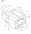
- each relay connector 14 includes a holder 20 made of synthetic resin, and a metallic relay terminal 30 housed in the holder 20.
- a pair of upper and lower elastic retaining parts 25 and a pair of right and left engaging surfaces 26 are formed on the outer surface of the holder 20.
- the holder 20 is inserted into the mounting hole 13H from the front side of the chassis 13, and is fixed to the chassis 13 due to the engaging surfaces 26 in abutting contact with the opening edge of the mounting hole 13H on the front surface of the chassis 13 and due to the retaining protrusions of the elastic retaining parts 25 being locked by the opening edge of the mounting hole 13H on the back surface of the chassis 13.
- the front end portion of the holder 20 projects to the front side of the chassis 13, while the back end portion of the holder 20 projects to the back side of the chassis 13.
- a container room 23 is formed in the projecting portion of the holder 20 on the front side of the chassis 13, by removing the front surface and one lateral surface thereof.
- a plate-like wall portion 27 is formed on the projecting portion of the holder 20 on the back side of the chassis 13.
- the relay terminal 30 is disposed in the holder 20.
- the relay terminal 30, which can be formed by bending a metallic plate that is formed into a predetermined shape by punching, includes a tube connecting portion 31 having a pair of upper and lower elastic nipping parts 32 formed of plates having a substantially circular arc shape, and further includes a plate-like board connecting portion 33 projecting to the back side.
- the tube connecting portion 31 is disposed in the container room 23, while the board connecting portion 33 is arranged along the wall portion 27.
- each discharge tube 15 is formed of a cold cathode fluorescent tube that includes a generally elongated straight glass tube 40 having a circular cross section, elongated outer leads 42 which have a circular cross section and project linearly from the respective ends of the glass tube 40 and coaxially with the glass tube 40, and further includes ferrules 50 attached to the respective end portions of the glass tube 40.
- Each ferrule 50 which can be formed by bending or hammering a metallic (e.g., copper alloy) plate that is formed into a predetermined shape by punching, includes a body 51 and a conductive part 57.
- the body 51 generally forms a cylindrical shape, which is attached on the outer circumference of the glass tube 40.
- the conductive part 57 extends from the end edge of the body 51 so as to have elastic contact with the outer periphery of the outer lead 42, and is fixed by welding.
- the discharge tube 15 is mounted to the chassis 13, so that the end portions thereof are fitted into the container rooms 23 of the holders 20 while tube connecting portions 31 have elastic contact with the outer circumferences of the bodies 51 of the ferrules 50.
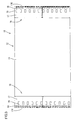
- each power board 16 includes a circuit board 17 having a circuit formed on its back surface (i.e., the surface on the opposite side of the chassis 13), electronic components 19 mounted on the back surface of the circuit board 17, and a plurality of on-board connectors 18 mounted on the back surface of the circuit board 17.
- the circuit board 17 has a vertically-elongated rectangular shape as a whole, and is formed using a phenolic paper-base copper-clad laminated board (known as a phenolic paper).
- a plurality of fitting holes 17H having a vertically-elongated rectangular shape are formed through the circuit board 17 so as to extend from the front side to the back side.
- the plurality of fitting holes 17H are arranged vertically along the lateral edge portion 17E (or side edge portion) of the circuit board 17 so as to correspond to the above-described relay terminals 30 (or relay connectors 14). Further, a plurality of positioning holes 17a are formed through the circuit board 17 so as to extend from the front side to the back side. The positioning holes 17a are arranged between the fitting holes 17H and the side edge of the circuit board 17 so that a pair of upper and lower positioning holes corresponds to each fitting hole 17H.
- each on-board connector 18 is arranged along the lateral edge of the circuit board 17 so as to correspond to the respective fitting holes 17H, and are engaged with the respective relay connectors 14 through the fitting holes 17H.
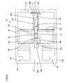
- each on-board connector 18 includes a housing 60 made of an insulating material such as a synthetic resin, and further includes a metallic output terminal 70 completely contained in the housing 60.
- the housing 60 is a single-piece component that includes a terminal holding portion 61 and an insulating portion 62.
- the terminal holding portion 61 forms a block-like shape, in which an engaging recess 63 is formed so as to have a vertically-elongated rectangular opening on the outer surface (i.e., the circuit board 17 facing surface) of the housing 60.
- the position and size of the engaging recess 63, when the on-board connector 18 is mounted to the circuit board 17, are set to correspond substantially to those of the fitting hole 17H.
- the relay connector 14 can be fitted into the engaging recess 63.
- a pair of upper and lower positioning portions 64 are formed as rib-like protrusions so as to protrude from the inside surface closer to the edge portion 17E of the circuit board 17.
- the pair of positioning portions 64 are vertically located at substantially the center of the engaging recess 63.
- a holding groove 65 in which the output terminal 70 is mounted (or held), is provided within the terminal holding portion 61.
- the holding groove 65 is formed so as to traverse the engaging recess 63 and have an elongated opening extending on the circuit board 17 facing surface of the housing 60 and along the horizontal direction perpendicular to the edge portion 17E of the circuit board 17.
- the holding groove 65 includes a first groove portion 65a formed of a deep recess on the inside surface of the engaging recess 63 farther from the edge portion 17E of the circuit board 17, a pair of second groove portions 65b formed of recesses extending to the respective upper and lower sides from the far end portion (i.e., the end portion farthest from the edge portion 17E) of the first groove portion 65a, and a third groove portion 65c formed of a recess extending between the pair of positioning portions 64 from the inside surface of the engaging recess 63 closer to the edge portion 17E of the circuit board 17.
- the terminal holding portion 61 is formed to be larger than the insulating portion 62, described below, in thickness measured from the back surface of the circuit board 17, so that a substantially step-like shape is formed therebetween.
- a tapered surface 61S is formed on the outer surface of the terminal holding portion 61 on the opposite side of the circuit board 17, by cutting the edge of its insulating portion 62 side corner at an angle of 45°.
- the insulating portion 62 is arranged closer to the edge portion 17E of the circuit board 17 than the terminal holding portion 61, so as to be continuous with the edge portion 17E side surface of the terminal holding portion 61.
- the circuit board 17 facing surface of the insulating portion 62 is continuous and flush with the circuit board 17 facing surface of the terminal holding portion 61.
- the insulating portion 62 is the same as the terminal holding portion 61 in width (i.e., length along the vertical direction parallel to the edge portion 17E of the circuit board 17).
- the upper and lower outer surfaces of the insulating portion 62 are continuous and flush with the respective upper and lower outer surfaces of the terminal holding portion 61.
- the horizontal length (i.e., length along a direction perpendicular to the edge portion 17E of the circuit board 17) of the insulating portion 62 is substantially half the horizontal length of the terminal holding portion 61.
- the insulating portion 62 includes a pair of upper and lower thin-walled portions 62a having a block-like shape, and further includes a thick-walled portion 62b arranged between the thin-walled portions 62a and having a block-like shape.
- the insulating portion 62 when viewed from the edge portion 17E side of the circuit board 17, forms a laterally facing T-shape.
- Metallic reinforcing pins 66 elongated perpendicularly to the back surface of the circuit board 17, are embedded in the respective thin-walled portions 62a.
- One end portion of each reinforcing pin 66 projects from the circuit board 17 facing surface of the thin-walled portion 62a to the outside, and is fitted into the positioning hole 17a.
- the fitting structure between the reinforcing pin 66 and the positioning hole 17a serves as a reinforcing means for fixation of the housing 60 to the circuit board 17.
- a positioning recess 62c is formed on the thick-walled portion 62b so as to have a circular opening on its outer surface on the opposite side of the circuit board 17.
- the positioning recess 62c serves as a positioning means, when a cover not shown, or the like, is mounted to the power board 16 from the back side.
- the axis thereof is perpendicular to the back surface of the circuit board 17.
- the output terminal 70 which can be formed by bending a metallic plate that is formed into a predetermined shape by punching, includes a proximal portion 71, a supported portion 74, a flexible portion 72 and a connecting part 73.
- the output terminal 70 is mounted into the holding groove 65 from the circuit board 17 facing side of the terminal holding portion 61.
- the proximal portion 71 has a rectangular plate-like shape elongated in a direction perpendicular to the back surface of the circuit board 17, so that the surface thereof is arranged substantially parallel to the edge portion 17E of the circuit board 17.
- a connecting pin 71a having a small width is provided on the proximal end of the proximal portion 71.
- the proximal portion 71 is held in the second groove portion 65b by press fitting, while small protruding parts formed on the lateral edge portions of the proximal portion 71 wedge into the inner walls of the second groove portions 65b. Consequently, the output terminal 70 is held so as to be substantially completely contained in the terminal holding portion 61, except for the connecting pin 71a.
- the connecting pin 71a penetrates through a connecting hole 17b of the circuit board 17, and is connected to the circuit.
- the housing 60 is fixed to the circuit board 17 due to the connecting pin 71a fitted into the connecting hole 17b.
- the supported portion 74 generally forms an elongated shape having a width smaller than that of the proximal portion 71, and is arranged in the deep portion of the first groove portion 65a, i.e., arranged away from the opening thereof.
- the supported portion 74 extends substantially orthogonally from the end portion of the proximal portion 71 on the opposite side of the connecting pin 71a toward the edge portion 17E side of the circuit board 17. That is, the supported portion 74 is elongated in a direction substantially parallel to the back surface of the circuit board 17 and substantially perpendicular to the edge portion 17E of the circuit board 17.
- the supported portion 74 is smaller than the proximal portion 71 in length.
- the flexible portion 72 generally forms an elongated shape having the same width as the supported portion 74, and extends substantially orthogonally (or substantially parallel to the proximal portion 71) from the distal end (i.e., the end portion on the opposite side of the proximal portion 71) of the supported portion 74.
- the flexible portion 72 is slightly smaller than the proximal portion 71 in length.
- the flexible portion 72 is held in the first groove portion 65a, so as to be capable of being slanted at an acute or obtuse angle to the supported portion 74, due to its elastic deformation.
- the connecting part 73 generally forms an elongated shape having the same width as the flexible portion 72, and specifically forms a substantially U-shape having a narrowed open end.
- the connecting part 73 includes a first strip portion 73a that loops back at the distal end of the flexible portion 72 and extends in a direction away from the circuit board 17, and further includes a second strip portion 73b that loops back at the distal end of the first strip portion 73a and extends in a direction toward the circuit board 17.
- the distance between the strip portions 73a, 73b is partly set to be shorter. The shorter-distance portions of the strip portions 73a, 73b are located in the engaging recess 63.
- the first strip portion 73a is arranged along the inside surface of the engaging recess 63 farther from the edge portion 17E of the circuit board 17, so as to be partly contained in the first groove portion 65a.
- the second strip portion 73b is arranged along the inside surface of the engaging recess 63 closer to the edge portion 17E of the circuit board 17, so as to be partly contained in the third groove portion 65c (or partly arranged between the pair of positioning portions 64) .
- the power board 16, thus constructed, is mounted to the chassis 13 by being moved toward the chassis 13 from the back side while the circuit board 17 is kept parallel to the chassis 13.
- the mounting direction of the on-board connectors 18 to the relay connectors 14 is directly opposite to the mounting direction of the discharge tube 15 to the relay connectors 14. That is, the fitting direction of the on-board connectors 18 is parallel to the mounting direction of the discharge tube 15 to the relay connectors 14.
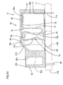
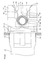
- the wall portion 27 of each relay connector 14 and the board connecting portion 33 arranged along the wall portion 27 penetrate the circuit board 17 through the fitting hole 17H, and are inserted into the engaging recess 63 of the on-board connector 18 so as to be placed between the first strip portion 73a and the second strip portion 73b, as shown in FIGS.
- the wall portion 27 has contact with the first strip portion 73a, while the board connecting portion 33 has contact with the second strip portion 73b. Further, the connecting part 73 deforms elastically so as to increase the distance between the first strip portion 73a and the second strip portion 73b.
- the relay connector 14 is thus fitted into the on-board connector 18, and thereby the relay terminal 30 is conductively connected to the output terminal 70. Consequently, the power board 16 is connected to the discharge tubes 15 via the relay connectors 14, so that the power from the power board 16 can be supplied to the discharge tubes 15.
- the on-board connectors 18 have reached a proper state of being fitted onto the relay connectors 14, the power board 16 is screwed to the chassis 13.
- the relay terminal 30 is movably fitted into the engaging recess 63. That is, it is fitted as shown in FIG. 9 so that the clearance space 27c is left between the relay terminal 30 and the engaging recess 63.
- the dimensions of the relay terminal 30 and the output terminal 70 are designed so that the connection therebetween can be maintained even when the relay terminal 30 moves or displaces within the engaging recess 63.
- the margin (or allowance) for connection between the board connecting portion 33 and the connecting part 73 is designed to be larger than the width of the clearance space 27c.
- the fitting holes 17H are formed as through holes on the circuit board 17. This enables the on-board connectors 18, provided for connection to the relay terminals 30 on the chassis 13, to be arranged on the back surface of the circuit board 17 on the opposite side of the chassis 13. On the other hand, the electronic components 19 free from restriction of the positional relationship with the chassis 13 can be mounted on the back surface of the circuit board 17, as are the on-board connectors 18.
- the power board 16 connected to the relay terminals 30 on the chassis 13 can be achieved as a single-sided power board in which the back surface on the opposite side of the chassis 13 is provided as the single mounting surface.
- the output terminal 70 is locked by the positioning portions 64 provided on the inside surface of the engaging recess 63, so that displacement of the output terminal 70 in the vertical direction parallel to the edge portion 17E of the circuit board 17 is restricted. Therefore, the flexural rigidity of the output terminal 70 is not required to be increased for displacement prevention.
- the reduced flexural rigidity of the output terminal 70, thus provided, results in reduction of the frictional resistance developed when the relay terminal 30 is connected to the output terminal 70. Thus, the operational efficiency when the relay terminal 30 is connected to the output terminal 70 can be improved.
- the output terminal 70 is formed to include a proximal portion 71 fixed to the housing 60, a flexible portion 72 extending from the proximal portion 71 (via the supported portion 74) and capable of elastic deflection, and a substantially U-shaped connecting part 73 extending from the flexible portion 72 and capable of elastically pinching the relay terminal 30.
- the board connecting portion 33 of the relay terminal 30 can have contact solely with the second strip portion 73b of the two strip portions 73a, 73b of the connecting part 73, i.e., the free-end-side strip portion on the opposite side of the flexible portion 72.
- the whole connecting part 73 i.e., both of the first strip portion 73a and the second strip portion 73b
- the flexible portion 72 side or to the proximal portion 71 side
- the connection between the board connecting portion 33 and the second strip portion 73b can be maintained.
- the board connecting portion 33 relatively moves to the free end side or to the opposite side of the flexible portion 72
- the second strip portion 73b on the free end side is pushed by the relay terminal 30 into movement, without noticeable elastic deflection of the flexible portion 72. Then, the connection between the board connecting portion 33 and the second strip portion 73b can be also maintained. Note that the first strip portion 73a at the time is disengaged from the wall portion 27.
- the output terminals 70 may displace in the array direction from the relay terminals 30 due to some reason such as the difference in thermal expansion rate between the nonmetallic circuit board 17 as a mounting base for the on-board connectors 18 and the metallic chassis 13 as a mounting base for the relay terminals 30.
- the connecting part 73 is provided on the output terminal 70 so as to be elongated in a direction substantially perpendicular to the array direction of the on-board connectors 18 (i.e., in the horizontal direction in FIG.
- the board connecting portion 33 is provided on the relay terminal 30 so as to form a plate-like shape parallel to the array direction of the on-board connectors 18 (i.e., the vertical direction in FIG. 9 ) and be larger than the connecting part 73 in width (i.e., length along a direction parallel to the array direction of the on-board connectors 18).
- the board connecting portion 33 is arranged to have contact with the connecting part 73. According to the construction, the board connecting portion 33 is set to be large in length along the array direction of the on-board connectors 18, and therefore the connection between the board connecting portion 33 and the connecting part 73 can be maintained even if the relay terminal 30 displaces in the array direction from the output terminal 70.
- the output terminal 70 is surrounded by the synthetic-resin housing 60, in which the output terminal 70 is held in the terminal holding portion 61 arranged across the insulating portion 62 from the edge portion 17E of the circuit board 17.
- the output terminals 70 are positioned in areas of the housings 60 on the opposite side of the edge portion 17E, resulting in narrow sectional arrangement.
- FIGS. 17 to 28 an embodiment 2 of the present invention will be explained with reference to FIGS. 17 to 28 .
- the construction of the lighting device 110 of a display device D differs from that of the above embodiment 1.
- the other constructions are similar to the above embodiment 1. Therefore, the same constructions are designated by the same symbols, and explanations for the constructions, operations and effects thereof are omitted.
- the lighting device 110 includes a lamp unit 112 and power boards 116, as shown in FIGS. 17 and 18 .
- the lamp unit 112 includes a metallic chassis 113, which generally forms a horizontally-elongated rectangular plate and functions as a reflector plate. Further included are a plurality of discharge tubes 115 held in a horizontal position and vertically arranged on the front side of the chassis 113 so as to be parallel to one another, and a plurality of relay connectors 114 which are vertically arranged along the lateral edges of the chassis 113 so as to correspond to the discharge tubes 115.
- the power boards 116 are disposed on the back side of the chassis 113 so as to supply power to the discharge tubes 115 via the relay connectors 114.
- a plurality of substantially rectangular mounting holes 113H corresponding to the ends of the discharge tubes 115 are formed through the chassis 113 so as to extend from the front side to the back side, and are vertically arranged to be level with the respective discharge tubes 115.
- the relay connectors 114 are mounted through the respective mounting holes 113H (See FIGS. 22 and 23 ).
- each relay connector 114 includes a holder 120 made of synthetic resin, and a relay terminal 131 that is housed in the holder 120 and made of metal (e.g., stainless steel).
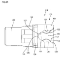
- the holder 120 includes a box-like portion 121 that forms a block-like shape as a whole, and further includes a wall portion 122 that projects backward from the back surface of the box-like portion 121.
- a container room 123 is formed in the box-like portion 121, so as to have an opening extending from the front side to the lateral side (i.e., the lateral side on the opposite side of the lateral edge portion of the chassis 113).
- the front opening portion of the opening of the container room 123 is provided as a receiving opening 124, into which an end portion (or ferrule 136) of the discharge tube 115 is fitted from the front side.
- the lateral opening portion is provided as an escape opening 125 for preventing interference with the glass tube 134 when the end portion of the discharge tube 115 is held in the container room 123.
- a stopper 126 is formed on the escape opening 125, so as to bulge inward from the opening edge and form a plate-like shape. Due to the stopper 126, the escape opening 125 is narrowed so as to form a substantially U-shaped opening.
- the vertical size of the substantially U-shaped escape opening 125 is set to be smaller than the inner diameter of the body 137 of the ferrule 136 and be equal to or slightly larger than the outer diameter of the glass tube 134 of the discharge tube 115.
- a concave portion 127 having a semicircular shape is formed on the far end portion of the opening edge.
- the radius of curvature of the concave portion 127 is set to be equal to or slightly larger than the radius of curvature of the outer circumference of the glass tube 134.
- a pair of upper and lower guiding portions 128 are formed on areas of the opening edge on the front side of the concave portion 127.
- an extended portion 129 extending parallel to the chassis 113 is formed on the lateral surface of the box-like portion 121 that includes the escape opening 125.
- the extended portion 129 extends so as to separate the front surface of the chassis 113 from the escape opening 125.
- a pair of upper and lower retaining protrusions 130 are formed on the outer surface (i.e., upper surface and lower surface) of the box-like portion 121.
- the relay terminal 131 is held within the holder 120.
- the relay terminal 131 can be formed by bending a metallic plate that is formed into a predetermined shape by punching.
- the relay terminal 131 includes a pair of vertically symmetrical elastic pressing parts 132 formed of curved plates, and further includes a board connecting portion 133 formed as a flat plate-like portion that projects to the back side.
- the pair of elastic pressing parts 132 which are housed in the container room 123, can deflect elastically and vertically so as to increase distance therebetween.
- the vertical distance between the pair of elastic pressing parts 132 is shortest at a position corresponding to the front side of the concave portion 127 of the stopper 126.
- the minimum distance between the elastic pressing parts 132, when the elastic pressing parts 132 are not forced into elastic deflection or are in a free state, is set to be smaller than the outer diameter of the body 137 of the ferrule 136 attached on the discharge tube 115.
- the board connecting portion 133 projects from the back surface of the box-like portion 121 so as to be exposed to the outside of the holder 120, and extends backwards along the wall portion 122.
- the wall portion 122 of the holder 120 is inserted into a mounting hole 113H from the front side of the chassis 113 as shown in FIGS. 22 and 23 .
- the outer surface of the box-like portion 121 becomes in contact with the opening edge of the mounting hole 113H on the front surface of the chassis 113, while the retaining protrusions 130 are locked by the opening edge of the mounting hole 113H on the back surface of the chassis 113.
- the chassis 113 is sandwiched between the engaging surfaces 130 on the front side and the retaining protrusions 130 on the back side.
- the holder 120 is fixed to the chassis 113 so that its movement in the mounting direction (i.e., the through direction of the mounting hole 113H) is restricted. Then, the mounting of the relay connector 114 to the chassis 113 is completed.
- the box-like portion 121 as the front end portion of the holder 120 projects (or is exposed) to the front side of the chassis 113 while the wall portion 122 as the back end portion of the holder 120 projects (or is exposed) to the back side of the chassis 113.
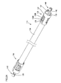
- each discharge tube 115 is formed of a cold cathode fluorescent tube that includes a generally elongated straight glass tube 134 having a circular cross section, and elongated metallic (e.g., nickel or cobalt metal) outer leads 135 which have a circular cross section and project linearly from the respective ends of the glass tube 134 and coaxially with the glass tube 134. Further included are ferrules 136 attached to the respective end portions of the glass tube 134. Mercury is encapsulated in the glass tube 134. Each end portion of the glass tube 134 is melted into a substantially hemispherical shape by heat, and thereby forms a domed portion. The outer lead 135 penetrates the domed portion.
- metallic e.g., nickel or cobalt metal
- each ferrule 136 is a single-piece component, which can be formed by bending or hammering a metallic (e.g., stainless steel) plate that is formed into a predetermined shape by punching.
- the ferrule 136 includes a body 137 and a conductive part 140.
- the body 137 generally forms a cylindrical shape concentric with the glass tube 134.
- the inner diameter of the body 137 is set to be slightly larger than the outer diameter of the glass tube 134.
- a first elastic gripping part 138A i.e., one of a pair of elastic gripping parts 138A, 138B, is generally formed as a cantilevered portion extending posteriorly (specifically, in an oblique direction slightly leaning radially inwardly), which is capable of elastic and radial deflection with a supported point on its proximal end (or anterior end).
- a curved portion 139 is formed on the distal end portion (or posterior end portion) of the first elastic gripping part 138A, so as to curve in an oblique direction leaning radially outwardly.
- the outer surface of the curve (or inwardly facing surface) of the curved portion 139 is provided as a contact point when abutting on the outer circumferential surface of the glass tube 134.
- the imaginary line that connects the contact points provided on the three first elastic gripping parts 138A forms a circle concentric with the body 137.
- the diameter of the imaginary circle, when the first elastic gripping parts 138A are not forced into elastic deflection or are in a free state, is set to be smaller than the outer diameter of the glass tube 134.
- a second elastic gripping part 138B i.e., the other of the pair of elastic gripping parts 138A, 138B, is arranged circumferentially adjacent to the first elastic gripping part 138A, and is generally formed as a cantilevered portion extending anteriorly or reversely from the first elastic gripping part 138A (specifically, in an oblique direction slightly leaning radially inwardly), which is capable of elastic and radial deflection with a supported point on its proximal end (or posterior end).
- the distal end of the second elastic gripping part 138B is provided as a contact point when abutting on the outer circumferential surface of the glass tube 134.
- the imaginary line that connects the contact points provided on the three second elastic gripping parts 138B forms a circle concentric with the body 137.
- the diameter of the imaginary circle, when the second elastic gripping parts 138B are not forced into elastic deflection or are in a free state, is set to be smaller than the outer diameter of the glass tube 134.
- a pair of protector parts are formed as cantilevered portions protruding anteriorly from the anterior end edge thereof.
- the pair of protector parts are arranged circumferentially spaced apart, and extend linearly from the body 137 so as to be flush therewith.
- the conductive part 140 is provided as a cantilevered portion that extends anteriorly from between the pair of protector parts.
- the conductive part 140 includes a long portion 141 continuous with the anterior end of the body 137, and a cylindrical portion 142 that further projects anteriorly from the anterior end (or distal end) of the long portion 141.
- the long portion 141 includes a proximal portion 141a that extends from the body 137 so as to be flush with the body 137 and parallel to the axis thereof, and further includes an intermediate portion 141b that extends radially inwardly from the distal end of the proximal portion 141a toward the axis of the body 137. Further included is a distal portion 141c that extends from the distal end of the intermediate portion 141b and parallel to the axis of the body 137.
- the cylindrical portion 142 is connected to the distal end of the distal portion 141c.
- the width of the long portion 141 is set to be sufficiently small for the length of the long portion 141.
- the long portion 141 is capable of elastic deformation in the radial direction of the body 137, elastic deformation in a direction intersecting with the radial direction (and intersecting with the longitudinal direction of the long portion 141), and elastic torsional deformation around the long portion 141 itself as the axis.
- the cylindrical portion 142 which can be formed by bending a portion laterally extending from the distal end of the long portion 141 into a cylindrical shape, is arranged substantially coaxially with the body 137.
- the cylindrical portion 142 is capable of displacement around the axis of the ferrule 136 and radial displacement, due to elastic deflection of the long portion 141.
- the tip of the outer lead 135 having passed through the body 137 begins to enter the hollow of the cylindrical portion 142.
- the ferrule 136 and the glass tube 134 are axially positioned in proper positions, resulting in the tip end portion of the outer lead 135 circumferentially surrounded by the cylindrical portion 142.
- the tip end portion of the outer lead 135 will not greatly protrude from the anterior end of the cylindrical portion 142. That is, it slightly protrudes out of the cylindrical portion 142, or is aligned with the anterior end of the cylindrical portion 142, or alternatively it is located within the cylindrical portion 142. Thereafter, the cylindrical portion 142 is clamped so as to deform with diameter reduction.
- the cylindrical portion 142 is electrically conductively fixed to the outer lead 135 by welding, and consequently the ferrule 136 is integrated with the glass tube 134. Then, the assembling process terminates, and the discharge tube 115 is completed.
- the ferrule 136 is attached to the glass tube 134, the body 137 is concentrically held on the glass tube 134 due to the elastic holding function of the three pairs of elastic gripping parts 138A, 138B.
- a gap (airspace) is secured between the outer circumference of the glass tube 134 and the inner circumference of the body 137, so as to extend over the substantially entire circumference.
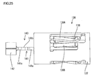
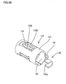
- a U-shaped connecting portion 142a may be provided as shown in FIGS. 36 and 37 .
- the U-shaped connecting portion 142a is bended so as to hug the outer lead 135, in order to achieve electrical connection between the outer lead 135 and the connecting portion 142a.
- electrical connectivity with the outer lead 135 can be further improved.
- the discharge tube 115 is fixed to relay connectors 114.
- the discharge tube 115 held in a horizontal position is moved toward the front face of the chassis 113, and the end portions and the ferrules 136 of the glass tube 134 are fitted into the container rooms 123 of the relay connectors 114 from the front side.
- the pair of elastic pressing parts 132 are pushed by the body 137 of the ferrule 136 so as to open vertically due to elastic deflection.
- the body 137 After the body 137 has passed through the shortest-distance portions of the pair of elastic pressing parts 132, the body 137 is pulled deep into the container room 123 due to elastic restoring forces of the elastic pressing parts 132, resulting in the body 137 abutting on the bottom of the container room 123. Then, the mounting of the discharge tube 115 is completed.
- the discharge tube 115 thus mounted is held by the pairs of elastic pressing parts 132 at its end portions, and consequently is fixed to the chassis 113 via the relay terminals 131 and the holders 120 provided as the relay terminal 131 mounting bases.
- the weight of the discharge tube 115 is received solely by the chassis 113 via the relay connectors 114. That is, the outer leads 135 will not be under load due to the weight of the discharge tube 115.
- the pair of elastic pressing parts 132 can have elastic contact with the outer circumferential surface of the body 137, and thereby the outer lead 135 is electrically conductively connected to the relay terminal 131 via the ferrule 136. Further, the glass tube 134 is held due to elastic restoring forces of the pair of elastic pressing parts 132, so as to be pressed against the concave portion 127 of the stopper 126. Therefore, when viewed along the axial direction of the discharge tube 115, the body 137 appears to be positioned so as to partially overlap with the stopper 126. That is, the end edge of the body 137 on the opposite side of the conductive part 140 is axially positioned in proximity to the stopper 126 so as to be partially faced therewith.
- the extended portion 129 is formed on the outer surface of the holder 120, which is perpendicular to the surface of the chassis 113 and includes the escape opening 125 of the container room 123, so as to protrude from between the chassis 113 and the escape opening 125 and extend along the surface of the chassis 113. This results in a long creepage distance from the inside of the container room 123 to the front surface of the chassis 113. Thereby, a leak, from the discharge tube 115 held in the container room 123 to the chassis 113 outside the holder 120, can be prevented.
- each power board 116 includes a circuit board 117 having a circuit formed on its back surface (i.e., the surface on the opposite side of the chassis 113), electronic components 119 mounted on the back surface of the circuit board 117, and a plurality of on-board connectors 118 mounted on the back surface of the circuit board 117.
- the circuit board 117 has a vertically-elongated rectangular shape as a whole, and is formed using a phenolic paper-base copper-clad laminated board (known as a phenolic paper).
- a plurality of fitting holes 117H having a vertically-elongated rectangular shape are formed through the circuit board 117 so as to extend from the front side to the back side.
- the plurality of fitting holes 117H are arranged vertically along the lateral side edge of the circuit board 117 so as to correspond to the above-described relay terminals 131 (or relay connectors 114).
- Each on-board connector 118 includes a housing made of synthetic resin, and an output terminal (not shown) that is completely contained in the housing and made of metal (e.g., nickel silver).
- the on-board connectors 118 are arranged along the lateral side edge of the circuit board 117 so as to correspond to the respective fitting holes 117H.
- a fitting space (not shown) is formed on the outer surface of the housing so as to correspond to the fitting hole 117H, and the output terminal is partly exposed to the fitting space.
- the power board 116 is moved toward the chassis 113 from the back side and is fixed thereto.
- the wall portions 122 of the relay connectors 114 and the board connecting portions 133 arranged along the wall portions 122 penetrate the circuit board 117 through the fitting holes 117H and are inserted into the engaging recesses 127 of the on-board connectors 118.
- the on-board connectors 118 are fitted onto the relay connectors 114, and the output terminals are conductively connected to the relay terminals 131.
- the stoppers 126 lock the ferrules 136. Therefore, the discharge tube 115 is secure from axial movement relative to the relay connectors 114. That is, if a force is applied to the discharge tube 115 so as to cause movement to the right, the stopper 126 catches the left-adjacent ferrule 136 attached on the left end portion of the discharge tube 115 so that the movement of the discharge tube 115 to the right is restricted.
- the stopper 126 catches the right-adjacent ferrule 136 attached on the right end portion of the discharge tube 115 so that the movement of the discharge tube 115 to the left is restricted.
- the axial movement of the discharge tube 115 to either right or left is restricted, and therefore the tip of the outer lead 135 is secure from hitting the wall 122 of the container room 123 on the opposite side of the escape opening 125.
- the stopper 126 can engage with and lock the end edge of the ferrule 136, and therefore a hole that can engage with the stopper 126 is not required to be formed on the outer circumference of the ferrule 136. Thereby, processing cost can be reduced, and reduction in strength of the ferrule 136 can be prevented.
- the conductive part 140 extending from the end edge of the ferrule 136 may preclude the end edge of the ferrule 136 from engaging with the stopper 126, when the ferrule 136 is attached at some angle about its axis.
- the stopper 126 is arranged to engage with the end edge on the opposite side of the conductive part 140. Therefore, the conductive part 140 will not preclude the ferrule 136 from engaging with the stopper 126, and consequently the ferrule 136 can infallibly engage with the stopper 126.
- the conductive part 140 includes a cylindrical portion 142, which can be circumferentially connected to the outer lead 135 so as to surround it. Thereby, the conductive part 140 can be prevented from disengaging from the outer lead 135. That is, the cylindrical portion 142 will not disengage from the outer lead 135 when the cylindrical portion 142 is clamped. Therefore, the conductive part 140 can be infallibly connected to the outer lead 135.
- the margin for engagement of a ferrule 136 with a stopper 126 corresponds to half of the dimensional difference between the outer diameters of the glass tube 134 and the ferrule 136.
- ferrules 136 are concentrically held on a glass tube 134 due to the elastic gripping parts 138A, 138B. Therefore, if the ferrule 136 is set to be large, a large dimensional difference can be secured between the inner diameter thereof and the outer diameter of the glass tube 134. Thereby, the margin for engagement of the ferrule 136 with the stopper 126 can be increased, resulting in reliable restriction of movement of the discharge tube 115.
- the concave portion 127 is formed on a stopper 126, so as to abut on the outer circumference of a glass tube 134 when the ferrule 136 engages with the stopper 126.
- the pair of elastic pressing parts 132 capable of pressing the discharge tube 115 toward the concave portion 127 side are provided in the relay connector 114. Specifically, the pair of elastic pressing parts 132 press the discharge tube 115 toward the concave portion 127 side, obliquely from above and obliquely from below, i.e., vertically symmetrically. Thereby, the glass tube 134 is prevented from disengaging from the concave portion 127, and therefore the engagement of the ferrule 136 with the stopper 126 can be reliably maintained.
- the relay connector 114 is formed by mounting a relay terminal 131 in a holder 120 made of synthetic resin.
- the stopper 126 is formed on the synthetic-resin holder 120. Therefore, a stopper is not required to be formed on the relay terminal 131, and thereby the material for manufacturing the relay terminals 131 can be reduced. Considering that the material cost for synthetic resin is generally lower than that for metal, the material cost for relay connectors 114 can be reduced according to the present embodiment 2.
- FIGS. 29 to 35 an embodiment 3 of the present invention will be explained with reference to FIGS. 29 to 35 .
- the constructions of means for supporting a discharge tube 115 differ from those of the above embodiment 2.
- the other constructions are similar to the above embodiment 2. Therefore, the same constructions are designated by the same symbols, and explanations for the constructions, operations and effects thereof are omitted.
- the end portions of a discharge tube 115 are supported by relay connectors 114, each of which includes a holder 120 and a relay terminal 131.
- relay connectors 114 each of which includes a holder 120 and a relay terminal 131.
- one of the end portions of a discharge tube 115 is supported by the same relay connector 114 as the embodiment 2, while the other end portion of the discharge tube 115 is supported by a grounding member 150.
- the grounding member 150 includes an elongated support plate 151 fixed to the chassis 113 so as to be along one of the lateral edge portions thereof, and further includes a plurality of grounding terminals 152 conductively mounted on the front surface of the support plate 151.
- Mounting holes 151H are formed through the support plate 151 so as to correspond three-to-one with the grounding terminals 152.
- the support plate 151 is formed of a substrate or a metallic plate.
- each grounding terminal 152 which can be formed by bending a metallic (e.g., nickel silver) plate that is formed into a predetermined shape by punching, includes a base portion 153 and a pair of elastic pressing parts 154 which extend vertically symmetrically from the respective upper and lower edge portions of the base portion 153 to the front side. Further included is a stopper 155 that extends from one of the lateral edge portions of the base portion 153 to the front side.
- the pair of elastic pressing parts 154 are provided on the lateral edge portion on the opposite side of the stopper 155, so as to form bulging curves toward each other.
- the elastic pressing parts 154 are capable of elastic deflection so as to increase the distance therebetween.
- the minimum distance between the pair of elastic pressing parts 154, when the elastic pressing parts 154 are free from elastic deflection, is set to be smaller than the outer diameter of the glass tube 134 of a discharge tube 115.
- the stopper 155 is raised from the base portion 153, so as to form a right angle with the axis of the discharge tube 115.
- a concave portion 156 is formed on the stopper 155, so as to sag in a substantially circular arc.
- a pair of guiding portions 128 are raised from the respective upper and lower sides of the concave portion 127 of the stopper 126.
- the heights of portions raised from the respective upper and lower sides of the concave portion 156 of the base portion 153 are reduced to be short. That is, means corresponding the guiding portions 128 of the embodiment 2 are not provided. Therefore, metallic material required for grounding terminals 152 can be reduced, compared to including guiding portions.
- Three leg portions 157 are further formed on the base portion 153, so as to be integrated therewith. Two of the three leg portions 157 are provided between the elastic pressing parts 154 and the stopper 155, so as to project from the respective upper and lower edge portions of the base portion 153 to the opposite side of the elastic pressing parts 154 or the stopper 155 (i.e., to the back side). The remaining one of the leg portions 157 is provided on the lateral edge of the base portion 153 on the opposite side of the stopper 155, so as to project from the intermediate position between the elastic pressing parts 154 to the opposite side of the elastic pressing parts 154 or the stopper 155 (i.e., to the back side).
- the grounding terminal 152 is not housed in a member such as a plastic housing, i.e., barely provided as shown in FIG. 343, and is conductively fixed to the support plate 151 by soldering or the like so that its leg portions 157 penetrate through the mounting holes 151H.
- the plurality of grounding terminals 152 are mounted to the common support plate 151, and thereby are conductively connected to one another via the support plate 151.
- Power boards are not connected to the grounding members 150, and the support plate 151 is conductively connected to the chassis.
- the body 137 After the body 137 has passed through the shortest-distance portions of the pair of elastic pressing parts 154, the body 137 is pulled toward the base portion 153 side due to elastic restoring forces of the elastic pressing parts 154, resulting in the body 137 abutting on the base portion 153. Then, the fixation of the discharge tube 115 is completed. The other end portion of the discharge tube 115 is fixed to a relay connector 114 in a similar manner to the above embodiment 2.
- the body 137 when viewed along the axial direction of the discharge tube 115, the body 137 appears to be positioned so as to partially overlap with the stopper 126 or 155. That is, the end edge of the body 137 on the opposite side of the conductive part 40 is axially positioned in proximity to the stopper 126 or 155 so as to be partially faced therewith.
- protector portions 551 may be provided on the grounding terminal 152.
- Each protector portion 551 includes a restricting portion 552 for an elastic pressing part, and further includes an abutting portion 553 for abutting on the support plate.
- the abutting portions 553 abut on or are located close to the support plate 151. If some kind of external force is applied to the elastic pressing parts 154 so that they are pushed to open, they first become in contact with the restricting portions 553 during the course of opening.
- the abutting portions 553 serve as supports for preventing the protector portions 551 from collapsing, when an additional load is thereafter applied.
- the stopper 126 of the holder 120 and the stopper 155 of the grounding terminal 152 lock the ferrules 136 on the respective ends of the discharge tube 115. Therefore, the discharge tube 115 is secure from axial movement relative to the relay connector 114. That is, if a force is applied to the discharge tube 115 so as to cause movement from the relay connector 114 side to the grounding member 150 side, the ferrule 136 attached on the end portion of the discharge tube 115 on the relay connector 114 side is caught by the stopper 126 of the holder 120 so that the movement of the discharge tube 115 to the grounding member 150 side is restricted.
- the ferrule 136 attached on the end portion of the discharge tube 115 on the grounding member 150 side is caught by the stopper 155 of the grounding terminal 152 so that the movement of the discharge tube 115 to the relay connector 114 side is restricted.
- the axial movement of the discharge tube 115 to either right or left is restricted, and therefore the tip of the outer lead 135 is secure from hitting the wall of the container room 123 on the opposite side of the escape opening 125 or hitting the sidewall of the chassis 113.
- the concave portion 156 is formed on the stopper 155 of a grounding terminal 150, so as to abut on the outer circumference of a glass tube 134 when the ferrule 136 is engaged with the stopper 155.
- the pair of elastic pressing parts 154 capable of pressing the discharge tube 115 toward the concave portion 156 side are provided on the grounding terminal 152. Specifically, the pair of elastic pressing parts 154 press the discharge tube 115 toward the concave portion 156 side, obliquely from above and obliquely from below, i.e., vertically symmetrically.
- the glass tube 134 is prevented from disengaging from the concave portion 156, and therefore the engagement of the ferrule 136 with the stopper 155 can be reliably maintained.
- the stoppers 155 are integrated with the respective grounding terminals 152 provided as means for conductive connection to the ferrules 136. Thereby, the number of components can be reduced in the present embodiment 3, compared to including stoppers provided as separate members from the grounding terminals.
Landscapes
- Physics & Mathematics (AREA)
- Nonlinear Science (AREA)
- Mathematical Physics (AREA)
- Chemical & Material Sciences (AREA)
- Crystallography & Structural Chemistry (AREA)
- General Physics & Mathematics (AREA)
- Optics & Photonics (AREA)
- Coupling Device And Connection With Printed Circuit (AREA)
- Liquid Crystal (AREA)
- Arrangement Of Elements, Cooling, Sealing, Or The Like Of Lighting Devices (AREA)
Abstract
Description
- The present invention relates to a power board, an on-board connector, a lighting device, a display device and a television receiver.
- An example of a lighting device capable of functioning as a backlight for a liquid crystal display device is disclosed in Patent Document 1. The lighting device has a construction, in which relay terminals are mounted into through holes formed on a chassis that has a substantially flat plate-like shape and functions as a reflector plate. An electrode part of a discharge tube arranged on the front side of the chassis and a power board arranged on the back side of the chassis are connected to each relay connector, so that the discharge tube can receive the power supply from the power board via the relay terminal.
- Patent Document 1:
JP-A-2004-294592 - In the power board described in the above Patent Document 1, electronic components are mounted on the surface of a circuit board on the opposite side of the chassis, while an output terminal to be fitted to the connecting member is mounted on the chassis-facing surface. In the case that components are thus mounted to both surfaces of the circuit board, there is no choice but to use reflow soldering as a soldering method for fixing the components to the circuit board, because solder dipping that involves dipping of the circuit board in a molten solder bath cannot be applied.
However, the reflow soldering cannot be applied to a circuit board formed of a material sensitive to high temperature (e.g., a phenolic paper-base copper-clad laminated board), because a reflow oven is heated to a high temperature. That is, in the case of a circuit board formed of a material sensitive to high temperature, components cannot be mounted to both surfaces of the circuit board, and therefore the components should be mounted on one surface of the circuit board.
In this case, in order to achieve an output terminal provided on the chassis-facing side of the circuit board as in Patent Document 1 for connection to the connecting member, the components on the circuit board are limited to being mounted on the chassis-facing surface.
The present invention was made in view of the foregoing circumstances, and an object thereof is to enable the surface of a single-sided power board on the opposite side of a chassis, when the power board is connected to a relay terminal on the chassis, to serve as the single mounting surface. - As a means for achieving the above object, a power board according to the present invention, which is to be mounted to the back side of a chassis having substantially a plate-like shape, includes a circuit board capable of being arranged substantially parallel to the chassis, and an on-board connector mounted to the circuit board. The output terminal of the on-board connector can be connected to a relay terminal provided on the chassis, so that power is supplied to a discharge tube arranged on the front side of the chassis. A fitting hole is formed through the circuit board so as to extend from the front surface to the back surface thereof. The on-board connector is mounted to the back surface of the circuit board, and is positioned to correspond to the fitting hole.
- The relay terminal and the output terminal can be connected to each other, while one or both thereof penetrate the circuit board through the fitting hole. The fitting hole is thus formed as a through hole on the circuit board, and thereby the on-board connector, provided for connection to the relay terminal on the chassis, can be arranged on the back surface of the circuit board on the opposite side of the chassis. On the other hand, electronic components free from restriction of the positional relationship with the chassis can be mounted on the back surface of the circuit board, as is the on-board connector. According to the present invention, the power board connected to the relay terminal on the chassis can be thus achieved as a single-sided power board in which the back surface on the opposite side of the chassis is provided as the single mounting surface.
- In the power board described above, the on-board connector can include a housing made of an insulating material, so that the output terminal is at least partly held in the housing.
- In this case, the output terminal is at least partly held in the housing, and therefore the part held in the housing can be prevented from interference with foreign substances.
- In the power board described above, an engaging recess having an opening corresponding to the fitting hole can be formed on the housing, so that the output terminal is arranged in the engaging recess.
- In this case, the relay terminal can be inserted into the engaging recess so as to be connected to the output terminal therewithin. Thereby, the connection between the terminals can be prevented from interference with foreign substances.
- In the power board described above, a positioning portion, which can lock the output terminal so that displacement of the output terminal along the inside surface of the engaging recess is restricted, may be provided on the inside surface.
- In this case, the displacement of the output terminal is restricted by the positioning portion, and therefore the flexural rigidity of the output terminal is not required to be increased for displacement prevention. The reduced flexural rigidity of the output terminal, thus provided, results in reduction of the frictional resistance developed when the relay terminal is connected to the output terminal. Thus, the operational efficiency at the time of connection can be improved.
- In the power board described above, the output terminal can include a proximal portion fixed to the housing, a flexible portion extending from the proximal portion and being capable of elastic deflection, and a connecting part extending from the flexible portion and having substantially a U-shape capable of elastically pinching the relay terminal. The connecting part may include two strip portions, so that a free-end-side strip portion of the two strip portions on the opposite side of the flexible portion can have contact with the relay terminal.
- If the relay terminal moves or displaces from the output terminal toward the flexible portion side, the whole connecting part moves to the flexible portion side, together with the relay terminal. Thus, the connection between the relay terminal and the free-end-side strip portion can be maintained. If the relay terminal moves or displaces from the output terminal to the free end side or to the opposite side of the flexible portion, the free-end-side strip portion of the connecting part is pushed by the relay terminal into movement. Then, the connection between the relay terminal and the free-end-side strip portion can be also maintained.
- In the power board described above, in a case where a plurality of on-board connectors as the above on-board connector are arranged in a line so as to be capable of corresponding to a plurality of relay terminals as the above relay terminal, the output terminal can include a connecting part that is elongated in a direction substantially perpendicular to the array direction of the on-board connectors. The connecting part can have contact with the relay terminal that forms a plate-like shape having a width larger than that of the connecting part and to be arranged parallel to the array direction of the on-board connectors.
- In the case of including a plurality of on-board connectors arranged in a line so as to correspond to a plurality of relay terminals, the output terminals of the on-board connectors may displace in the array direction from the relay terminals due to some reason such as the difference in thermal expansion rate between the circuit board as a mounting base for the on-board connectors and the chassis as a mounting base for the relay terminals. In view of this, according to the present invention, the connecting part is provided on the output terminal so as to be elongated in a direction substantially perpendicular to the array direction of the on-board connectors, while the relay terminal having a plate-like shape, wider than the connecting part and to be arranged parallel to the array direction of the on-board connectors, is provided so as to be capable of contact with the connecting part. The relay terminal is set to be large in width along the array direction, and therefore the connection between the relay terminal and the connecting part can be maintained even if the relay terminal displaces in the array direction from the output terminal.
- In the power board described above, the on-board connector can be arranged along an edge portion of the circuit board. The output terminal may be arranged on an area of the housing on the opposite side of the edge portion, so that a sectional arrangement is provided.
- In this case, the output terminal is arranged on the area of the housing on the opposite side of the edge portion of the circuit board, resulting in sectional arrangement. Consequently, a low-voltage area is left on a portion of the on-board connector located in proximity to the edge portion of the circuit board.
- As a means for achieving the above object, an on-board connector according to the present invention is provided, which is to be mounted to a circuit board in order to form a power board. The power board can be mounted to the back side of a chassis having substantially a plate-like shape, so that the circuit board is arranged substantially parallel to the chassis. The on-board connector includes an output terminal that can be connected to a relay terminal provided on the chassis so that power is supplied to a discharge tube arranged on the front side of the chassis. The on-board connector can be mounted to the back surface of the circuit board, and be positioned to correspond to a fitting hole that is formed through the circuit board so as to extend from the front surface to the back surface thereof.
- The relay terminal and the output terminal can be connected to each other, while one or both thereof penetrate the circuit board through the fitting hole. The fitting hole is thus formed as a through hole on the circuit board, and thereby the on-board connector, provided for connection to the relay terminal on the chassis, can be arranged on the back surface of the circuit board on the opposite side of the chassis. On the other hand, electronic components free from restriction of the positional relationship with the chassis can be mounted on the back surface of the circuit board, as is the on-board connector. According to the present invention, the power board connected to the relay terminal on the chassis can be thus achieved as a single-sided power board in which the back surface on the opposite side of the chassis is provided as the single mounting surface.
- The on-board connector, described above, can further include a housing made of an insulating material, so that the output terminal is at least partly held in the housing.
- In this case, the output terminal is at least partly held in the housing, and therefore the part held in the housing can be prevented from interference with foreign substances.
- In the on-board connector described above, an engaging recess, having an opening capable of being arranged to correspond to the fitting hole, can be formed on the housing, so that the output terminal is arranged in the engaging recess.
- In this case, the relay terminal can be inserted into the engaging recess so as to be connected to the output terminal therewithin. Thereby, the connection between the terminals can be prevented from interference with foreign substances.
- In the on-board connector described above, a positioning portion, which can lock the output terminal so that displacement of the output terminal along the inside surface of the engaging recess is restricted, may be provided on the inside surface.
- In this case, the displacement of the output terminal is restricted by the positioning portion, and therefore the flexural rigidity of the output terminal is not required to be increased for displacement prevention. The reduced flexural rigidity of the output terminal, thus provided, results in reduction of the frictional resistance developed when the relay terminal is connected to the output terminal. Thus, the operational efficiency at the time of connection can be improved.
- In the on-board connector described above, the output terminal can include a proximal portion fixed to the housing, a flexible portion extending from the proximal portion and being capable of elastic deflection, and a connecting part extending from the flexible portion and having substantially a U-shape capable of elastically pinching the relay terminal. The connecting part may include two strip portions, so that a free-end-side strip portion of the two strip portions on the opposite side of the flexible portion can have contact with the relay terminal.
- If the relay terminal moves or displaces from the output terminal toward the flexible portion side, the whole connecting part moves to the flexible portion side, together with the relay terminal. Thus, the connection between the relay terminal and the free-end-side strip portion can be maintained. If the relay terminal moves or displaces from the output terminal to the free end side or to the opposite side of the flexible portion, the free-end-side strip portion of the connecting part is pushed by the relay terminal into movement. Then, the connection between the relay terminal and the free-end-side strip portion can be also maintained.
- In the on-board connector described above, in a case where a plurality of housings as the above housing are arranged in a line so as to be capable of corresponding to a plurality of relay terminals as the above relay terminal, the output terminal can include a connecting part that is elongated in a direction substantially perpendicular to the array direction. The connecting part can have contact with the relay terminal that forms a plate-like shape having a width larger than that of the connecting part and to be arranged parallel to the array direction.
- In the case of including a plurality of on-board connectors arranged in a line so as to correspond to a plurality of relay terminals, the output terminals of the on-board connectors may displace in the array direction from the relay terminals due to some reason such as the difference in thermal expansion rate between the circuit board as a mounting base for the on-board connectors and the chassis as a mounting base for the relay terminals. In view of this, according to the present invention, the connecting part is provided on the output terminal so as to be elongated in a direction substantially perpendicular to the array direction of the on-board connectors, while the relay terminal having a plate-like shape, wider than the connecting part and to be arranged parallel to the array direction of the on-board connectors, is provided so as to be capable of contact with the connecting part. The relay terminal is set to be large in width along the array direction, and therefore the connection between the relay terminal and the connecting part can be maintained even if the relay terminal displaces in the array direction from the output terminal.
- In the on-board connector described above, the housing can be arranged along an edge portion of the circuit board. The output terminal may be arranged on an area of the housing that can be positioned on the opposite side of the edge portion, so that a sectional arrangement is provided.
- In this case, the output terminal is arranged on the area of the housing that can be positioned on the opposite side of the edge portion of the circuit board, resulting in sectional arrangement. Consequently, a low-voltage area is left on a portion of the on-board connector located in proximity to the edge portion of the circuit board.
- A lighting device according to the present invention includes a power board according to the present invention described above, a chassis and a discharge tube.
- A display device according to the present invention includes a lighting device according to the present invention described above, and a display panel arranged on the front side of the lighting device.
A television receiver according to the present invention includes a display device according to the present invention described above. -
- [
FIG. 1 ] is a horizontal sectional view of a display device according to an embodiment 1; - [
FIG. 2 ] is a perspective view of a lighting device; - [
FIG. 3 ] is a rear view of the lighting device; - [
FIG. 4 ] is a perspective view of a power board; - [
FIG. 5 ] is a front view of the power board; - [
FIG. 6 ] is a perspective view of an on-board connector; - [
FIG. 7 ] is a perspective view of the on-board connector; - [
FIG. 8 ] is a front view of the on-board connector; - [
FIG. 9 ] is a front view of the on-board connector into which a relay connector is fitted; - [
FIG. 10 ] is a horizontal sectional view of the on-board connector; - [
FIG. 11 ] is a horizontal sectional view showing the on-board connector mounted to a lamp unit; - [
FIG. 12 ] is a partially-enlarged sectional view of the lamp unit; - [
FIG. 13 ] is a partially-enlarged front view of the lighting device; - [
FIG. 14 ] is a perspective view of a relay connector; - [
FIG. 15 ] is a perspective view of a discharge tube; - [
FIG. 16 ] is an exploded perspective view of a television receiver; - [
FIG. 17 ] is a front perspective view of a lighting device according to an embodiment 2; - [
FIG. 18 ] is a front view of the lighting device; - [
FIG. 19 ] is a perspective view of relay connectors; - [
FIG. 20 ] is a partially-enlarged front view showing a connecting structure between a relay connector and a discharge tube; - [
FIG. 21 ] is a side view of a relay connector; - [
FIG. 22 ] is a sectional view showing that a ferrule on a discharge tube is capable of engaging with a stopper; - [
FIG. 23 ] is a sectional view showing a connecting structure between a relay connector and a power board; - [
FIG. 24 ] is a perspective view of a discharge tube; - [
FIG. 25 ] is a rear view of a ferrule; - [
FIG. 26 ] is a plan view of the ferrule; - [
FIG. 27 ] is a side view of the ferrule; - [
FIG. 28 ] is a rear perspective view of the lighting device; - [
FIG. 29 ] is a front view of a lighting device according to an embodiment 3; - [
FIG. 30 ] is a front view showing the lighting device, from which discharge tubes are detached; - [
FIG. 31 ] is a rear view of the lighting device; - [
FIG. 32 ] is a perspective view of a grounding member; - [
FIG. 33 ] is a perspective view of a grounding terminal; - [
FIG. 34 ] is a sectional view showing that a ferrule on a discharge tube is capable of engaging with a stopper; - [
FIG. 35 ] is a partially-enlarged front view showing a connecting structure between a grounding terminal and a discharge tube; - [
FIG. 36 ] is a perspective view showing a modification of a ferrule; - [
FIG. 37 ] is a side view ofFIG. 36 ; - [
FIG. 38 ] is a perspective view of a grounding terminal; and - [
FIG. 39 ] is a sectional view showing a connection between a grounding terminal shown inFIG. 38 and a ferrule. -
- 10: Lighting device
- 11: Display panel
- 13: Chassis
- 15: Discharge tube
- 16: Power board
- 17: Circuit board
- 17H: Fitting hole
- 18: On-board connector
- 30: Relay terminal
- 60: Housing
- 63: Engaging recess
- 64: Positioning portion
- 70: Output terminal
- 71: Proximal portion
- 72: Flexible portion
- 73: Connecting part
- 73a: Flexible-portion-side strip portion
- 73b: Free-end-side strip portion
- An embodiment 1 according to the present invention will be hereinafter explained with reference to
FIGS. 1 to 16 . - A display device D shown in
FIG. 16 is a so-called liquid crystal display device including adisplay panel 11 and alighting device 10 as shown inFIG. 1 , which forms a horizontally-elongated rectangular shape as a whole. Thedisplay panel 11 is disposed on the front side of thelighting device 10, so that thelighting device 10 as a backlight can illuminate thedisplay panel 11 from the back side. The display device D can be applied to a television receiver. As shown inFIG. 16 , the television receiver includes the display device D, and front and back cabinets Ca and Cb capable of holding the display device D therebetween. Further included are a power source P other than apower board 16 described below, a tuner T and a stand S.FIG. 1 schematically shows the display device D, and therefore the shapes ofrelay connectors 14, on-board connectors 18 and the like differ slightly from those in the other figures.
Thedisplay panel 11 has a well-known construction, in which liquid crystal as a material with an optical property that changes with applied voltage is disposed in the gap between a transparent TFT substrate and a transparent CF substrate. TFTs (Thin Film Transistors), as switching elements connected to a source wiring line and a gate wiring line running at right angles to each other, and pixel electrodes connected to the TFTs are provided on the TFT substrate. A color filter, on which color sections of three primary colors, i.e., Red (R), Green (G) and Blue (B), are arranged in a matrix, is provided on the CF substrate. - As shown in
FIGS. 2 and3 , thelighting device 10 includes alamp unit 12 andpower boards 16. Thelamp unit 12 includes ametallic chassis 13, which generally forms a horizontally-elongated rectangular plate and functions as a reflector plate. Further included are a plurality ofdischarge tubes 15 held in a horizontal position and vertically arranged on the front side of thechassis 13 so as to be parallel to one another, and a plurality ofrelay connectors 14 which are vertically arranged along the lateral edges of thechassis 13 so as to correspond to thedischarge tubes 15. Thepower boards 16 are disposed on the back side of thechassis 13 so as to supply power to thedischarge tubes 15 via therelay connectors 14. - A plurality of mounting
holes 13H corresponding to the ends of thedischarge tubes 15 are formed through thechassis 13 so as to extend from the front side to the back side, and are vertically arranged so as to be level with therespective discharge tubes 15. Therelay connectors 14 are mounted through the respective mountingholes 13H (SeeFIGS. 12 and13 ). As shown inFIG. 14 , eachrelay connector 14 includes aholder 20 made of synthetic resin, and ametallic relay terminal 30 housed in theholder 20.
A pair of upper and lowerelastic retaining parts 25 and a pair of right and left engagingsurfaces 26 are formed on the outer surface of theholder 20. Theholder 20 is inserted into the mountinghole 13H from the front side of thechassis 13, and is fixed to thechassis 13 due to the engagingsurfaces 26 in abutting contact with the opening edge of the mountinghole 13H on the front surface of thechassis 13 and due to the retaining protrusions of theelastic retaining parts 25 being locked by the opening edge of the mountinghole 13H on the back surface of thechassis 13. When attached to thechassis 13, the front end portion of theholder 20 projects to the front side of thechassis 13, while the back end portion of theholder 20 projects to the back side of thechassis 13. - A
container room 23 is formed in the projecting portion of theholder 20 on the front side of thechassis 13, by removing the front surface and one lateral surface thereof. A plate-like wall portion 27 is formed on the projecting portion of theholder 20 on the back side of thechassis 13. Therelay terminal 30 is disposed in theholder 20. Therelay terminal 30, which can be formed by bending a metallic plate that is formed into a predetermined shape by punching, includes atube connecting portion 31 having a pair of upper and lowerelastic nipping parts 32 formed of plates having a substantially circular arc shape, and further includes a plate-likeboard connecting portion 33 projecting to the back side. Thetube connecting portion 31 is disposed in thecontainer room 23, while theboard connecting portion 33 is arranged along thewall portion 27. - Referring to
FIG. 15 , eachdischarge tube 15 is formed of a cold cathode fluorescent tube that includes a generally elongatedstraight glass tube 40 having a circular cross section, elongated outer leads 42 which have a circular cross section and project linearly from the respective ends of theglass tube 40 and coaxially with theglass tube 40, and further includesferrules 50 attached to the respective end portions of theglass tube 40. Eachferrule 50, which can be formed by bending or hammering a metallic (e.g., copper alloy) plate that is formed into a predetermined shape by punching, includes abody 51 and aconductive part 57. Thebody 51 generally forms a cylindrical shape, which is attached on the outer circumference of theglass tube 40. Theconductive part 57 extends from the end edge of thebody 51 so as to have elastic contact with the outer periphery of theouter lead 42, and is fixed by welding. Thedischarge tube 15 is mounted to thechassis 13, so that the end portions thereof are fitted into thecontainer rooms 23 of theholders 20 whiletube connecting portions 31 have elastic contact with the outer circumferences of thebodies 51 of theferrules 50. - As shown in
FIGS. 4 and5 , eachpower board 16 includes acircuit board 17 having a circuit formed on its back surface (i.e., the surface on the opposite side of the chassis 13),electronic components 19 mounted on the back surface of thecircuit board 17, and a plurality of on-board connectors 18 mounted on the back surface of thecircuit board 17.
Thecircuit board 17 has a vertically-elongated rectangular shape as a whole, and is formed using a phenolic paper-base copper-clad laminated board (known as a phenolic paper). A plurality offitting holes 17H having a vertically-elongated rectangular shape are formed through thecircuit board 17 so as to extend from the front side to the back side. The plurality offitting holes 17H are arranged vertically along thelateral edge portion 17E (or side edge portion) of thecircuit board 17 so as to correspond to the above-described relay terminals 30 (or relay connectors 14). Further, a plurality ofpositioning holes 17a are formed through thecircuit board 17 so as to extend from the front side to the back side. The positioning holes 17a are arranged between thefitting holes 17H and the side edge of thecircuit board 17 so that a pair of upper and lower positioning holes corresponds to eachfitting hole 17H. - Referring to
FIGS. 9 to 11 , the on-board connectors 18 are arranged along the lateral edge of thecircuit board 17 so as to correspond to the respectivefitting holes 17H, and are engaged with therespective relay connectors 14 through thefitting holes 17H. As shown inFIGS. 6 to 8 , each on-board connector 18 includes ahousing 60 made of an insulating material such as a synthetic resin, and further includes ametallic output terminal 70 completely contained in thehousing 60. - The
housing 60 is a single-piece component that includes aterminal holding portion 61 and an insulatingportion 62. Theterminal holding portion 61 forms a block-like shape, in which an engagingrecess 63 is formed so as to have a vertically-elongated rectangular opening on the outer surface (i.e., thecircuit board 17 facing surface) of thehousing 60. The position and size of the engagingrecess 63, when the on-board connector 18 is mounted to thecircuit board 17, are set to correspond substantially to those of thefitting hole 17H. Therelay connector 14 can be fitted into the engagingrecess 63. In the engagingrecess 63, a pair of upper andlower positioning portions 64 are formed as rib-like protrusions so as to protrude from the inside surface closer to theedge portion 17E of thecircuit board 17. The pair ofpositioning portions 64 are vertically located at substantially the center of the engagingrecess 63. - Further, a holding
groove 65, in which theoutput terminal 70 is mounted (or held), is provided within theterminal holding portion 61. The holdinggroove 65 is formed so as to traverse the engagingrecess 63 and have an elongated opening extending on thecircuit board 17 facing surface of thehousing 60 and along the horizontal direction perpendicular to theedge portion 17E of thecircuit board 17. The holdinggroove 65 includes afirst groove portion 65a formed of a deep recess on the inside surface of the engagingrecess 63 farther from theedge portion 17E of thecircuit board 17, a pair ofsecond groove portions 65b formed of recesses extending to the respective upper and lower sides from the far end portion (i.e., the end portion farthest from theedge portion 17E) of thefirst groove portion 65a, and athird groove portion 65c formed of a recess extending between the pair ofpositioning portions 64 from the inside surface of the engagingrecess 63 closer to theedge portion 17E of thecircuit board 17. - The
terminal holding portion 61 is formed to be larger than the insulatingportion 62, described below, in thickness measured from the back surface of thecircuit board 17, so that a substantially step-like shape is formed therebetween. Atapered surface 61S is formed on the outer surface of theterminal holding portion 61 on the opposite side of thecircuit board 17, by cutting the edge of its insulatingportion 62 side corner at an angle of 45°. - The insulating
portion 62 is arranged closer to theedge portion 17E of thecircuit board 17 than theterminal holding portion 61, so as to be continuous with theedge portion 17E side surface of theterminal holding portion 61. Thecircuit board 17 facing surface of the insulatingportion 62 is continuous and flush with thecircuit board 17 facing surface of theterminal holding portion 61. The insulatingportion 62 is the same as theterminal holding portion 61 in width (i.e., length along the vertical direction parallel to theedge portion 17E of the circuit board 17). The upper and lower outer surfaces of the insulatingportion 62 are continuous and flush with the respective upper and lower outer surfaces of theterminal holding portion 61. The horizontal length (i.e., length along a direction perpendicular to theedge portion 17E of the circuit board 17) of the insulatingportion 62 is substantially half the horizontal length of theterminal holding portion 61. The insulatingportion 62 includes a pair of upper and lower thin-walled portions 62a having a block-like shape, and further includes a thick-walled portion 62b arranged between the thin-walled portions 62a and having a block-like shape. The insulatingportion 62, when viewed from theedge portion 17E side of thecircuit board 17, forms a laterally facing T-shape. Metallic reinforcingpins 66, elongated perpendicularly to the back surface of thecircuit board 17, are embedded in the respective thin-walled portions 62a. One end portion of each reinforcingpin 66 projects from thecircuit board 17 facing surface of the thin-walled portion 62a to the outside, and is fitted into thepositioning hole 17a. The fitting structure between the reinforcingpin 66 and thepositioning hole 17a serves as a reinforcing means for fixation of thehousing 60 to thecircuit board 17. Apositioning recess 62c is formed on the thick-walled portion 62b so as to have a circular opening on its outer surface on the opposite side of thecircuit board 17. Thepositioning recess 62c serves as a positioning means, when a cover not shown, or the like, is mounted to thepower board 16 from the back side. The axis thereof is perpendicular to the back surface of thecircuit board 17. - Referring to
FIGS. 7 to 11 , theoutput terminal 70, which can be formed by bending a metallic plate that is formed into a predetermined shape by punching, includes aproximal portion 71, a supportedportion 74, aflexible portion 72 and a connectingpart 73. Theoutput terminal 70 is mounted into the holdinggroove 65 from thecircuit board 17 facing side of theterminal holding portion 61.
Theproximal portion 71 has a rectangular plate-like shape elongated in a direction perpendicular to the back surface of thecircuit board 17, so that the surface thereof is arranged substantially parallel to theedge portion 17E of thecircuit board 17. A connectingpin 71a having a small width is provided on the proximal end of theproximal portion 71. Theproximal portion 71 is held in thesecond groove portion 65b by press fitting, while small protruding parts formed on the lateral edge portions of theproximal portion 71 wedge into the inner walls of thesecond groove portions 65b. Consequently, theoutput terminal 70 is held so as to be substantially completely contained in theterminal holding portion 61, except for the connectingpin 71a. The connectingpin 71a penetrates through a connectinghole 17b of thecircuit board 17, and is connected to the circuit. Thehousing 60 is fixed to thecircuit board 17 due to the connectingpin 71a fitted into the connectinghole 17b. - The supported
portion 74 generally forms an elongated shape having a width smaller than that of theproximal portion 71, and is arranged in the deep portion of thefirst groove portion 65a, i.e., arranged away from the opening thereof. The supportedportion 74 extends substantially orthogonally from the end portion of theproximal portion 71 on the opposite side of the connectingpin 71a toward theedge portion 17E side of thecircuit board 17. That is, the supportedportion 74 is elongated in a direction substantially parallel to the back surface of thecircuit board 17 and substantially perpendicular to theedge portion 17E of thecircuit board 17. The supportedportion 74 is smaller than theproximal portion 71 in length. - The
flexible portion 72 generally forms an elongated shape having the same width as the supportedportion 74, and extends substantially orthogonally (or substantially parallel to the proximal portion 71) from the distal end (i.e., the end portion on the opposite side of the proximal portion 71) of the supportedportion 74. Theflexible portion 72 is slightly smaller than theproximal portion 71 in length. Theflexible portion 72 is held in thefirst groove portion 65a, so as to be capable of being slanted at an acute or obtuse angle to the supportedportion 74, due to its elastic deformation. - The connecting
part 73 generally forms an elongated shape having the same width as theflexible portion 72, and specifically forms a substantially U-shape having a narrowed open end. The connectingpart 73 includes afirst strip portion 73a that loops back at the distal end of theflexible portion 72 and extends in a direction away from thecircuit board 17, and further includes asecond strip portion 73b that loops back at the distal end of thefirst strip portion 73a and extends in a direction toward thecircuit board 17. On the connectingpart 73, the distance between thestrip portions strip portions recess 63. Thefirst strip portion 73a is arranged along the inside surface of the engagingrecess 63 farther from theedge portion 17E of thecircuit board 17, so as to be partly contained in thefirst groove portion 65a. Thesecond strip portion 73b is arranged along the inside surface of the engagingrecess 63 closer to theedge portion 17E of thecircuit board 17, so as to be partly contained in thethird groove portion 65c (or partly arranged between the pair of positioning portions 64) . - The
power board 16, thus constructed, is mounted to thechassis 13 by being moved toward thechassis 13 from the back side while thecircuit board 17 is kept parallel to thechassis 13. The mounting direction of the on-board connectors 18 to therelay connectors 14 is directly opposite to the mounting direction of thedischarge tube 15 to therelay connectors 14. That is, the fitting direction of the on-board connectors 18 is parallel to the mounting direction of thedischarge tube 15 to therelay connectors 14. At the time of fixation, thewall portion 27 of eachrelay connector 14 and theboard connecting portion 33 arranged along thewall portion 27 penetrate thecircuit board 17 through thefitting hole 17H, and are inserted into the engagingrecess 63 of the on-board connector 18 so as to be placed between thefirst strip portion 73a and thesecond strip portion 73b, as shown inFIGS. 9 and11 . Consequently, thewall portion 27 has contact with thefirst strip portion 73a, while theboard connecting portion 33 has contact with thesecond strip portion 73b. Further, the connectingpart 73 deforms elastically so as to increase the distance between thefirst strip portion 73a and thesecond strip portion 73b. Therelay connector 14 is thus fitted into the on-board connector 18, and thereby therelay terminal 30 is conductively connected to theoutput terminal 70. Consequently, thepower board 16 is connected to thedischarge tubes 15 via therelay connectors 14, so that the power from thepower board 16 can be supplied to thedischarge tubes 15. When the on-board connectors 18 have reached a proper state of being fitted onto therelay connectors 14, thepower board 16 is screwed to thechassis 13. Note that therelay terminal 30 is movably fitted into the engagingrecess 63. That is, it is fitted as shown inFIG. 9 so that theclearance space 27c is left between therelay terminal 30 and the engagingrecess 63. The dimensions of therelay terminal 30 and theoutput terminal 70 are designed so that the connection therebetween can be maintained even when therelay terminal 30 moves or displaces within the engagingrecess 63. Specifically, the margin (or allowance) for connection between theboard connecting portion 33 and the connectingpart 73 is designed to be larger than the width of theclearance space 27c. - (1) The fitting holes 17H are formed as through holes on the
circuit board 17. This enables the on-board connectors 18, provided for connection to therelay terminals 30 on thechassis 13, to be arranged on the back surface of thecircuit board 17 on the opposite side of thechassis 13. On the other hand, theelectronic components 19 free from restriction of the positional relationship with thechassis 13 can be mounted on the back surface of thecircuit board 17, as are the on-board connectors 18. Thus, according to the present embodiment, thepower board 16 connected to therelay terminals 30 on thechassis 13 can be achieved as a single-sided power board in which the back surface on the opposite side of thechassis 13 is provided as the single mounting surface. -
- (2) The
output terminal 70 is completely contained in the housing 60 (except for the connectingpin 71a), and thereby can be protected from interference with extraneous or foreign substances. - (3) The
relay terminal 30 is inserted into the engagingrecess 63 so as to be connected to theoutput terminal 70 therewithin. Thereby, foreign substances are prevented from interference with the connection between therelay terminal 30 and theoutput terminal 70. - (4) The
output terminal 70 is locked by thepositioning portions 64 provided on the inside surface of the engagingrecess 63, so that displacement of theoutput terminal 70 in the vertical direction parallel to theedge portion 17E of thecircuit board 17 is restricted. Therefore, the flexural rigidity of theoutput terminal 70 is not required to be increased for displacement prevention. The reduced flexural rigidity of theoutput terminal 70, thus provided, results in reduction of the frictional resistance developed when therelay terminal 30 is connected to theoutput terminal 70. Thus, the operational efficiency when therelay terminal 30 is connected to theoutput terminal 70 can be improved. - (5) The
output terminal 70 is formed to include aproximal portion 71 fixed to thehousing 60, aflexible portion 72 extending from the proximal portion 71 (via the supported portion 74) and capable of elastic deflection, and a substantially U-shaped connectingpart 73 extending from theflexible portion 72 and capable of elastically pinching therelay terminal 30. Theboard connecting portion 33 of therelay terminal 30 can have contact solely with thesecond strip portion 73b of the twostrip portions part 73, i.e., the free-end-side strip portion on the opposite side of theflexible portion 72.
According to the construction, if theboard connecting portion 33 of therelay terminal 30 relatively moves toward theflexible portion 72 side within the engagingrecess 63, the whole connecting part 73 (i.e., both of thefirst strip portion 73a and thesecond strip portion 73b) moves to theflexible portion 72 side (or to theproximal portion 71 side), together with theboard connecting portion 33, while pushing theflexible portion 72 into elastic deflection. Thus, the connection between theboard connecting portion 33 and thesecond strip portion 73b can be maintained.
Conversely, if theboard connecting portion 33 relatively moves to the free end side or to the opposite side of theflexible portion 72, thesecond strip portion 73b on the free end side is pushed by therelay terminal 30 into movement, without noticeable elastic deflection of theflexible portion 72. Then, the connection between theboard connecting portion 33 and thesecond strip portion 73b can be also maintained. Note that thefirst strip portion 73a at the time is disengaged from thewall portion 27. - (6) In the construction that includes a plurality of on-
board connectors 18 and a plurality ofrelay terminals 30 arranged in lines, theoutput terminals 70 may displace in the array direction from therelay terminals 30 due to some reason such as the difference in thermal expansion rate between thenonmetallic circuit board 17 as a mounting base for the on-board connectors 18 and themetallic chassis 13 as a mounting base for therelay terminals 30.
In view of this, as shown inFIG. 9 , the connectingpart 73 is provided on theoutput terminal 70 so as to be elongated in a direction substantially perpendicular to the array direction of the on-board connectors 18 (i.e., in the horizontal direction inFIG. 9 ), while theboard connecting portion 33 is provided on therelay terminal 30 so as to form a plate-like shape parallel to the array direction of the on-board connectors 18 (i.e., the vertical direction inFIG. 9 ) and be larger than the connectingpart 73 in width (i.e., length along a direction parallel to the array direction of the on-board connectors 18). Theboard connecting portion 33 is arranged to have contact with the connectingpart 73.
According to the construction, theboard connecting portion 33 is set to be large in length along the array direction of the on-board connectors 18, and therefore the connection between theboard connecting portion 33 and the connectingpart 73 can be maintained even if therelay terminal 30 displaces in the array direction from theoutput terminal 70. - (7) In view of a high voltage applied to the
output terminal 70 of the on-board connector 18 arranged along theedge portion 17E of thecircuit board 17, a leak may occur between theoutput terminal 70 and an electrical conductor approaching theedge portion 17E of thecircuit board 17.
For this reason, in the present embodiment, theoutput terminal 70 is surrounded by the synthetic-resin housing 60, in which theoutput terminal 70 is held in theterminal holding portion 61 arranged across the insulatingportion 62 from theedge portion 17E of thecircuit board 17. Thus, theoutput terminals 70 are positioned in areas of thehousings 60 on the opposite side of theedge portion 17E, resulting in narrow sectional arrangement. Thereby, a low-voltage area is left on a portion (i.e., the insulating portion 62) of the on-board connector 18 located in proximity to theedge portion 17E of thecircuit board 17, and a long distance is maintained between theoutput terminal 70 and theedge portion 17E of thecircuit board 17. Therefore, even when an electrical conductor approaches theedge portion 17E of thecircuit board 17, a leak between theoutput terminal 70 and the electrical conductor can be prevented. -
- (8) On the
housing 60, the insulatingportion 62, which is arranged closer to theedge portion 17E of thecircuit board 17 and does not include theoutput terminal 70, forms substantially a block-like shape provided continuously along the substantially entire width of thehousing 60. Thereby, foreign substances can be reliably prevented from approaching theoutput terminal 70 side from theedge portion 17E of thecircuit board 17. - (9) The insulating
portion 62 of thehousing 60, which is arranged closer to theedge portion 17E of thecircuit board 17 and does not include theoutput terminal 70, can effectively function as a positioning means for positioning thehousing 60 on thecircuit board 17. -
- (10) The
output terminal 70 forms an elongated shape substantially perpendicular to theedge portion 17E of thecircuit board 17, and is positioned, in the width direction (or vertical direction) parallel to theedge portion 17E of thecircuit board 17, so as to be at substantially the center of thehousing 60. Thereby, foreign substances can be prevented from approaching theoutput terminal 70 from either upper side or lower side of thehousing 60, resulting in prevention of a leak caused by the approach. - (11) On the
housing 60, theterminal holding portion 61 provided for arrangement of theoutput terminal 70 is formed to be larger than the insulatingportion 62 uninvolved in arrangement of theoutput terminal 70, in thickness measured from thecircuit board 17, so that a step-like shape is formed therebetween. Therefore, the shape and/or size of theoutput terminal 70 can be set with increased flexibility. -
- (12) The edge portion of the
terminal holding portion 61 on the insulatingportion 62 side is cut into a tapered shape. Therefore, when a cover is attached to the on-board connectors 18, the opening edge of the cover is prevented from catching on thehousing 60. - (13) The connecting
part 73 of theoutput terminal 70, provided as a connecting means for connection to the outside (i.e., to the relay terminal 30), cannot be covered up with thehousing 60, for functional reasons. However, the connectingpart 73 is arranged in the engagingrecess 63. Therefore, the connectingpart 73 is less subject to a leak, compared to arranging a connectingpart 73 on the outer surface of thehousing 60. - Next, an embodiment 2 of the present invention will be explained with reference to
FIGS. 17 to 28 . In the present embodiment 2, the construction of thelighting device 110 of a display device D differs from that of the above embodiment 1. The other constructions are similar to the above embodiment 1. Therefore, the same constructions are designated by the same symbols, and explanations for the constructions, operations and effects thereof are omitted. - The
lighting device 110 includes alamp unit 112 andpower boards 116, as shown inFIGS. 17 and18 . Thelamp unit 112 includes ametallic chassis 113, which generally forms a horizontally-elongated rectangular plate and functions as a reflector plate. Further included are a plurality ofdischarge tubes 115 held in a horizontal position and vertically arranged on the front side of thechassis 113 so as to be parallel to one another, and a plurality ofrelay connectors 114 which are vertically arranged along the lateral edges of thechassis 113 so as to correspond to thedischarge tubes 115. Thepower boards 116 are disposed on the back side of thechassis 113 so as to supply power to thedischarge tubes 115 via therelay connectors 114.
A plurality of substantially rectangular mountingholes 113H corresponding to the ends of thedischarge tubes 115 are formed through thechassis 113 so as to extend from the front side to the back side, and are vertically arranged to be level with therespective discharge tubes 115. Therelay connectors 114 are mounted through the respective mountingholes 113H (SeeFIGS. 22 and23 ). - As shown in
FIGS. 19 to 21 , eachrelay connector 114 includes aholder 120 made of synthetic resin, and arelay terminal 131 that is housed in theholder 120 and made of metal (e.g., stainless steel).
Theholder 120 includes a box-like portion 121 that forms a block-like shape as a whole, and further includes awall portion 122 that projects backward from the back surface of the box-like portion 121.
Acontainer room 123 is formed in the box-like portion 121, so as to have an opening extending from the front side to the lateral side (i.e., the lateral side on the opposite side of the lateral edge portion of the chassis 113). The front opening portion of the opening of thecontainer room 123 is provided as a receivingopening 124, into which an end portion (or ferrule 136) of thedischarge tube 115 is fitted from the front side. The lateral opening portion is provided as anescape opening 125 for preventing interference with theglass tube 134 when the end portion of thedischarge tube 115 is held in thecontainer room 123. Astopper 126 is formed on theescape opening 125, so as to bulge inward from the opening edge and form a plate-like shape. Due to thestopper 126, theescape opening 125 is narrowed so as to form a substantially U-shaped opening. The vertical size of the substantiallyU-shaped escape opening 125 is set to be smaller than the inner diameter of thebody 137 of theferrule 136 and be equal to or slightly larger than the outer diameter of theglass tube 134 of thedischarge tube 115. On theescape opening 125, aconcave portion 127 having a semicircular shape is formed on the far end portion of the opening edge. The radius of curvature of theconcave portion 127 is set to be equal to or slightly larger than the radius of curvature of the outer circumference of theglass tube 134. On theescape opening 125, a pair of upper and lower guidingportions 128 are formed on areas of the opening edge on the front side of theconcave portion 127.
On the box-like portion 121, anextended portion 129 extending parallel to thechassis 113 is formed on the lateral surface of the box-like portion 121 that includes theescape opening 125. Theextended portion 129 extends so as to separate the front surface of thechassis 113 from theescape opening 125. A pair of upper and lower retainingprotrusions 130 are formed on the outer surface (i.e., upper surface and lower surface) of the box-like portion 121. - The
relay terminal 131 is held within theholder 120. Therelay terminal 131 can be formed by bending a metallic plate that is formed into a predetermined shape by punching. Therelay terminal 131 includes a pair of vertically symmetrical elasticpressing parts 132 formed of curved plates, and further includes aboard connecting portion 133 formed as a flat plate-like portion that projects to the back side. The pair of elasticpressing parts 132, which are housed in thecontainer room 123, can deflect elastically and vertically so as to increase distance therebetween. The vertical distance between the pair of elasticpressing parts 132 is shortest at a position corresponding to the front side of theconcave portion 127 of thestopper 126. The minimum distance between the elasticpressing parts 132, when the elasticpressing parts 132 are not forced into elastic deflection or are in a free state, is set to be smaller than the outer diameter of thebody 137 of theferrule 136 attached on thedischarge tube 115. On the other hand, theboard connecting portion 133 projects from the back surface of the box-like portion 121 so as to be exposed to the outside of theholder 120, and extends backwards along thewall portion 122. - When the
relay connector 114 is mounted to thechassis 113, thewall portion 122 of theholder 120 is inserted into a mountinghole 113H from the front side of thechassis 113 as shown inFIGS. 22 and23 . Thereby, the outer surface of the box-like portion 121 becomes in contact with the opening edge of the mountinghole 113H on the front surface of thechassis 113, while the retainingprotrusions 130 are locked by the opening edge of the mountinghole 113H on the back surface of thechassis 113. Thus, thechassis 113 is sandwiched between the engagingsurfaces 130 on the front side and the retainingprotrusions 130 on the back side. Thereby, theholder 120 is fixed to thechassis 113 so that its movement in the mounting direction (i.e., the through direction of the mountinghole 113H) is restricted. Then, the mounting of therelay connector 114 to thechassis 113 is completed. When therelay connector 114 is attached to thechassis 113, the box-like portion 121 as the front end portion of theholder 120 projects (or is exposed) to the front side of thechassis 113 while thewall portion 122 as the back end portion of theholder 120 projects (or is exposed) to the back side of thechassis 113. - Referring to
FIG. 24 , eachdischarge tube 115 is formed of a cold cathode fluorescent tube that includes a generally elongatedstraight glass tube 134 having a circular cross section, and elongated metallic (e.g., nickel or cobalt metal) outer leads 135 which have a circular cross section and project linearly from the respective ends of theglass tube 134 and coaxially with theglass tube 134. Further included areferrules 136 attached to the respective end portions of theglass tube 134. Mercury is encapsulated in theglass tube 134. Each end portion of theglass tube 134 is melted into a substantially hemispherical shape by heat, and thereby forms a domed portion. Theouter lead 135 penetrates the domed portion. - Referring to
FIGS. 25 to 27 , eachferrule 136 is a single-piece component, which can be formed by bending or hammering a metallic (e.g., stainless steel) plate that is formed into a predetermined shape by punching. Theferrule 136 includes abody 137 and aconductive part 140. Thebody 137 generally forms a cylindrical shape concentric with theglass tube 134. The inner diameter of thebody 137 is set to be slightly larger than the outer diameter of theglass tube 134. - Three pairs of elastic grippingparts 138A, 138B are formed on the
body 137 by making slit-like cuts in portions thereof, which are arranged at even angular intervals along the circumferential direction.
A first elasticgripping part 138A, i.e., one of a pair of elasticgripping parts curved portion 139 is formed on the distal end portion (or posterior end portion) of the first elasticgripping part 138A, so as to curve in an oblique direction leaning radially outwardly. The outer surface of the curve (or inwardly facing surface) of thecurved portion 139 is provided as a contact point when abutting on the outer circumferential surface of theglass tube 134. The imaginary line that connects the contact points provided on the three first elasticgripping parts 138A forms a circle concentric with thebody 137. The diameter of the imaginary circle, when the first elasticgripping parts 138A are not forced into elastic deflection or are in a free state, is set to be smaller than the outer diameter of theglass tube 134. - A second elastic gripping
part 138B, i.e., the other of the pair of elasticgripping parts gripping part 138A, and is generally formed as a cantilevered portion extending anteriorly or reversely from the first elasticgripping part 138A (specifically, in an oblique direction slightly leaning radially inwardly), which is capable of elastic and radial deflection with a supported point on its proximal end (or posterior end). The distal end of the second elastic grippingpart 138B is provided as a contact point when abutting on the outer circumferential surface of theglass tube 134. The imaginary line that connects the contact points provided on the three second elastic grippingparts 138B forms a circle concentric with thebody 137. The diameter of the imaginary circle, when the second elastic grippingparts 138B are not forced into elastic deflection or are in a free state, is set to be smaller than the outer diameter of theglass tube 134. - On the
body 137, a pair of protector parts are formed as cantilevered portions protruding anteriorly from the anterior end edge thereof. The pair of protector parts are arranged circumferentially spaced apart, and extend linearly from thebody 137 so as to be flush therewith. Theconductive part 140 is provided as a cantilevered portion that extends anteriorly from between the pair of protector parts. Theconductive part 140 includes along portion 141 continuous with the anterior end of thebody 137, and acylindrical portion 142 that further projects anteriorly from the anterior end (or distal end) of thelong portion 141.
Thelong portion 141 includes aproximal portion 141a that extends from thebody 137 so as to be flush with thebody 137 and parallel to the axis thereof, and further includes anintermediate portion 141b that extends radially inwardly from the distal end of theproximal portion 141a toward the axis of thebody 137. Further included is adistal portion 141c that extends from the distal end of theintermediate portion 141b and parallel to the axis of thebody 137. Thecylindrical portion 142 is connected to the distal end of thedistal portion 141c. The width of thelong portion 141 is set to be sufficiently small for the length of thelong portion 141. Therefore, thelong portion 141 is capable of elastic deformation in the radial direction of thebody 137, elastic deformation in a direction intersecting with the radial direction (and intersecting with the longitudinal direction of the long portion 141), and elastic torsional deformation around thelong portion 141 itself as the axis.
Thecylindrical portion 142, which can be formed by bending a portion laterally extending from the distal end of thelong portion 141 into a cylindrical shape, is arranged substantially coaxially with thebody 137. Thecylindrical portion 142 is capable of displacement around the axis of theferrule 136 and radial displacement, due to elastic deflection of thelong portion 141. - Next, an assembling process for attaching a
ferrule 136 to aglass tube 134 will be explained.
During the assembling process, while aferrule 136 and aglass tube 134 are held by respective holding devices (not shown), theferrule 136 and theglass tube 134 are moved relatively and coaxially so as to approach each other. Thereby, thebody 137 is fitted onto theglass tube 134. When thebody 137 begins engagement, the contact points provided on the distal end portions of the three pairs of elasticgripping parts glass tube 134. The contact points slide on the outer circumferential surface of theglass tube 134, as the assembling process proceeds. Then, the tip of theouter lead 135 having passed through thebody 137 begins to enter the hollow of thecylindrical portion 142. When both of the holding devices have thereafter reached predetermined final positions, theferrule 136 and theglass tube 134 are axially positioned in proper positions, resulting in the tip end portion of theouter lead 135 circumferentially surrounded by thecylindrical portion 142. At the time, the tip end portion of theouter lead 135 will not greatly protrude from the anterior end of thecylindrical portion 142. That is, it slightly protrudes out of thecylindrical portion 142, or is aligned with the anterior end of thecylindrical portion 142, or alternatively it is located within thecylindrical portion 142.
Thereafter, thecylindrical portion 142 is clamped so as to deform with diameter reduction. After being clamped, thecylindrical portion 142 is electrically conductively fixed to theouter lead 135 by welding, and consequently theferrule 136 is integrated with theglass tube 134. Then, the assembling process terminates, and thedischarge tube 115 is completed.
When theferrule 136 is attached to theglass tube 134, thebody 137 is concentrically held on theglass tube 134 due to the elastic holding function of the three pairs of elasticgripping parts glass tube 134 and the inner circumference of thebody 137, so as to extend over the substantially entire circumference. - Instead of the
cylindrical portion 142, a U-shaped connectingportion 142a may be provided as shown inFIGS. 36 and37 . In this case, after aglass tube 134 is fitted into aferrule 136, theU-shaped connecting portion 142a is bended so as to hug theouter lead 135, in order to achieve electrical connection between theouter lead 135 and the connectingportion 142a. According to the embodiment thus including the bendable U-shaped connectingportion 142a, electrical connectivity with theouter lead 135 can be further improved. - The
discharge tube 115, thus assembled, is fixed to relayconnectors 114. At the time of fixation, thedischarge tube 115 held in a horizontal position is moved toward the front face of thechassis 113, and the end portions and theferrules 136 of theglass tube 134 are fitted into thecontainer rooms 123 of therelay connectors 114 from the front side. At the time, the pair of elasticpressing parts 132 are pushed by thebody 137 of theferrule 136 so as to open vertically due to elastic deflection. After thebody 137 has passed through the shortest-distance portions of the pair of elasticpressing parts 132, thebody 137 is pulled deep into thecontainer room 123 due to elastic restoring forces of the elasticpressing parts 132, resulting in thebody 137 abutting on the bottom of thecontainer room 123. Then, the mounting of thedischarge tube 115 is completed. - The
discharge tube 115 thus mounted is held by the pairs of elasticpressing parts 132 at its end portions, and consequently is fixed to thechassis 113 via therelay terminals 131 and theholders 120 provided as therelay terminal 131 mounting bases. At the time, the weight of thedischarge tube 115 is received solely by thechassis 113 via therelay connectors 114. That is, the outer leads 135 will not be under load due to the weight of thedischarge tube 115. - The pair of elastic
pressing parts 132 can have elastic contact with the outer circumferential surface of thebody 137, and thereby theouter lead 135 is electrically conductively connected to therelay terminal 131 via theferrule 136. Further, theglass tube 134 is held due to elastic restoring forces of the pair of elasticpressing parts 132, so as to be pressed against theconcave portion 127 of thestopper 126. Therefore, when viewed along the axial direction of thedischarge tube 115, thebody 137 appears to be positioned so as to partially overlap with thestopper 126. That is, the end edge of thebody 137 on the opposite side of theconductive part 140 is axially positioned in proximity to thestopper 126 so as to be partially faced therewith. - The
extended portion 129 is formed on the outer surface of theholder 120, which is perpendicular to the surface of thechassis 113 and includes the escape opening 125 of thecontainer room 123, so as to protrude from between thechassis 113 and theescape opening 125 and extend along the surface of thechassis 113. This results in a long creepage distance from the inside of thecontainer room 123 to the front surface of thechassis 113. Thereby, a leak, from thedischarge tube 115 held in thecontainer room 123 to thechassis 113 outside theholder 120, can be prevented. - As shown in
FIG. 28 , eachpower board 116 includes acircuit board 117 having a circuit formed on its back surface (i.e., the surface on the opposite side of the chassis 113),electronic components 119 mounted on the back surface of thecircuit board 117, and a plurality of on-board connectors 118 mounted on the back surface of thecircuit board 117.
Thecircuit board 117 has a vertically-elongated rectangular shape as a whole, and is formed using a phenolic paper-base copper-clad laminated board (known as a phenolic paper). A plurality offitting holes 117H having a vertically-elongated rectangular shape are formed through thecircuit board 117 so as to extend from the front side to the back side. The plurality offitting holes 117H are arranged vertically along the lateral side edge of thecircuit board 117 so as to correspond to the above-described relay terminals 131 (or relay connectors 114). Each on-board connector 118 includes a housing made of synthetic resin, and an output terminal (not shown) that is completely contained in the housing and made of metal (e.g., nickel silver). The on-board connectors 118 are arranged along the lateral side edge of thecircuit board 117 so as to correspond to the respectivefitting holes 117H. A fitting space (not shown) is formed on the outer surface of the housing so as to correspond to thefitting hole 117H, and the output terminal is partly exposed to the fitting space. - While the
circuit board 117 is kept parallel to thechassis 113, thepower board 116 is moved toward thechassis 113 from the back side and is fixed thereto. At the time of fixation, thewall portions 122 of therelay connectors 114 and theboard connecting portions 133 arranged along thewall portions 122 penetrate thecircuit board 117 through thefitting holes 117H and are inserted into the engagingrecesses 127 of the on-board connectors 118. Thereby, the on-board connectors 118 are fitted onto therelay connectors 114, and the output terminals are conductively connected to therelay terminals 131. - In the present embodiment 2, when a
discharge tube 115 is supported onrelay connectors 114, thestoppers 126 lock theferrules 136. Therefore, thedischarge tube 115 is secure from axial movement relative to therelay connectors 114. That is, if a force is applied to thedischarge tube 115 so as to cause movement to the right, thestopper 126 catches the left-adjacent ferrule 136 attached on the left end portion of thedischarge tube 115 so that the movement of thedischarge tube 115 to the right is restricted. If a force is applied to thedischarge tube 115 so as to cause movement to the left, thestopper 126 catches the right-adjacent ferrule 136 attached on the right end portion of thedischarge tube 115 so that the movement of thedischarge tube 115 to the left is restricted. Thus, the axial movement of thedischarge tube 115 to either right or left is restricted, and therefore the tip of theouter lead 135 is secure from hitting thewall 122 of thecontainer room 123 on the opposite side of theescape opening 125. - The
stopper 126 can engage with and lock the end edge of theferrule 136, and therefore a hole that can engage with thestopper 126 is not required to be formed on the outer circumference of theferrule 136. Thereby, processing cost can be reduced, and reduction in strength of theferrule 136 can be prevented.
In the case of a construction in which astopper 126 can engage with the end edge of aferrule 136 on the side of theconductive part 140, theconductive part 140 extending from the end edge of theferrule 136 may preclude the end edge of theferrule 136 from engaging with thestopper 126, when theferrule 136 is attached at some angle about its axis. However, in the present embodiment 2, thestopper 126 is arranged to engage with the end edge on the opposite side of theconductive part 140. Therefore, theconductive part 140 will not preclude theferrule 136 from engaging with thestopper 126, and consequently theferrule 136 can infallibly engage with thestopper 126. - The
conductive part 140 includes acylindrical portion 142, which can be circumferentially connected to theouter lead 135 so as to surround it. Thereby, theconductive part 140 can be prevented from disengaging from theouter lead 135. That is, thecylindrical portion 142 will not disengage from theouter lead 135 when thecylindrical portion 142 is clamped. Therefore, theconductive part 140 can be infallibly connected to theouter lead 135. - The margin for engagement of a
ferrule 136 with astopper 126 corresponds to half of the dimensional difference between the outer diameters of theglass tube 134 and theferrule 136. In the present embodiment 2,ferrules 136 are concentrically held on aglass tube 134 due to the elasticgripping parts ferrule 136 is set to be large, a large dimensional difference can be secured between the inner diameter thereof and the outer diameter of theglass tube 134. Thereby, the margin for engagement of theferrule 136 with thestopper 126 can be increased, resulting in reliable restriction of movement of thedischarge tube 115. - The
concave portion 127 is formed on astopper 126, so as to abut on the outer circumference of aglass tube 134 when theferrule 136 engages with thestopper 126. Further, the pair of elasticpressing parts 132 capable of pressing thedischarge tube 115 toward theconcave portion 127 side are provided in therelay connector 114. Specifically, the pair of elasticpressing parts 132 press thedischarge tube 115 toward theconcave portion 127 side, obliquely from above and obliquely from below, i.e., vertically symmetrically. Thereby, theglass tube 134 is prevented from disengaging from theconcave portion 127, and therefore the engagement of theferrule 136 with thestopper 126 can be reliably maintained. - The
relay connector 114 is formed by mounting arelay terminal 131 in aholder 120 made of synthetic resin. In the present embodiment 2, thestopper 126 is formed on the synthetic-resin holder 120. Therefore, a stopper is not required to be formed on therelay terminal 131, and thereby the material for manufacturing therelay terminals 131 can be reduced. Considering that the material cost for synthetic resin is generally lower than that for metal, the material cost forrelay connectors 114 can be reduced according to the present embodiment 2. - Next, an embodiment 3 of the present invention will be explained with reference to
FIGS. 29 to 35 . In the present embodiment 3, the constructions of means for supporting adischarge tube 115 differ from those of the above embodiment 2. The other constructions are similar to the above embodiment 2. Therefore, the same constructions are designated by the same symbols, and explanations for the constructions, operations and effects thereof are omitted. - In the above embodiment 2, the end portions of a
discharge tube 115 are supported byrelay connectors 114, each of which includes aholder 120 and arelay terminal 131. In the present embodiment 3, as shown inFIGS. 29 and30 , one of the end portions of adischarge tube 115 is supported by thesame relay connector 114 as the embodiment 2, while the other end portion of thedischarge tube 115 is supported by a groundingmember 150. - As shown in
FIG. 32 , the groundingmember 150 includes anelongated support plate 151 fixed to thechassis 113 so as to be along one of the lateral edge portions thereof, and further includes a plurality of groundingterminals 152 conductively mounted on the front surface of thesupport plate 151. Mountingholes 151H are formed through thesupport plate 151 so as to correspond three-to-one with thegrounding terminals 152. Thesupport plate 151 is formed of a substrate or a metallic plate.
On the other hand, as shown inFIG. 33 , each groundingterminal 152, which can be formed by bending a metallic (e.g., nickel silver) plate that is formed into a predetermined shape by punching, includes abase portion 153 and a pair of elasticpressing parts 154 which extend vertically symmetrically from the respective upper and lower edge portions of thebase portion 153 to the front side. Further included is astopper 155 that extends from one of the lateral edge portions of thebase portion 153 to the front side.
The pair of elasticpressing parts 154 are provided on the lateral edge portion on the opposite side of thestopper 155, so as to form bulging curves toward each other. The elasticpressing parts 154 are capable of elastic deflection so as to increase the distance therebetween. The minimum distance between the pair of elasticpressing parts 154, when the elasticpressing parts 154 are free from elastic deflection, is set to be smaller than the outer diameter of theglass tube 134 of adischarge tube 115. - The
stopper 155 is raised from thebase portion 153, so as to form a right angle with the axis of thedischarge tube 115. Aconcave portion 156 is formed on thestopper 155, so as to sag in a substantially circular arc. On arelay connector 114 of the embodiment 2, a pair of guidingportions 128 are raised from the respective upper and lower sides of theconcave portion 127 of thestopper 126. However, in the present embodiment 3, the heights of portions raised from the respective upper and lower sides of theconcave portion 156 of thebase portion 153 are reduced to be short. That is, means corresponding the guidingportions 128 of the embodiment 2 are not provided. Therefore, metallic material required for groundingterminals 152 can be reduced, compared to including guiding portions. - Three
leg portions 157 are further formed on thebase portion 153, so as to be integrated therewith. Two of the threeleg portions 157 are provided between the elasticpressing parts 154 and thestopper 155, so as to project from the respective upper and lower edge portions of thebase portion 153 to the opposite side of the elasticpressing parts 154 or the stopper 155 (i.e., to the back side). The remaining one of theleg portions 157 is provided on the lateral edge of thebase portion 153 on the opposite side of thestopper 155, so as to project from the intermediate position between the elasticpressing parts 154 to the opposite side of the elasticpressing parts 154 or the stopper 155 (i.e., to the back side). - The
grounding terminal 152 is not housed in a member such as a plastic housing, i.e., barely provided as shown in FIG. 343, and is conductively fixed to thesupport plate 151 by soldering or the like so that itsleg portions 157 penetrate through the mountingholes 151H. Thus, the plurality of groundingterminals 152 are mounted to thecommon support plate 151, and thereby are conductively connected to one another via thesupport plate 151. Power boards are not connected to the groundingmembers 150, and thesupport plate 151 is conductively connected to the chassis. - When a
discharge tube 115 is fixed to agrounding terminal 152, referring toFIG. 35 , thedischarge tube 115 held in a horizontal position is moved toward the front face of thechassis 113, and the end portion and theferrule 136 of theglass tube 134 are fitted between the pair of upper and lower elasticpressing parts 154 from the front side. At the time, the pair of elasticpressing parts 154 are pushed by thebody 137 of theferrule 136 so as to open vertically due to elastic deflection. After thebody 137 has passed through the shortest-distance portions of the pair of elasticpressing parts 154, thebody 137 is pulled toward thebase portion 153 side due to elastic restoring forces of the elasticpressing parts 154, resulting in thebody 137 abutting on thebase portion 153. Then, the fixation of thedischarge tube 115 is completed. The other end portion of thedischarge tube 115 is fixed to arelay connector 114 in a similar manner to the above embodiment 2. - The
discharge tube 115 thus mounted is supported by therelay connector 114 and the groundingmember 150 at its respective end portions. The pairs of elasticpressing parts bodies 137 of theferrules 136, and thereby the outer leads 135 are electrically conductively connected to therelay terminal 131 and thegrounding terminal 152 via theferrules 136. Further, theglass tube 134 is held due to elastic restoring forces of the pairs of elasticpressing parts 154, so as to be pressed against theconcave portions stoppers discharge tube 115, thebody 137 appears to be positioned so as to partially overlap with thestopper body 137 on the opposite side of theconductive part 40 is axially positioned in proximity to thestopper - As shown in
FIGS. 38 and39 ,protector portions 551 may be provided on thegrounding terminal 152. Eachprotector portion 551 includes a restrictingportion 552 for an elastic pressing part, and further includes an abuttingportion 553 for abutting on the support plate. When thegrounding terminal 152 is mounted and fixed to thesupport plate 151, the abuttingportions 553 abut on or are located close to thesupport plate 151. If some kind of external force is applied to the elasticpressing parts 154 so that they are pushed to open, they first become in contact with the restrictingportions 553 during the course of opening. The abuttingportions 553 serve as supports for preventing theprotector portions 551 from collapsing, when an additional load is thereafter applied. Theprotector portions 551 are connected to the feet of the elasticpressing parts 154, and therefore the abuttingportions 553 should be formed lateral to the connection part in order that the abuttingportions 553 work. Note that abuttingportions 553 located at a longer distance from the connection part are more effective. - In the present embodiment 3, when a
discharge tube 115 is supported on arelay connector 114 and a groundingmember 150, thestopper 126 of theholder 120 and thestopper 155 of thegrounding terminal 152 lock theferrules 136 on the respective ends of thedischarge tube 115. Therefore, thedischarge tube 115 is secure from axial movement relative to therelay connector 114.
That is, if a force is applied to thedischarge tube 115 so as to cause movement from therelay connector 114 side to the groundingmember 150 side, theferrule 136 attached on the end portion of thedischarge tube 115 on therelay connector 114 side is caught by thestopper 126 of theholder 120 so that the movement of thedischarge tube 115 to the groundingmember 150 side is restricted. If a force is applied to thedischarge tube 115 so as to cause movement from the groundingmember 150 side to therelay connector 114 side, theferrule 136 attached on the end portion of thedischarge tube 115 on the groundingmember 150 side is caught by thestopper 155 of thegrounding terminal 152 so that the movement of thedischarge tube 115 to therelay connector 114 side is restricted. Thus, the axial movement of thedischarge tube 115 to either right or left is restricted, and therefore the tip of theouter lead 135 is secure from hitting the wall of thecontainer room 123 on the opposite side of theescape opening 125 or hitting the sidewall of thechassis 113. - The
concave portion 156 is formed on thestopper 155 of agrounding terminal 150, so as to abut on the outer circumference of aglass tube 134 when theferrule 136 is engaged with thestopper 155. Further, the pair of elasticpressing parts 154 capable of pressing thedischarge tube 115 toward theconcave portion 156 side are provided on thegrounding terminal 152. Specifically, the pair of elasticpressing parts 154 press thedischarge tube 115 toward theconcave portion 156 side, obliquely from above and obliquely from below, i.e., vertically symmetrically. Thereby, theglass tube 134 is prevented from disengaging from theconcave portion 156, and therefore the engagement of theferrule 136 with thestopper 155 can be reliably maintained.
On the groundingmember 150, thestoppers 155 are integrated with therespective grounding terminals 152 provided as means for conductive connection to theferrules 136. Thereby, the number of components can be reduced in the present embodiment 3, compared to including stoppers provided as separate members from the grounding terminals. - The present invention is not limited to the embodiments explained in the above description made with reference to the drawings. The following embodiments may be included in the technical scope of the present invention, for example.
- (1) The output terminal is not limited to being formed of a female component, but rather may be formed of a male component. The output terminal formed of a male component may partly penetrate through the fitting hole, so as to project to the front side of the circuit board.
- (2) The terminal that penetrates through the fitting hole is not limited to the relay terminal. The output terminal may be arranged to solely penetrate through the fitting hole, or alternatively, both of the relay terminal and the output terminal may be arranged to penetrate through the fitting hole.
- (3) The connecting part of the output terminal is not limited to being capable of elastic deflection. A connecting part not prone to elastic deflection may be provided, instead. In this case, the board connecting portion of the relay terminal may be provided so as to be capable of elastic deflection, or alternatively, may be provided so as not to be prone to elastic deflection.
- (4) The means for preventing the displacement of the output terminal is not limited to the positioning portions provided to lock the output terminal, but rather may be achieved by increasing the flexural rigidity of the output terminal.
- (5) As means for absorbing the displacement of relay terminals from output terminals, relay terminals having an elongated shape substantially perpendicular to the array direction of the on-board connectors, and output terminals having a plate-like shape parallel to the array direction may be provided.
- (6) On each on-board connector, the output terminal may be arranged on an area of the housing closer to the edge portion of the circuit board, resulting in narrow sectional arrangement. Alternatively, the output terminal may be arranged to extend, from the end portion of the housing closer to the edge portion of the circuit board, to the end edge farther from the edge portion of the circuit board.
- (7) The housing may be eliminated from each on-board connector, so that the output terminal is barely provided on the circuit board.
- (8) The circuit board of each power board is not limited to a phenolic paper-base copper-clad laminated board, but rather may be formed of a plate made of glass epoxy or ceramics.
- (9) The output terminal may be formed into a predetermined shape simply by punching a metallic material, without bending.
- (10) The display panel of the display device is not limited to having TFTs as switching elements, but rather may include, as switching elements, elements other than TFTs such as MIM (Metal Insulator Metal) elements.
- (11) The display device is not limited to a liquid crystal display device. Various display devices requiring a lighting device on the back side of a display panel can be included.
- (12) The material for housings is not limited to synthetic resin. An insulating material other than synthetic resin can be used, instead.
Claims (19)
- A power board to be mounted to a back side of a chassis having substantially a plate-like shape, comprising:a circuit board capable of being arranged substantially parallel to said chassis; andan on-board connector mounted to said circuit board, wherein:an output terminal of said on-board connector is capable of being connected to a relay terminal provided on said chassis, so that power is supplied to a discharge tube arranged on a front side of said chassis;a fitting hole is formed through said circuit board so as to extend from a front surface to a back surface thereof; andsaid on-board connector is mounted to the back surface of said circuit board, and is positioned to correspond to said fitting hole.
- A power board as in claim 1, wherein:said on-board connector includes a housing made of an insulating material; andsaid output terminal is at least partly held in said housing.
- A power board as in claim 2, wherein:an engaging recess is formed on said housing so as to have an opening corresponding to said fitting hole; andsaid output terminal is arranged in said engaging recess.
- A power board as in claim 3, wherein:said output terminal is capable of being connected to said relay terminal when said relay terminal is fitted into said engaging recess; andsaid relay terminal when being fitted into said engaging recess is movable, and a connection between said relay terminal and said output terminal is maintained when said relay terminal moves into displacement.
- A power board as in claim 3 or 4, wherein a positioning portion, which is capable of locking said output terminal so that displacement of said output terminal along an inside surface of said engaging recess is restricted, is provided on said inside surface.
- A power board as in any one of claims 2 to 5, wherein:said output terminal includes a proximal portion fixed to said housing, a flexible portion extending from said proximal portion and being capable of elastic deflection, and a connecting part extending from said flexible portion and having substantially a U-shape capable of elastically pinching said relay terminal; andsaid connecting part includes two strip portions, and a free-end-side strip portion of the two strip portions on an opposite side of said flexible portion is capable of contact with said relay terminal.
- A power board as in any one of claims 1 to 6, wherein:a plurality of on-board connectors as said on-board connector are arranged in a line so as to be capable of corresponding to a plurality of relay terminals as said relay terminal;said output terminal includes a connecting part that is elongated in a direction substantially perpendicular to an array direction of said on-board connectors; andsaid connecting part is capable of contact with said relay terminal that forms a plate-like shape having a width larger than that of said connecting part and to be arranged parallel to the array direction of said on-board connectors.
- A power board as in any one of claims 2 to 7, wherein:said on-board connector is arranged along an edge portion of said circuit board; andsaid output terminal is arranged on an area of said housing on an opposite side of said edge portion, so that a sectional arrangement is provided.
- An on-board connector, to be mounted to a circuit board in order to form a power board that is capable of being mounted to a back side of a chassis having substantially a plate-like shape so that said circuit board is arranged substantially parallel to said chassis;said on-board connector comprising an output terminal that is capable of being connected to a relay terminal provided on said chassis so that power is supplied to a discharge tube arranged on a front side of said chassis;wherein said on-board connector is capable of being mounted to a back surface of said circuit board and being positioned to correspond to a fitting hole that is formed through said circuit board so as to extend from a front surface to the back surface thereof.
- An on-board connector as in claim 9, further comprising a housing made of an insulating material;wherein said output terminal is at least partly held in said housing.
- An on-board connector as in claim 10, wherein:an engaging recess is formed on said housing so as to have an opening capable of being arranged to correspond to said fitting hole; andsaid output terminal is arranged in said engaging recess.
- An on-board connector as in claim 11, wherein:said output terminal is capable of being connected to said relay terminal when said relay terminal is fitted into said engaging recess; andsaid relay terminal when being fitted into said engaging recess is movable, and a connection between said relay terminal and said output terminal is maintained when said relay terminal moves into displacement.
- An on-board connector as in claim 11 or 12, wherein a positioning portion, which is capable of locking said output terminal so that displacement of said output terminal along an inside surface of said engaging recess is restricted, is provided on said inside surface.
- An on-board connector as in any one of claims 10 to 13, wherein:said output terminal includes a proximal portion fixed to said housing, a flexible portion extending from said proximal portion and being capable of elastic deflection, and a connecting part extending from said flexible portion and having substantially a U-shape capable of elastically pinching said relay terminal; andsaid connecting part includes two strip portions, and a free-end-side strip portion of the two strip portions on an opposite side of said flexible portion is capable of contact with said relay terminal.
- An on-board connector as in any one of claims 10 to 14, wherein:a plurality of housings as said housing are arranged in a line so as to be capable of corresponding to a plurality of relay terminals as said relay terminal;said output terminal includes a connecting part that is elongated in a direction substantially perpendicular to an array direction; andsaid connecting part is capable of contact with said relay terminal that forms a plate-like shape having a width larger than that of said connecting part and to be arranged parallel to said array direction.
- An on-board connector as in any one of claims 10 to 15, wherein:said housing is to be arranged along an edge portion of said circuit board; andsaid output terminal is arranged on an area of said housing capable of being positioned on an opposite side of said edge portion, so that a sectional arrangement is provided.
- A lighting device for a display device, comprising the power board as in any one of claims 1 to 8, the chassis as in claim 1, and the discharge tube as in claim 1.
- A display device comprising the lighting device as in claim 17, and a display panel arranged on a front side of said lighting device.
- A television receiver comprising the display device as in claim 18.
Applications Claiming Priority (3)
| Application Number | Priority Date | Filing Date | Title |
|---|---|---|---|
| JP2006181487 | 2006-06-30 | ||
| JP2007021203 | 2007-01-31 | ||
| PCT/JP2007/060632 WO2008001566A1 (en) | 2006-06-30 | 2007-05-24 | Power supply board, board connector, lighting apparatus, display apparatus and television receiver |
Publications (3)
| Publication Number | Publication Date |
|---|---|
| EP2045519A1 true EP2045519A1 (en) | 2009-04-08 |
| EP2045519A4 EP2045519A4 (en) | 2011-11-23 |
| EP2045519B1 EP2045519B1 (en) | 2014-01-08 |
Family
ID=38845337
Family Applications (1)
| Application Number | Title | Priority Date | Filing Date |
|---|---|---|---|
| EP07744066.7A Not-in-force EP2045519B1 (en) | 2006-06-30 | 2007-05-24 | Power supply board, board connector, lighting apparatus, display apparatus and television receiver |
Country Status (7)
| Country | Link |
|---|---|
| US (1) | US8482680B2 (en) |
| EP (1) | EP2045519B1 (en) |
| JP (1) | JP4647691B2 (en) |
| KR (1) | KR100981211B1 (en) |
| CN (1) | CN101473170B (en) |
| TW (1) | TW200815707A (en) |
| WO (1) | WO2008001566A1 (en) |
Cited By (6)
| Publication number | Priority date | Publication date | Assignee | Title |
|---|---|---|---|---|
| US7645152B2 (en) | 2008-02-05 | 2010-01-12 | Au Optronics Corp. | Backlight module |
| US7824072B2 (en) | 2007-09-12 | 2010-11-02 | Au Optronics Corp. | Backlight structure including clipping connectors |
| WO2013063475A1 (en) * | 2011-10-26 | 2013-05-02 | Amerlux, Llc | Led connector |
| EP2226906A4 (en) * | 2007-12-27 | 2014-08-20 | Sharp Kk | RELAY CONNECTOR, RELAY CONNECTOR ASSEMBLY STRUCTURE, CHASSIS RELAY CONNECTOR ASSEMBLY STRUCTURE, ELECTRICAL SUPPLY CONNECTOR ASSEMBLY STRUCTURE, DISCHARGE CONNECTOR AND ELECTRIC SUPPLY ASSEMBLY STRUCTURE FOR RELAY CONNECTOR, DEVICE LIGHTING DEVICE FOR A DISPLAY DEVICE, DISPLAY DEVICE, AND TELEVISION RECEIVER |
| US9065187B2 (en) | 2012-10-26 | 2015-06-23 | Amerlux Llc | LED connector |
| WO2016023647A1 (en) * | 2014-08-13 | 2016-02-18 | Osram Gmbh | Electrical connection device and illumination apparatus |
Families Citing this family (10)
| Publication number | Priority date | Publication date | Assignee | Title |
|---|---|---|---|---|
| WO2011001754A1 (en) * | 2009-07-02 | 2011-01-06 | シャープ株式会社 | Lighting device, display apparatus, and television receiving equipment |
| CN201927740U (en) * | 2010-06-14 | 2011-08-10 | 富士康(昆山)电脑接插件有限公司 | Light tube connector |
| JP5801116B2 (en) * | 2011-06-29 | 2015-10-28 | 日本航空電子工業株式会社 | Connector and module with connector |
| CN103297733B (en) * | 2013-04-03 | 2016-05-04 | 深圳市兆驰股份有限公司 | Television set and production and assembly technique thereof |
| JP6331887B2 (en) * | 2014-08-29 | 2018-05-30 | 日本精機株式会社 | Display device |
| KR101626368B1 (en) * | 2014-12-31 | 2016-06-01 | 주식회사 연호전자 | Connector assembly and display device having the same |
| KR101900789B1 (en) | 2018-03-28 | 2018-09-20 | 강신중 | LED lamp having coupler of terminal |
| WO2019230950A1 (en) * | 2018-06-01 | 2019-12-05 | Kato Nobukazu | Wiring structure, lighting device, and method for manufacturing wiring structure |
| USD950508S1 (en) * | 2020-03-05 | 2022-05-03 | Lg Electronics Inc. | Television receiver |
| US11807160B2 (en) | 2021-12-02 | 2023-11-07 | Honda Motor Co., Ltd. | Push-in nut lighting assembly |
Family Cites Families (23)
| Publication number | Priority date | Publication date | Assignee | Title |
|---|---|---|---|---|
| NL137271B (en) * | 1968-08-22 | 1900-01-01 | ||
| US3860313A (en) * | 1971-04-23 | 1975-01-14 | Jermyn Thomas | Circuit board |
| US3975072A (en) * | 1974-04-15 | 1976-08-17 | Elfab Corporation | Low profile integrated circuit connector and method |
| JPH0644062U (en) * | 1992-11-18 | 1994-06-10 | エスエムケイ株式会社 | Connection structure between printed circuit boards |
| JPH07235361A (en) * | 1993-12-29 | 1995-09-05 | Amp Japan Ltd | Tape carrier type electrical connector and method of manufacturing the same |
| JP3283699B2 (en) * | 1994-07-18 | 2002-05-20 | ホシデン株式会社 | Connector and printed circuit board connection mechanism |
| CN1100372C (en) * | 1996-06-19 | 2003-01-29 | 任天堂株式会社 | Connection-device's combination body |
| JP3118699B2 (en) * | 1997-04-16 | 2000-12-18 | 日本航空電子工業株式会社 | Backlight socket for LCD |
| JP3688915B2 (en) * | 1998-11-27 | 2005-08-31 | 株式会社 日立ディスプレイズ | Liquid crystal display device |
| JP2002268572A (en) * | 2001-03-06 | 2002-09-20 | Citizen Electronics Co Ltd | Display lighting device |
| JP2002268573A (en) * | 2001-03-09 | 2002-09-20 | Stanley Electric Co Ltd | Arrangement structure of surface light source wires |
| JP3820906B2 (en) * | 2001-04-05 | 2006-09-13 | 松下電器産業株式会社 | Packaging method for plasma display panel module |
| US20040173894A1 (en) * | 2001-09-27 | 2004-09-09 | Amkor Technology, Inc. | Integrated circuit package including interconnection posts for multiple electrical connections |
| JP2004207565A (en) * | 2002-12-26 | 2004-07-22 | Shindengen Electric Mfg Co Ltd | Structure for connecting substrates and power supply device employing the same |
| JP2004220980A (en) * | 2003-01-16 | 2004-08-05 | Tama Electric Co Ltd | Backlight device |
| JP4189997B2 (en) | 2003-03-26 | 2008-12-03 | Tdk株式会社 | Backlight unit |
| JP4046011B2 (en) * | 2003-05-29 | 2008-02-13 | 松下電器産業株式会社 | Flat panel display |
| JP4306521B2 (en) * | 2004-04-12 | 2009-08-05 | シャープ株式会社 | Lighting device for display device |
| DE102005016830A1 (en) * | 2004-04-14 | 2005-11-03 | Denso Corp., Kariya | Semiconductor device and method for its production |
| JP2005331911A (en) * | 2004-04-19 | 2005-12-02 | Sumitomo Rubber Ind Ltd | Light emitting device, backlight for liquid crystal display device, and liquid crystal display device |
| US20060050494A1 (en) * | 2004-09-03 | 2006-03-09 | Cotek Electronic Ind. Co. Ltd. | DC-AC power inverter |
| KR100778995B1 (en) * | 2005-07-26 | 2007-11-22 | 삼성에스디아이 주식회사 | Plasma display device |
| KR100708749B1 (en) * | 2006-04-20 | 2007-04-17 | 삼성에스디아이 주식회사 | Circuit board fixing structure and display module having same |
-
2007
- 2007-05-24 EP EP07744066.7A patent/EP2045519B1/en not_active Not-in-force
- 2007-05-24 JP JP2008522360A patent/JP4647691B2/en not_active Expired - Fee Related
- 2007-05-24 CN CN2007800232172A patent/CN101473170B/en not_active Expired - Fee Related
- 2007-05-24 KR KR1020087030764A patent/KR100981211B1/en not_active Expired - Fee Related
- 2007-05-24 US US12/305,377 patent/US8482680B2/en not_active Expired - Fee Related
- 2007-05-24 WO PCT/JP2007/060632 patent/WO2008001566A1/en not_active Ceased
- 2007-06-20 TW TW096122141A patent/TW200815707A/en not_active IP Right Cessation
Cited By (7)
| Publication number | Priority date | Publication date | Assignee | Title |
|---|---|---|---|---|
| US7824072B2 (en) | 2007-09-12 | 2010-11-02 | Au Optronics Corp. | Backlight structure including clipping connectors |
| US8070313B2 (en) | 2007-09-12 | 2011-12-06 | Au Optronics Corp. | Backlight structure including clipping connectors |
| EP2226906A4 (en) * | 2007-12-27 | 2014-08-20 | Sharp Kk | RELAY CONNECTOR, RELAY CONNECTOR ASSEMBLY STRUCTURE, CHASSIS RELAY CONNECTOR ASSEMBLY STRUCTURE, ELECTRICAL SUPPLY CONNECTOR ASSEMBLY STRUCTURE, DISCHARGE CONNECTOR AND ELECTRIC SUPPLY ASSEMBLY STRUCTURE FOR RELAY CONNECTOR, DEVICE LIGHTING DEVICE FOR A DISPLAY DEVICE, DISPLAY DEVICE, AND TELEVISION RECEIVER |
| US7645152B2 (en) | 2008-02-05 | 2010-01-12 | Au Optronics Corp. | Backlight module |
| WO2013063475A1 (en) * | 2011-10-26 | 2013-05-02 | Amerlux, Llc | Led connector |
| US9065187B2 (en) | 2012-10-26 | 2015-06-23 | Amerlux Llc | LED connector |
| WO2016023647A1 (en) * | 2014-08-13 | 2016-02-18 | Osram Gmbh | Electrical connection device and illumination apparatus |
Also Published As
| Publication number | Publication date |
|---|---|
| EP2045519B1 (en) | 2014-01-08 |
| WO2008001566A1 (en) | 2008-01-03 |
| US20100039572A1 (en) | 2010-02-18 |
| JP4647691B2 (en) | 2011-03-09 |
| KR20090026290A (en) | 2009-03-12 |
| US8482680B2 (en) | 2013-07-09 |
| EP2045519A4 (en) | 2011-11-23 |
| TWI333041B (en) | 2010-11-11 |
| JPWO2008001566A1 (en) | 2009-11-26 |
| CN101473170B (en) | 2011-01-05 |
| KR100981211B1 (en) | 2010-09-10 |
| TW200815707A (en) | 2008-04-01 |
| CN101473170A (en) | 2009-07-01 |
Similar Documents
| Publication | Publication Date | Title |
|---|---|---|
| EP2045519B1 (en) | Power supply board, board connector, lighting apparatus, display apparatus and television receiver | |
| US7717580B2 (en) | Relay connector, mounting structure of relay connector and chassis, and mounting structure of relay connector and discharge tube | |
| EP2048743A1 (en) | Power supply board, board connector, luminaire, display, and television receiver | |
| US7762679B2 (en) | Discharge tube, ferrule, lighting device, display device and television receiver | |
| EP2045831B1 (en) | Electric discharge tube, ferrule, and illuminating device, display, and tv receiver with said discharge tube | |
| US8118446B2 (en) | Discharge tube supporting structure, supporting member, discharge tube, ferrule, lighting device, display device and television receiver | |
| EP2045509B1 (en) | Backlight module manufacturing method, lamp unit, lighting jig, illuminating apparatus, display apparatus, and television receiving apparatus | |
| EP2177814A1 (en) | Illuminating device for display device, display device, and television receiving apparatus |
Legal Events
| Date | Code | Title | Description |
|---|---|---|---|
| PUAI | Public reference made under article 153(3) epc to a published international application that has entered the european phase |
Free format text: ORIGINAL CODE: 0009012 |
|
| 17P | Request for examination filed |
Effective date: 20090129 |
|
| AK | Designated contracting states |
Kind code of ref document: A1 Designated state(s): AT BE BG CH CY CZ DE DK EE ES FI FR GB GR HU IE IS IT LI LT LU LV MC MT NL PL PT RO SE SI SK TR |
|
| AX | Request for extension of the european patent |
Extension state: AL BA HR MK RS |
|
| A4 | Supplementary search report drawn up and despatched |
Effective date: 20111021 |
|
| DAX | Request for extension of the european patent (deleted) | ||
| RIC1 | Information provided on ipc code assigned before grant |
Ipc: F21S 2/00 20060101ALI20130419BHEP Ipc: F21V 23/02 20060101AFI20130419BHEP Ipc: H01R 12/55 20110101ALI20130419BHEP Ipc: G02F 1/13357 20060101ALI20130419BHEP |
|
| GRAP | Despatch of communication of intention to grant a patent |
Free format text: ORIGINAL CODE: EPIDOSNIGR1 |
|
| INTG | Intention to grant announced |
Effective date: 20130808 |
|
| GRAS | Grant fee paid |
Free format text: ORIGINAL CODE: EPIDOSNIGR3 |
|
| GRAA | (expected) grant |
Free format text: ORIGINAL CODE: 0009210 |
|
| AK | Designated contracting states |
Kind code of ref document: B1 Designated state(s): AT BE BG CH CY CZ DE DK EE ES FI FR GB GR HU IE IS IT LI LT LU LV MC MT NL PL PT RO SE SI SK TR |
|
| REG | Reference to a national code |
Ref country code: GB Ref legal event code: FG4D |
|
| REG | Reference to a national code |
Ref country code: CH Ref legal event code: EP |
|
| REG | Reference to a national code |
Ref country code: IE Ref legal event code: FG4D |
|
| REG | Reference to a national code |
Ref country code: AT Ref legal event code: REF Ref document number: 648976 Country of ref document: AT Kind code of ref document: T Effective date: 20140215 |
|
| REG | Reference to a national code |
Ref country code: DE Ref legal event code: R096 Ref document number: 602007034657 Country of ref document: DE Effective date: 20140220 |
|
| REG | Reference to a national code |
Ref country code: NL Ref legal event code: T3 |
|
| REG | Reference to a national code |
Ref country code: AT Ref legal event code: MK05 Ref document number: 648976 Country of ref document: AT Kind code of ref document: T Effective date: 20140108 |
|
| REG | Reference to a national code |
Ref country code: LT Ref legal event code: MG4D |
|
| PG25 | Lapsed in a contracting state [announced via postgrant information from national office to epo] |
Ref country code: IS Free format text: LAPSE BECAUSE OF FAILURE TO SUBMIT A TRANSLATION OF THE DESCRIPTION OR TO PAY THE FEE WITHIN THE PRESCRIBED TIME-LIMIT Effective date: 20140508 Ref country code: LT Free format text: LAPSE BECAUSE OF FAILURE TO SUBMIT A TRANSLATION OF THE DESCRIPTION OR TO PAY THE FEE WITHIN THE PRESCRIBED TIME-LIMIT Effective date: 20140108 |
|
| PG25 | Lapsed in a contracting state [announced via postgrant information from national office to epo] |
Ref country code: AT Free format text: LAPSE BECAUSE OF FAILURE TO SUBMIT A TRANSLATION OF THE DESCRIPTION OR TO PAY THE FEE WITHIN THE PRESCRIBED TIME-LIMIT Effective date: 20140108 Ref country code: SE Free format text: LAPSE BECAUSE OF FAILURE TO SUBMIT A TRANSLATION OF THE DESCRIPTION OR TO PAY THE FEE WITHIN THE PRESCRIBED TIME-LIMIT Effective date: 20140108 Ref country code: PT Free format text: LAPSE BECAUSE OF FAILURE TO SUBMIT A TRANSLATION OF THE DESCRIPTION OR TO PAY THE FEE WITHIN THE PRESCRIBED TIME-LIMIT Effective date: 20140508 Ref country code: FI Free format text: LAPSE BECAUSE OF FAILURE TO SUBMIT A TRANSLATION OF THE DESCRIPTION OR TO PAY THE FEE WITHIN THE PRESCRIBED TIME-LIMIT Effective date: 20140108 Ref country code: CY Free format text: LAPSE BECAUSE OF FAILURE TO SUBMIT A TRANSLATION OF THE DESCRIPTION OR TO PAY THE FEE WITHIN THE PRESCRIBED TIME-LIMIT Effective date: 20140108 Ref country code: ES Free format text: LAPSE BECAUSE OF FAILURE TO SUBMIT A TRANSLATION OF THE DESCRIPTION OR TO PAY THE FEE WITHIN THE PRESCRIBED TIME-LIMIT Effective date: 20140108 |
|
| PG25 | Lapsed in a contracting state [announced via postgrant information from national office to epo] |
Ref country code: LV Free format text: LAPSE BECAUSE OF FAILURE TO SUBMIT A TRANSLATION OF THE DESCRIPTION OR TO PAY THE FEE WITHIN THE PRESCRIBED TIME-LIMIT Effective date: 20140108 Ref country code: BE Free format text: LAPSE BECAUSE OF FAILURE TO SUBMIT A TRANSLATION OF THE DESCRIPTION OR TO PAY THE FEE WITHIN THE PRESCRIBED TIME-LIMIT Effective date: 20140108 |
|
| REG | Reference to a national code |
Ref country code: DE Ref legal event code: R097 Ref document number: 602007034657 Country of ref document: DE |
|
| PG25 | Lapsed in a contracting state [announced via postgrant information from national office to epo] |
Ref country code: RO Free format text: LAPSE BECAUSE OF FAILURE TO SUBMIT A TRANSLATION OF THE DESCRIPTION OR TO PAY THE FEE WITHIN THE PRESCRIBED TIME-LIMIT Effective date: 20140108 Ref country code: DK Free format text: LAPSE BECAUSE OF FAILURE TO SUBMIT A TRANSLATION OF THE DESCRIPTION OR TO PAY THE FEE WITHIN THE PRESCRIBED TIME-LIMIT Effective date: 20140108 Ref country code: EE Free format text: LAPSE BECAUSE OF FAILURE TO SUBMIT A TRANSLATION OF THE DESCRIPTION OR TO PAY THE FEE WITHIN THE PRESCRIBED TIME-LIMIT Effective date: 20140108 Ref country code: CZ Free format text: LAPSE BECAUSE OF FAILURE TO SUBMIT A TRANSLATION OF THE DESCRIPTION OR TO PAY THE FEE WITHIN THE PRESCRIBED TIME-LIMIT Effective date: 20140108 |
|
| PLBE | No opposition filed within time limit |
Free format text: ORIGINAL CODE: 0009261 |
|
| STAA | Information on the status of an ep patent application or granted ep patent |
Free format text: STATUS: NO OPPOSITION FILED WITHIN TIME LIMIT |
|
| PG25 | Lapsed in a contracting state [announced via postgrant information from national office to epo] |
Ref country code: PL Free format text: LAPSE BECAUSE OF FAILURE TO SUBMIT A TRANSLATION OF THE DESCRIPTION OR TO PAY THE FEE WITHIN THE PRESCRIBED TIME-LIMIT Effective date: 20140108 Ref country code: SK Free format text: LAPSE BECAUSE OF FAILURE TO SUBMIT A TRANSLATION OF THE DESCRIPTION OR TO PAY THE FEE WITHIN THE PRESCRIBED TIME-LIMIT Effective date: 20140108 |
|
| 26N | No opposition filed |
Effective date: 20141009 |
|
| PG25 | Lapsed in a contracting state [announced via postgrant information from national office to epo] |
Ref country code: LU Free format text: LAPSE BECAUSE OF FAILURE TO SUBMIT A TRANSLATION OF THE DESCRIPTION OR TO PAY THE FEE WITHIN THE PRESCRIBED TIME-LIMIT Effective date: 20140524 |
|
| REG | Reference to a national code |
Ref country code: CH Ref legal event code: PL |
|
| REG | Reference to a national code |
Ref country code: DE Ref legal event code: R097 Ref document number: 602007034657 Country of ref document: DE Effective date: 20141009 |
|
| GBPC | Gb: european patent ceased through non-payment of renewal fee |
Effective date: 20140524 |
|
| PG25 | Lapsed in a contracting state [announced via postgrant information from national office to epo] |
Ref country code: CH Free format text: LAPSE BECAUSE OF NON-PAYMENT OF DUE FEES Effective date: 20140531 Ref country code: LI Free format text: LAPSE BECAUSE OF NON-PAYMENT OF DUE FEES Effective date: 20140531 Ref country code: MC Free format text: LAPSE BECAUSE OF FAILURE TO SUBMIT A TRANSLATION OF THE DESCRIPTION OR TO PAY THE FEE WITHIN THE PRESCRIBED TIME-LIMIT Effective date: 20140108 |
|
| REG | Reference to a national code |
Ref country code: IE Ref legal event code: MM4A |
|
| REG | Reference to a national code |
Ref country code: FR Ref legal event code: ST Effective date: 20150130 |
|
| PG25 | Lapsed in a contracting state [announced via postgrant information from national office to epo] |
Ref country code: IE Free format text: LAPSE BECAUSE OF NON-PAYMENT OF DUE FEES Effective date: 20140524 |
|
| PG25 | Lapsed in a contracting state [announced via postgrant information from national office to epo] |
Ref country code: FR Free format text: LAPSE BECAUSE OF NON-PAYMENT OF DUE FEES Effective date: 20140602 Ref country code: SI Free format text: LAPSE BECAUSE OF FAILURE TO SUBMIT A TRANSLATION OF THE DESCRIPTION OR TO PAY THE FEE WITHIN THE PRESCRIBED TIME-LIMIT Effective date: 20140108 Ref country code: GB Free format text: LAPSE BECAUSE OF NON-PAYMENT OF DUE FEES Effective date: 20140524 |
|
| PG25 | Lapsed in a contracting state [announced via postgrant information from national office to epo] |
Ref country code: MT Free format text: LAPSE BECAUSE OF FAILURE TO SUBMIT A TRANSLATION OF THE DESCRIPTION OR TO PAY THE FEE WITHIN THE PRESCRIBED TIME-LIMIT Effective date: 20140108 |
|
| PG25 | Lapsed in a contracting state [announced via postgrant information from national office to epo] |
Ref country code: BG Free format text: LAPSE BECAUSE OF FAILURE TO SUBMIT A TRANSLATION OF THE DESCRIPTION OR TO PAY THE FEE WITHIN THE PRESCRIBED TIME-LIMIT Effective date: 20140108 |
|
| PG25 | Lapsed in a contracting state [announced via postgrant information from national office to epo] |
Ref country code: GR Free format text: LAPSE BECAUSE OF FAILURE TO SUBMIT A TRANSLATION OF THE DESCRIPTION OR TO PAY THE FEE WITHIN THE PRESCRIBED TIME-LIMIT Effective date: 20140108 Ref country code: IT Free format text: LAPSE BECAUSE OF FAILURE TO SUBMIT A TRANSLATION OF THE DESCRIPTION OR TO PAY THE FEE WITHIN THE PRESCRIBED TIME-LIMIT Effective date: 20140108 |
|
| PGFP | Annual fee paid to national office [announced via postgrant information from national office to epo] |
Ref country code: NL Payment date: 20160519 Year of fee payment: 10 |
|
| PG25 | Lapsed in a contracting state [announced via postgrant information from national office to epo] |
Ref country code: TR Free format text: LAPSE BECAUSE OF FAILURE TO SUBMIT A TRANSLATION OF THE DESCRIPTION OR TO PAY THE FEE WITHIN THE PRESCRIBED TIME-LIMIT Effective date: 20140108 Ref country code: HU Free format text: LAPSE BECAUSE OF FAILURE TO SUBMIT A TRANSLATION OF THE DESCRIPTION OR TO PAY THE FEE WITHIN THE PRESCRIBED TIME-LIMIT; INVALID AB INITIO Effective date: 20070524 |
|
| PGFP | Annual fee paid to national office [announced via postgrant information from national office to epo] |
Ref country code: DE Payment date: 20160520 Year of fee payment: 10 |
|
| REG | Reference to a national code |
Ref country code: DE Ref legal event code: R119 Ref document number: 602007034657 Country of ref document: DE |
|
| REG | Reference to a national code |
Ref country code: NL Ref legal event code: MM Effective date: 20170601 |
|
| PG25 | Lapsed in a contracting state [announced via postgrant information from national office to epo] |
Ref country code: NL Free format text: LAPSE BECAUSE OF NON-PAYMENT OF DUE FEES Effective date: 20170601 |
|
| PG25 | Lapsed in a contracting state [announced via postgrant information from national office to epo] |
Ref country code: DE Free format text: LAPSE BECAUSE OF NON-PAYMENT OF DUE FEES Effective date: 20171201 |