EP2045374A2 - Method of manufacturing a GaN substrate and a GaN epitaxial wafer - Google Patents
Method of manufacturing a GaN substrate and a GaN epitaxial wafer Download PDFInfo
- Publication number
- EP2045374A2 EP2045374A2 EP08016900A EP08016900A EP2045374A2 EP 2045374 A2 EP2045374 A2 EP 2045374A2 EP 08016900 A EP08016900 A EP 08016900A EP 08016900 A EP08016900 A EP 08016900A EP 2045374 A2 EP2045374 A2 EP 2045374A2
- Authority
- EP
- European Patent Office
- Prior art keywords
- epitaxialwafer
- gan substrate
- layer
- thickness
- gan
- Prior art date
- Legal status (The legal status is an assumption and is not a legal conclusion. Google has not performed a legal analysis and makes no representation as to the accuracy of the status listed.)
- Withdrawn
Links
- JMASRVWKEDWRBT-UHFFFAOYSA-N Gallium nitride Chemical compound [Ga]#N JMASRVWKEDWRBT-UHFFFAOYSA-N 0.000 title claims abstract description 268
- 238000004519 manufacturing process Methods 0.000 title claims description 58
- 230000014509 gene expression Effects 0.000 claims abstract description 88
- 239000004065 semiconductor Substances 0.000 claims description 23
- 238000005520 cutting process Methods 0.000 claims description 6
- 230000015572 biosynthetic process Effects 0.000 abstract description 2
- 229910002601 GaN Inorganic materials 0.000 description 72
- 239000000758 substrate Substances 0.000 description 17
- 230000000903 blocking effect Effects 0.000 description 14
- 238000000034 method Methods 0.000 description 7
- 238000002248 hydride vapour-phase epitaxy Methods 0.000 description 5
- 238000005452 bending Methods 0.000 description 4
- 238000005498 polishing Methods 0.000 description 4
- JBRZTFJDHDCESZ-UHFFFAOYSA-N AsGa Chemical compound [As]#[Ga] JBRZTFJDHDCESZ-UHFFFAOYSA-N 0.000 description 3
- 229910001218 Gallium arsenide Inorganic materials 0.000 description 3
- 238000000206 photolithography Methods 0.000 description 3
- PXHVJJICTQNCMI-UHFFFAOYSA-N Nickel Chemical compound [Ni] PXHVJJICTQNCMI-UHFFFAOYSA-N 0.000 description 2
- 150000001875 compounds Chemical class 0.000 description 2
- 238000000407 epitaxy Methods 0.000 description 2
- 239000000463 material Substances 0.000 description 2
- 229910052751 metal Inorganic materials 0.000 description 2
- 239000002184 metal Substances 0.000 description 2
- 238000001451 molecular beam epitaxy Methods 0.000 description 2
- RTAQQCXQSZGOHL-UHFFFAOYSA-N Titanium Chemical compound [Ti] RTAQQCXQSZGOHL-UHFFFAOYSA-N 0.000 description 1
- 229910052782 aluminium Inorganic materials 0.000 description 1
- XAGFODPZIPBFFR-UHFFFAOYSA-N aluminium Chemical compound [Al] XAGFODPZIPBFFR-UHFFFAOYSA-N 0.000 description 1
- 238000005229 chemical vapour deposition Methods 0.000 description 1
- 239000013078 crystal Substances 0.000 description 1
- PCHJSUWPFVWCPO-UHFFFAOYSA-N gold Chemical compound [Au] PCHJSUWPFVWCPO-UHFFFAOYSA-N 0.000 description 1
- 229910052737 gold Inorganic materials 0.000 description 1
- 239000010931 gold Substances 0.000 description 1
- 239000007791 liquid phase Substances 0.000 description 1
- 229910052759 nickel Inorganic materials 0.000 description 1
- 238000002360 preparation method Methods 0.000 description 1
- 238000000859 sublimation Methods 0.000 description 1
- 230000008022 sublimation Effects 0.000 description 1
- 238000006467 substitution reaction Methods 0.000 description 1
- 229910052719 titanium Inorganic materials 0.000 description 1
- 239000010936 titanium Substances 0.000 description 1
- 238000007740 vapor deposition Methods 0.000 description 1
- 238000001947 vapour-phase growth Methods 0.000 description 1
Images



Classifications
-
- C—CHEMISTRY; METALLURGY
- C30—CRYSTAL GROWTH
- C30B—SINGLE-CRYSTAL GROWTH; UNIDIRECTIONAL SOLIDIFICATION OF EUTECTIC MATERIAL OR UNIDIRECTIONAL DEMIXING OF EUTECTOID MATERIAL; REFINING BY ZONE-MELTING OF MATERIAL; PRODUCTION OF A HOMOGENEOUS POLYCRYSTALLINE MATERIAL WITH DEFINED STRUCTURE; SINGLE CRYSTALS OR HOMOGENEOUS POLYCRYSTALLINE MATERIAL WITH DEFINED STRUCTURE; AFTER-TREATMENT OF SINGLE CRYSTALS OR A HOMOGENEOUS POLYCRYSTALLINE MATERIAL WITH DEFINED STRUCTURE; APPARATUS THEREFOR
- C30B29/00—Single crystals or homogeneous polycrystalline material with defined structure characterised by the material or by their shape
- C30B29/10—Inorganic compounds or compositions
- C30B29/40—AIIIBV compounds wherein A is B, Al, Ga, In or Tl and B is N, P, As, Sb or Bi
- C30B29/403—AIII-nitrides
- C30B29/406—Gallium nitride
-
- C—CHEMISTRY; METALLURGY
- C30—CRYSTAL GROWTH
- C30B—SINGLE-CRYSTAL GROWTH; UNIDIRECTIONAL SOLIDIFICATION OF EUTECTIC MATERIAL OR UNIDIRECTIONAL DEMIXING OF EUTECTOID MATERIAL; REFINING BY ZONE-MELTING OF MATERIAL; PRODUCTION OF A HOMOGENEOUS POLYCRYSTALLINE MATERIAL WITH DEFINED STRUCTURE; SINGLE CRYSTALS OR HOMOGENEOUS POLYCRYSTALLINE MATERIAL WITH DEFINED STRUCTURE; AFTER-TREATMENT OF SINGLE CRYSTALS OR A HOMOGENEOUS POLYCRYSTALLINE MATERIAL WITH DEFINED STRUCTURE; APPARATUS THEREFOR
- C30B25/00—Single-crystal growth by chemical reaction of reactive gases, e.g. chemical vapour-deposition growth
- C30B25/02—Epitaxial-layer growth
- C30B25/18—Epitaxial-layer growth characterised by the substrate
- C30B25/183—Epitaxial-layer growth characterised by the substrate being provided with a buffer layer, e.g. a lattice matching layer
-
- C—CHEMISTRY; METALLURGY
- C30—CRYSTAL GROWTH
- C30B—SINGLE-CRYSTAL GROWTH; UNIDIRECTIONAL SOLIDIFICATION OF EUTECTIC MATERIAL OR UNIDIRECTIONAL DEMIXING OF EUTECTOID MATERIAL; REFINING BY ZONE-MELTING OF MATERIAL; PRODUCTION OF A HOMOGENEOUS POLYCRYSTALLINE MATERIAL WITH DEFINED STRUCTURE; SINGLE CRYSTALS OR HOMOGENEOUS POLYCRYSTALLINE MATERIAL WITH DEFINED STRUCTURE; AFTER-TREATMENT OF SINGLE CRYSTALS OR A HOMOGENEOUS POLYCRYSTALLINE MATERIAL WITH DEFINED STRUCTURE; APPARATUS THEREFOR
- C30B29/00—Single crystals or homogeneous polycrystalline material with defined structure characterised by the material or by their shape
- C30B29/10—Inorganic compounds or compositions
- C30B29/40—AIIIBV compounds wherein A is B, Al, Ga, In or Tl and B is N, P, As, Sb or Bi
- C30B29/403—AIII-nitrides
Definitions
- the present invention relates to a method of manufacturing a GaN substrate, a method of manufacturing an epitaxialwafer, a method of manufacturing a semiconductor device and an epitaxialwafer, and more particularly, it relates to a method of manufacturing a GaN substrate having a c-plane for manufacturing an epitaxialwafer by successively stacking at least two layers including an Al x Ga (1-x) N layer and a GaN layer on the c-plane, a method of manufacturing an epitaxialwafer, a method of manufacturing a semiconductor device and an epitaxialwafer.
- a GaN (gallium nitride) substrate is employed as the substrate for a semiconductor device such as a light-emitting diode (LED) or a laser diode (LD).
- LED light-emitting diode
- LD laser diode
- GaN having an energy band gap of 3.4 eV and high thermal conductivity is applied to the substrate for the semiconductor device, an electrode can be provided on the back surface of the GaN substrate, and the driving (operating) voltage of the semiconductor device can be reduced.
- Such a GaN substrate is manufactured by a method described in K. Motoki et al., "Preparation of Large GaN Substrates", Materials Science and Engineering B93 (2002), pp. 123 - 125 , for example.
- This document discloses that the GaN substrate is manufactured through the following steps: First, a buffer layer of GaN having a thickness of 60 ⁇ m is formed on a GaAs (gallium arsenide) substrate by HVPE (Hydride Vapor Phase Epitaxy). Thereafter a GaN layer having a thickness of 500 ⁇ m is formed on the buffer layer by HVPE. Thereafter the GaAs substrate is removed, and a GaN substrate having a thickness of 495 ⁇ 10 ⁇ m is obtained by polishing.
- HVPE Hydride Vapor Phase Epitaxy
- a technique of manufacturing a GaN substrate by manufacturing an ingot of GaN having a large thickness and cutting out a plurality of GaN substrates from this ingot in the thickness direction is conceivable. If the GaN substrate cut out from the ingot has a thickness of 495 ⁇ 10 ⁇ m as described in the aforementioned document, however, this thickness may be excessive, depending on the performance of a warp required to the semiconductor device formed on this GaN substrate. In this case, the cost cannot be sufficiently reduced.
- the GaN substrate is preferably cut out from the ingot with a smaller thickness in order to further reduce the cost
- the GaN substrate having a small thickness may be cracked when subjected to working such as polishing. Even if the GaN substrate remains uncracked, an epitaxialwafer comprising the GaN substrate and epitaxial layers may be remarkably warped when the epitaxial layers are formed on the GaN substrate. In this case, photolithography or the like cannot be performed in order to form an electrode on this epitaxialwafer, and the epitaxialwafer cannot be applied to a semiconductor device.
- an object of the present invention is to provide a method of manufacturing a GaN substrate allowing formation of an epitaxialwafer with a warp of not more than a required level and enabling reduction of the cost, a method of manufacturing an epitaxialwafer, a method of manufacturing a semiconductor device and an epitaxialwafer.
- the method of manufacturing a GaN substrate according to the present invention is a method of manufacturing a GaN substrate having a c-plane for manufacturing an epitaxialwafer by successively stacking at least two layers including an Al x Ga (1-x) N layer having an Al composition x of over zero and not more than 0.3 and a thickness of over zero and not more than 30 nm and a GaN layer on the c-plane through the following steps: Assuming that t1 (m) represents the thickness of the GaN substrate, r (m) represents the radius of the GaN substrate, t2 represents the thickness of the Al x Ga (1-x) N layer, x represents the Al composition in the Al x Ga (1-x) N layer, h (m) represents a warp of the epitaxialwafer, a1 represents the lattice constant of GaN and a2 represents the lattice constant of AlN, the value t1 found by the following expression 1 is decided as the minimum thickness of the GaN substrate: 1.5
- GaN substrate having a thickness of at least this minimum thickness and less than 400 ⁇ m is cut out from an ingot of GaN.
- the inventors have deeply studied a method of deciding the thickness of the GaN substrate employed for the epitaxialwafer having the aforementioned structure, to find the above expression 1.
- the minimum thickness for satisfying the set warp h of the epitaxialwafer can be decided by the above expression 1, and hence the number of GaN substrates obtained in the thickness direction can be increased by cutting out each GaN substrate from one ingot with the thickness of at least the decided minimum thickness and less than 400 ⁇ m. Therefore, a GaN substrate capable of reducing the warp of the formed epitaxialwafer to not more than the required level and attaining reduction of the cost can be manufactured.
- t2 represents the total thickness of the plurality of Al x Ga (1-x) N layers.
- x represents the Al composition ratio in the Al x Ga (1-x) N layer most occupying the total thickness t2.
- the Al composition x is expressed in a molar ratio.
- a GaN substrate having a thickness, at least the minimum thickness, of at least 100 ⁇ m and less than 250 ⁇ m is formed in the aforementioned step of cutting out the GaN substrate.
- the thickness of the GaN substrate is so set to at least 100 ⁇ m that the GaN substrate is easy to handle and the number of the GaN substrate manufacturable from one ingot in the thickness direction can be increased.
- the thickness of the GaN substrate is so set to less than 250 ⁇ m that the more easily handleable GaN substrate can be manufactured.
- the following steps are carried out: First, the aforementioned GaN substrate is manufactured by the aforementioned method of manufacturing a GaN substrate. An Al x Ga (1-x) N layer is formed on the c-plane of this GaN substrate. A GaN layer is formed on this Al x Ga (1-x) N layer.
- an epitaxialwafer having a warp of not more than h and comprising a GaN substrate having a small thickness can be manufactured, even if the Al x Ga (1-x) N layer and the GaN layer are formed on the GaN substrate. Therefore, the manufactured epitaxialwafer can be applied to a semiconductor device, and the epitaxialwafer can be manufactured at a cost reduced due to the reduction of the cost for manufacturing the GaN substrate.
- the following steps are carried out: First, the aforementioned GaN substrate is manufactured by the aforementioned method of manufacturing a GaN substrate. A GaN layer is formed on the c-plane of this GaN substrate. An Al x Ga (1-x) N layer is formed on this GaN layer. Another GaN layer is formed on this Al x Ga (1-x) N layer.
- an epitaxialwafer having a warp of not more than h and comprising a GaN substrate having a small thickness can be manufactured even if the GaN layer, the Al x Ga (1-x) N layer and the GaN layer are formed on the GaN substrate in this order. Therefore, the manufactured epitaxialwafer can be applied to a semiconductor device, and the epitaxialwafer can be manufactured at a cost reduced due to the reduction of the cost for manufacturing the GaN substrate.
- an epitaxialwafer is manufactured by the aforementioned method of manufacturing an epitaxialwafer. Then, an electrode is formed on the epitaxialwafer.
- an epitaxialwafer having a warp of not more than h and comprising a GaN substrate having a small thickness can be manufactured even if the electrode is formed on the epitaxialwafer. Therefore, the semiconductor device can be manufactured at a cost reduced due to the reduction of the cost for manufacturing the GaN substrate.
- the epitaxialwafer according to the present invention comprises a GaN substrate, an Al x Ga (1-x) N layer formed on the c-plane of the GaN substrate and a GaN layer formed on the Al x Ga (1-x) N layer.
- the thickness of the GaN substrate is less than 250 ⁇ m.
- a warp of the epitaxialwafer is not more than 100 ⁇ m.
- the thickness of the GaN substrate can be reduced to the conventionally unattainable level of less than 250 ⁇ m through the above expression 1, and the warp of the epitaxialwafer can be reduced to not more than 100 ⁇ m.
- the warp of the formed epitaxialwafer is reduced to not more than the required level, and the cost for the GaN substrate can be reduced.
- Fig. 1 is a schematic sectional view showing an epitaxialwafer 20 according to a first embodiment of the present invention.
- epitaxialwafer 20 comprises a GaN substrate 10, an Al x Ga (1-x) N layer 21 and a GaN layer 22.
- GaN substrate 10 has a c-plane.
- Al x Ga (1-x) N layer 21 is formed on the c-plane of GaN substrate 10.
- GaN layer 22 is formed on Al x Ga (1-x) N layer 21.
- the thickness t1 of GaN substrate 10 is less than 250 ⁇ m, and a warp of epitaxialwafer 20 is not more than 100 ⁇ m. More preferably, the thickness t 1 of GaN substrate 10 is at least 100 ⁇ m and less than 250 ⁇ m, and the warp of epitaxialwafer 20 is at least 2 ⁇ m and not more than 85 ⁇ m. Particularly preferably, the thickness t1 of GaN substrate 10 is at least 120 ⁇ m and not more than 240 ⁇ m, and the warp of epitaxialwafer 20 is at least 2 ⁇ m and not more than 50 ⁇ m.
- the thickness t1 of GaN substrate 10 and the warp of epitaxialwafer 20 are in these ranges respectively, the performance of a warp necessary for an LED is satisfied, and the thickness t1 of GaN substrate 10 is small.
- the maximum thickness t1 of GaN substrate 10 calculated from the above expression 1 is 250 ⁇ m.
- the maximum thickness t 1 of GaN substrate 10 calculated from the above expression 1 is 120 ⁇ m.
- the thickness t 1 of GaN substrate 10 and the warp of epitaxialwafer 20 satisfy the relation of not more than the warp h of epitaxialwafer 20 set in the above expression 1.
- the thickness t1 corresponds to that of GaN substrate 10 in virtual lines extended from lines along side surfaces including both ends of an arbitrary radius of GaN substrate 10.
- epitaxialwafer 20 is suitably applied to a semiconductor device.
- the thickness t2 of Al x Ga (1-x) N layer 21, not particularly restricted so far as the same is over zero and not more than 30 nm, is preferably at least 10 nm and not more than 30 nm, more preferably at least 20 nm and not more than 30 nm.
- epitaxialwafer 20 is suitably applied to a semiconductor device.
- the thickness t2 of Al x Ga (1-x) N layer 21 corresponds to that of epitaxialwafer 20 in virtual lines extended from lines along side surfaces including both ends of an arbitrary radius of epitaxialwafer 20.
- a plurality of Al x Ga (1-x) N layers 21 may be provided, and GaN layer may be provided between Al x Ga (1-x) N layers 21. If a plurality of Al x Ga (1-x) N layers 21 are provided, the total thickness thereof is regarded as the thickness t2 of Al x Ga (1-x) N layers 21. If a plurality of Al x Ga (1-x) N layers 21 are provided, further, the Al composition in Al x Ga (1-x) N layer 21 most occupying the thickness t2 is regarded as the Al composition X.
- the thickness t3 of GaN layer 22 is smaller than the thickness t1 of GaN substrate 10.
- a plurality of GaN layers 22 may be provided, and another Al x Ga (1-x) N layer may further be provided between GaN layers.
- the radius r (see Fig. 7 ) of GaN substrate 10 is preferably at least 25 nm. If the radius r is at least 25 nm, a mass production process can be carried out at a proper cost.
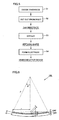
- FIG. 2 is a flow chart showing the method of manufacturing epitaxialwafer 20 according to this embodiment.
- t1 (m) represents the thickness of GaN substrate 10
- r (m) represents the radius of GaN substrate 10
- t2 (m) represents the thickness of Al x Ga (1-x) N layer 21
- h (m) represents the warp of epitaxialwafer 20
- a1 (m) represents the lattice constant of GaN
- a2 (m) represents the lattice constant of AlN
- the value t1 found by the following expression 1 is decided as the minimum thickness of GaN substrate 10, as shown in Fig.
- the aforementioned "lattice constant a1 of GaN” and “lattice constant a2 of AlN” denote those in a direction perpendicular to c-axes.
- GaN and AlN are hexagonal compounds. Hexagonal compounds have lattice constants a1 and a2 in the direction perpendicular to the c-axes and lattice constants c1 and c2 in the c-axis direction.
- the lattice constant a1 in the direction perpendicular to the c-axis is 3.19 ⁇ 10 -10 m(3.19 ⁇ )
- the lattice constant c1 in the c-axis direction is 5.19 ⁇ 10 -10 m(5.19 ⁇ ).
- the lattice constant a2 in the direction perpendicular to the c-axis is 3.11 ⁇ 10 -10 m(3.11 ⁇ ), and the lattice constant c2 in the c-axis direction is 4.98 ⁇ 10 -10 m(4.98 ⁇ ).
- the radius r of GaN substrate 10 is first obtained.
- This radius r may be obtained by preparing an ingot of GaN and measuring the length of a portion of this ingot for forming the radius r of GaN substrate 10. If the ingot includes an underlayer substrate and a layer of GaN formed on this underlayer substrate, the radius r may be obtained as the radius of the underlayer substrate, for example.
- the thickness t2 of manufactured epitaxialwafer 20, the warp h (see Fig. 7 ) of epitaxialwafer 20 and the composition x of Al constituting Al x Ga (1-x) N layer 21 are set.
- the warp h of epitaxialwafer 20 is set to a value allowing photolithography with a stepper or an aligner, for example.
- the lattice constants a1 and a2 of GaN and AlN are known values, as described above.
- the values r, t2, h, x, a1 and a2 are substituted in the expression 1, thereby finding the thickness t1 of GaN substrate 10. This thickness t 1 is regarded as the minimum thickness.
- the total thickness thereof is regarded as the thickness t2 of Al x Ga (1-x) N layers 21. If a plurality of Al x Ga (1-x) N layers 21 are provided, further, the Al composition in Al x Ga (1-x) N layer 21 most occupying the thickness t2 is regarded as the Al composition x.
- GaN substrate 10 having a thickness of at least the minimum thickness and less than 400 ⁇ m is cut out from the ingot of GaN (step S2).
- the thickness of GaN substrate 10 cut out from the prepared ingot is decided. Thereafter GaN substrates 10 are cut out from the ingot by slicing or the like, so that each GaN substrate 10 has this thickness.
- the method of cutting out GaN substrate 10 is not particularly restricted, but a well-known method can be employed.
- GaN substrate 10 cut out from the ingot preferably has a thickness of at least the minimum thickness decided in the above expression 1 and less than 400 ⁇ m, more preferably at least the minimum thickness, and at least 100 ⁇ m and less than 250 ⁇ m.
- GaN substrate 10 can be employed for epitaxialwafer 20 having the set warp h. If GaN substrate 10 having this minimum thickness is hard to handle, GaN substrate 10 is preferably cut out from the ingot with a thickness exceeding the minimum thickness and allowing handling. Particularly when having a thickness of at least 100 ⁇ m, cut-out GaN substrate 10 is easy to handle.
- cut-out GaN substrate 10 When having a thickness of less than 400 ⁇ m, cut-out GaN substrate 10 is extremely easy to handle. When GaN substrate 10 has a thickness of less than 250 ⁇ m, the number of cut-out GaN substrates 10 can be increased, and each GaN substrate 10 is easy to handle.
- GaN substrate 10 can be manufactured by carrying out the aforementioned steps. GaN substrate 10 manufactured in this manner may further be subjected to polishing or the like. In order to manufacture epitaxialwafer 20 shown in Fig. 1 , the following step is further carried out:
- Fig. 3 is a schematic sectional view showing an epitaxialwafer 30 according to a second embodiment of the present invention.
- epitaxialwafer 30 according to this embodiment comprises a GaN substrate 31, a buffer layer 32, an active layer 33, an electron blocking layer 34 and a contact layer 35.
- Fig. 4 is a schematic sectional view showing an LED 40 as a semiconductor device according to the second embodiment of the present invention.
- LED 40 serving as the semiconductor device according to the second embodiment comprises epitaxialwafer 30 shown in Fig. 3 and electrodes 41 and 42.
- GaN substrate 31 has a thickness t31.
- Buffer layer 32 is formed on the c-plane of GaN substrate 31.
- Buffer layer 32 is made of n-type GaN, for example, and has a thickness t32.
- Active layer 33 is formed on buffer layer 32.
- Active layer 33 has a thickness t33.
- Active layer 33 is constituted of a multiple quantum well structure consisting of InGaN and GaN, for example. Active layer 33 may alternatively consist of a single semiconductor material.
- Electron blocking layer 34 is formed on active layer 33.
- Electron blocking layer 34 is made of p-type Al x Ga (1-x) N, for example, and has a thickness t34.
- Contact layer 35 is formed on electron blocking layer 34.
- Contact layer 35 is made of p-type GaN, for example, and has a thickness t3 5.
- electrode 41 is formed on the surface of GaN substrate 31 opposite to that provided with buffer layer 32. Electrode 41 is made of titanium and aluminum, for example. Electrode 42 is formed on contact layer 35. Electrode 42 is made of nickel and gold, for example.
- Fig. 5 is a flow chart showing the method of manufacturing the semiconductor device according to this embodiment.
- the minimum thickness of GaN substrate 31 is decided through the above expression 1 (step S1).
- the thickness t2 and the Al composition x of the Al x Ga (1-x) N layer and the warp h of epitaxialwafer 30 in the expression 1 are set.
- GaN substrate 31 is employed for epitaxialwafer 30 shown in Fig. 3 , and hence the thickness t2 of the Al x Ga (1-x) N layer in the expression 1 corresponds to the thickness t34 of electron blocking layer 34.
- active layer 33 includes an Al x Ga (1-x) N layer
- the Al x Ga (1-x) N layer included in active layer 33 is extremely thin, and hence the sum of the thickness of the Al x Ga (1-x) N layer included in active layer 33 and the thickness t34 of electron blocking layer 34 is substantially equal to the thickness t34 of electron blocking layer 34.
- the Al composition x of the Al x Ga (1-x) N layer in the expression 1 corresponds to the Al composition x of electron blocking layer 34.
- electron blocking layer 34 most occupies the total thickness t2 of the Al x Ga (1-x) N layers, and hence the Al composition x of the Al x Ga (1-x) N layer in the expression 1 corresponds to the Al composition x of electron blocking layer 34.
- Epitaxialwafer 30 has an LED structure, and hence the warp h is set to not more than 100 ⁇ m, for example.
- the radius r of GaN substrate 31 is obtained. This radius r can be obtained by measuring the radius of an underlayer substrate employed for an ingot as described above, for example.
- the set values of the thickness t2 and the Al composition x of the Al x Ga (1-x) N layer and the warp h and the radius r of epitaxialwafer 30 are substituted in the expression 1, thereby finding the minimum thickness t1 of GaN substrate 31.
- GaN substrate 31 having a thickness of at least the minimum thickness and less than 400 ⁇ m is cut out from an ingot of GaN (step S2). If GaN substrate 31 having the minimum thickness t 1 found from the expression 1 is hard to handle, the thickness of GaN substrate 31 is changed to that of not more than 400 ⁇ m allowing easy handling. If GaN substrate 31 is employed for epitaxialwafer 30 having the LED structure, the thickness of GaN substrate 31 is preferably set to at least the minimum thickness and less than 250 ⁇ m. GaN substrate 31 is thus cut out from the ingot with the decided thickness.
- buffer layer 32 is formed on the c-plane of GaN substrate 31.
- active layer 33 is formed on buffer layer 32.
- electron blocking layer 34 is formed on active layer 33.
- contact layer 35 is formed on electron blocking layer 34.
- These epitaxial layers can be unrestrictedly formed by HVPE or MOCVD, for example.
- Epitaxialwafer 30 shown in Fig. 3 is manufactured by carrying out the aforementioned steps.
- step (S4) is further carried out: Electrode 41 is formed on a surface of GaN substrate 31 opposite to that provided with buffer layer 32. Further, electrode 42 is formed on contact layer 35. The method of forming electrodes 41 and 42 is not particularly restricted.
- Masks are formed on the surface and the back surface of epitaxialwafer 30 by photolithography, for example, metal layers for preparing electrodes 41 and 42 are formed by vapor deposition, for example, and electrodes 41 and 42 are formed by lift-off, for example.
- LED 40 shown in Fig. 4 is manufactured by carrying out the aforementioned steps.
- the remaining structure of the second embodiment is similar to that of the aforementioned first embodiment, and hence redundant description is not repeated.
- Example of the present invention is now described.
- the relation between the thickness t 1 of GaN substrate 10 and the warp h of epitaxialwafer 20 was examined in order to find out the expression 1 for deciding the minimum thickness of GaN substrate 10 employed for epitaxialwafer 20 having at least three layers, i.e., GaN substrate 10, Al x Ga (1-x) N layer 21 formed on the c-plane of GaN substrate 10 and GaN layer 22 formed on Al x Ga (1-x) N layer 21, as shown in Fig. 1 .
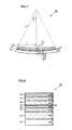
- Fig. 6 is a schematic sectional view showing an epitaxialwafer 100 consisting of a GaN substrate 10 and an Al x Ga (1-x) N layer 21 formed on GaN substrate 10.
- epitaxialwafer 100 having a two-layer structure consisting of GaN substrate 10 and Al x Ga (1-x) N layer 21 formed on the c-plane of GaN substrate 10 as shown in Fig. 6 the lattice constants of GaN and Al x Ga (1-x) N are different from each other, and hence it is known that epitaxialwafer 100 of the two-layer structure is strained.
- the lattice constant of Al x Ga (1-x) N is smaller than that of GaN, and hence tensile stress is applied to the side of Al x Ga (1-x) N layer 21 while compressive stress is applied to the side of GaN substrate 10. Consequently, epitaxialwafer 100 has a downwardly convexed warp, as shown in Fig. 6 .
- the relation between the thickness of GaN substrate 10 and the warp of epitaxialwafer 100 having the two-layer structure is now described with reference to Fig. 6 . It is assumed that Al x Ga (1-x) N layer 21 is coherently grown on GaN substrate 10 with a thickness allowing no lattice relaxation.
- Fig. 7 is a schematic sectional view showing a warped state of epitaxialwafer 20 having three layers. In other words, Fig. 7 shows a warped state of epitaxialwafer 20 shown in Fig. 1 .
- the layer (GaN layer 22 in Figs. 1 and 7 ) formed on Al x Ga (1-x) N layer 21 has an extremely small thickness as compared with GaN substrate 10 in epitaxialwafer 20 having at least three layers, and hence the inventors have considered correcting the expression 8 applied to epitaxialwafer 100 having the two-layer structure and applying the corrected expression to epitaxialwafer 20 having at least three layers.
- GaN layer 22 is formed on Al x Ga (1-x) N layer 21 in epitaxialwafer 20 having at least three layers, and hence Al x Ga (1-x) N layer 21 is strained due to GaN substrate 10 and GaN layer 22 respectively.
- epitaxialwafer 100 having the two-layer structure on the other hand, only one surface is strained. Therefore, the inventors have considered that the Young's modulus E2 of Al x Ga (1-x) N layer 21 in the expression 8 applied to epitaxialwafer 100 having the two-layer structure cannot be applied to epitaxialwafer 20 having at least three layers. Hence, the inventors have considered substituting another constant E for the Young's modulus E2 in the expression 8.
- the proportionality factor k in the expression 8 is proportionate to the difference between the lattice constants of GaN and Al x Ga (1-x) N on the interface between GaN substrate 10 and Al x Ga (1-x) N layer 21. Therefore, the inventors have considered that the proportionality factor k set only in consideration of the difference between the lattice constants of GaN and Al x Ga (1-x) N cannot be applied to epitaxialwafer 20 having at least three layers if GaN layer 22 is formed on Al x Ga (1-x) N layer 21 in epitaxialwafer 20 having at least three layers. Thus, the inventors have considered substituting another constant K for the proportionality factor k in the expression 8.
- the Al composition x and the thickness of Al x Ga (1-x) N layer 21 were set to over zero and not more than 0.3 and over zero and not more than 30 nm respectively.
- E2 and k are constants depending on the Al composition x of Al x Ga (1-x) N layer 21. If the Al composition x is over zero and not more than 1 and the thickness is unlimited in Al x Ga (1-x) N layer 21 of epitaxialwafer 20, fluctuation ranges of the constants E and K are increased.
- the Al composition x and the thickness were set to over zero and not more than 0.3 and over zero and not more than 30 nm respectively in Al x Ga (1-x) N layer 21 of epitaxialwafer 20 in this Example.
- the inventors have manufactured seven samples 1 to 7 of epitaxialwafer 30 constituting LED 40 shown in Fig. 4 and measured the relation between the thickness of GaN substrate 10 and the warp of epitaxialwafer 30 in each sample, in order to decide the values of the constants E and K in the expression 12.
- GaN substrate 31 having a thickness t31 of 350 ⁇ m and a radius r of 25 mm was prepared for the sample 1 of epitaxialwafer 30 having the LED structure shown in Fig. 3 .
- buffer layer 32 of n-type GaN having a thickness t32 of 2.0 ⁇ m was formed on GaN substrate 31 by MOCVD.
- active layer 33 having a 3QW (quantum well) structure of InGaN/GaN with a thickness t33 of 0.05 ⁇ m was formed on buffer layer 32 by MOCVD.
- electron blocking layer 34 of Al 0.18 Ga 0.82 N having a thickness t34 of 0.02 ⁇ m was formed on active layer 33 by MOCVD.
- contact layer 35 of p-type GaN having a thickness t35 of 0.2 ⁇ m was formed on electron blocking layer 34 by MOCVD.
- the sample 2 of epitaxialwafer 30 was basically similar in structure to the sample 1, except that the thickness t31 of GaN substrate 31 was set to 250 ⁇ m.
- the sample 3 of epitaxialwafer 30 was basically similar in structure to the sample 1, except that the thickness t31 of GaN substrate 31 was set to 200 ⁇ m.
- the sample 4 of epitaxialwafer 30 was basically similar in structure to the sample 1, except that the Al composition x and the thickness of the Al x Ga (1-x) N layer were set to 0.30 and 0.03 ⁇ m respectively.
- the sample 5 of epitaxialwafer 30 was basically similar in structure to the sample 1, except that the Al composition x and the thickness of the Al x Ga (1-x) N layer were set to 0.30 and 0.03 ⁇ m respectively and the thickness t31 of GaN substrate 31 was set to 250 ⁇ m.
- the sample 6 of epitaxialwafer 30 was basically similar in structure to the sample 1, except that the Al composition x and the thickness of the Al x Ga (1-x) N layer were set to 0.30 and 0.03 ⁇ m respectively and the thickness t31 of GaN substrate 31 was set to 200 ⁇ m.
- the sample 7 of epitaxialwafer 30 was basically similar in structure to the sample 1, except that the Al composition x and the thickness of the Al x Ga (1-x) N layer were set to 0.30 and 0.03 ⁇ m respectively and the thickness t31 of GaN substrate 31 was set to 150 ⁇ m.
- FIG. 8 is a schematic sectional view showing each of the samples 8 and 9 of epitaxialwafers. More specifically, a GaN substrate 51 having a thickness t51 of 400 ⁇ m and a radius of 25 mm was prepared.
- the thickness t1 of GaN substrate 10 was so set as to satisfy the warp h of epitaxialwafer 30, and the constants E and K were obtained by least squares approximation. Consequently, it has been found that the constants E and K are equal to 1.2 ⁇ 10 11 and 1.33 respectively.
- the Young's modulus E1 was set to that of GaN, i.e., 1.5 ⁇ 10 11 (GPa).
- the expression 1 related to the epitaxialwafer having at least three layers according to the present invention and the expressions 8 and 11 related to epitaxialwafer 100 having the two-layer structure are compared with each other with reference to Fig. 9 .
- Fig. 9 shows the relations between the thicknesses t1 of GaN substrates and warps h of epitaxialwafers as to the expression 1 according to the present invention, expressions derived from the expressions 8 and 11 related to epitaxialwafer 100 having the two-layer structure and the samples 1 to 9.
- "inventive expression 1" denotes the warps h (m) of epitaxialwafers with the Al composition x of 0.18 in the above expression 1.
- Conventional expression 1 denotes the warps h of epitaxialwafers with the Al composition x of 0.18, the Young's modulus E2 of Al 0.18 Ga 0.82 N of 1.78 ⁇ 10 11 (GPa) and the proportionality factor k of epitaxialwafer 100 having the two-layer structure of 1.00 in the above expressions 8 and 11.
- Conventional expression 2 denotes the warps h of epitaxialwafers with the Al composition x of 0.30, the Young's modulus E2 of Al 0.30 Ga 0.70 N of 1.97 ⁇ 10 11 (GPa) and the proportionality factor k of Al 0.30 Ga 0.70 N of 1.00 in the above expressions 8 and 11.
- the Young's moduli E1 in the inventive expression 1 and the conventional expressions 1 and 2 were set to that of GaN, i.e., 1.5 ⁇ 10 11 .
- the expression 1 found by assuming the expression 12 and examining the constants E and K is applicable to epitaxialwafer 20 having at least three layers in the aforementioned structure.
- the thickness t1 (200 ⁇ m, for example) of the GaN substrate in the case of setting the warp h (6 ⁇ m, for example) of the epitaxialwafer in the expression (conventional expression 1 in Fig. 9 ) for epitaxialwafer 100 having the two-layer structure with the Al composition x of 0.18 was smaller than the thickness (250 ⁇ m, for example) of GaN substrate 31 according to each of the samples 1 and 2 with the Al composition x of 0.18 satisfying the same warp h (6 ⁇ m, for example) of epitaxialwafer 30.
- epitaxialwafer 100 manufactured with GaN substrate 10 having the thickness found through the expression for epitaxialwafer 100 having the two-layer structure may not satisfy the performance of the warp h, and hence it has been recognized that the conventional expression 1 cannot be applied to epitaxialwafer 20 having at least three layers including GaN substrate 10, Al x Ga (1-x) N layer 21 and GaN layer 22.
- the thickness t1 of GaN substrate 10 in the case of setting the warp h of epitaxialwafer 100 in the expression for epitaxialwafer 100 having the two-layer structure was larger than that of GaN substrate 10 according to each of the samples 4 to 7 satisfying the same warp h of epitaxialwafer 20 with the Al composition x of 0.30.
- the thickness of epitaxialwafer 100 prepared by setting the warp h, the thickness t2 and the Al composition x thereof in the expression for epitaxialwafer 100 having the two-layer structure with the Al composition x of 0.30, manufacturing GaN substrate 10 with the thickness found by substituting the Young's modulus of Al x Ga (1-x) N in the expression and forming Al x Ga (1-x) N layer 21 and GaN layer 22 thereon was larger than the thickness t1 of GaN substrate 10 obtained through the inventive expression 1.
- the thickness t 1 of GaN substrate 10 found through the expression for epitaxialwafer 100 having the two-layer structure with the Al composition x of 0.30 is not optimum for satisfying the set warp h of epitaxialwafer 20.
- the expression for finding the minimum thickness of GaN substrate 10 for satisfying the warp h of epitaxialwafer 20 having at least three layers was found out. Further, it was possible to confirm that the minimum thickness satisfying the set warp h of epitaxialwafer 20 can be decided according to the expression 1.
- the present invention is particularly advantageously applicable to a method of manufacturing a GaN substrate having a c-plane for manufacturing an epitaxialwafer by successively stacking an Al x Ga (1-x) N layer and a GaN layer on the c-plane.
Landscapes
- Chemical & Material Sciences (AREA)
- Engineering & Computer Science (AREA)
- Crystallography & Structural Chemistry (AREA)
- Materials Engineering (AREA)
- Metallurgy (AREA)
- Organic Chemistry (AREA)
- Inorganic Chemistry (AREA)
- Chemical Kinetics & Catalysis (AREA)
- General Chemical & Material Sciences (AREA)
- Crystals, And After-Treatments Of Crystals (AREA)
- Led Devices (AREA)
- Recrystallisation Techniques (AREA)
Abstract

A GaN substrate (10) having a thickness of at least this minimum thickness (tl) and less than 400 µm is formed.
Description
- The present invention relates to a method of manufacturing a GaN substrate, a method of manufacturing an epitaxialwafer, a method of manufacturing a semiconductor device and an epitaxialwafer, and more particularly, it relates to a method of manufacturing a GaN substrate having a c-plane for manufacturing an epitaxialwafer by successively stacking at least two layers including an AlxGa(1-x)N layer and a GaN layer on the c-plane, a method of manufacturing an epitaxialwafer, a method of manufacturing a semiconductor device and an epitaxialwafer.
- In general, a GaN (gallium nitride) substrate is employed as the substrate for a semiconductor device such as a light-emitting diode (LED) or a laser diode (LD). When GaN having an energy band gap of 3.4 eV and high thermal conductivity is applied to the substrate for the semiconductor device, an electrode can be provided on the back surface of the GaN substrate, and the driving (operating) voltage of the semiconductor device can be reduced.
- Such a GaN substrate is manufactured by a method described in K. Motoki et al., "Preparation of Large GaN Substrates", Materials Science and Engineering B93 (2002), pp. 123 - 125, for example. This document discloses that the GaN substrate is manufactured through the following steps: First, a buffer layer of GaN having a thickness of 60 µm is formed on a GaAs (gallium arsenide) substrate by HVPE (Hydride Vapor Phase Epitaxy). Thereafter a GaN layer having a thickness of 500 µm is formed on the buffer layer by HVPE. Thereafter the GaAs substrate is removed, and a GaN substrate having a thickness of 495 ± 10 µm is obtained by polishing.
- According to the aforementioned document, however, no plurality of GaN substrates are cut out from a bulk GaN single crystal in the thickness direction, and hence a high cost is disadvantageously required for obtaining the GaN substrate.
- In order to reduce the cost for each GaN substrate, a technique of manufacturing a GaN substrate by manufacturing an ingot of GaN having a large thickness and cutting out a plurality of GaN substrates from this ingot in the thickness direction is conceivable. If the GaN substrate cut out from the ingot has a thickness of 495 ± 10 µm as described in the aforementioned document, however, this thickness may be excessive, depending on the performance of a warp required to the semiconductor device formed on this GaN substrate. In this case, the cost cannot be sufficiently reduced.
- While the GaN substrate is preferably cut out from the ingot with a smaller thickness in order to further reduce the cost, the GaN substrate having a small thickness may be cracked when subjected to working such as polishing. Even if the GaN substrate remains uncracked, an epitaxialwafer comprising the GaN substrate and epitaxial layers may be remarkably warped when the epitaxial layers are formed on the GaN substrate. In this case, photolithography or the like cannot be performed in order to form an electrode on this epitaxialwafer, and the epitaxialwafer cannot be applied to a semiconductor device.
- Accordingly, an object of the present invention is to provide a method of manufacturing a GaN substrate allowing formation of an epitaxialwafer with a warp of not more than a required level and enabling reduction of the cost, a method of manufacturing an epitaxialwafer, a method of manufacturing a semiconductor device and an epitaxialwafer.
- The method of manufacturing a GaN substrate according to the present invention is a method of manufacturing a GaN substrate having a c-plane for manufacturing an epitaxialwafer by successively stacking at least two layers including an AlxGa(1-x)N layer having an Al composition x of over zero and not more than 0.3 and a thickness of over zero and not more than 30 nm and a GaN layer on the c-plane through the following steps: Assuming that t1 (m) represents the thickness of the GaN substrate, r (m) represents the radius of the GaN substrate, t2 represents the thickness of the AlxGa(1-x)N layer, x represents the Al composition in the AlxGa(1-x)N layer, h (m) represents a warp of the epitaxialwafer, a1 represents the lattice constant of GaN and a2 represents the lattice constant of AlN, the value t1 found by the
following expression 1 is decided as the minimum thickness of the GaN substrate:
- Then, a GaN substrate having a thickness of at least this minimum thickness and less than 400 µm is cut out from an ingot of GaN.
- The inventors have deeply studied a method of deciding the thickness of the GaN substrate employed for the epitaxialwafer having the aforementioned structure, to find the
above expression 1. In other words, the minimum thickness for satisfying the set warp h of the epitaxialwafer can be decided by theabove expression 1, and hence the number of GaN substrates obtained in the thickness direction can be increased by cutting out each GaN substrate from one ingot with the thickness of at least the decided minimum thickness and less than 400 µm. Therefore, a GaN substrate capable of reducing the warp of the formed epitaxialwafer to not more than the required level and attaining reduction of the cost can be manufactured. - In a case of manufacturing a GaN substrate employed for an epitaxialwafer comprising a plurality of AlxGa(1-x)N layers, t2 represents the total thickness of the plurality of AlxGa(1-x)N layers. In this case, further, x represents the Al composition ratio in the AlxGa(1-x)N layer most occupying the total thickness t2. The Al composition x is expressed in a molar ratio.
- Preferably in the aforementioned method of manufacturing a GaN substrate, a GaN substrate having a thickness, at least the minimum thickness, of at least 100 µm and less than 250 µm is formed in the aforementioned step of cutting out the GaN substrate.
- When the minimum thickness is less than 100 µm, the thickness of the GaN substrate is so set to at least 100 µm that the GaN substrate is easy to handle and the number of the GaN substrate manufacturable from one ingot in the thickness direction can be increased. When the minimum thickness is less than 100 µm, further, the thickness of the GaN substrate is so set to less than 250 µm that the more easily handleable GaN substrate can be manufactured.
- In a method of manufacturing an epitaxialwafer according to an aspect of the present invention, the following steps are carried out: First, the aforementioned GaN substrate is manufactured by the aforementioned method of manufacturing a GaN substrate. An AlxGa(1-x)N layer is formed on the c-plane of this GaN substrate. A GaN layer is formed on this AlxGa(1-x)N layer.
- According to the method of manufacturing an epitaxialwafer according to this aspect of the present invention, an epitaxialwafer having a warp of not more than h and comprising a GaN substrate having a small thickness can be manufactured, even if the AlxGa(1-x)N layer and the GaN layer are formed on the GaN substrate. Therefore, the manufactured epitaxialwafer can be applied to a semiconductor device, and the epitaxialwafer can be manufactured at a cost reduced due to the reduction of the cost for manufacturing the GaN substrate.
- In a method of manufacturing an epitaxialwafer according to another aspect of the present invention, the following steps are carried out: First, the aforementioned GaN substrate is manufactured by the aforementioned method of manufacturing a GaN substrate. A GaN layer is formed on the c-plane of this GaN substrate. An AlxGa(1-x)N layer is formed on this GaN layer. Another GaN layer is formed on this AlxGa(1-x)N layer.
- According to the method of manufacturing an epitaxialwafer according to this aspect of the present invention, an epitaxialwafer having a warp of not more than h and comprising a GaN substrate having a small thickness can be manufactured even if the GaN layer, the AlxGa(1-x)N layer and the GaN layer are formed on the GaN substrate in this order. Therefore, the manufactured epitaxialwafer can be applied to a semiconductor device, and the epitaxialwafer can be manufactured at a cost reduced due to the reduction of the cost for manufacturing the GaN substrate.
- In the method of manufacturing a semiconductor device according to the present invention, the following steps are carried out: First, an epitaxialwafer is manufactured by the aforementioned method of manufacturing an epitaxialwafer. Then, an electrode is formed on the epitaxialwafer.
- According to the method of manufacturing a semiconductor device according to the present invention, an epitaxialwafer having a warp of not more than h and comprising a GaN substrate having a small thickness can be manufactured even if the electrode is formed on the epitaxialwafer. Therefore, the semiconductor device can be manufactured at a cost reduced due to the reduction of the cost for manufacturing the GaN substrate.
- The epitaxialwafer according to the present invention comprises a GaN substrate, an AlxGa(1-x)N layer formed on the c-plane of the GaN substrate and a GaN layer formed on the AlxGa(1-x)N layer. The thickness of the GaN substrate is less than 250 µm. A warp of the epitaxialwafer is not more than 100 µm.
- According to the epitaxialwafer according to the present invention, the thickness of the GaN substrate can be reduced to the conventionally unattainable level of less than 250 µm through the
above expression 1, and the warp of the epitaxialwafer can be reduced to not more than 100 µm. - According to the method of manufacturing a GaN substrate, the method of manufacturing an epitaxialwafer, the method of manufacturing a semiconductor device and the epitaxialwafer according to the present invention, the warp of the formed epitaxialwafer is reduced to not more than the required level, and the cost for the GaN substrate can be reduced.
- The foregoing and other objects, features, aspects and advantages of the present invention will become more apparent from the following detailed description of the present invention when taken in conjunction with the accompanying drawings.
-
-
Fig. 1 is a schematic sectional view showing an epitaxialwafer according to a first embodiment of the present invention; -
Fig. 2 is a flow chart showing a method of manufacturing the epitaxialwafer according to the first embodiment of the present invention; -
Fig. 3 is a schematic sectional view showing an epitaxialwafer according to a second embodiment of the present invention; -
Fig. 4 is a schematic sectional view showing a semiconductor device according to the second embodiment of the present invention; -
Fig. 5 is a flow chart showing a method of manufacturing the semiconductor device according to the second embodiment; -
Fig. 6 is a schematic sectional view showing an epitaxialwafer consisting of a GaN substrate and an AlxGa(1-x)N layer formed on the GaN substrate; -
Fig. 7 is a schematic sectional view showing a warped state of an epitaxialwafer having three layers; -
Fig. 8 is a schematic sectional view showing each of samples 8 and 9 of epitaxialwafers; and -
Fig. 9 shows the relations between thicknesses t1 of GaN substrates and warps h of epitaxialwafers as to theexpression 1 according to the present invention, expressions as to an epitaxialwafer having two layers andsamples 1 to 9. - Embodiments of the present invention are now described with reference to the drawings. In the accompanying drawings, portions identical or corresponding to each other are denoted by the same reference numerals, and redundant description is not repeated.
-
Fig. 1 is a schematic sectional view showing anepitaxialwafer 20 according to a first embodiment of the present invention. As shown inFig. 1 ,epitaxialwafer 20 comprises aGaN substrate 10, an AlxGa(1-x)N layer 21 and aGaN layer 22.GaN substrate 10 has a c-plane. AlxGa(1-x)N layer 21 is formed on the c-plane ofGaN substrate 10.GaN layer 22 is formed on AlxGa(1-x)N layer 21. - The thickness t1 of
GaN substrate 10 is less than 250 µm, and a warp ofepitaxialwafer 20 is not more than 100 µm. More preferably, thethickness t 1 ofGaN substrate 10 is at least 100 µm and less than 250 µm, and the warp ofepitaxialwafer 20 is at least 2 µm and not more than 85 µm. Particularly preferably, the thickness t1 ofGaN substrate 10 is at least 120 µm and not more than 240 µm, and the warp ofepitaxialwafer 20 is at least 2 µm and not more than 50 µm. When the thickness t1 ofGaN substrate 10 and the warp ofepitaxialwafer 20 are in these ranges respectively, the performance of a warp necessary for an LED is satisfied, and the thickness t1 ofGaN substrate 10 is small. When the warp ofepitaxialwafer 20 is 12 µm, the maximum thickness t1 ofGaN substrate 10 calculated from theabove expression 1 is 250 µm. When the warp ofepitaxialwafer 20 is 50 µm, on the other hand, themaximum thickness t 1 ofGaN substrate 10 calculated from theabove expression 1 is 120 µm. In other words, thethickness t 1 ofGaN substrate 10 and the warp ofepitaxialwafer 20 satisfy the relation of not more than the warp h ofepitaxialwafer 20 set in theabove expression 1. - If
GaN substrate 10 is warped, the thickness t1 corresponds to that ofGaN substrate 10 in virtual lines extended from lines along side surfaces including both ends of an arbitrary radius ofGaN substrate 10. - The Al composition x in AlxGa(1-x)N layer 21, not particularly restricted so far as the same is over zero and not more than 0.30, is preferably at least 0.05 and not more than 0.30, more preferably at least 0.18 and not more than 0.30. In this case,
epitaxialwafer 20 is suitably applied to a semiconductor device. - The thickness t2 of AlxGa(1-x)N layer 21, not particularly restricted so far as the same is over zero and not more than 30 nm, is preferably at least 10 nm and not more than 30 nm, more preferably at least 20 nm and not more than 30 nm. In this case,
epitaxialwafer 20 is suitably applied to a semiconductor device. - If
epitaxialwafer 20 is warped, the thickness t2 of AlxGa(1-x)N layer 21 corresponds to that ofepitaxialwafer 20 in virtual lines extended from lines along side surfaces including both ends of an arbitrary radius ofepitaxialwafer 20. - A plurality of AlxGa(1-x)N layers 21 may be provided, and GaN layer may be provided between AlxGa(1-x)N layers 21. If a plurality of AlxGa(1-x)N layers 21 are provided, the total thickness thereof is regarded as the thickness t2 of AlxGa(1-x)N layers 21. If a plurality of AlxGa(1-x)N layers 21 are provided, further, the Al composition in AlxGa(1-x)N layer 21 most occupying the thickness t2 is regarded as the Al composition X.
- The thickness t3 of
GaN layer 22 is smaller than the thickness t1 ofGaN substrate 10. A plurality of GaN layers 22 may be provided, and another AlxGa(1-x)N layer may further be provided between GaN layers. - The radius r (see
Fig. 7 ) ofGaN substrate 10 is preferably at least 25 nm. If the radius r is at least 25 nm, a mass production process can be carried out at a proper cost. - A method of
manufacturing epitaxialwafer 20 according to this embodiment is described with reference toFigs. 1 and 2. Fig. 2 is a flow chart showing the method ofmanufacturing epitaxialwafer 20 according to this embodiment. - Assuming that t1 (m) represents the thickness of
GaN substrate 10, r (m) represents the radius ofGaN substrate 10, t2 (m) represents the thickness of AlxGa(1-x)N layer 21, h (m) represents the warp ofepitaxialwafer 20, a1 (m) represents the lattice constant of GaN and a2 (m) represents the lattice constant of AlN, the value t1 found by the followingexpression 1 is decided as the minimum thickness ofGaN substrate 10, as shown inFig. 2 (step S1):
- The aforementioned "lattice constant a1 of GaN" and "lattice constant a2 of AlN" denote those in a direction perpendicular to c-axes. GaN and AlN are hexagonal compounds. Hexagonal compounds have lattice constants a1 and a2 in the direction perpendicular to the c-axes and lattice constants c1 and c2 in the c-axis direction. As to GaN, the lattice constant a1 in the direction perpendicular to the c-axis is 3.19×10⁻¹⁰m(3.19Å), and the lattice constant c1 in the c-axis direction is 5.19×10⁻¹⁰m(5.19Å). As to AlN, the lattice constant a2 in the direction perpendicular to the c-axis is 3.11×10⁻¹⁰m(3.11Å), and the lattice constant c2 in the c-axis direction is 4.98×10⁻¹⁰m(4.98Å).
- More specifically, the radius r of
GaN substrate 10 is first obtained. This radius r may be obtained by preparing an ingot of GaN and measuring the length of a portion of this ingot for forming the radius r ofGaN substrate 10. If the ingot includes an underlayer substrate and a layer of GaN formed on this underlayer substrate, the radius r may be obtained as the radius of the underlayer substrate, for example. - Then, the thickness t2 of manufactured
epitaxialwafer 20, the warp h (seeFig. 7 ) ofepitaxialwafer 20 and the composition x of Al constituting AlxGa(1-x)N layer 21 are set. The warp h ofepitaxialwafer 20 is set to a value allowing photolithography with a stepper or an aligner, for example. The lattice constants a1 and a2 of GaN and AlN are known values, as described above. The values r, t2, h, x, a1 and a2 are substituted in theexpression 1, thereby finding the thickness t1 ofGaN substrate 10. Thisthickness t 1 is regarded as the minimum thickness. - If a plurality of AlxGa(1-x)N layers 21 are provided, the total thickness thereof is regarded as the thickness t2 of AlxGa(1-x)N layers 21. If a plurality of AlxGa(1-x)N layers 21 are provided, further, the Al composition in AlxGa(1-x)N layer 21 most occupying the thickness t2 is regarded as the Al composition x.
- Then,
GaN substrate 10 having a thickness of at least the minimum thickness and less than 400 µm is cut out from the ingot of GaN (step S2). - More specifically, the thickness of
GaN substrate 10 cut out from the prepared ingot is decided. ThereafterGaN substrates 10 are cut out from the ingot by slicing or the like, so that eachGaN substrate 10 has this thickness. The method of cutting outGaN substrate 10 is not particularly restricted, but a well-known method can be employed. -
GaN substrate 10 cut out from the ingot preferably has a thickness of at least the minimum thickness decided in theabove expression 1 and less than 400 µm, more preferably at least the minimum thickness, and at least 100 µm and less than 250 µm. When cut out from the ingot with the minimum thickness decided in theabove expression 1,GaN substrate 10 can be employed forepitaxialwafer 20 having the set warp h. IfGaN substrate 10 having this minimum thickness is hard to handle,GaN substrate 10 is preferably cut out from the ingot with a thickness exceeding the minimum thickness and allowing handling. Particularly when having a thickness of at least 100 µm, cut-outGaN substrate 10 is easy to handle. When having a thickness of less than 400 µm, cut-outGaN substrate 10 is extremely easy to handle. WhenGaN substrate 10 has a thickness of less than 250 µm, the number of cut-outGaN substrates 10 can be increased, and eachGaN substrate 10 is easy to handle. -
GaN substrate 10 can be manufactured by carrying out the aforementioned steps.GaN substrate 10 manufactured in this manner may further be subjected to polishing or the like. In order to manufactureepitaxialwafer 20 shown inFig. 1 , the following step is further carried out: - AlxGa(1-x)N layer 21 is formed on the c-plane of
GaN substrate 10, andGaN layer 22 is formed on AlxGa(1-x)N layer 21 (step S3). In this step 3, AlxGa(1-x)N layer 21 andGaN layer 22 are formed by epitaxy. This epitaxy is not particularly restricted, but vapor phase growth such as sublimation, HVPE, MBE (Molecular Beam Epitaxy) or MOCVD (Metal Organic Chemical Vapor Deposition) or liquid phase growth can be employed, for example. - In the step S3, AlxGa(1-x)N layer 21 is so formed that the Al composition x is over zero and not more than 0.3 and the thickness is over zero and not more than 30 nm. The
above expression 1 is set on the assumption that the warp h is maximized when the Al composition x and the thickness t1 ofGaN substrate 10 are in these ranges respectively. When the Al composition x and the thickness t1 ofGaN substrate 10 are in these ranges respectively, therefore, the set warp h ofepitaxialwafer 20 is satisfied, and the thickness t1 ofGaN substrate 10 for satisfying the warp h ofepitaxialwafer 20 is not excessively increased. Therefore, theabove expression 1 can be applied toepitaxialwafer 20 includingGaN substrate 10 having the Al composition x and the thickness t1 in the aforementioned ranges. - When a plurality of AlxGa(1-x)N layers 21 are provided, AlxGa(1-x)N layers 21 are so formed that the total thickness thereof regarded as the thickness t2 is over zero and not more than 30 nm and the Al composition x in AlxGa(1-x)N layer 21 most occupying the thickness t2 is over zero and not more than 0.3.
-
Epitaxialwafer 20 shown inFig. 1 is manufactured by carrying out the aforementioned steps. Afterepitaxialwafer 20 is manufactured, the surface ofGaN substrate 10 opposite to that provided with AlxGa(1-x)N layer 21 may further be subjected to polishing or the like.Epitaxialwafer 20 manufactured in this manner satisfies the warp h set before the manufacturing, andGaN substrate 10 has the minimum thickness in the range allowing handling. Thus, the cost for manufacturingGaN substrate 10 is reduced, whereby the cost for manufacturingepitaxialwafer 20 can also be reduced. -
Fig. 3 is a schematic sectional view showing anepitaxialwafer 30 according to a second embodiment of the present invention. As shown inFig. 3 ,epitaxialwafer 30 according to this embodiment comprises aGaN substrate 31, abuffer layer 32, anactive layer 33, anelectron blocking layer 34 and acontact layer 35.
Fig. 4 is a schematic sectional view showing anLED 40 as a semiconductor device according to the second embodiment of the present invention.LED 40 serving as the semiconductor device according to the second embodiment comprisesepitaxialwafer 30 shown inFig. 3 andelectrodes - In
epitaxialwafer 30 andLED 40,GaN substrate 31 has a thickness t31.Buffer layer 32 is formed on the c-plane ofGaN substrate 31.Buffer layer 32 is made of n-type GaN, for example, and has a thickness t32.Active layer 33 is formed onbuffer layer 32.Active layer 33 has a thickness t33.Active layer 33 is constituted of a multiple quantum well structure consisting of InGaN and GaN, for example.Active layer 33 may alternatively consist of a single semiconductor material.Electron blocking layer 34 is formed onactive layer 33.Electron blocking layer 34 is made of p-type AlxGa(1-x)N, for example, and has a thickness t34.Contact layer 35 is formed onelectron blocking layer 34.Contact layer 35 is made of p-type GaN, for example, and has a thickness t3 5. - In
LED 40,electrode 41 is formed on the surface ofGaN substrate 31 opposite to that provided withbuffer layer 32.Electrode 41 is made of titanium and aluminum, for example.Electrode 42 is formed oncontact layer 35.Electrode 42 is made of nickel and gold, for example. - Methods of manufacturing
GaN substrate 31,epitaxialwafer 30 andLED 40 according to this embodiment are now described with reference toFigs. 3 to 5 .Fig. 5 is a flow chart showing the method of manufacturing the semiconductor device according to this embodiment. - First, the minimum thickness of
GaN substrate 31 is decided through the above expression 1 (step S1). In order to decide the minimum thickness, the thickness t2 and the Al composition x of the AlxGa(1-x)N layer and the warp h ofepitaxialwafer 30 in theexpression 1 are set. - According to this embodiment,
GaN substrate 31 is employed forepitaxialwafer 30 shown inFig. 3 , and hence the thickness t2 of the AlxGa(1-x)N layer in theexpression 1 corresponds to the thickness t34 ofelectron blocking layer 34. Ifactive layer 33 includes an AlxGa(1-x)N layer, the AlxGa(1-x)N layer included inactive layer 33 is extremely thin, and hence the sum of the thickness of the AlxGa(1-x)N layer included inactive layer 33 and the thickness t34 ofelectron blocking layer 34 is substantially equal to the thickness t34 ofelectron blocking layer 34. - Further, the Al composition x of the AlxGa(1-x)N layer in the
expression 1 corresponds to the Al composition x ofelectron blocking layer 34. Also whenactive layer 33 includes the AlxGa(1-x)N layer,electron blocking layer 34 most occupies the total thickness t2 of the AlxGa(1-x)N layers, and hence the Al composition x of the AlxGa(1-x)N layer in theexpression 1 corresponds to the Al composition x ofelectron blocking layer 34. - Then, the warp h required to manufactured
epitaxialwafer 30 is set.Epitaxialwafer 30 has an LED structure, and hence the warp h is set to not more than 100 µm, for example. - Further, the radius r of
GaN substrate 31 is obtained. This radius r can be obtained by measuring the radius of an underlayer substrate employed for an ingot as described above, for example. - The set values of the thickness t2 and the Al composition x of the AlxGa(1-x)N layer and the warp h and the radius r of
epitaxialwafer 30 are substituted in theexpression 1, thereby finding the minimum thickness t1 ofGaN substrate 31. - Then,
GaN substrate 31 having a thickness of at least the minimum thickness and less than 400 µm is cut out from an ingot of GaN (step S2). IfGaN substrate 31 having theminimum thickness t 1 found from theexpression 1 is hard to handle, the thickness ofGaN substrate 31 is changed to that of not more than 400 µm allowing easy handling. IfGaN substrate 31 is employed forepitaxialwafer 30 having the LED structure, the thickness ofGaN substrate 31 is preferably set to at least the minimum thickness and less than 250 µm.GaN substrate 31 is thus cut out from the ingot with the decided thickness. - Then,
buffer layer 32 is formed on the c-plane ofGaN substrate 31. Then,active layer 33 is formed onbuffer layer 32. Then,electron blocking layer 34 is formed onactive layer 33. Then,contact layer 35 is formed onelectron blocking layer 34. These epitaxial layers can be unrestrictedly formed by HVPE or MOCVD, for example.Epitaxialwafer 30 shown inFig. 3 is manufactured by carrying out the aforementioned steps. In order to manufactureLED 40, the following step (S4) is further carried out:Electrode 41 is formed on a surface ofGaN substrate 31 opposite to that provided withbuffer layer 32. Further,electrode 42 is formed oncontact layer 35. The method of formingelectrodes epitaxialwafer 30 by photolithography, for example, metal layers for preparingelectrodes electrodes
LED 40 shown inFig. 4 is manufactured by carrying out the aforementioned steps.
The remaining structure of the second embodiment is similar to that of the aforementioned first embodiment, and hence redundant description is not repeated. - Example of the present invention is now described. In this Example, the relation between the
thickness t 1 ofGaN substrate 10 and the warp h ofepitaxialwafer 20 was examined in order to find out theexpression 1 for deciding the minimum thickness ofGaN substrate 10 employed forepitaxialwafer 20 having at least three layers, i.e.,GaN substrate 10, AlxGa(1-x)N layer 21 formed on the c-plane ofGaN substrate 10 andGaN layer 22 formed on AlxGa(1-x)N layer 21, as shown inFig. 1 . -
Fig. 6 is a schematic sectional view showing anepitaxialwafer 100 consisting of aGaN substrate 10 and an AlxGa(1-x)N layer 21 formed onGaN substrate 10. Inepitaxialwafer 100 having a two-layer structure consisting ofGaN substrate 10 and AlxGa(1-x)N layer 21 formed on the c-plane ofGaN substrate 10 as shown inFig. 6 , the lattice constants of GaN and AlxGa(1-x)N are different from each other, and hence it is known thatepitaxialwafer 100 of the two-layer structure is strained. More specifically, the lattice constant of AlxGa(1-x)N is smaller than that of GaN, and hence tensile stress is applied to the side of AlxGa(1-x)N layer 21 while compressive stress is applied to the side ofGaN substrate 10. Consequently,epitaxialwafer 100 has a downwardly convexed warp, as shown inFig. 6 . The relation between the thickness ofGaN substrate 10 and the warp ofepitaxialwafer 100 having the two-layer structure is now described with reference toFig. 6 . It is assumed that AlxGa(1-x)N layer 21 is coherently grown onGaN substrate 10 with a thickness allowing no lattice relaxation. - Assuming that P represents the stress applied to
GaN substrate 10 and AlxGa(1-x)N layer 21, b represents the depth ofGaN substrate 10 and AlxGa(1-x)N layer 21, t1 represents the thickness ofGaN substrate 10, M1 represents the bending moment ofGaN substrate 10,E 1 represents the Young's modulus ofGaN substrate 10, r represents the radius ofGaN substrate 10, I1 (=b×t13/12) represents the second moment of area ofGaN substrate 10, t2 represents the thickness of AlxGa(1-x)N layer 21, E2 represents the Young's modulus of AlxGa(1-x)N layer 21, I2 (=b×t23/12) represents the bending moment of AlxGa(1-x)N layer 21, M represents the bending moment ofepitaxialwafer 100 and h represents the warp ofepitaxialwafer 100, the relations between these values are expressed as follows:


- The following expression 5 results from the above expressions 2 to 4:

- The following expression 6 results from the expression 5:

- Assuming that Δ represents the degree of lattice mismatching and k represents a proportionality factor, lattice mismatching strains of
GaN substrate 10 and AlxGa(1-x)N layer 21 are expressed as k×Δ and -k×Δ respectively. Strains ofGaN substrate 10 and AlxGa(1-x)N layer 21 resulting from axial force are expressed asP/(E2×b×t2)and -P/(E1×b×t1) respectively. Further, strains ofGaN substrate 10 and AlxGa(1-x)N layer 21 resulting from bending are expressed as t2/(2×p) and -t1/(2×ρ) respectively. Assuming that a1 and a2 represent the lattice constants of GaN and AlN respectively, the degree of lattice mismatching (Δ=-Δ) is expressed as x×(a2/a1-1). - Strains of
GaN substrate 10 and AlxGa(1-x)N layer 21 on the interface must match with each other, and hence the following expression 7 results from the above relations and the above expression 6:
- The following expression 8 results from the expression 7:

- Assuming that θ represents 1/2 of an angle at which virtual lines obtained by extending lines along respective side surfaces including ends of a certain diameter intersect with each other in the c-plane of
epitaxialwafer 100, ρ represents the length of the virtual lines and h represents the warp ofepitaxialwafer 100 as shown inFig. 6 , the following relations hold:

- When the
expressions 9 and 10 are substituted insin2θ+cos2θ=1, the following expression 11 holds:
- Thus, the relation between the thickness t1 of
GaN substrate 10 and the warp h ofepitaxialwafer 100 having the two-layer structure is shown in the expressions 8 and 11. - Then, the inventors have examined the relation between the thickness of
GaN substrate 10 employed forepitaxialwafer 20 having at least three layers includingGaN substrate 10 having the c-plane, AlxGa(1-x)N layer 21, formed on the c-plane ofGaN substrate 10, having the Al composition x of over zero and not more than 0.3 and the thickness of over zero and not more than 30 nm andGaN layer 22 formed on AlxGa(1-x)N layer 21 as shown inFigs. 1 and7 as follows:Fig. 7 is a schematic sectional view showing a warped state ofepitaxialwafer 20 having three layers. In other words,Fig. 7 shows a warped state ofepitaxialwafer 20 shown inFig. 1 . - First, the layer (
GaN layer 22 inFigs. 1 and7 ) formed on AlxGa(1-x)N layer 21 has an extremely small thickness as compared withGaN substrate 10 inepitaxialwafer 20 having at least three layers, and hence the inventors have considered correcting the expression 8 applied to epitaxialwafer 100 having the two-layer structure and applying the corrected expression toepitaxialwafer 20 having at least three layers. - Second,
GaN layer 22 is formed on AlxGa(1-x)N layer 21 inepitaxialwafer 20 having at least three layers, and hence AlxGa(1-x)N layer 21 is strained due toGaN substrate 10 andGaN layer 22 respectively. Inepitaxialwafer 100 having the two-layer structure, on the other hand, only one surface is strained. Therefore, the inventors have considered that the Young's modulus E2 of AlxGa(1-x)N layer 21 in the expression 8 applied to epitaxialwafer 100 having the two-layer structure cannot be applied toepitaxialwafer 20 having at least three layers. Hence, the inventors have considered substituting another constant E for the Young's modulus E2 in the expression 8. - Third, the proportionality factor k in the expression 8 is proportionate to the difference between the lattice constants of GaN and AlxGa(1-x)N on the interface between
GaN substrate 10 and AlxGa(1-x)N layer 21. Therefore, the inventors have considered that the proportionality factor k set only in consideration of the difference between the lattice constants of GaN and AlxGa(1-x)N cannot be applied toepitaxialwafer 20 having at least three layers ifGaN layer 22 is formed on AlxGa(1-x)N layer 21 inepitaxialwafer 20 having at least three layers. Thus, the inventors have considered substituting another constant K for the proportionality factor k in the expression 8. - As hereinabove described, the constants E and K were substituted for the Young's modulus E2 and the proportionality factor k in the above expression 8 respectively, to assume the following expression 12:

- In this Example, the Al composition x and the thickness of AlxGa(1-x)N layer 21 were set to over zero and not more than 0.3 and over zero and not more than 30 nm respectively. In
epitaxialwafer 100 having the two-layer structure, E2 and k are constants depending on the Al composition x of AlxGa(1-x)N layer 21. If the Al composition x is over zero and not more than 1 and the thickness is unlimited in AlxGa(1-x)N layer 21 ofepitaxialwafer 20, fluctuation ranges of the constants E and K are increased. In order to regard the fluctuation ranges of the constants E and K as substantially identical to each other, the Al composition x and the thickness were set to over zero and not more than 0.3 and over zero and not more than 30 nm respectively in AlxGa(1-x)N layer 21 ofepitaxialwafer 20 in this Example. - Then, the inventors have manufactured seven
samples 1 to 7 ofepitaxialwafer 30 constitutingLED 40 shown inFig. 4 and measured the relation between the thickness ofGaN substrate 10 and the warp ofepitaxialwafer 30 in each sample, in order to decide the values of the constants E and K in the expression 12. - More specifically,
GaN substrate 31 having a thickness t31 of 350 µm and a radius r of 25 mm was prepared for thesample 1 ofepitaxialwafer 30 having the LED structure shown inFig. 3 . Thereafterbuffer layer 32 of n-type GaN having a thickness t32 of 2.0 µm was formed onGaN substrate 31 by MOCVD. Then,active layer 33 having a 3QW (quantum well) structure of InGaN/GaN with a thickness t33 of 0.05 µm was formed onbuffer layer 32 by MOCVD. Then,electron blocking layer 34 of Al0.18Ga0.82N having a thickness t34 of 0.02 µm was formed onactive layer 33 by MOCVD. Then,contact layer 35 of p-type GaN having a thickness t35 of 0.2 µm was formed onelectron blocking layer 34 by MOCVD. Thus, thesample 1 ofepitaxialwafer 30 was manufactured. - The sample 2 of
epitaxialwafer 30 was basically similar in structure to thesample 1, except that the thickness t31 ofGaN substrate 31 was set to 250 µm. - The sample 3 of
epitaxialwafer 30 was basically similar in structure to thesample 1, except that the thickness t31 ofGaN substrate 31 was set to 200 µm. - The sample 4 of
epitaxialwafer 30 was basically similar in structure to thesample 1, except that the Al composition x and the thickness of the AlxGa(1-x)N layer were set to 0.30 and 0.03 µm respectively. - The sample 5 of
epitaxialwafer 30 was basically similar in structure to thesample 1, except that the Al composition x and the thickness of the AlxGa(1-x)N layer were set to 0.30 and 0.03 µm respectively and the thickness t31 ofGaN substrate 31 was set to 250 µm. - The sample 6 of
epitaxialwafer 30 was basically similar in structure to thesample 1, except that the Al composition x and the thickness of the AlxGa(1-x)N layer were set to 0.30 and 0.03 µm respectively and the thickness t31 ofGaN substrate 31 was set to 200 µm. - The sample 7 of
epitaxialwafer 30 was basically similar in structure to thesample 1, except that the Al composition x and the thickness of the AlxGa(1-x)N layer were set to 0.30 and 0.03 µm respectively and the thickness t31 ofGaN substrate 31 was set to 150 µm. - Further, additional samples 8 and 9 of epitaxialwafers out of the scope of the present invention were prepared.
Fig. 8 is a schematic sectional view showing each of the samples 8 and 9 of epitaxialwafers. More specifically, aGaN substrate 51 having a thickness t51 of 400 µm and a radius of 25 mm was prepared. Thereafter an n-type Al0.05Ga0.95N layer 52 having a thickness t52 of 2 µm, aGaN layer 53 having a thickness t53 of 0.2 µm, a3QW layer 54 of InGaN/GaN having a thickness t54 of 0.05 µm, a p-type Al0.18Ga0.82N layer 55 having a thickness t55 of 0.02 µm, aGaN layer 56 having a thickness t56 of 0.2 µm, an Al0.05Ga0.95N layer 57 having a thickness t57 of 0.4 µm and aGaN layer 58 having a thickness t58 of 0.2 µm were successively formed onGaN substrate 51 by MOCVD. - In each of the
samples 1 to 9 of epitaxialwafers obtained in the aforementioned manner, warps were measured as to five diameters, and the average of the five warps was regarded as the warp of each of thesamples 1 to 9 of epitaxialwafers. Table 1 shows the results.Table 1 Epitaxialwafer Conditions Thickness of GaN Substrate t1(µm) Warp of Epitaxialwafer h(µm) Sample 1 x=0.18, t2=0.02µm 350 3 Sample 2 250 6 Sample 3 200 10 Sample 4 x=0.30, t2=0.03µm 350 6 Sample 5 250 10 Sample 6 200 16 Sample 7 150 30 Sample 8 x=0.05, t2=2.4 µm 400 30 Sample 9 400 45 - As to each of the
samples 1 to 7, the thickness t1 ofGaN substrate 10 was so set as to satisfy the warp h ofepitaxialwafer 30, and the constants E and K were obtained by least squares approximation. Consequently, it has been found that the constants E and K are equal to 1.2 × 10¹¹ and 1.33 respectively. - In each of the expressions 8 and 12, the Young's modulus E1 was set to that of GaN, i.e., 1.5 × 10¹¹ (GPa).
- Therefore, substitution of the above values E, K and E1 in the expression 12 results in the following expression 13:

- The expression p = (x2 + h2)/2h derived from the expression 11 and the degree of lattice mismatching Δ = -Δ = x × (a2/a1 - 1) are substituted in the expression 13, to derive the following expression 1:

- The
expression 1 related to the epitaxialwafer having at least three layers according to the present invention and the expressions 8 and 11 related toepitaxialwafer 100 having the two-layer structure are compared with each other with reference toFig. 9 . -
Fig. 9 shows the relations between the thicknesses t1 of GaN substrates and warps h of epitaxialwafers as to theexpression 1 according to the present invention, expressions derived from the expressions 8 and 11 related toepitaxialwafer 100 having the two-layer structure and thesamples 1 to 9. Referring toFig. 9 , "inventive expression 1" denotes the warps h (m) of epitaxialwafers with the Al composition x of 0.18 in theabove expression 1. "Conventional expression 1" denotes the warps h of epitaxialwafers with the Al composition x of 0.18, the Young's modulus E2 of Al0.18Ga0.82N of 1.78 × 10¹¹ (GPa) and the proportionality factor k ofepitaxialwafer 100 having the two-layer structure of 1.00 in the above expressions 8 and 11. "Conventional expression 2" denotes the warps h of epitaxialwafers with the Al composition x of 0.30, the Young's modulus E2 of Al0.30Ga0.70N of 1.97 × 10¹¹ (GPa) and the proportionality factor k of Al0.30Ga0.70N of 1.00 in the above expressions 8 and 11. The Young's moduli E1 in theinventive expression 1 and theconventional expressions 1 and 2 were set to that of GaN, i.e., 1.5 × 10¹¹. - As understood from the
inventive expression 1 inFig. 9 and thesamples 1 to 7, it has been recognized thatepitaxialwafer 20 having AlxGa(1-x)N layer 21 andGaN layer 22 formed thereon regularly satisfies the set warp h when the warp h, the thickness t2 and the Al composition x ofprepared epitaxialwafer 20 are set in theinventive expression 1 and the thickness ofGaN substrate 10 is set to at least the thickness calculated by obtaining the radius r thereof. It has also been recognized that the set warp h ofepitaxialwafer 20 is satisfied, and the thickness ofGaN substrate 10 for satisfying the set warp h ofepitaxialwafer 20 is not excessively increased. - As understood from the
inventive expression 1 inFig. 9 and the samples 8 and 9, it has been recognized that application of theexpression 1 is not proper as to an epitaxialwafer including an AlxGa(1-x)N layer having a thickness out of the range of over zero and not more than 30 nm. As to an epitaxialwafer including an AlxGa(1-x)N layer having an Al composition x of over zero and not more than 0.3 and a thickness of over zero and not more than 3 nm, it has been recognized that theabove expression 1 is so found as to satisfy x = 0.30 and t2 = 30 nm in the case where the warp h is maximized inepitaxialwafer 20 including AlxGa(1-x)N layer 21 having the Al composition x and the thickness in these ranges, and hence it has been recognized that theabove expression 1 can be applied toepitaxialwafer 20 having AlxGa(1-x)N layer 21 of the aforementioned structure. - Therefore, it has been recognized that the
expression 1 found by assuming the expression 12 and examining the constants E and K is applicable to epitaxialwafer 20 having at least three layers in the aforementioned structure. - On the other hand, the thickness t1 (200 µm, for example) of the GaN substrate in the case of setting the warp h (6 µm, for example) of the epitaxialwafer in the expression (
conventional expression 1 inFig. 9 ) forepitaxialwafer 100 having the two-layer structure with the Al composition x of 0.18 was smaller than the thickness (250 µm, for example) ofGaN substrate 31 according to each of thesamples 1 and 2 with the Al composition x of 0.18 satisfying the same warp h (6 µm, for example) ofepitaxialwafer 30. In other words, epitaxialwafer 100 prepared by setting the warp h, the thickness t2 and the Al composition x thereof in the expression forepitaxialwafer 100 having the two-layer structure with the Al composition x of 0.18, manufacturingGaN substrate 10 with the thickness found by substituting the Young's modulus of AlxGa(1-x)N in the expression and forming AlxGa(1-x)N layer 21 andGaN layer 22 thereon did not satisfy the set warp h ofepitaxialwafer 100. Therefore,epitaxialwafer 100 manufactured withGaN substrate 10 having the thickness found through the expression forepitaxialwafer 100 having the two-layer structure may not satisfy the performance of the warp h, and hence it has been recognized that theconventional expression 1 cannot be applied toepitaxialwafer 20 having at least three layers includingGaN substrate 10, AlxGa(1-x)N layer 21 andGaN layer 22. - In the expression (conventional expression 2 in
Fig. 9 ) forepitaxialwafer 100 having the two-layer structure with the Al composition x of 0.30, the thickness t1 ofGaN substrate 10 in the case of setting the warp h ofepitaxialwafer 100 in the expression forepitaxialwafer 100 having the two-layer structure was larger than that ofGaN substrate 10 according to each of the samples 4 to 7 satisfying the same warp h ofepitaxialwafer 20 with the Al composition x of 0.30. In other words, the thickness ofepitaxialwafer 100 prepared by setting the warp h, the thickness t2 and the Al composition x thereof in the expression forepitaxialwafer 100 having the two-layer structure with the Al composition x of 0.30, manufacturingGaN substrate 10 with the thickness found by substituting the Young's modulus of AlxGa(1-x)N in the expression and forming AlxGa(1-x)N layer 21 andGaN layer 22 thereon was larger than the thickness t1 ofGaN substrate 10 obtained through theinventive expression 1. Thus, it has been recognized that thethickness t 1 ofGaN substrate 10 found through the expression forepitaxialwafer 100 having the two-layer structure with the Al composition x of 0.30 is not optimum for satisfying the set warp h ofepitaxialwafer 20. - According to this Example, as hereinabove described, the expression for finding the minimum thickness of
GaN substrate 10 for satisfying the warp h ofepitaxialwafer 20 having at least three layers was found out. Further, it was possible to confirm that the minimum thickness satisfying the set warp h ofepitaxialwafer 20 can be decided according to theexpression 1. - Although the present invention has been described and illustrated in detail, it is clearly understood that the same is by way of illustration and example only and is not to be taken by way of limitation, the scope of the present invention being interpreted by the terms of the appended claims.
- The present invention is particularly advantageously applicable to a method of manufacturing a GaN substrate having a c-plane for manufacturing an epitaxialwafer by successively stacking an AlxGa(1-x)N layer and a GaN layer on the c-plane.
Claims (5)
- A method of manufacturing a GaN substrate (10,31) having a c-plane for manufacturing an epitaxialwafer (20,30) by successively stacking at least two layers including an AlxGa(1-x)N layer (21,34) having an Al composition x of over zero and not more than 0.3 and a thickness of over zero and not more than 30 nm and a GaN layer (22,35) on said c-plane, comprising the steps of:deciding a value t1 found by the following expression 1 as the minimum thickness of said GaN substrate (10,31):
 cutting out said GaN substrate (10,31) having a thickness of at least said minimum thickness and less than 400 µm from an ingot of GaN.
 - The method of manufacturing a GaN substrate (10,31) according to claim 1, forming said GaN substrate (10,31) having a thickness, at least said minimum thickness, of at least 100 µm and less than 250 µm in said step of cutting out said GaN substrate.
- A method of manufacturing an epitaxialwafer (20,30), comprising the steps of:manufacturing a GaN substrate (10,31) by the method of manufacturing a GaN substrate (10,31) according to claim 1;forming an AlxGa(1-x)N layer (21,34) on said c-plane of said GaN substrate (10,31); andforming a GaN layer (22,35) on said AlxGa(1-x)N layer (21,34).
- A method of manufacturing a semiconductor device (40), comprising the steps of:manufacturing an epitaxialwafer (20,30) by the method of manufacturing an epitaxialwafer (20,30) according to claim 3; andforming an electrode (41,42) on said epitaxialwafer (20,30).
- An epitaxialwafer (20,30) comprising a GaN substrate (10,31), an AlxGa(1-x)N layer (21,34) formed on a c-plane of said GaN substrate (10,31) and a GaN layer (22,35) formed on said AlxGa(1-x)N layer (21,34), wherein the thickness of said GaN substrate (10,31) is less than 250 µm, and a warp of said epitaxialwafer (20,30) is not more than 100 µm.
Applications Claiming Priority (2)
| Application Number | Priority Date | Filing Date | Title |
|---|---|---|---|
| JP2007262444 | 2007-10-05 | ||
| JP2008179195A JP5181885B2 (en) | 2007-10-05 | 2008-07-09 | GaN substrate manufacturing method, epi-wafer manufacturing method, semiconductor device manufacturing method, and epi-wafer |
Publications (2)
| Publication Number | Publication Date |
|---|---|
| EP2045374A2 true EP2045374A2 (en) | 2009-04-08 |
| EP2045374A3 EP2045374A3 (en) | 2011-02-16 |
Family
ID=40282364
Family Applications (1)
| Application Number | Title | Priority Date | Filing Date |
|---|---|---|---|
| EP08016900A Withdrawn EP2045374A3 (en) | 2007-10-05 | 2008-09-25 | Method of manufacturing a GaN substrate and a GaN epitaxial wafer |
Country Status (2)
| Country | Link |
|---|---|
| US (2) | US7932114B2 (en) |
| EP (1) | EP2045374A3 (en) |
Families Citing this family (4)
| Publication number | Priority date | Publication date | Assignee | Title |
|---|---|---|---|---|
| US20110024775A1 (en) * | 2009-07-31 | 2011-02-03 | Goldeneye, Inc. | Methods for and devices made using multiple stage growths |
| JP5737189B2 (en) | 2010-01-15 | 2015-06-17 | 三菱化学株式会社 | Single crystal substrate, group III nitride crystal obtained using the same, and method for producing group III nitride crystal |
| JP2012009695A (en) * | 2010-06-25 | 2012-01-12 | Showa Denko Kk | Method for manufacturing semiconductor light-emitting element, semiconductor light-emitting element, electronic apparatus, and mechanical device |
| KR101923670B1 (en) * | 2012-06-18 | 2018-11-29 | 서울바이오시스 주식회사 | Light emitting device having electron blocking layer |
Family Cites Families (14)
| Publication number | Priority date | Publication date | Assignee | Title |
|---|---|---|---|---|
| JP3184717B2 (en) | 1993-10-08 | 2001-07-09 | 三菱電線工業株式会社 | GaN single crystal and method for producing the same |
| US6177292B1 (en) * | 1996-12-05 | 2001-01-23 | Lg Electronics Inc. | Method for forming GaN semiconductor single crystal substrate and GaN diode with the substrate |
| JP4043087B2 (en) | 1998-01-23 | 2008-02-06 | 日亜化学工業株式会社 | Nitride semiconductor device manufacturing method and nitride semiconductor device |
| JP3788041B2 (en) | 1998-06-30 | 2006-06-21 | 住友電気工業株式会社 | Manufacturing method of GaN single crystal substrate |
| WO2002021604A1 (en) * | 2000-09-08 | 2002-03-14 | Sharp Kabushiki Kaisha | Nitride semiconductor light-emitting device and optical device including the same |
| JP4948720B2 (en) | 2001-08-29 | 2012-06-06 | シャープ株式会社 | Nitrogen compound semiconductor laminate, light emitting element, optical pickup system, and method for producing nitrogen compound semiconductor laminate. |
| JP3951973B2 (en) | 2003-06-27 | 2007-08-01 | 日亜化学工業株式会社 | Nitride semiconductor device |
| JP4333377B2 (en) | 2004-01-28 | 2009-09-16 | 住友電気工業株式会社 | GaN single crystal substrate, manufacturing method thereof, and light emitting device |
| JP3888374B2 (en) | 2004-03-17 | 2007-02-28 | 住友電気工業株式会社 | Manufacturing method of GaN single crystal substrate |
| JP4525309B2 (en) | 2004-11-19 | 2010-08-18 | 日立電線株式会社 | Method for evaluating group III-V nitride semiconductor substrate |
| US7405430B2 (en) * | 2005-06-10 | 2008-07-29 | Cree, Inc. | Highly uniform group III nitride epitaxial layers on 100 millimeter diameter silicon carbide substrates |
| JP4301251B2 (en) * | 2006-02-15 | 2009-07-22 | 住友電気工業株式会社 | GaN crystal substrate |
| JP2007246331A (en) * | 2006-03-15 | 2007-09-27 | Hitachi Cable Ltd | III-V nitride semiconductor substrate and method for manufacturing the same |
| WO2009108700A1 (en) * | 2008-02-25 | 2009-09-03 | Sixpoint Materials, Inc. | Method for producing group iii nitride wafers and group iii nitride wafers |
-
2008
- 2008-09-25 EP EP08016900A patent/EP2045374A3/en not_active Withdrawn
- 2008-10-03 US US12/245,128 patent/US7932114B2/en not_active Expired - Fee Related
-
2011
- 2011-03-16 US US13/049,416 patent/US8471264B2/en not_active Expired - Fee Related
Non-Patent Citations (1)
| Title |
|---|
| K. MOTOKI ET AL.: "Preparation of Large GaN Substrates", MATERIALS SCIENCE AND ENGINEERING, vol. B93, 2002, pages 123 - 125 |
Also Published As
| Publication number | Publication date |
|---|---|
| US7932114B2 (en) | 2011-04-26 |
| US8471264B2 (en) | 2013-06-25 |
| EP2045374A3 (en) | 2011-02-16 |
| US20110163325A1 (en) | 2011-07-07 |
| US20090093077A1 (en) | 2009-04-09 |
Similar Documents
| Publication | Publication Date | Title |
|---|---|---|
| EP2747220B1 (en) | Nitride semiconductor ultraviolet light emitting element | |
| Semond et al. | GaN grown on Si (111) substrate: From two-dimensional growth to quantum well assessment | |
| EP2200071B1 (en) | GaN single crystal substrate and method of making the same using homoepitaxy | |
| EP1736574B1 (en) | Nitride crystal, epilayer-containing nitride crystal substrate, semiconductor device and method of manufacturing the same | |
| EP1932186B1 (en) | Composite host-seed substrate for growing iii-v light-emitting devices | |
| US7271416B2 (en) | Strain compensated semiconductor structures | |
| EP1005067B1 (en) | Growth method of a nitride III-V compound semiconductor and manufacturing method of a semiconductor device | |
| US20040108500A1 (en) | Semiconductor device having a nitride-based hetero-structure and method of manufacturing the same | |
| KR20060050798A (en) | Sapphire substrate, epitaxial substrate, and semiconductor device | |
| US20160040318A1 (en) | Method of growing group iii nitride crystals | |
| CN116259531B (en) | Sphalerite III nitrides | |
| US20120214291A1 (en) | Relaxation of strained layers | |
| EP2045374A2 (en) | Method of manufacturing a GaN substrate and a GaN epitaxial wafer | |
| KR102510589B1 (en) | Semiconductor device and production method therefor | |
| CN101452834B (en) | Method for manufacturing GaN substrate, epitaxial wafer and semiconductor device, and epitaxial wafer | |
| EP2378545A1 (en) | Iii-nitride semiconductor growth substrate, iii-nitride semiconductor epitaxial substrate, iii-nitride semiconductor element, iii-nitride semiconductor freestanding substrate, and method for fabricating these | |
| JP4320455B2 (en) | Manufacturing method of semiconductor device | |
| KR102927359B1 (en) | Method for producing a growth substrate and a growth substrate | |
| EP3050075A1 (en) | A semiconductor wafer and a method for producing the semiconductor wafer |
Legal Events
| Date | Code | Title | Description |
|---|---|---|---|
| PUAI | Public reference made under article 153(3) epc to a published international application that has entered the european phase |
Free format text: ORIGINAL CODE: 0009012 |
|
| AK | Designated contracting states |
Kind code of ref document: A2 Designated state(s): AT BE BG CH CY CZ DE DK EE ES FI FR GB GR HR HU IE IS IT LI LT LU LV MC MT NL NO PL PT RO SE SI SK TR |
|
| AX | Request for extension of the european patent |
Extension state: AL BA MK RS |
|
| PUAL | Search report despatched |
Free format text: ORIGINAL CODE: 0009013 |
|
| AK | Designated contracting states |
Kind code of ref document: A3 Designated state(s): AT BE BG CH CY CZ DE DK EE ES FI FR GB GR HR HU IE IS IT LI LT LU LV MC MT NL NO PL PT RO SE SI SK TR |
|
| AX | Request for extension of the european patent |
Extension state: AL BA MK RS |
|
| 17P | Request for examination filed |
Effective date: 20110805 |
|
| AKX | Designation fees paid |
Designated state(s): DE FR GB PL |
|
| STAA | Information on the status of an ep patent application or granted ep patent |
Free format text: STATUS: THE APPLICATION HAS BEEN WITHDRAWN |
|
| 18W | Application withdrawn |
Effective date: 20150714 |