EP2045353A1 - Capacitive-coupled magnetic neutral line plasma sputtering system - Google Patents
Capacitive-coupled magnetic neutral line plasma sputtering system Download PDFInfo
- Publication number
- EP2045353A1 EP2045353A1 EP07790796A EP07790796A EP2045353A1 EP 2045353 A1 EP2045353 A1 EP 2045353A1 EP 07790796 A EP07790796 A EP 07790796A EP 07790796 A EP07790796 A EP 07790796A EP 2045353 A1 EP2045353 A1 EP 2045353A1
- Authority
- EP
- European Patent Office
- Prior art keywords
- target
- frequency
- magnetic field
- vacuum chamber
- substrate
- Prior art date
- Legal status (The legal status is an assumption and is not a legal conclusion. Google has not performed a legal analysis and makes no representation as to the accuracy of the status listed.)
- Granted
Links
Images


Classifications
-
- C—CHEMISTRY; METALLURGY
- C23—COATING METALLIC MATERIAL; COATING MATERIAL WITH METALLIC MATERIAL; CHEMICAL SURFACE TREATMENT; DIFFUSION TREATMENT OF METALLIC MATERIAL; COATING BY VACUUM EVAPORATION, BY SPUTTERING, BY ION IMPLANTATION OR BY CHEMICAL VAPOUR DEPOSITION, IN GENERAL; INHIBITING CORROSION OF METALLIC MATERIAL OR INCRUSTATION IN GENERAL
- C23C—COATING METALLIC MATERIAL; COATING MATERIAL WITH METALLIC MATERIAL; SURFACE TREATMENT OF METALLIC MATERIAL BY DIFFUSION INTO THE SURFACE, BY CHEMICAL CONVERSION OR SUBSTITUTION; COATING BY VACUUM EVAPORATION, BY SPUTTERING, BY ION IMPLANTATION OR BY CHEMICAL VAPOUR DEPOSITION, IN GENERAL
- C23C14/00—Coating by vacuum evaporation, by sputtering or by ion implantation of the coating forming material
- C23C14/22—Coating by vacuum evaporation, by sputtering or by ion implantation of the coating forming material characterised by the process of coating
- C23C14/34—Sputtering
- C23C14/35—Sputtering by application of a magnetic field, e.g. magnetron sputtering
-
- H—ELECTRICITY
- H01—ELECTRIC ELEMENTS
- H01J—ELECTRIC DISCHARGE TUBES OR DISCHARGE LAMPS
- H01J37/00—Discharge tubes with provision for introducing objects or material to be exposed to the discharge, e.g. for the purpose of examination or processing thereof
- H01J37/32—Gas-filled discharge tubes
- H01J37/32009—Arrangements for generation of plasma specially adapted for examination or treatment of objects, e.g. plasma sources
- H01J37/32082—Radio frequency generated discharge
- H01J37/32091—Radio frequency generated discharge the radio frequency energy being capacitively coupled to the plasma
-
- H—ELECTRICITY
- H01—ELECTRIC ELEMENTS
- H01J—ELECTRIC DISCHARGE TUBES OR DISCHARGE LAMPS
- H01J37/00—Discharge tubes with provision for introducing objects or material to be exposed to the discharge, e.g. for the purpose of examination or processing thereof
- H01J37/32—Gas-filled discharge tubes
- H01J37/32431—Constructional details of the reactor
- H01J37/3266—Magnetic control means
-
- H—ELECTRICITY
- H01—ELECTRIC ELEMENTS
- H01J—ELECTRIC DISCHARGE TUBES OR DISCHARGE LAMPS
- H01J37/00—Discharge tubes with provision for introducing objects or material to be exposed to the discharge, e.g. for the purpose of examination or processing thereof
- H01J37/32—Gas-filled discharge tubes
- H01J37/34—Gas-filled discharge tubes operating with cathodic sputtering
-
- H—ELECTRICITY
- H05—ELECTRIC TECHNIQUES NOT OTHERWISE PROVIDED FOR
- H05H—PLASMA TECHNIQUE; PRODUCTION OF ACCELERATED ELECTRICALLY-CHARGED PARTICLES OR OF NEUTRONS; PRODUCTION OR ACCELERATION OF NEUTRAL MOLECULAR OR ATOMIC BEAMS
- H05H1/00—Generating plasma; Handling plasma
- H05H1/24—Generating plasma
- H05H1/46—Generating plasma using applied electromagnetic fields, e.g. high frequency or microwave energy
Definitions
- This invention relates to a capacitive-coupled magnetic neutral loop (or neutral loop discharge-NLD) plasma sputtering system to be used for highly uniformly forming film on a large area substrate to manufacture electronic devices, semiconductor devices and functional thin films.
- DC bias sputtering is being popularly employed as sputtering technique for forming metal thin films.
- High-frequency bias and pulse bias DC sputtering systems are being employed for forming insulating films.
- Such sputtering systems utilize magnetron discharges due to the ExB drift phenomenon that can be made to appear by the magnetic field produced by a permanent magnet and a bias electric field for the purpose of raising the film forming rate of the sputtering system,
- magnetron sputtering utilizes the sputter produced by local high density plasma in ExB drift regions, the region of erosion is localized and the efficiency of utilization of target is limited if the magnet is driven to rotate. Additionally, there is a problem of damaging devices due to charge up because the lines of magnetic force are distributed in such a way that they have an oblique component relative to the substrate.
- magnetron sputtering method is currently a state of the good film forming method, it is always accompanied by a problem that the use efficiency of target is lower than 50% and it is very difficult to arrange a magnetic field for uniform film formation.
- an ICP type plasma source can produce uniform and high density plasma
- high-frequency power needs to be introduced into the vacuum barriers arranged near the antennas thereof so that the vacuum barriers arranged near the antennas need to be formed by using a dielectric. Therefore, such a plasma source cannot be applied to metal film formation.
- metal film is formed on the inner surfaces of the dielectric barriers to shield the antenna electric fields for generating plasma so that the generated plasma cannot be sustained.
- a conventional plasma source that does not utilize any magnetic field requires a high discharge voltage. Then, sputtering particles collide with each other in a gas phase as large clusters, which then adhere to the surface to produce a coarse film,
- a capacitive-coupled magnetic neutral loop (or neutral loop discharge-NLD) plasma sputtering system including: a vacuum chamber; a target placed in the vacuum chamber; a magnetic field generation means for forming a magnetic neutral loop of zero magnetic field in the vacuum chamber; and an electric field generation means for generating plasma along the magnetic neutral loop by applying a high-frequency bias to the target; the magnetic field gradient being set at 2 gauss/cm or above in the vicinity of the zero magnetic field of the magnetic neutral loop for sputtering the target by plasma and forming film on a substrate placed oppositely relative to the target.
- the frequency of electric power applied to the electric field generation means may be not less than 13.56 MHz, preferably not less than 20 MHz.
- the magnetic field generation means may have three cylindrical coils so as to form a magnetic neutral loop at an arbitrarily selected position in the vacuum chamber by means of an arbitrarily selected magnetic field gradient.
- the electric field generation means may have a conductive ceiling board fitted to the top edge of the vacuum chamber by way of an insulator to airtightly seal and ensure vacuum in the vacuum chamber and a high-frequency power source connected to said ceiling board to apply high frequency power to said ceiling board.
- the target may be a metal target.
- a capacitive-coupled magnetic neutral loop plasma sputtering system may further comprise an RF power source connected to a substrate holder for placing the substrate in position and applying a bias to the substrate.
- a capacitive-coupled magnetic neutral loop plasma sputtering system may further comprise a DC power source connected to the target placed in position in the system to superpose a DC voltage.
- the DC power source may be connected to the ceiling board by way of a high-frequency filter.
- a capacitive-coupled magnetic neutral loop plasma sputtering system may further comprise a low-frequency (bias?) generation means connected to the target placed in position in the system to superpose a low-frequency bias onto the target.
- a low-frequency (bias?) generation means connected to the target placed in position in the system to superpose a low-frequency bias onto the target.
- the low-frequency generation means may have a low-frequency power source and a matching unit for connecting the low-frequency power source to the ceiling board.
- a capacitive-coupled magnetic neutral loop plasma sputtering system may further comprise an anti-deposition member arranged in the vacuum chamber so as to surround the region between the target and the substrate.
- a capacitive-coupled magnetic neutral loop plasma sputtering system captures electrons in the vicinity of the zero magnetic field by means of a magnetic field gradient and efficiently accelerates electrons in a high-frequency electric field to generate high density plasma when the magnetic field gradient is set to 2 gauss/cm or above in the vicinity of the zero magnetic field of the magnetic neutral loop.
- the present invention provides an advantage that not only the target is sputtered uniformly to dramatically increase the use efficiency of the target but also lines of magnetic force are perpendicular relative to the substrate and distributed uniformly in the vicinity of the substrate to prevent any charge up from taking place.
- the frequency of electric power applied to the electric field generation means is increased above 13.56 MHz in order to raise the plasma density, electrons that are captured in the vicinity of the zero magnetic field due to the magnetic field gradient are increased to a large extent because of the raised plasma density so that the high-frequency electric field can be absorbed efficiently Then, as a result, plasma can be obtained with a density level of 10 11 cm -3 .
- the plasma density that can be produced by magnetron is at the level of 10 11 cm -3 in the ExB drift area and at the level of 1 10 cm -3 in areas (of a vertical magnetic field) remote from the ExB drift area to show remarkable density variances.
- the above-described arrangement according to the present invention can produce high density and uniform plasma. Therefore, while the use efficiency of target is less than 50% and maximally about 45% with magnetron sputtering, it can be as high as 50 to 70% according to the present invention.
- CCP cathode coupled plasma
- discharge pressure is 2Pa or above in ordinary cathode coupled plasma sources
- electric discharges can be produced under pressure lower than 2Pa, or even lower than 1 Pa, by using NLD.
- the free path of sputtering particles is increased to make it possible to from fine film.
- the sputtering process can be controlled with ease because the bias applied to the target and the introduction of an electric field (high-frequency) can be controlled separately
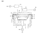
- FIG 1 is a schematic illustration of an embodiment of capacitive-coupled magnetic neutral loop plasma sputtering system according to the present invention, showing the configuration thereof
- FIG 2 is a schematic illustration of a magnetic potential contour map of the magnetic field produced in the vacuum chamber of the system of FIG 1 .
- FIG 3 is a graph illustrating the bias power dependency of the film forming rate of a system according to the present invention.
- FIG 4 is a graph illustrating the relationship between the target-substrate distance and the film thickness distribution observed after forming film for 1 minute in a system according to the present invention.
- FIG 5 is a graph illustration the dependency on the diameter of the magnetic neutral loop of the distribution of film deposition in a system according to the present invention.
- FIG 6 is a schematic illustration of another embodiment of capacitive-coupled magnetic neutral loop plasma sputtering system according to the present invention, showing the configuration thereof.
- FIG 7 is a schematic illustration of still another embodiment of capacitive-coupled magnetic neutral loop plasma sputtering system according to the present invention, showing the configuration thereof
- FIG 1 is a schematic illustration of an embodiment of capacitive-coupled magnetic neutral loop plasma sputtering system according to the present invention, showing the configuration thereof
- 1 denotes a vacuum chamber in which a target 2 and a substrate 3 are arranged oppositely to face each other and the substrate 3 is mounted on a substrate holder 4.
- the vacuum chamber 1 is connected to an appropriate exhaust pump (not shown) by way of an exhaust port 5.
- the intensities of the electric currents that are respectively made to flow through the three electromagnetic coils 6, 7 and 8 are so selected as to make the intensity of the magnetic field equal to 2 gausses within 1cm from the zero magnetic field region.
- the position and the size of the magnetic neutral loop 9 can be selected appropriately by changing the ratio of the electric currents that are respectively made to flow through the upper, intermediate and lower electromagnetic coils 6, 7 and 8.
- the magnetic neutral loop 9 is pushed down toward the electromagnetic coil 8 when the intensity of the electric current flowing through the upper electromagnetic coil 6 is made greater than the intensity of the electric current flowing through the lower electromagnetic coil 8, whereas the magnetic neutral loop 9 is pushed up toward the electromagnetic coil 6 when the intensity of the electric current flowing through the upper electromagnetic coil 6 is made smaller than the intensity of the electric current flowing through the lower electromagnetic coil 8.
- the diameter of the magnetic neutral loop 9 is reduced and, at the same time, the magnetic field gradient becomes milder in the zero magnetic field region as the electric current that flows through the intermediate electromagnetic coil 7 is increased.
- Deposition preventing members 10, 11 are arranged oppositely relative to each other with the region between the target 2 and the substrate 3 interposed between them in the vacuum chamber 1.
- a conductive ceiling board 13 is fitted to the top edge of the vacuum chamber 1 by way of an insulator 12 to airtightly seal and ensure vacuum in the vacuum chamber 1.
- the ceiling board 13 is connected to a high-frequency power source 15 by way of a matching box 14 so as to operate as a cathode electrode.
- the frequency of the high-frequency power source 15 is 20 to 100 MHz.
- Normal lines relative to the magnetic potential contour lines of the magnetic field produced by the electromagnetic coils 6, 7 and 8 in the vacuum chamber 1 as illustrated in FIG 2 show the directions of lines of magnetic force.
- a region of zero magnetic field is produced in the inside of the electromagnetic coil 7 as the magnetic field tends to negate itself
- Electrons generated in the vicinity of the zero magnetic field gather in the zero magnetic field due to the gradB drift. The extent of the gathering depends on the magnetic field gradient in the vicinity of the zero magnetic field. Equilibrium of electrons is established in the plasma in the course of generation, residence and extinction of electrons.
- high-density plasma can be produced by reducing the extinction of electrons.
- the magnetic field gradient takes the role of reducing the extinction of electrons. As the magnetic field gradient is raised, a large group of electrons tends to gather in the vicinity of the zero magnetic field to make it difficult to realize uniform sputtering. However, the non-uniformity of sputtering is negligible if compared with the magnetron discharge.
- CCP plasma can be sustained as secondary electrons are generated from the substrate 3 and the plasma sheath is heated at the sheath edge.
- the probability of emission of secondary electrons of metal is about 0.2, although it depends on the material of the target 2, it is safe to assume that CCP plasma can be sustained mainly by a heating the sheath.
- Heating the sheath means that the electric potential of the plasma in the vacuum chamber fluctuates as the target bias is made to fluctuate by the high-frequency bias and the group of electrons located at the edge of the sheath is accelerated in plasma by the fluctuations.
- the frequency of heating the sheath rises as the frequency (of the high-frequency bias?) rises to raise the plasma density This effect is referred to as f square law.
- a pressure level of lower than 1 Pa is required for film formation by sputtering.
- sputtering particles are required to fly from the target 2 to the substrate 3 without experiencing any collision. This is a requirement that needs to be indispensably met for forming fine film.
- the lower limit pressure for electric discharges for conventional CCP sputtering is about 2 Pa and the mean free path as converted to nitrogen molecules is about 3 mm Flying sputtering particles collide with each other repeatedly not less than ten times before they get to the substrate 3 and clustering of sputtering particles takes place as they fly to form large masses, which then fall onto the substrate 3.
- the film formed in this way is coarse and rough in quality
- FIG 3 is a graph illustrating the bias power dependency of the film forming rate of a system 1 according to the present invention, when the distance between the target 2 and the substrate 3 is about 80 mm.
- the pressure is 0.5 Pa in an Ar atmosphere.
- the graph also shows the power dependency of the film forming rate of conventional CCP sputtering, using 13.56 MHz.
- FIG 4 is a graph illustrating the relationship between the target-substrate distance and the film thickness distribution observed after forming film for 1 minute.
- the pressure is 0.5 Pa in an Ar atmosphere and electric power of 400W is applied to the target 2.
- the film forming rate rises but the uniformity of the formed film is degraded as the distance between the target 2 and the substrate 3 is reduced.
- FIG 5 is a graph illustrating the dependency on the diameter of the magnetic neutral loop of the distribution of film deposition in a system according to the present invention.
- the diameter of the magnetic neutral loop 9 can be changed by changing the electric current flowing through the intermediate coil 5 to consequently change the plasma distribution. While the distribution of erosion is sensitive to the diameter of the magnetic neutral loop 9, the distribution of film deposition is relatively insensitive to the diameter of the magnetic neutral loop 9 so that the sputtering process can be conducted mainly by taking the region of erosion into consideration.
- high-density plasma can be produced by increasing the quantity of electrons confined in the vicinity of the zero magnetic field to provide a sputtering system showing a high efficiency of utilization of target and adapted to a large sputtering area.
- FIG 6 is a schematic illustration of another embodiment of capacitive-coupled magnetic neutral loop plasma sputtering system according to the present invention, showing the configuration thereof
- the components that correspond to those of the system of the embodiment of FIG 1 are denoted respectively by the same reflectance symbols.
- a target 2 and a substrate 3 are arranged oppositely to face each other in a vacuum chamber 1 and the substrate 3 is mounted on a substrate holder 4.
- the vacuum chamber 1 is connected to an appropriate exhaust pump (not shown) by way of an exhaust port 5.
- the intensities of the electric currents that are respectively made to flow through the three electromagnetic coils 6, 7 and 8 are so selected as to make the intensity of the magnetic field equal to 2 gausses within 1cm from the zero magnetic field region.
- the position and the size of the magnetic neutral loop 9 can be selected appropriately by changing the ratio of the electric currents that are respectively made to flow through the upper, intermediate and lower electromagnetic coils 6, 7 and 8.
- the magnetic neutral loop 9 is pushed down toward the electromagnetic coil 8 when the intensity of the electric current flowing through the upper electromagnetic coil 6 is made greater than the intensity of the electric current flowing through the lower electromagnetic coil 8, whereas the magnetic neutral loop 9 is pushed up toward the electromagnetic coil 6 when the intensity of the electric current flowing through the upper electromagnetic coil 6 is made smaller than the intensity of the electric current flowing through the lower electromagnetic coil 8.
- the diameter of the magnetic neutral loop 9 is reduced and, at the same time, the magnetic field gradient becomes milder in the zero magnetic field region as the electric current that flowing through the intermediate electromagnetic coil 7 is increased.
- Deposition preventing members 10 and 11 are arranged oppositely relative to each other with the region between the target 2 and the substrate 3 interposed between them in the vacuum chamber 1.
- a conductive ceiling board 13 is fitted to the top edge of the vacuum chamber 1 by way of an insulator 12 to airtightly seal and ensure vacuum in the vacuum chamber 1.
- the ceiling board 13 is connected to a high-frequency power source 15 by way of a matching box 14 at one hand and to a direct current source 17 by way of a high frequency filter 16 at the other so that the DC voltage from the direct current source 17 is superposed on the high-frequency power from the high-frequency power source 15 before they are applied to the conductive ceiling board 15.
- the frequency of the high-frequency power source 15 is 20 to 100 MHz.
- a high-frequency bias power 18 is connected to the substrate holder 4 on which the substrate 3 is mounted in the embodiment of FIG 6 .
- the high-frequency bias power 18 applies a high-frequency bias of 40 to 100MHz to the substrate 3.
- FIG 7 is a schematic illustration of still another embodiment of capacitive-coupled magnetic neutral loop plasma sputtering system according to the present invention, showing the configuration thereof
- the components that correspond to those of the system of the embodiment of FIG. 1 are denoted respectively by the same reflectance symbols.
- a target 2 and a substrate 3 are arranged oppositely to face each other in a vacuum chamber 1 and the substrate 3 is mounted on a substrate holder 4.
- the vacuum chamber 1 is connected to an appropriate exhaust pump (not shown) by way of an exhaust port 5.
- the intensities of the electric currents that are respectively made to flow through the three electromagnetic coils 6, 7 and 8 are so selected as to make the intensity of the magnetic field equal to 2 gausses within 1cm from the zero magnetic field region.
- the position and the size of the magnetic neutral loop 9 can be selected appropriately by changing the ratio of the electric currents that are respectively made to flow through the upper, intermediate and lower electromagnetic coils 6, 7 and 8.
- the magnetic neutral loop 9 is pushed down toward the electromagnetic coil 8 when the intensity of the electric current flowing through the upper electromagnetic coil 6 is made greater than the intensity of the electric current flowing through the lower electromagnetic coil 8, whereas the magnetic neutral loop 9 is pushed up toward the electromagnetic coil 6 when the intensity of the electric current flowing through the upper electromagnetic coil 6 is made smaller than the intensity of the electric current flowing through the lower electromagnetic coil 8.
- the diameter of the magnetic neutral loop 9 is reduced and, at the same time, the magnetic field gradient becomes milder in the zero magnetic field region as the electric current that flows through the intermediate electromagnetic coil 7 is increased.
- Deposition preventing members 10, 11 are arranged oppositely relative to each other with the region between the target 2 and the substrate 3 interposed between them in the vacuum chamber 1 in the illustrated embodiment.
- a conductive ceiling board 13 is fitted to the top edge of the vacuum chamber 1 by way of an insulator 12 to airtightly seal and ensure vacuum in the vacuum chamber 1.
- the ceiling board 13 is connected to a high-frequency power source 15 by way of a matching box 14 at one hand and to a low-frequency power source 20 by way of another matching box 19 so that the low-frequency voltage from the low-frequency voltage source 20 is superposed on the high-frequency power from the high-frequency power source 15 before they are applied to the conductive ceiling board 15.
- the frequency of the high-frequency power source 15 is 20 to 100 MHz
- a frequency low-frequency power source 20 is 100 kHz to 4 MHz..
- a high-frequency bias power 18 is connected to the substrate holder 4 on which the substrate 3 is mounted in the embodiment of FIG 7 as in the case of the embodiment of FIG. 6 .
- the high-frequency bias power 18 applies a high-frequency bias power of 40 to 100 MHz to the substrate 3.
- each of the components and the conditions of operation thereof can be selected appropriately as described above for the embodiment of FIG. 1 .
- the operation, the function and the advantages of each of the systems of FIGS. 6 and 7 are substantially same as those described above for the embodiment of FIG. 1 by referring to FIGS. 3 through 5 .
Landscapes
- Chemical & Material Sciences (AREA)
- Engineering & Computer Science (AREA)
- Physics & Mathematics (AREA)
- Plasma & Fusion (AREA)
- Analytical Chemistry (AREA)
- Chemical Kinetics & Catalysis (AREA)
- Materials Engineering (AREA)
- Mechanical Engineering (AREA)
- Metallurgy (AREA)
- Organic Chemistry (AREA)
- Spectroscopy & Molecular Physics (AREA)
- Electromagnetism (AREA)
- Physical Vapour Deposition (AREA)
- Plasma Technology (AREA)
Abstract
Description
- This invention relates to a capacitive-coupled magnetic neutral loop (or neutral loop discharge-NLD) plasma sputtering system to be used for highly uniformly forming film on a large area substrate to manufacture electronic devices, semiconductor devices and functional thin films.
- DC bias sputtering is being popularly employed as sputtering technique for forming metal thin films.
High-frequency bias and pulse bias DC sputtering systems are being employed for forming insulating films. Such sputtering systems utilize magnetron discharges due to the ExB drift phenomenon that can be made to appear by the magnetic field produced by a permanent magnet and a bias electric field for the purpose of raising the film forming rate of the sputtering system, - On the other hand, an ICP (inductively coupled plasma) type low pressure high density neutral loop plasma source designed to form a neutral loop by arranging three cylindrical coils outside a vacuum chamber and generate plasma along the neutral loop has been proposed (see Patent Document 1).
- Patent Document 1: Jpn. Pat. Appln. Laid-Open Publication No.
07-090632 - The most significant problem of magnetron sputtering is the use efficiency of target. Since magnetron sputtering utilizes the sputter produced by local high density plasma in ExB drift regions, the region of erosion is localized and the efficiency of utilization of target is limited if the magnet is driven to rotate. Additionally, there is a problem of damaging devices due to charge up because the lines of magnetic force are distributed in such a way that they have an oblique component relative to the substrate.
- For these reasons, there has been a strong demand for uniform sputtering techniques using low pressure high density plasma, although no technique has been proposed to date to surpass magnetron sputtering. While the magnetron sputtering method is currently a state of the good film forming method, it is always accompanied by a problem that the use efficiency of target is lower than 50% and it is very difficult to arrange a magnetic field for uniform film formation.
- On the other hand, while an ICP type plasma source can produce uniform and high density plasma, high-frequency power needs to be introduced into the vacuum barriers arranged near the antennas thereof so that the vacuum barriers arranged near the antennas need to be formed by using a dielectric. Therefore, such a plasma source cannot be applied to metal film formation. In other words, when an ICP type plasma source is employed for forming film by sputtering, metal film is formed on the inner surfaces of the dielectric barriers to shield the antenna electric fields for generating plasma so that the generated plasma cannot be sustained.
- Additionally, a conventional plasma source that does not utilize any magnetic field requires a high discharge voltage. Then, sputtering particles collide with each other in a gas phase as large clusters, which then adhere to the surface to produce a coarse film,
- In view of the above-identified technical problems of the prior art, it is therefore the object of the present invention to provide a capacitive-coupled magnetic neutral loop discharge plasma sputtering system having a structure that can uniformly sputter a target to dramatically raise the use efficiency of target and produce lines of magnetic force that are distributed uniformly so as not to produce any charge up.
- According to the present invention, the above object is achieved by providing a capacitive-coupled magnetic neutral loop (or neutral loop discharge-NLD) plasma sputtering system including: a vacuum chamber; a target placed in the vacuum chamber; a magnetic field generation means for forming a magnetic neutral loop of zero magnetic field in the vacuum chamber; and an electric field generation means for generating plasma along the magnetic neutral loop by applying a high-frequency bias to the target; the magnetic field gradient being set at 2 gauss/cm or above in the vicinity of the zero magnetic field of the magnetic neutral loop for sputtering the target by plasma and forming film on a substrate placed oppositely relative to the target.
- In a capacitive-coupled magnetic neutral loop plasma sputtering system according to the present invention, the frequency of electric power applied to the electric field generation means may be not less than 13.56 MHz, preferably not less than 20 MHz.
- Further, the magnetic field generation means may have three cylindrical coils so as to form a magnetic neutral loop at an arbitrarily selected position in the vacuum chamber by means of an arbitrarily selected magnetic field gradient.
- The electric field generation means may have a conductive ceiling board fitted to the top edge of the vacuum chamber by way of an insulator to airtightly seal and ensure vacuum in the vacuum chamber and a high-frequency power source connected to said ceiling board to apply high frequency power to said ceiling board.
- In a capacitive-coupled magnetic neutral loop plasma sputtering system according to the present invention, the target may be a metal target.
- A capacitive-coupled magnetic neutral loop plasma sputtering system according to the present invention may further comprise an RF power source connected to a substrate holder for placing the substrate in position and applying a bias to the substrate.
- A capacitive-coupled magnetic neutral loop plasma sputtering system according to the present invention may further comprise a DC power source connected to the target placed in position in the system to superpose a DC voltage.
- In a capacitive-coupled magnetic neutral loop plasma sputtering system according to the present invention, the DC power source may be connected to the ceiling board by way of a high-frequency filter.
- A capacitive-coupled magnetic neutral loop plasma sputtering system according to the present invention may further comprise a low-frequency (bias?) generation means connected to the target placed in position in the system to superpose a low-frequency bias onto the target.
- In a capacitive-coupled magnetic neutral loop plasma sputtering system, the low-frequency generation means may have a low-frequency power source and a matching unit for connecting the low-frequency power source to the ceiling board.
- A capacitive-coupled magnetic neutral loop plasma sputtering system according to the present invention may further comprise an anti-deposition member arranged in the vacuum chamber so as to surround the region between the target and the substrate.
- A capacitive-coupled magnetic neutral loop plasma sputtering system according to the present invention captures electrons in the vicinity of the zero magnetic field by means of a magnetic field gradient and efficiently accelerates electrons in a high-frequency electric field to generate high density plasma when the magnetic field gradient is set to 2 gauss/cm or above in the vicinity of the zero magnetic field of the magnetic neutral loop. As a result, the present invention provides an advantage that not only the target is sputtered uniformly to dramatically increase the use efficiency of the target but also lines of magnetic force are perpendicular relative to the substrate and distributed uniformly in the vicinity of the substrate to prevent any charge up from taking place.
- When the frequency of electric power applied to the electric field generation means is increased above 13.56 MHz in order to raise the plasma density, electrons that are captured in the vicinity of the zero magnetic field due to the magnetic field gradient are increased to a large extent because of the raised plasma density so that the high-frequency electric field can be absorbed efficiently Then, as a result, plasma can be obtained with a density level of 1011 cm-3. For comparison, the plasma density that can be produced by magnetron is at the level of 1011 cm-3 in the ExB drift area and at the level of 110 cm-3 in areas (of a vertical magnetic field) remote from the ExB drift area to show remarkable density variances. However, the above-described arrangement according to the present invention can produce high density and uniform plasma. Therefore, while the use efficiency of target is less than 50% and maximally about 45% with magnetron sputtering, it can be as high as 50 to 70% according to the present invention.
- Additionally, as a result of raising the efficiency of capturing electrons by means of a magnetic field by increasing the magnetic field gradient in the vicinity of the zero magnetic field and setting the frequency of the bias high-frequency power source at 20 MHz or above, a high efficiency is realized for absorption of high-frequency power by electrons to achieve a high density for CCP type NLD plasma that has hitherto been difficult to achieve so that the present invention find applications for metal sputtering systems.
- Still additionally, as a result of using a cathode coupled plasma (CCP) source according to the present invention, it is no longer necessary to install an electric field generation means in a vacuum chamber unlike ICP plasma generators and not to form the wall of the vacuum chamber by using a dielectric. Thus, plasma can be generated without obstructing introduction of an electric field when forming metal film
- While the discharge pressure is 2Pa or above in ordinary cathode coupled plasma sources, electric discharges can be produced under pressure lower than 2Pa, or even lower than 1 Pa, by using NLD. As a result, the free path of sputtering particles is increased to make it possible to from fine film.
- Furthermore, when an arrangement of adding a high-frequency power source to the target and connecting a DC power source or a low-frequency power source to the target for voltage superposition is adopted, the sputtering process can be controlled with ease because the bias applied to the target and the introduction of an electric field (high-frequency) can be controlled separately
- Finally, as a bias is applied to the substrate, plasma is generated around the substrate to raise the ionization ratio. The deposited film is hit by ions to make the film finer or raise the coverage.
-
FIG 1 is a schematic illustration of an embodiment of capacitive-coupled magnetic neutral loop plasma sputtering system according to the present invention, showing the configuration thereof -
FIG 2 is a schematic illustration of a magnetic potential contour map of the magnetic field produced in the vacuum chamber of the system ofFIG 1 . -
FIG 3 is a graph illustrating the bias power dependency of the film forming rate of a system according to the present invention. -
FIG 4 is a graph illustrating the relationship between the target-substrate distance and the film thickness distribution observed after forming film for 1 minute in a system according to the present invention. -
FIG 5 is a graph illustration the dependency on the diameter of the magnetic neutral loop of the distribution of film deposition in a system according to the present invention. -
FIG 6 is a schematic illustration of another embodiment of capacitive-coupled magnetic neutral loop plasma sputtering system according to the present invention, showing the configuration thereof. -
FIG 7 is a schematic illustration of still another embodiment of capacitive-coupled magnetic neutral loop plasma sputtering system according to the present invention, showing the configuration thereof - Now, the present invention will be described by referring to the accompanying drawings that illustrate an embodiment of the present invention.
-
FIG 1 is a schematic illustration of an embodiment of capacitive-coupled magnetic neutral loop plasma sputtering system according to the present invention, showing the configuration thereof In the illustrated system, 1 denotes a vacuum chamber in which atarget 2 and asubstrate 3 are arranged oppositely to face each other and thesubstrate 3 is mounted on asubstrate holder 4. Thevacuum chamber 1 is connected to an appropriate exhaust pump (not shown) by way of anexhaust port 5. - As shown, three
electromagnetic coils vacuum chamber 1 and constant electric currents are respectively made to flow through the upper and lowerelectromagnetic coils electromagnetic coil 7 in the opposite direction. As a result, a continuous zero magnetic field region is formed in thevacuum chamber 1 at the level of the intermediateelectromagnetic coil 7 to form a magneticneutral loop 9 as seen from the magnetic potential contour map inFIG. 2 . According to the present invention, the intensities of the electric currents that are respectively made to flow through the threeelectromagnetic coils neutral loop 9 can be selected appropriately by changing the ratio of the electric currents that are respectively made to flow through the upper, intermediate and lowerelectromagnetic coils neutral loop 9 is pushed down toward theelectromagnetic coil 8 when the intensity of the electric current flowing through the upperelectromagnetic coil 6 is made greater than the intensity of the electric current flowing through the lowerelectromagnetic coil 8, whereas the magneticneutral loop 9 is pushed up toward theelectromagnetic coil 6 when the intensity of the electric current flowing through the upperelectromagnetic coil 6 is made smaller than the intensity of the electric current flowing through the lowerelectromagnetic coil 8. The diameter of the magneticneutral loop 9 is reduced and, at the same time, the magnetic field gradient becomes milder in the zero magnetic field region as the electric current that flows through the intermediateelectromagnetic coil 7 is increased. -
Deposition preventing members target 2 and thesubstrate 3 interposed between them in thevacuum chamber 1. On the other hand, aconductive ceiling board 13 is fitted to the top edge of thevacuum chamber 1 by way of aninsulator 12 to airtightly seal and ensure vacuum in thevacuum chamber 1. Theceiling board 13 is connected to a high-frequency power source 15 by way of amatching box 14 so as to operate as a cathode electrode. The frequency of the high-frequency power source 15 is 20 to 100 MHz. - Normal lines relative to the magnetic potential contour lines of the magnetic field produced by the
electromagnetic coils vacuum chamber 1 as illustrated inFIG 2 show the directions of lines of magnetic force. A region of zero magnetic field is produced in the inside of theelectromagnetic coil 7 as the magnetic field tends to negate itself Electrons generated in the vicinity of the zero magnetic field gather in the zero magnetic field due to the gradB drift. The extent of the gathering depends on the magnetic field gradient in the vicinity of the zero magnetic field. Equilibrium of electrons is established in the plasma in the course of generation, residence and extinction of electrons. - To produce high-density plasma under low pressure, it is necessary to raise the efficiency of generation and minimize the extinction of electrons. Given the efficiency of generation, high-density plasma can be produced by reducing the extinction of electrons. The magnetic field gradient takes the role of reducing the extinction of electrons. As the magnetic field gradient is raised, a large group of electrons tends to gather in the vicinity of the zero magnetic field to make it difficult to realize uniform sputtering. However, the non-uniformity of sputtering is negligible if compared with the magnetron discharge.
- Another way for forming high-density plasma is to raise the efficiency of generation of electrons. CCP plasma can be sustained as secondary electrons are generated from the
substrate 3 and the plasma sheath is heated at the sheath edge. In view of that the probability of emission of secondary electrons of metal is about 0.2, although it depends on the material of thetarget 2, it is safe to assume that CCP plasma can be sustained mainly by a heating the sheath. Heating the sheath means that the electric potential of the plasma in the vacuum chamber fluctuates as the target bias is made to fluctuate by the high-frequency bias and the group of electrons located at the edge of the sheath is accelerated in plasma by the fluctuations. The frequency of heating the sheath rises as the frequency (of the high-frequency bias?) rises to raise the plasma density This effect is referred to as f square law. - The use of a magnetic field provides another additional advantage that the discharge voltage can be reduced by the electron trapping effect. A pressure level of lower than 1 Pa is required for film formation by sputtering. In other words, sputtering particles are required to fly from the
target 2 to thesubstrate 3 without experiencing any collision. This is a requirement that needs to be indispensably met for forming fine film. The lower limit pressure for electric discharges for conventional CCP sputtering is about 2 Pa and the mean free path as converted to nitrogen molecules is about 3 mm Flying sputtering particles collide with each other repeatedly not less than ten times before they get to thesubstrate 3 and clustering of sputtering particles takes place as they fly to form large masses, which then fall onto thesubstrate 3. The film formed in this way is coarse and rough in quality -
FIG 3 is a graph illustrating the bias power dependency of the film forming rate of asystem 1 according to the present invention, when the distance between thetarget 2 and thesubstrate 3 is about 80 mm. The pressure is 0.5 Pa in an Ar atmosphere. For the purpose of comparison, the graph also shows the power dependency of the film forming rate of conventional CCP sputtering, using 13.56 MHz. -
FIG 4 is a graph illustrating the relationship between the target-substrate distance and the film thickness distribution observed after forming film for 1 minute. The pressure is 0.5 Pa in an Ar atmosphere and electric power of 400W is applied to thetarget 2. As seen fromFIG 4 , while the film forming rate rises but the uniformity of the formed film is degraded as the distance between thetarget 2 and thesubstrate 3 is reduced. -
FIG 5 is a graph illustrating the dependency on the diameter of the magnetic neutral loop of the distribution of film deposition in a system according to the present invention. The diameter of the magneticneutral loop 9 can be changed by changing the electric current flowing through theintermediate coil 5 to consequently change the plasma distribution. While the distribution of erosion is sensitive to the diameter of the magneticneutral loop 9, the distribution of film deposition is relatively insensitive to the diameter of the magneticneutral loop 9 so that the sputtering process can be conducted mainly by taking the region of erosion into consideration. - In view of the above description, high-density plasma can be produced by increasing the quantity of electrons confined in the vicinity of the zero magnetic field to provide a sputtering system showing a high efficiency of utilization of target and adapted to a large sputtering area.
-
FIG 6 is a schematic illustration of another embodiment of capacitive-coupled magnetic neutral loop plasma sputtering system according to the present invention, showing the configuration thereof InFIG 6 , the components that correspond to those of the system of the embodiment ofFIG 1 are denoted respectively by the same reflectance symbols. Referring toFIG 6 , atarget 2 and asubstrate 3 are arranged oppositely to face each other in avacuum chamber 1 and thesubstrate 3 is mounted on asubstrate holder 4. Thevacuum chamber 1 is connected to an appropriate exhaust pump (not shown) by way of anexhaust port 5. - As shown, three
electromagnetic coils vacuum chamber 1 and constant electric currents are respectively made to flow through the upper and lowerelectromagnetic coils electromagnetic coil 7 in the opposite direction. As a result, a continuous zero magnetic field region is formed in thevacuum chamber 1 at the level of theintermediate coil 7 to form a magneticneutral loop 9 as seen from the magnetic potential contour map inFIG 2 . According to the present invention, the intensities of the electric currents that are respectively made to flow through the threeelectromagnetic coils neutral loop 9 can be selected appropriately by changing the ratio of the electric currents that are respectively made to flow through the upper, intermediate and lowerelectromagnetic coils neutral loop 9 is pushed down toward theelectromagnetic coil 8 when the intensity of the electric current flowing through the upperelectromagnetic coil 6 is made greater than the intensity of the electric current flowing through the lowerelectromagnetic coil 8, whereas the magneticneutral loop 9 is pushed up toward theelectromagnetic coil 6 when the intensity of the electric current flowing through the upperelectromagnetic coil 6 is made smaller than the intensity of the electric current flowing through the lowerelectromagnetic coil 8. The diameter of the magneticneutral loop 9 is reduced and, at the same time, the magnetic field gradient becomes milder in the zero magnetic field region as the electric current that flowing through the intermediateelectromagnetic coil 7 is increased. -
Deposition preventing members target 2 and thesubstrate 3 interposed between them in thevacuum chamber 1. On the other hand, aconductive ceiling board 13 is fitted to the top edge of thevacuum chamber 1 by way of aninsulator 12 to airtightly seal and ensure vacuum in thevacuum chamber 1. Theceiling board 13 is connected to a high-frequency power source 15 by way of amatching box 14 at one hand and to a directcurrent source 17 by way of ahigh frequency filter 16 at the other so that the DC voltage from the directcurrent source 17 is superposed on the high-frequency power from the high-frequency power source 15 before they are applied to theconductive ceiling board 15. The frequency of the high-frequency power source 15 is 20 to 100 MHz. - Additionally, a high-
frequency bias power 18 is connected to thesubstrate holder 4 on which thesubstrate 3 is mounted in the embodiment ofFIG 6 . The high-frequency bias power 18 applies a high-frequency bias of 40 to 100MHz to thesubstrate 3. -
FIG 7 is a schematic illustration of still another embodiment of capacitive-coupled magnetic neutral loop plasma sputtering system according to the present invention, showing the configuration thereof In the system shown inFIG 7 , the components that correspond to those of the system of the embodiment ofFIG. 1 are denoted respectively by the same reflectance symbols. Referring toFIG 7 , atarget 2 and asubstrate 3 are arranged oppositely to face each other in avacuum chamber 1 and thesubstrate 3 is mounted on asubstrate holder 4. Thevacuum chamber 1 is connected to an appropriate exhaust pump (not shown) by way of anexhaust port 5. - As shown, three
electromagnetic coils vacuum chamber 1 and constant electric currents are respectively made to flow through the upper and lowerelectromagnetic coils electromagnetic coil 7 in the opposite direction. As a result, a continuous zero magnetic field region is formed in thevacuum chamber 1 at the level of theintermediate coil 7 to form a magneticneutral loop 9 as seen from the magnetic potential contour map inFIG 2 . According to the present invention, the intensities of the electric currents that are respectively made to flow through the threeelectromagnetic coils neutral loop 9 can be selected appropriately by changing the ratio of the electric currents that are respectively made to flow through the upper, intermediate and lowerelectromagnetic coils neutral loop 9 is pushed down toward theelectromagnetic coil 8 when the intensity of the electric current flowing through the upperelectromagnetic coil 6 is made greater than the intensity of the electric current flowing through the lowerelectromagnetic coil 8, whereas the magneticneutral loop 9 is pushed up toward theelectromagnetic coil 6 when the intensity of the electric current flowing through the upperelectromagnetic coil 6 is made smaller than the intensity of the electric current flowing through the lowerelectromagnetic coil 8. The diameter of the magneticneutral loop 9 is reduced and, at the same time, the magnetic field gradient becomes milder in the zero magnetic field region as the electric current that flows through the intermediateelectromagnetic coil 7 is increased. -
Deposition preventing members target 2 and thesubstrate 3 interposed between them in thevacuum chamber 1 in the illustrated embodiment. On the other hand, aconductive ceiling board 13 is fitted to the top edge of thevacuum chamber 1 by way of aninsulator 12 to airtightly seal and ensure vacuum in thevacuum chamber 1. Theceiling board 13 is connected to a high-frequency power source 15 by way of amatching box 14 at one hand and to a low-frequency power source 20 by way of anothermatching box 19 so that the low-frequency voltage from the low-frequency voltage source 20 is superposed on the high-frequency power from the high-frequency power source 15 before they are applied to theconductive ceiling board 15. The frequency of the high-frequency power source 15 is 20 to 100 MHz, and a frequency low-frequency power source 20 is 100 kHz to 4 MHz.. - Additionally, a high-
frequency bias power 18 is connected to thesubstrate holder 4 on which thesubstrate 3 is mounted in the embodiment ofFIG 7 as in the case of the embodiment ofFIG. 6 . The high-frequency bias power 18 applies a high-frequency bias power of 40 to 100 MHz to thesubstrate 3. - In the systems of
FIGS. 6 and7 , the operation of each of the components and the conditions of operation thereof can be selected appropriately as described above for the embodiment ofFIG. 1 . The operation, the function and the advantages of each of the systems ofFIGS. 6 and7 are substantially same as those described above for the embodiment ofFIG. 1 by referring toFIGS. 3 through 5 . -
- 1:
- vacuum chamber
- 2:
- target
- 3:
- substrate
- 4:
- substrate holder
- 5:
- exhaust port
- 6:
- electromagnetic coil
- 7:
- electromagnetic coil
- 8:
- electromagnetic coil
- 9:
- magnetic neutral loop
- 10:
- deposition preventing member
- 11:
- deposition preventing member
- 12:
- insulator
- 13;
- conductive ceiling board
- 14:
- matching box
- 15:
- high-frequency power source
- 16:
- high-frequency filter
- 17:
- direct current source
- 18:
- high-frequency bias power
- 19:
- matching box
- 20:
- low-frequency power source
Claims (13)
- A capacitive-coupled magnetic neutral loop (or neutral loop discharge-NLD) plasma sputtering system comprising:a vacuum chamber (1);a target (2) placed oppositely relative to a substrate (3) in the vacuum chamber (1);a magnetic field generation means (6, 7, 8) for forming a magnetic neutral loop (9) of zero magnetic field in the vacuum chamber (1); andan electric field generation means (13, 15) for generating plasma along the magnetic neutral loop (9) by applying a high-frequency bias to the target (2);the magnetic field gradient being set at 2 gauss/cm or above in the vicinity of the zero magnetic field of said magnetic neutral loop (9) for sputtering said target by plasma and forming film on a substrate (3) placed oppositely relative to said target (2).
- A system according to claim 1, wherein
the frequency of electric power applied to said electric field generation means (13, 15) is not less than 13.56 MHz. - A system according to claim 1, wherein
the frequency of electric power applied to said electric field generation means (13, 15) is not less than 20 MHz. - A system according to claim 1, wherein
said magnetic field generation means has three cylindrical coils (6, 7, 8) so as to form a magnetic neutral loop (9) at an arbitrarily selected position by means of an arbitrarily selected magnetic field gradient. - A system according to claim 1, wherein
said electric field generation means has a conductive ceiling board (13) fitted to the top edge of the vacuum chamber (1) by way of an insulator (12) to airtightly seal and ensure vacuum in the vacuum chamber (1) and a high-frequency power source (15) connected to said ceiling board (13) to apply high-frequency power to said ceiling board (13). - A system according to claim 5, wherein
said target (2) is fitted to the inner surface of said conductive ceiling board (13). - A system according to claim 1, wherein
said target (2) is a metal target. - A system according to claim 1, wherein it further comprises:an RF power source (18) connected to a substrate holder (4) for placing said substrate (3) in position and applying a bias to said substrate (3).
- A system according to claim 1, wherein it further comprises:a DC power source (17) connected to said target (2) placed in position in said system to superpose a DC voltage.
- A system according to claim 5, wherein
said DC power source (17) is connected to said ceiling board (13) by way of a high-frequency filter (16). - A system according to claim 1, wherein it further comprises:a low-frequency generation means (19, 20) connected to said target (2) placed in position in said system to superpose a low-frequency bias onto said target (2).
- A system according to claim 5, wherein
said low-frequency generation means may has a low-frequency power source (20) and a matching unit (19) for connecting said low-frequency power source (20) to said ceiling board (13). - A system according to claim 1, wherein it further comprises:an anti-deposition member (10, 11) arranged in said vacuum chamber (1) so as to surround the region between said target (2) and said substrate (3).
Applications Claiming Priority (2)
| Application Number | Priority Date | Filing Date | Title |
|---|---|---|---|
| JP2006194105 | 2006-07-14 | ||
| PCT/JP2007/064016 WO2008007784A1 (en) | 2006-07-14 | 2007-07-13 | Capacitive-coupled magnetic neutral line plasma sputtering system |
Publications (3)
| Publication Number | Publication Date |
|---|---|
| EP2045353A1 true EP2045353A1 (en) | 2009-04-08 |
| EP2045353A4 EP2045353A4 (en) | 2010-06-30 |
| EP2045353B1 EP2045353B1 (en) | 2016-12-14 |
Family
ID=38923339
Family Applications (1)
| Application Number | Title | Priority Date | Filing Date |
|---|---|---|---|
| EP07790796.2A Ceased EP2045353B1 (en) | 2006-07-14 | 2007-07-13 | Capacitive-coupled magnetic neutral loop plasma sputtering system |
Country Status (6)
| Country | Link |
|---|---|
| US (1) | US20090314636A1 (en) |
| EP (1) | EP2045353B1 (en) |
| JP (1) | JP4945566B2 (en) |
| KR (1) | KR101141391B1 (en) |
| TW (1) | TW200821408A (en) |
| WO (1) | WO2008007784A1 (en) |
Cited By (1)
| Publication number | Priority date | Publication date | Assignee | Title |
|---|---|---|---|---|
| CN102812153A (en) * | 2010-03-09 | 2012-12-05 | Emd株式会社 | Sputtering device |
Families Citing this family (9)
| Publication number | Priority date | Publication date | Assignee | Title |
|---|---|---|---|---|
| JP5373903B2 (en) * | 2009-07-17 | 2013-12-18 | 株式会社アルバック | Deposition equipment |
| KR101151225B1 (en) * | 2010-04-23 | 2012-06-14 | 한국과학기술원 | Capactively coupled plasma generation apparatus and capactively coupled plasma generation method |
| WO2013036953A2 (en) * | 2011-09-09 | 2013-03-14 | Applied Materials, Inc. | Multiple frequency sputtering for enhancement in deposition rate and growth kinetics dielectric materials |
| US9499901B2 (en) * | 2012-01-27 | 2016-11-22 | Applied Materials, Inc. | High density TiN RF/DC PVD deposition with stress tuning |
| US11049725B1 (en) * | 2014-05-29 | 2021-06-29 | Corporation For National Research Initiatives | Method for etching deep, high-aspect ratio features into silicon carbide and gallium nitride |
| KR101985830B1 (en) * | 2017-05-23 | 2019-06-05 | (주)울텍 | physical vapor deposition apparatus |
| CN113774342A (en) * | 2020-06-09 | 2021-12-10 | 江苏菲沃泰纳米科技股份有限公司 | Sputtering coating equipment, electrode device thereof and coating method |
| CN114836735B (en) * | 2021-02-01 | 2024-01-19 | 江苏菲沃泰纳米科技股份有限公司 | Plasma coating device and method based on ICP |
| US11898236B2 (en) * | 2021-10-20 | 2024-02-13 | Applied Materials, Inc. | Methods and apparatus for processing a substrate |
Family Cites Families (15)
| Publication number | Priority date | Publication date | Assignee | Title |
|---|---|---|---|---|
| JPH06104898B2 (en) * | 1988-01-13 | 1994-12-21 | 忠弘 大見 | Decompression surface treatment equipment |
| JPH07263190A (en) * | 1994-03-24 | 1995-10-13 | Ulvac Japan Ltd | Discharge plasma processing device |
| JP2705897B2 (en) | 1993-07-26 | 1998-01-28 | 日本真空技術株式会社 | Discharge plasma processing equipment |
| US6475333B1 (en) * | 1993-07-26 | 2002-11-05 | Nihon Shinku Gijutsu Kabushiki Kaisha | Discharge plasma processing device |
| JPH07263189A (en) * | 1994-03-24 | 1995-10-13 | Ulvac Japan Ltd | Discharge plasma processing device |
| JP3177573B2 (en) * | 1995-02-20 | 2001-06-18 | 日本真空技術株式会社 | Magnetic neutral line discharge plasma processing equipment |
| JP3542475B2 (en) * | 1997-11-28 | 2004-07-14 | キヤノン株式会社 | Manufacturing method of membrane |
| US5976327A (en) * | 1997-12-12 | 1999-11-02 | Applied Materials, Inc. | Step coverage and overhang improvement by pedestal bias voltage modulation |
| US6103074A (en) * | 1998-02-14 | 2000-08-15 | Phygen, Inc. | Cathode arc vapor deposition method and apparatus |
| JP2003342713A (en) * | 2002-05-24 | 2003-12-03 | Toshiba Corp | Thin film deposition apparatus |
| JP2004022212A (en) * | 2002-06-12 | 2004-01-22 | Ulvac Japan Ltd | Magnetic neutral line electrical discharge plasma treatment device |
| JP2004022211A (en) * | 2002-06-12 | 2004-01-22 | Ulvac Japan Ltd | Discharge plasma processing equipment |
| DE10326135B4 (en) * | 2002-06-12 | 2014-12-24 | Ulvac, Inc. | A discharge plasma processing system |
| JP2005149956A (en) * | 2003-11-17 | 2005-06-09 | Ulvac Japan Ltd | Method and apparatus for performing plasma processing with high uniformity over large area |
| JP2005268235A (en) * | 2005-06-13 | 2005-09-29 | Ulvac Japan Ltd | Ion beam irradiation device and ion bean irradiation method |
-
2007
- 2007-07-13 US US12/373,580 patent/US20090314636A1/en not_active Abandoned
- 2007-07-13 WO PCT/JP2007/064016 patent/WO2008007784A1/en not_active Ceased
- 2007-07-13 EP EP07790796.2A patent/EP2045353B1/en not_active Ceased
- 2007-07-13 KR KR1020087032234A patent/KR101141391B1/en not_active Expired - Fee Related
- 2007-07-13 TW TW096125740A patent/TW200821408A/en unknown
- 2007-07-13 JP JP2008524865A patent/JP4945566B2/en active Active
Cited By (2)
| Publication number | Priority date | Publication date | Assignee | Title |
|---|---|---|---|---|
| CN102812153A (en) * | 2010-03-09 | 2012-12-05 | Emd株式会社 | Sputtering device |
| EP2546385A4 (en) * | 2010-03-09 | 2013-08-07 | Emd Corp | Sputtering device |
Also Published As
| Publication number | Publication date |
|---|---|
| JPWO2008007784A1 (en) | 2009-12-10 |
| JP4945566B2 (en) | 2012-06-06 |
| TW200821408A (en) | 2008-05-16 |
| KR101141391B1 (en) | 2012-05-03 |
| US20090314636A1 (en) | 2009-12-24 |
| EP2045353A4 (en) | 2010-06-30 |
| KR20090016610A (en) | 2009-02-16 |
| EP2045353B1 (en) | 2016-12-14 |
| WO2008007784A1 (en) | 2008-01-17 |
Similar Documents
| Publication | Publication Date | Title |
|---|---|---|
| EP2045353B1 (en) | Capacitive-coupled magnetic neutral loop plasma sputtering system | |
| US10815570B2 (en) | Linearized energetic radio-frequency plasma ion source | |
| KR100301749B1 (en) | Sputtering device and sputtering method | |
| KR100322330B1 (en) | Method and apparatus for ionized sputtering of materials | |
| EP1489643B1 (en) | Method and apparatus for ionized physical vapor deposition | |
| US6254737B1 (en) | Active shield for generating a plasma for sputtering | |
| US5961793A (en) | Method of reducing generation of particulate matter in a sputtering chamber | |
| US6514390B1 (en) | Method to eliminate coil sputtering in an ICP source | |
| US6368469B1 (en) | Coils for generating a plasma and for sputtering | |
| US6599399B2 (en) | Sputtering method to generate ionized metal plasma using electron beams and magnetic field | |
| US6660134B1 (en) | Feedthrough overlap coil | |
| CN1260842A (en) | Method and apparatus for low pressure sputtering | |
| JPH07188917A (en) | Collimation device | |
| JP2001257199A (en) | Plasma processing method and device thereof | |
| US8911602B2 (en) | Dual hexagonal shaped plasma source | |
| US6506287B1 (en) | Overlap design of one-turn coil | |
| EP0836219A2 (en) | Active shield for generating a plasma for sputtering | |
| EP2546385A1 (en) | Sputtering device | |
| US5397448A (en) | Device for generating a plasma by means of cathode sputtering and microwave-irradiation | |
| US6235169B1 (en) | Modulated power for ionized metal plasma deposition | |
| WO2000003055A1 (en) | Shield for ionized physical vapor deposition apparatus | |
| JP4614220B2 (en) | Sputtering apparatus and sputtering method | |
| WO2009048294A2 (en) | Magnetized inductively coupled plasma processing apparatus and generating method | |
| TW202603819A (en) | Shielding for immersed plasma source | |
| HK40036021A (en) | Linearized energetic radio-frequency plasma ion source |
Legal Events
| Date | Code | Title | Description |
|---|---|---|---|
| PUAI | Public reference made under article 153(3) epc to a published international application that has entered the european phase |
Free format text: ORIGINAL CODE: 0009012 |
|
| 17P | Request for examination filed |
Effective date: 20090109 |
|
| AK | Designated contracting states |
Kind code of ref document: A1 Designated state(s): AT BE BG CH CY CZ DE DK EE ES FI FR GB GR HU IE IS IT LI LT LU LV MC MT NL PL PT RO SE SI SK TR |
|
| AX | Request for extension of the european patent |
Extension state: AL BA HR MK RS |
|
| RBV | Designated contracting states (corrected) |
Designated state(s): DE |
|
| A4 | Supplementary search report drawn up and despatched |
Effective date: 20100531 |
|
| RIC1 | Information provided on ipc code assigned before grant |
Ipc: H01J 37/34 20060101ALI20100525BHEP Ipc: H05H 1/46 20060101ALI20100525BHEP Ipc: H01J 37/32 20060101ALN20100525BHEP Ipc: C23C 14/35 20060101AFI20080313BHEP |
|
| 17Q | First examination report despatched |
Effective date: 20111102 |
|
| DAX | Request for extension of the european patent (deleted) | ||
| GRAP | Despatch of communication of intention to grant a patent |
Free format text: ORIGINAL CODE: EPIDOSNIGR1 |
|
| RIC1 | Information provided on ipc code assigned before grant |
Ipc: H01J 37/32 20060101ALN20160601BHEP Ipc: H01J 37/34 20060101ALI20160601BHEP Ipc: C23C 14/35 20060101AFI20160601BHEP Ipc: H05H 1/46 20060101ALI20160601BHEP |
|
| INTG | Intention to grant announced |
Effective date: 20160627 |
|
| GRAS | Grant fee paid |
Free format text: ORIGINAL CODE: EPIDOSNIGR3 |
|
| STAA | Information on the status of an ep patent application or granted ep patent |
Free format text: STATUS: GRANT OF PATENT IS INTENDED |
|
| GRAA | (expected) grant |
Free format text: ORIGINAL CODE: 0009210 |
|
| STAA | Information on the status of an ep patent application or granted ep patent |
Free format text: STATUS: THE PATENT HAS BEEN GRANTED |
|
| AK | Designated contracting states |
Kind code of ref document: B1 Designated state(s): DE |
|
| REG | Reference to a national code |
Ref country code: DE Ref legal event code: R096 Ref document number: 602007049152 Country of ref document: DE |
|
| REG | Reference to a national code |
Ref country code: DE Ref legal event code: R097 Ref document number: 602007049152 Country of ref document: DE |
|
| PLBE | No opposition filed within time limit |
Free format text: ORIGINAL CODE: 0009261 |
|
| STAA | Information on the status of an ep patent application or granted ep patent |
Free format text: STATUS: NO OPPOSITION FILED WITHIN TIME LIMIT |
|
| 26N | No opposition filed |
Effective date: 20170915 |
|
| PGFP | Annual fee paid to national office [announced via postgrant information from national office to epo] |
Ref country code: DE Payment date: 20230719 Year of fee payment: 17 |
|
| REG | Reference to a national code |
Ref country code: DE Ref legal event code: R119 Ref document number: 602007049152 Country of ref document: DE |
|
| PG25 | Lapsed in a contracting state [announced via postgrant information from national office to epo] |
Ref country code: DE Free format text: LAPSE BECAUSE OF NON-PAYMENT OF DUE FEES Effective date: 20250201 |