EP2043239A1 - Method in connection with mains side converter - Google Patents
Method in connection with mains side converter Download PDFInfo
- Publication number
- EP2043239A1 EP2043239A1 EP07117326A EP07117326A EP2043239A1 EP 2043239 A1 EP2043239 A1 EP 2043239A1 EP 07117326 A EP07117326 A EP 07117326A EP 07117326 A EP07117326 A EP 07117326A EP 2043239 A1 EP2043239 A1 EP 2043239A1
- Authority
- EP
- European Patent Office
- Prior art keywords
- voltage
- phase
- determining
- voltage limit
- time instant
- Prior art date
- Legal status (The legal status is an assumption and is not a legal conclusion. Google has not performed a legal analysis and makes no representation as to the accuracy of the status listed.)
- Granted
Links
- 238000000034 method Methods 0.000 title claims abstract description 41
- 238000000819 phase cycle Methods 0.000 claims abstract description 18
- 239000013598 vector Substances 0.000 claims description 26
- 238000005259 measurement Methods 0.000 description 11
- 230000001360 synchronised effect Effects 0.000 description 6
- 239000004065 semiconductor Substances 0.000 description 5
- 239000003990 capacitor Substances 0.000 description 4
- 230000000630 rising effect Effects 0.000 description 3
- 230000000903 blocking effect Effects 0.000 description 2
- 238000006243 chemical reaction Methods 0.000 description 2
- 230000001934 delay Effects 0.000 description 2
- 238000010586 diagram Methods 0.000 description 2
- 230000001419 dependent effect Effects 0.000 description 1
- 238000005516 engineering process Methods 0.000 description 1
- 230000002349 favourable effect Effects 0.000 description 1
- 230000007257 malfunction Effects 0.000 description 1
- 238000000691 measurement method Methods 0.000 description 1
- 238000007493 shaping process Methods 0.000 description 1
Images


Classifications
-
- H—ELECTRICITY
- H02—GENERATION; CONVERSION OR DISTRIBUTION OF ELECTRIC POWER
- H02M—APPARATUS FOR CONVERSION BETWEEN AC AND AC, BETWEEN AC AND DC, OR BETWEEN DC AND DC, AND FOR USE WITH MAINS OR SIMILAR POWER SUPPLY SYSTEMS; CONVERSION OF DC OR AC INPUT POWER INTO SURGE OUTPUT POWER; CONTROL OR REGULATION THEREOF
- H02M1/00—Details of apparatus for conversion
- H02M1/08—Circuits specially adapted for the generation of control voltages for semiconductor devices incorporated in static converters
- H02M1/081—Circuits specially adapted for the generation of control voltages for semiconductor devices incorporated in static converters wherein the phase of the control voltage is adjustable with reference to the AC source
-
- H—ELECTRICITY
- H02—GENERATION; CONVERSION OR DISTRIBUTION OF ELECTRIC POWER
- H02M—APPARATUS FOR CONVERSION BETWEEN AC AND AC, BETWEEN AC AND DC, OR BETWEEN DC AND DC, AND FOR USE WITH MAINS OR SIMILAR POWER SUPPLY SYSTEMS; CONVERSION OF DC OR AC INPUT POWER INTO SURGE OUTPUT POWER; CONTROL OR REGULATION THEREOF
- H02M7/00—Conversion of AC power input into DC power output; Conversion of DC power input into AC power output
- H02M7/02—Conversion of AC power input into DC power output without possibility of reversal
- H02M7/04—Conversion of AC power input into DC power output without possibility of reversal by static converters
- H02M7/12—Conversion of AC power input into DC power output without possibility of reversal by static converters using discharge tubes with control electrode or semiconductor devices with control electrode
- H02M7/21—Conversion of AC power input into DC power output without possibility of reversal by static converters using discharge tubes with control electrode or semiconductor devices with control electrode using devices of a triode or transistor type requiring continuous application of a control signal
- H02M7/217—Conversion of AC power input into DC power output without possibility of reversal by static converters using discharge tubes with control electrode or semiconductor devices with control electrode using devices of a triode or transistor type requiring continuous application of a control signal using semiconductor devices only
- H02M7/219—Conversion of AC power input into DC power output without possibility of reversal by static converters using discharge tubes with control electrode or semiconductor devices with control electrode using devices of a triode or transistor type requiring continuous application of a control signal using semiconductor devices only in a bridge configuration
-
- H—ELECTRICITY
- H02—GENERATION; CONVERSION OR DISTRIBUTION OF ELECTRIC POWER
- H02M—APPARATUS FOR CONVERSION BETWEEN AC AND AC, BETWEEN AC AND DC, OR BETWEEN DC AND DC, AND FOR USE WITH MAINS OR SIMILAR POWER SUPPLY SYSTEMS; CONVERSION OF DC OR AC INPUT POWER INTO SURGE OUTPUT POWER; CONTROL OR REGULATION THEREOF
- H02M7/00—Conversion of AC power input into DC power output; Conversion of DC power input into AC power output
- H02M7/66—Conversion of AC power input into DC power output; Conversion of DC power input into AC power output with possibility of reversal
- H02M7/68—Conversion of AC power input into DC power output; Conversion of DC power input into AC power output with possibility of reversal by static converters
- H02M7/72—Conversion of AC power input into DC power output; Conversion of DC power input into AC power output with possibility of reversal by static converters using discharge tubes with control electrode or semiconductor devices with control electrode
- H02M7/79—Conversion of AC power input into DC power output; Conversion of DC power input into AC power output with possibility of reversal by static converters using discharge tubes with control electrode or semiconductor devices with control electrode using devices of a triode or transistor type requiring continuous application of a control signal
- H02M7/797—Conversion of AC power input into DC power output; Conversion of DC power input into AC power output with possibility of reversal by static converters using discharge tubes with control electrode or semiconductor devices with control electrode using devices of a triode or transistor type requiring continuous application of a control signal using semiconductor devices only
-
- G—PHYSICS
- G01—MEASURING; TESTING
- G01R—MEASURING ELECTRIC VARIABLES; MEASURING MAGNETIC VARIABLES
- G01R19/00—Arrangements for measuring currents or voltages or for indicating presence or sign thereof
- G01R19/0046—Arrangements for measuring currents or voltages or for indicating presence or sign thereof characterised by a specific application or detail not covered by any other subgroup of G01R19/00
Definitions
- the present invention relates to a method for determining properties of an alternating three-phase supply network, and particularly to a method with which a mains side converter of a frequency converter can be synchronized with the alternating three-phase supply network.
- a frequency converter consists of a mains side converter, an intermediate voltage circuit and an inverter.
- the mains side converter converts alternating input voltage to a DC-voltage of the intermediate voltage circuit also called as a DC-link.
- the voltage of the DC-link is further used for producing alternating voltage for the load.
- the alternating voltage is generated by using the inverter.
- the intermediate voltage circuit is without any charge thus the DC-voltage is zero.
- the capacitor of the DC-link has to be charged before any control operations can be carried out. Charging of the DC-link can be carried out for example by using the supply voltage connected to the DC-link via a charging resistor which limits the charging current from the supply. After the DC-link capacitor is charged to the normal operation value, the mains side converter has to be synchronized to the alternating voltage of the supply. This means that the properties, including frequency and phase sequence, of the alternating voltage have to be determined.
- Figure 1 shows a simplified equivalent circuit of a mains side converter 1 and alternating supply voltage 2 with phases U1, U2 and U3.
- the mains side converter consists of active gate commutated semiconductor switches S11, S21, S31 in the upper branch and S12, S22, S32 in the lower branch, and parallel diodes D11, D21, D31 in the upper branch and D21, D22, D32 in the lower branch.
- the state information of the semiconductor switches which is used for example to determine the switching time delays and possible malfunctions of the switches, is measured using high ohmic measurement resistor circuit R11, R12; R21, R22; R31, R32 in parallel with each of the semiconductor switching components in the lower branch.
- resistor circuits in Figure 1 comprise two resistors in series and produce thus resistive voltage division of the voltage over the lower branch switches. It is clear, however, that resistive voltage division may comprise different number of resistances depending on the need. Further, in Figure 1 , a filter 3 is placed between the mains voltage and the converter.
- the phase inputs of the converter are connected to either high intermediate voltage potential Udc+ or to low intermediate voltage potential Udc- through the controllable switches.
- the differing voltages between the supply and intermediate circuit can cause currents that may have very high values.
- the control system of the converter In order to keep the currents in a tolerable range, the control system of the converter must be synchronized with its alternating three-phase supply voltage.
- Stable and smooth load control requires thus the converter control system to be synchronized with the alternating supply voltage. Synchronization is typically implemented with some sort of converter test voltage pulses applied to mains side of the converter, whose current response is measured and from this, the alternating voltage of the mains is approximated.
- International publication WO 94/03965 discloses one such method in connection with inverter of the frequency converter.
- the above synchronization method requires switching of the active switches and also accurate and synchronized mains current measurements. Furthermore, the application of the first output voltage can lead to high currents if the direction and magnitude of the applied voltage is not chosen correctly.
- phase currents are not directly measured due to the expenses of the current measurement elements.
- the current can be measured in normal operation for the purposes of converter control circuit using only one current measurement from the DC-intermediate circuit using a shunt resistor.
- Figure 1 also includes shunt resistor R shunt , the voltage over it being directly proportional to a current of one converter phase when one or two phases is connected to lower potential Udc- of the intermediate circuit, i.e. when either semiconductor switch or diode of the phase or phases in question are in a conductive state.
- the usability of the above current measurement method is limited by the dependence between current information and usable switching states. If, for example, all phases of the converter are connected at the same time either to Udc+ or Udc- potential, there is no current through the shunt resistor although current is flowing in the phases of the supply voltage. This limitation due to the current measurement precludes the use of known synchronization methods, where test pulses are applied and the current response is measured.
- An object of the present invention is to provide a method so as to overcome the above problems relating to the synchronization of a mains side converter with a alternating voltage supply.
- the objects of the invention are achieved by a method which is characterized by what is stated in the independent claim.
- the preferred embodiments of the invention are disclosed in the dependent claims.
- the invention is based on the idea that the properties of alternating supply voltage can be determined by using resistors already present in the circuitry of a mains side converter. The determination of the properties is possible when the intermediate voltage of the frequency converter is equal to or higher than the line-to-line voltage of the supply voltage.
- An advantage of the method of the invention is that it is very simple in structure and it allows for a fast determination of the properties of the alternating supply network that are needed for full synchronization of the converter.
- the method requires only a minimal amount of additional elements and does not require the phase currents to be measured separately.
- Figure 1 shows an equivalent circuit of mains side converter and an alternating three-phase supply voltage connected to the converter.
- the converter feeds an intermediate voltage circuit providing voltages Udc+ and Udc- to the load, such as an inverter, which is not shown.
- current is measured using a single shunt resistor Rshunt in the lower DC-bus.
- the state of the converter active semiconductor switches is typically measured by using a resistive voltage division measurement across the lower arm IGBTs S12, S22, S32 and free-wheeling diodes D12, D22, D32 as shown in simplified schematic in Figure 1 .
- This state information is used e.g. to approximate the commutation and switching delays.
- the same voltage measurement configuration can be used also for synchronization purposes according to the present invention.
- the intermediate circuit When a frequency converter is started, the intermediate circuit has to be first charged.
- the charging can be carried out by placing a charging resistor in series with the capacitor of the intermediate circuit. Three-phase supply voltage then charges the capacitor through the free-wheeling diodes and the resistor. This voltage build-up is shown in Figures 2 and 3 .
- Figure 2 shows the increasing voltage in a larger scale and Figure 3 is a partial reproduction of Figure 2 at the time when the charging resistor is by-passed.
- This overshoot of voltage further means that the free-wheeling diodes D11, D21, D31, D12, D22, D32 of the mains side converter are in blocking state and there is no current flow in the main circuit due to the alternating supply voltage.
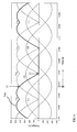
- the alternating supply voltage can be seen across the lower arm resistors as indicated in Figure 4 , where the sinusoidal signals represent the phase voltages U1, U2, U3 of the alternating supply voltage and the other signals the voltages across the resistors U R1 , U R2 , U R3 of corresponding phases respectively.
- the voltages of the resistors are measured in the potential of the lower DC-bus.
- Figure 8 shows the voltage waveforms across the resistors during the charging of the intermediate voltage circuit.
- the method of the invention thus requires that the voltage of the intermediate circuit is equal to or higher than the alternating supply voltage, since the upper free-wheeling diodes need to be in the blocking state as mentioned above.
- a voltage limit Vref is defined. This voltage limit is shown in Figure 4 . Further, the voltages U R1 , U R2 , U R3 produced by the alternating mains voltage and seen in the resistive circuits are compared with the voltage limit.
- Resistive circuits comprise resistive voltage divider circuits, i.e. at least two series-connected resistors. The purpose of the resistive circuit in connection with the invention is to produce a voltage that is proportional to the voltage of the alternating mains voltage, and, furthermore, to lower the voltage level suitable for control electronics.
- a first time instant T1 is determined when the voltage of any of the resistive circuits crosses the voltage limit.
- the voltages U R1 , U R2 , U R3 in all of the resistive circuits are compared with the voltage limit Vref and when one of the mentioned voltages crosses the limit the time instant of that crossing is determined.
- phase Since the procedure begins in a state where the rotational properties of the supply voltage are unknown, also the phase the voltage of which crossed the limit is determined. Each phase has a separate resistive circuit and the determination of the phase is thus a simple task. Also in connection with the crossing the direction of the crossing is determined. That is to say, it is determined, if the voltage that crossed the voltage limit had a rising or falling slope.
- the voltages of the resistive circuits are continuously monitored against the voltage limit after the first time instant.
- the second time instant T2 when the voltage of any of the resistive circuits crosses the voltage limit is also determined.
- the phase that crossed the voltage limit is also determined together with the direction of the crossing, similarly as in case of the first time instant.
- the phase sequence refers in a known manner to the direction of rotation.
- the phase sequence is determined based on the knowledge that all the three phases cross the voltage limit one after the other depending on the direction of the crossings, i.e. if the first phase that crosses the limit is U2 and the second phase is U1, then the next one will be U3. If, for example, this is the order of the first two crossings (U2, U1), then it can be determined that the next crossing will be from the voltage of phase U3.
- the compared voltages are the voltages from the resistive circuits, i.e. voltages U R1 , U R2 and U R3 . These voltages are derived directly from the alternating supply voltages (U1, U2 and U3) and therefore the order of the voltages in the resistive circuits gives the order of the phases.
- the direction of the third crossing is the same as that of the first one.
- the first and the third crossings having the same direction, the order of the phases is: the phase that crossed first, the phase that will cross third and the phase that crossed second.
- the phase sequence is thus U2, U3, U1.
- a peak time instant T12 is calculated.
- This peak time is a time instant in the middle of the first time instant T1 and second time instant T2. Due to the symmetry of the voltage curves, between every two consecutive crossings the third phase voltage has a peak value which is either negative or positive. Whether the peak is positive or negative can be determined from the direction of the first crossing that occurred at the first time instant. If the direction of the first crossing is such that the voltage goes below the voltage limit, then the peak voltage is positive. If, on the other hand, the direction of the first crossing is such that the voltage is rising, then the peak voltage is negative.
- Figure 5 illustrates a voltage space vector u , sometimes also called as space phasor.
- space vectors are rotating vectors in a complex plane that have a length and a direction.
- e j ⁇
- is the length of the space vector and ⁇ is the angle between the
- Figure 5 shows also the positive and negative phase sequences and the polarities of phase voltages. As known, the magnitudes of the phase voltages can be directly calculated from the rotating space vector.
- the angle of the rotating space vector is also known at that instant. It can be seen from Figure 5 that if, for example, phase U2 has a negative peak value at instant T12, then the angle of the voltage space vector is -60°.
- third time instant T3 is determined similarly as the first two instants.
- the first and third crossings have the same direction i.e. the voltage in the resistive circuit either rises or falls at both the first and third time instants.
- the frequency of the rotation of the alternating supply voltage is calculated from the first and third time instants.
- the time difference between the first and third time instants (T3 - T1) is one third of the full rotation of alternating supply.
- the time period for the full rotation of the alternating supply voltage is thus three times the said difference.
- the above embodiment determines the frequency quickly and is thus very usable when the mains side converter has to be synchronized with the alternating supply network quickly.
- the frequency of the supply network is calculated by measuring further time instants where any of the voltages of the resistive circuits crosses the voltage limit as described above. Then every other crossing time instant is selected and fed to a phase-locked loop, which determines the frequency. Every other crossing means, in principle, that either rising or falling voltage slopes are taken into account.
- the phase-locked loop outputs the information on the frequency
- the angle of the voltage of the supply network i.e. the angle of the space vector
- Angle t Angle ⁇ 12 + k ⁇ t - T ⁇ 12 ⁇ 2 ⁇ ⁇ f
- Angle12 is the angle of the space vector at the time instant T12
- k is a coefficient indicating the phase sequence, and its value is 1 when the phase sequence is positive and -1 when the phase sequence is negative.
- the angle of the alternating voltage can be calculated for example for synchronization purposes so that the converter control can be started.
- each of the voltages in the resistive circuits are A/D converted.
- the analogue signals are digitized and the maximum value of the conversion is then considered as the amplitude of the alternating line-to-line voltage.
- Figure 7 shows a dedicated measurement arrangement, in which the voltages of the resistive circuits are fed according to one embodiment of the invention.
- the voltages from the resistive circuits are fed to a common point through diodes D1, D2, D3.
- the basic rectifying function of the diodes D1, D2, D3 can be replaced with alternative circuit arrangements (e.g. operational amplifiers) that perform the same function.
- the voltage at the common point forms the voltage Umeas and it is basically the envelope of voltages in the resistive circuits U R1 , U R2 , U R3 .
- the amplitude of the mains voltage can be determined at a first possible instant using only one measurement. Fast voltage measurement is needed if the information of the amplitude is used for synchronization purposes and when the synchronization with the inverter is done after the third time instant.
- the voltage level of the supply network is known also beforehand.
- the measurement of the peak voltage gives the maximum line-to-line supply voltage from which the phase-to-neutral voltage can be obtained by dividing it by ⁇ 3.
- the voltage can also be easily determined from the converter DV-link voltage.
- the voltage limit Vref is adjustable.
- the adjustability of the voltage limit allows the method to be implemented in different situations. If it is foreseen that the mains voltage is high in amplitude, a higher voltage limit is also chosen, and, on the other hand, if the mains voltage amplitude is lower, a lower voltage limit should be chosen.
- the third reference crossing is noticed at time instant T3, where phase U1 goes below the voltage limit.
- the timer is read and the value is stored in T3.
- phase sequence is positive and thus k is 1.
- the converter can now start modulation and synchronize itself with the mains supply using this information.
- FIG. 6 shows similar voltage waveforms as Figure 4 .
- one of the voltages in the resistive circuits is selected to be the reference voltage to which other two voltages of the resistive circuits are compared.
- the first time instant and the second time instant are determined similarly as in the previously described embodiment. The difference is that the reference is not substantially constant, but is one of the voltages in the resistive circuits.
- the reference voltage is selected to be the voltage in the resistive circuit U R1 that is derived from the phase voltage U1 of the supply.
- a crossing takes place (time instants T1' and T2'), i.e. a voltage drops below or rises above the reference, it is known that at that moment the third phase has either a positive or a negative peak value.
- a third phase it is referred to that phase that is not the reference and not the voltage that crosses the reference.
- These phases are referred to as U not_crossT2 and U not_crossT1 at time instants T2' and T1', respectively.
- the phase in question is known.
- the direction (positive or negative) of the peak can also be directly determined. If the voltage in the resistive circuit of the phase that did not cross the reference voltage is higher than the reference voltage, then the peak is positive. And if the voltage in the resistive circuit of the phase that did not cross the reference voltage is lower than the reference voltage, the peak is negative.
- the information of the voltage of the third phase U not_crossT1 can be determined for example from the output of the comparator used in comparing the voltages.
- Angle t Angle ⁇ 1 + k * t - T ⁇ 1 ⁇ ⁇ * 2 * pi * f , where k is either -1 or 1 depending on the direction of rotation and Angle1 is the angle of the space vector at the first time instant T1'.
- U R1 is selected to be the reference voltage and it is thus derived directly from phase voltage U1 of the supply voltage.
- the phase that crosses the limit is phase U R2 .
- the third phase U not_crossT1 has a peak value at time instant T1'. Since voltage U R2 relating to phase U crosses the reference (U R1 ), the phase U3 has the peak value. At that moment U R3 is lower than the reference and thus the peak is negative.
- the angle of the voltage space vector at time instant T1' is 60°.
- phase U not_crossT2 is thus U2 and the voltage in the resistive circuit U R2 is higher than the reference and therefore phase U2 has a positive peak value at time instant T2'.
- the angle of the voltage space vector is now 120°. The vector has thus rotated in the positive direction.
- inventive concept can be implemented in various ways.
- inventive idea can be applied to other types of mains side converters, e.g. to so called Vienna rectifier.
- the invention and its embodiments are not limited to the examples described above but may vary within the scope of the claims.
Landscapes
- Engineering & Computer Science (AREA)
- Power Engineering (AREA)
- Inverter Devices (AREA)
- Rectifiers (AREA)
- Glass Compositions (AREA)
- Input Circuits Of Receivers And Coupling Of Receivers And Audio Equipment (AREA)
- Paper (AREA)
Abstract
Description
- The present invention relates to a method for determining properties of an alternating three-phase supply network, and particularly to a method with which a mains side converter of a frequency converter can be synchronized with the alternating three-phase supply network.
- A frequency converter consists of a mains side converter, an intermediate voltage circuit and an inverter. The mains side converter converts alternating input voltage to a DC-voltage of the intermediate voltage circuit also called as a DC-link. The voltage of the DC-link is further used for producing alternating voltage for the load. The alternating voltage is generated by using the inverter. Often it is also desirable to be able to feed power back to the supply network, or to control the reactive power drawn from the main or the improve the input power factor by shaping the input current, in which case the mains side converter can implemented with controllable switches and the structure of which is similar to that of the inverter.
- In a situation where the frequency converter is taken into use, the intermediate voltage circuit is without any charge thus the DC-voltage is zero. The capacitor of the DC-link has to be charged before any control operations can be carried out. Charging of the DC-link can be carried out for example by using the supply voltage connected to the DC-link via a charging resistor which limits the charging current from the supply. After the DC-link capacitor is charged to the normal operation value, the mains side converter has to be synchronized to the alternating voltage of the supply. This means that the properties, including frequency and phase sequence, of the alternating voltage have to be determined.
-
Figure 1 shows a simplified equivalent circuit of amains side converter 1 andalternating supply voltage 2 with phases U1, U2 and U3. InFigure 1 the mains side converter consists of active gate commutated semiconductor switches S11, S21, S31 in the upper branch and S12, S22, S32 in the lower branch, and parallel diodes D11, D21, D31 in the upper branch and D21, D22, D32 in the lower branch. The state information of the semiconductor switches, which is used for example to determine the switching time delays and possible malfunctions of the switches, is measured using high ohmic measurement resistor circuit R11, R12; R21, R22; R31, R32 in parallel with each of the semiconductor switching components in the lower branch. These resistor circuits inFigure 1 comprise two resistors in series and produce thus resistive voltage division of the voltage over the lower branch switches. It is clear, however, that resistive voltage division may comprise different number of resistances depending on the need. Further, inFigure 1 , afilter 3 is placed between the mains voltage and the converter. - When the active states of the converter switches are changed with some modulation scheme, the phase inputs of the converter are connected to either high intermediate voltage potential Udc+ or to low intermediate voltage potential Udc- through the controllable switches. The differing voltages between the supply and intermediate circuit can cause currents that may have very high values. In order to keep the currents in a tolerable range, the control system of the converter must be synchronized with its alternating three-phase supply voltage.
- Stable and smooth load control requires thus the converter control system to be synchronized with the alternating supply voltage. Synchronization is typically implemented with some sort of converter test voltage pulses applied to mains side of the converter, whose current response is measured and from this, the alternating voltage of the mains is approximated. International publication
WO 94/03965 - The above synchronization method requires switching of the active switches and also accurate and synchronized mains current measurements. Furthermore, the application of the first output voltage can lead to high currents if the direction and magnitude of the applied voltage is not chosen correctly.
- In some supply converters the phase currents are not directly measured due to the expenses of the current measurement elements. The current can be measured in normal operation for the purposes of converter control circuit using only one current measurement from the DC-intermediate circuit using a shunt resistor.
Figure 1 also includes shunt resistor Rshunt, the voltage over it being directly proportional to a current of one converter phase when one or two phases is connected to lower potential Udc- of the intermediate circuit, i.e. when either semiconductor switch or diode of the phase or phases in question are in a conductive state. - The usability of the above current measurement method is limited by the dependence between current information and usable switching states. If, for example, all phases of the converter are connected at the same time either to Udc+ or Udc- potential, there is no current through the shunt resistor although current is flowing in the phases of the supply voltage. This limitation due to the current measurement precludes the use of known synchronization methods, where test pulses are applied and the current response is measured.
- An object of the present invention is to provide a method so as to overcome the above problems relating to the synchronization of a mains side converter with a alternating voltage supply. The objects of the invention are achieved by a method which is characterized by what is stated in the independent claim. The preferred embodiments of the invention are disclosed in the dependent claims.
- The invention is based on the idea that the properties of alternating supply voltage can be determined by using resistors already present in the circuitry of a mains side converter. The determination of the properties is possible when the intermediate voltage of the frequency converter is equal to or higher than the line-to-line voltage of the supply voltage.
- An advantage of the method of the invention is that it is very simple in structure and it allows for a fast determination of the properties of the alternating supply network that are needed for full synchronization of the converter. The method requires only a minimal amount of additional elements and does not require the phase currents to be measured separately.
- In the following the invention will be described in greater detail by means of preferred embodiments with reference to the attached drawings, in which
-
Figure 1 is a simplified equivalent circuit of a mains side converter and an alternating three-phase supply network; -
Figures 2 and 3 show the voltage of the intermediate circuit during its charging; -
Figures 4 and6 show alternating mains voltages and the mains voltages in the converter; -
Figure 5 shows a voltage space vector diagram; -
Figure 7 shows an example of a circuit for determination of the alternating voltage magnitude; and -
Figure 8 shows the voltages in the resistive circuit during the charging of the intermediate circuit. -
Figure 1 shows an equivalent circuit of mains side converter and an alternating three-phase supply voltage connected to the converter. The converter feeds an intermediate voltage circuit providing voltages Udc+ and Udc- to the load, such as an inverter, which is not shown. InFigure 1 current is measured using a single shunt resistor Rshunt in the lower DC-bus. - The state of the converter active semiconductor switches is typically measured by using a resistive voltage division measurement across the lower arm IGBTs S12, S22, S32 and free-wheeling diodes D12, D22, D32 as shown in simplified schematic in
Figure 1 . This state information is used e.g. to approximate the commutation and switching delays. The same voltage measurement configuration can be used also for synchronization purposes according to the present invention. - When a frequency converter is started, the intermediate circuit has to be first charged. The charging can be carried out by placing a charging resistor in series with the capacitor of the intermediate circuit. Three-phase supply voltage then charges the capacitor through the free-wheeling diodes and the resistor. This voltage build-up is shown in
Figures 2 and 3 . -
Figure 2 shows the increasing voltage in a larger scale andFigure 3 is a partial reproduction ofFigure 2 at the time when the charging resistor is by-passed. InFigures 2 and 3 the charging resistor is by-passed approximately at t = 89ms, at which instant the voltage starts to increase more rapidly towards the value of rectified mains voltage. - As can be seen from the
Figures 2 and 3 , the voltage rises a little bit over the value of the rectified mains voltage due to inductances in the current path. This overshoot of voltage further means that the free-wheeling diodes D11, D21, D31, D12, D22, D32 of the mains side converter are in blocking state and there is no current flow in the main circuit due to the alternating supply voltage. However, the alternating supply voltage can be seen across the lower arm resistors as indicated inFigure 4 , where the sinusoidal signals represent the phase voltages U1, U2, U3 of the alternating supply voltage and the other signals the voltages across the resistors UR1, UR2, UR3 of corresponding phases respectively. The voltages of the resistors are measured in the potential of the lower DC-bus. -
Figure 8 shows the voltage waveforms across the resistors during the charging of the intermediate voltage circuit. The voltage waveforms are distorted until the time instant, when the charging resistor is by-passed and the voltage of the intermediate circuit has reached its operational value (approximately at t = 94ms). After that time instant the voltages in the resistive circuits are as indicated inFigures 4 and6 . - The method of the invention thus requires that the voltage of the intermediate circuit is equal to or higher than the alternating supply voltage, since the upper free-wheeling diodes need to be in the blocking state as mentioned above.
- At the beginning of the method of the invention the rotational state of the supply network or voltages of the alternating mains is unknown.
- In the method of the invention a voltage limit Vref is defined. This voltage limit is shown in
Figure 4 . Further, the voltages UR1, UR2, UR3 produced by the alternating mains voltage and seen in the resistive circuits are compared with the voltage limit. Resistive circuits comprise resistive voltage divider circuits, i.e. at least two series-connected resistors. The purpose of the resistive circuit in connection with the invention is to produce a voltage that is proportional to the voltage of the alternating mains voltage, and, furthermore, to lower the voltage level suitable for control electronics. - When the comparison between the voltages and the voltage limit has begun, a first time instant T1 is determined when the voltage of any of the resistive circuits crosses the voltage limit. The voltages UR1, UR2, UR3 in all of the resistive circuits are compared with the voltage limit Vref and when one of the mentioned voltages crosses the limit the time instant of that crossing is determined.
- Since the procedure begins in a state where the rotational properties of the supply voltage are unknown, also the phase the voltage of which crossed the limit is determined. Each phase has a separate resistive circuit and the determination of the phase is thus a simple task. Also in connection with the crossing the direction of the crossing is determined. That is to say, it is determined, if the voltage that crossed the voltage limit had a rising or falling slope.
- In the method of the invention the voltages of the resistive circuits are continuously monitored against the voltage limit after the first time instant. The second time instant T2 when the voltage of any of the resistive circuits crosses the voltage limit is also determined. The phase that crossed the voltage limit is also determined together with the direction of the crossing, similarly as in case of the first time instant.
- After these two time instants the phase sequence of the supply voltage can be determined. The phase sequence refers in a known manner to the direction of rotation. The phase sequence is determined based on the knowledge that all the three phases cross the voltage limit one after the other depending on the direction of the crossings, i.e. if the first phase that crosses the limit is U2 and the second phase is U1, then the next one will be U3. If, for example, this is the order of the first two crossings (U2, U1), then it can be determined that the next crossing will be from the voltage of phase U3. The compared voltages are the voltages from the resistive circuits, i.e. voltages UR1, UR2 and UR3. These voltages are derived directly from the alternating supply voltages (U1, U2 and U3) and therefore the order of the voltages in the resistive circuits gives the order of the phases.
- Since the consecutive crossings have different directions, the direction of the third crossing is the same as that of the first one. The first and the third crossings having the same direction, the order of the phases is: the phase that crossed first, the phase that will cross third and the phase that crossed second. In the above example the phase sequence is thus U2, U3, U1.
- According to the method of the invention, after the two time instants T1, T2 a peak time instant T12 is calculated. This peak time is a time instant in the middle of the first time instant T1 and second time instant T2. Due to the symmetry of the voltage curves, between every two consecutive crossings the third phase voltage has a peak value which is either negative or positive. Whether the peak is positive or negative can be determined from the direction of the first crossing that occurred at the first time instant. If the direction of the first crossing is such that the voltage goes below the voltage limit, then the peak voltage is positive. If, on the other hand, the direction of the first crossing is such that the voltage is rising, then the peak voltage is negative.
-
Figure 5 illustrates a voltage space vector u , sometimes also called as space phasor. As known in the art, space vectors are rotating vectors in a complex plane that have a length and a direction. A space vector for a variable x of a three phase system having phases a, b and c is constructed using equation
where
Figure 5 . -
Figure 5 shows also the positive and negative phase sequences and the polarities of phase voltages. As known, the magnitudes of the phase voltages can be directly calculated from the rotating space vector. - Since at time instant T12 one of the phase voltages has a positive or negative peak value, the angle of the rotating space vector is also known at that instant. It can be seen from
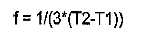
Figure 5 that if, for example, phase U2 has a negative peak value at instant T12, then the angle of the voltage space vector is -60°. - According to the method of the invention third time instant T3 is determined similarly as the first two instants. As already mentioned, the first and third crossings have the same direction i.e. the voltage in the resistive circuit either rises or falls at both the first and third time instants. In the preferred embodiment of the invention the frequency of the rotation of the alternating supply voltage is calculated from the first and third time instants. The time difference between the first and third time instants (T3 - T1) is one third of the full rotation of alternating supply. The time period for the full rotation of the alternating supply voltage is thus three times the said difference. Thus the electrical frequency f of the alternating supply voltage can be calculated as

- The above embodiment determines the frequency quickly and is thus very usable when the mains side converter has to be synchronized with the alternating supply network quickly.
- In another embodiment the frequency of the supply network is calculated by measuring further time instants where any of the voltages of the resistive circuits crosses the voltage limit as described above. Then every other crossing time instant is selected and fed to a phase-locked loop, which determines the frequency. Every other crossing means, in principle, that either rising or falling voltage slopes are taken into account. The phase-locked loop outputs the information on the frequency
- Now that the frequency, phase sequence and angle of the alternating supply network at time instant T12 are known, the angle of the voltage of the supply network, i.e. the angle of the space vector, can be calculated at a given time instant t with the following formula

where Angle12 is the angle of the space vector at the time instant T12 and k is a coefficient indicating the phase sequence, and its value is 1 when the phase sequence is positive and -1 when the phase sequence is negative. - With the above formula the angle of the alternating voltage can be calculated for example for synchronization purposes so that the converter control can be started.
- According to another embodiment each of the voltages in the resistive circuits are A/D converted. In the conversion the analogue signals are digitized and the maximum value of the conversion is then considered as the amplitude of the alternating line-to-line voltage.
-
Figure 7 shows a dedicated measurement arrangement, in which the voltages of the resistive circuits are fed according to one embodiment of the invention. In this embodiment the voltages from the resistive circuits are fed to a common point through diodes D1, D2, D3. The basic rectifying function of the diodes D1, D2, D3 can be replaced with alternative circuit arrangements (e.g. operational amplifiers) that perform the same function. The voltage at the common point forms the voltage Umeas and it is basically the envelope of voltages in the resistive circuits UR1, UR2, UR3. By measuring the envelope voltage the amplitude of the mains voltage can be determined at a first possible instant using only one measurement. Fast voltage measurement is needed if the information of the amplitude is used for synchronization purposes and when the synchronization with the inverter is done after the third time instant. Usually, the voltage level of the supply network is known also beforehand. - The measurement of the peak voltage gives the maximum line-to-line supply voltage from which the phase-to-neutral voltage can be obtained by dividing it by √3. The voltage can also be easily determined from the converter DV-link voltage.
- It is preferable that the voltage limit Vref is adjustable. The adjustability of the voltage limit allows the method to be implemented in different situations. If it is foreseen that the mains voltage is high in amplitude, a higher voltage limit is also chosen, and, on the other hand, if the mains voltage amplitude is lower, a lower voltage limit should be chosen.
- In the following, a simple sequence according to the invention is described with reference to
Figure 4 . First, the procedure is initialized for example in response to knowledge of the charged intermediate voltage circuit after a request made to a frequency converter to start the control of the mains side converter. First crossing of the limit voltage is noticed at time instant T1 where voltage UR3 drops below the limit voltage. A timer is started and T1 is set to zero. - Second limit voltage crossing is noticed at time instant T2, where voltage UR2 rises above the limit voltage. From the two crossings the phase sequence is known to be U1, U2, U3, phase U1 having a positive maximum between these two crossings. Since the positive maximum of phase U1 is referred to as zero angle for voltage space vector, the angle between the crossings is Angle12 = 0°. Timer is read and the value of T2 is determined. Now the time for the phase U1 positive maximum and for angle12 is calculated as T12 =(T2-T1)/2= T2/2.
- The third reference crossing is noticed at time instant T3, where phase U1 goes below the voltage limit. The timer is read and the value is stored in T3. Output frequency is calculated as f = 1/(3x(T3-T1) = 1/(3xT3). The voltage angle (in radians) at time instant T3 is also calculated as

- In this example the phase sequence is positive and thus k is 1.
- Now the rotation direction, frequency and absolute angle of the voltage vector are known. The converter can now start modulation and synchronize itself with the mains supply using this information.
- Another preferred embodiment of the invention is described with reference to
Figure 6 , which shows similar voltage waveforms asFigure 4 . In this embodiment one of the voltages in the resistive circuits is selected to be the reference voltage to which other two voltages of the resistive circuits are compared. In this embodiment the first time instant and the second time instant are determined similarly as in the previously described embodiment. The difference is that the reference is not substantially constant, but is one of the voltages in the resistive circuits. In the example ofFigure 6 the reference voltage is selected to be the voltage in the resistive circuit UR1 that is derived from the phase voltage U1 of the supply. - According to this embodiment, when a crossing takes place (time instants T1' and T2'), i.e. a voltage drops below or rises above the reference, it is known that at that moment the third phase has either a positive or a negative peak value. By a third phase it is referred to that phase that is not the reference and not the voltage that crosses the reference. These phases are referred to as Unot_crossT2 and Unot_crossT1 at time instants T2' and T1', respectively.
- It is thus already known that at time instant T1' one of the phases Unot_crossT1 has a peak value. Also the phase in question is known. The direction (positive or negative) of the peak can also be directly determined. If the voltage in the resistive circuit of the phase that did not cross the reference voltage is higher than the reference voltage, then the peak is positive. And if the voltage in the resistive circuit of the phase that did not cross the reference voltage is lower than the reference voltage, the peak is negative. The information of the voltage of the third phase Unot_crossT1 can be determined for example from the output of the comparator used in comparing the voltages. Thus already at the time instant T1' of the first crossing the angle of the voltage space vector is known.
- At the time instant of the second reference crossing, similar conclusions are made as at the first time instant. Thus the angle of the alternating voltage space vector is known at the second time instant T2'.
- Now two consecutive peaks are determined and thus the phase sequence can be determined. If the reference crossings have the same directions, i.e. the compared voltages rose above the reference at both time instants T1', T2' or the compared voltages dropped below the reference at both time instants T1', T2', then the frequency of the alternating supply voltage can be calculated as

- If, on the other hand, the directions of the two crossings are different (either up, down or down, up), then the frequency is calculated as

- Now the frequency, position and phase sequence are known and the angle of the space vector at any given time t can be calculated as

where k is either -1 or 1 depending on the direction of rotation and Angle1 is the angle of the space vector at the first time instant T1'. - Now referring more specifically to
Figure 6 , the following situation is considered. UR1 is selected to be the reference voltage and it is thus derived directly from phase voltage U1 of the supply voltage. After the beginning of the method the first reference crossing takes place at time instant T1'. The phase that crosses the limit is phase UR2. Thus the third phase Unot_crossT1 has a peak value at time instant T1'. Since voltage UR2 relating to phase U crosses the reference (UR1), the phase U3 has the peak value. At that moment UR3 is lower than the reference and thus the peak is negative. As shown inFigure 5 , the angle of the voltage space vector at time instant T1' is 60°. - Next, the following reference crossing takes place at time instant T2', where UR3 becomes higher than the reference. The third phase Unot_crossT2 is thus U2 and the voltage in the resistive circuit UR2 is higher than the reference and therefore phase U2 has a positive peak value at time instant T2'. The angle of the voltage space vector is now 120°. The vector has thus rotated in the positive direction.
- The consecutive crossings have same directions i.e, from below the reference to above it, and the frequency of the supply voltage can be calculated as f=1/(6*(T2'-T1')). Also the angle of the vector can be calculated as Angle(t) = 60° + (t-T1')*2*pi*f. The above embodiment is favourable since only two comparators are required for the method.
- It will be obvious to a person skilled in the art that, as the technology advances, the inventive concept can be implemented in various ways. The inventive idea can be applied to other types of mains side converters, e.g. to so called Vienna rectifier. The invention and its embodiments are not limited to the examples described above but may vary within the scope of the claims.
Claims (12)
- A method of determining a rotational state of a three-phase alternating supply voltage which is connected to a mains side converter, wherein the converter is connected to an intermediate voltage circuit (Udc+, Udc-) and comprises phase-specific upper and lower controllable switches (S11, S21, S31, S12, S22, S32), which are connected in series between the intermediate voltage circuit, free-wheeling diodes (D11, D21, D31, D12, D22, D32) connected in parallel with each of the controllable switches, and resistive circuits (R11, R12; R21, R22; R31, R32) connected in parallel with the lower controllable switches, characterized in that the method comprises the steps of selecting a voltage limit (Vref), comparing the voltages of the three-phase alternating supply in the resistive circuits (R11, R12; R21, R22; R31, R32) with the voltage limit (Vref), determining a first time instant (T1) when any of the voltages of the resistive circuits (R11, R12; R21, R22; R31, R32) crosses the voltage limit (Vref), determining a second time instant (T2) when any of the voltages of the resistive circuits (R11, R12; R21, R22; R31, R32) subsequently crosses the voltage limit (Vref), determining the phase sequence of the three-phase alternating supply voltage (U1, U2, U3) from the phases that crossed the voltage limit at the first and second time instants (T1, T2), determining the frequency of the three-phase alternating supply voltage from the determined time instants, the method being applicable when the voltage of the intermediate circuit is equal to or higher than the voltage of the three-phase alternating supply.
- A method according to claim 1, characterized in that the voltage limit is selected to be one of the voltages (UR1, UR2, UR3) produced by the alternating three-phase supply voltage in the resistive circuits (R11, R12; R21, R22; R31, R32), wherein the method comprises further steps of determining at the first time instant (T1) the phase (Unot_crossT1) that did not cross the voltage limit, this phase having a positive or negative peak value at the first time instant (T1), comparing the voltage of the resistive circuit of the determined phase (Unot_crossT1) with the voltage limit to determine if the peak is positive or negative, determining the angle (Angle1) of the alternating three-phase supply voltage space vector at the first time instant (T1), determining at the second time instant (T2) the phase (Unot_crossT2) that did not cross the voltage limit, this phase having a positive or negative peak value at the second time instant (T2), comparing the voltage of the resistive circuit of the determined phase (Unot_crossT2) with the voltage limit to determine if the peak is positive or negative, determining the angle (Angle2) of the alternating three-phase supply voltage space vector at the second time instant (T2).
- A method according to claim 2, characterized in that the peak value is determined to be a positive peak if the voltage in the resistive circuit of the phase that did not cross the voltage limit is higher than the voltage limit, and the peak value is determined to be a negative peak if the voltage in the resistive circuit of the phase that did not cross the voltage limit is lower than the voltage limit.
- A method according to claim 2 or 3, characterized in that the frequency of the alternating three-phase supply voltage is calculated as

- A method according to claim 1, characterized in that the method comprises the further steps of selecting the voltage limit to be a substantially constant value, determining the supply voltage phase (U1, U2, U3) the voltage of which crossed the voltage limit (Vref) at the first time instant (T1), determining the supply voltage phase (U1, U2, U3) the voltage of which crossed the voltage limit (Vref) at the second time instant (T2), determining the phase sequence of the alternating three-phase supply voltage phases (U1, U2, U3) from the phases that crossed the voltage limit at the first and second time instants (T1, T2), calculating a peak time instant (T12) which is in the middle of the first and second time instants (T1, T2), determining from the information of the supply voltage phases that crossed the voltage limit at the first and second time instants which output phase (U1, U2, U3) has a peak value at the peak time instant (T12), determining from the directions of the crossings whether the peak is a positive or a negative peak, determining a third time instant (T3) when any of the voltages of the resistive circuits subsequently crosses the voltage limit (Vref).
- A method according to claim 5, characterized in that the step of determining the frequency comprises the steps of calculating the frequency of the alternating three-phase supply voltage from the time difference between the first and third time instants.
- A method according to claim 5, characterized in that the step of determining the frequency comprises the steps of determining further time instants when any of the voltages of the resistive circuits crosses the voltage limit (Vref), selecting either time instants in which the voltage rises above the voltage limit or time instants in which the voltage drops below the voltage limit, and applying a phase-locked loop to the selected time instants, the output of which gives the frequency.
- A method according to any one of the previous claims 5 to 7, characterized in that the method further comprises the step of determining the magnitude of the supply voltage.
- A method according to claim 8, characterized in that the magnitude of the supply voltage is measured by measuring the voltages in the resistive circuits.
- A method according to claim 8, characterized in that the determination of the magnitude of the supply voltage comprises steps of feeding the voltages of the resistive circuits to a common point, and measuring the voltage of the common point.
- A method according to any one of the previous claims 5 to 10,
characterized in that the voltage limit is adjustable. - A method according to any one of the previous claims 2 to 11, characterized in that the method comprises a further step of calculating the voltage angle at a given time instant from the frequency, peak time instant and the phase sequence.
Priority Applications (3)
| Application Number | Priority Date | Filing Date | Title |
|---|---|---|---|
| EP07117326A EP2043239B1 (en) | 2007-09-27 | 2007-09-27 | Method in connection with mains side converter |
| DE602007004730T DE602007004730D1 (en) | 2007-09-27 | 2007-09-27 | Method for a converter connected to the supply network |
| AT07117326T ATE457545T1 (en) | 2007-09-27 | 2007-09-27 | METHOD FOR A POWER CONVERTER CONNECTED TO THE SUPPLY MAINS |
Applications Claiming Priority (1)
| Application Number | Priority Date | Filing Date | Title |
|---|---|---|---|
| EP07117326A EP2043239B1 (en) | 2007-09-27 | 2007-09-27 | Method in connection with mains side converter |
Publications (2)
| Publication Number | Publication Date |
|---|---|
| EP2043239A1 true EP2043239A1 (en) | 2009-04-01 |
| EP2043239B1 EP2043239B1 (en) | 2010-02-10 |
Family
ID=39227034
Family Applications (1)
| Application Number | Title | Priority Date | Filing Date |
|---|---|---|---|
| EP07117326A Not-in-force EP2043239B1 (en) | 2007-09-27 | 2007-09-27 | Method in connection with mains side converter |
Country Status (3)
| Country | Link |
|---|---|
| EP (1) | EP2043239B1 (en) |
| AT (1) | ATE457545T1 (en) |
| DE (1) | DE602007004730D1 (en) |
Cited By (1)
| Publication number | Priority date | Publication date | Assignee | Title |
|---|---|---|---|---|
| CN102299648A (en) * | 2010-06-28 | 2011-12-28 | 三菱电机株式会社 | Power converter |
Citations (4)
| Publication number | Priority date | Publication date | Assignee | Title |
|---|---|---|---|---|
| DE3236071A1 (en) * | 1982-07-09 | 1984-01-12 | Siemens AG, 1000 Berlin und 8000 München | Device for parallel supply into an AC or three-phase network |
| DE10048441A1 (en) | 2000-09-29 | 2002-05-02 | Siemens Ag | Detecting voltage breakdown in valve sections with series circuit of switchable power semiconductors, involves comparing voltage applied to each monitored valve section with threshold |
| US6459599B1 (en) * | 2001-06-01 | 2002-10-01 | Otis Elevator Company | Determining phase of AC mains in PWM controlled converters without voltage sensors |
| US20030075997A1 (en) | 2000-01-24 | 2003-04-24 | Keim Thomas A. | Alternator control circuit and related techniques |
-
2007
- 2007-09-27 DE DE602007004730T patent/DE602007004730D1/en active Active
- 2007-09-27 EP EP07117326A patent/EP2043239B1/en not_active Not-in-force
- 2007-09-27 AT AT07117326T patent/ATE457545T1/en not_active IP Right Cessation
Patent Citations (4)
| Publication number | Priority date | Publication date | Assignee | Title |
|---|---|---|---|---|
| DE3236071A1 (en) * | 1982-07-09 | 1984-01-12 | Siemens AG, 1000 Berlin und 8000 München | Device for parallel supply into an AC or three-phase network |
| US20030075997A1 (en) | 2000-01-24 | 2003-04-24 | Keim Thomas A. | Alternator control circuit and related techniques |
| DE10048441A1 (en) | 2000-09-29 | 2002-05-02 | Siemens Ag | Detecting voltage breakdown in valve sections with series circuit of switchable power semiconductors, involves comparing voltage applied to each monitored valve section with threshold |
| US6459599B1 (en) * | 2001-06-01 | 2002-10-01 | Otis Elevator Company | Determining phase of AC mains in PWM controlled converters without voltage sensors |
Cited By (4)
| Publication number | Priority date | Publication date | Assignee | Title |
|---|---|---|---|---|
| CN102299648A (en) * | 2010-06-28 | 2011-12-28 | 三菱电机株式会社 | Power converter |
| EP2400651A3 (en) * | 2010-06-28 | 2013-01-23 | Mitsubishi Electric Corporation | Power converter |
| US8773051B2 (en) | 2010-06-28 | 2014-07-08 | Mitsubishi Electric Corporation | Power converter |
| CN102299648B (en) * | 2010-06-28 | 2015-07-01 | 三菱电机株式会社 | Power converter |
Also Published As
| Publication number | Publication date |
|---|---|
| EP2043239B1 (en) | 2010-02-10 |
| ATE457545T1 (en) | 2010-02-15 |
| DE602007004730D1 (en) | 2010-03-25 |
Similar Documents
| Publication | Publication Date | Title |
|---|---|---|
| JP6490249B2 (en) | Power conversion device and power conversion system | |
| US7230837B1 (en) | Method and circuit for cascaded pulse width modulation | |
| US8319490B2 (en) | Method in connection with frequency converter | |
| US5481451A (en) | AC-to-AC power inverter apparatus functioning without smoothing capacitor, and control method thereof | |
| CN103185839B (en) | Permanent magnet motor inductance parameter measurement device and permanent magnet motor inductance parameter measurement method | |
| US5204606A (en) | Induction motor control apparatus | |
| US20030142517A1 (en) | Method for modulating pulse width, power converter, and inverter | |
| CN101682271A (en) | power conversion device | |
| JP6873251B2 (en) | Power converter and power conversion system | |
| US9742339B2 (en) | Apparatus for controlling inverter | |
| US5003455A (en) | Circuitry and method for controlling the firing of a thyristor | |
| US4829234A (en) | Method and apparatus for measuring the resistance of the winding of a converter-fed single- or three phase machine during operation | |
| CN104065294B (en) | A kind of method and control system for measuring phase current in polyphase inverter system | |
| Rahoui et al. | Frequency-adaptive neural network based virtual flux estimation for sensorless control of PWM converters under unbalanced conditions | |
| EP2043239B1 (en) | Method in connection with mains side converter | |
| Hingorani et al. | A new constant extinction angle control for ac/dc/ac static convertors | |
| JPH05232157A (en) | Voltage drop detection device | |
| Zhang et al. | Design and modelling of grid-connected PMSG-based wind energy conversion through diode rectifier, DC/DC and DC/AC converters | |
| US20140321179A1 (en) | Electrical Circuit Synchronisation | |
| US6563722B1 (en) | System and method for compensating for line imbalances in line commutated converters | |
| US6278623B1 (en) | System and method for compensating for voltage notches in two-phase phase locked loops | |
| JP5590106B2 (en) | Matrix converter | |
| KR101893240B1 (en) | Apparatus for controlling inverter | |
| JP5658995B2 (en) | Power converter and output voltage control method | |
| WO1995034125A1 (en) | A method for determining the rotational speed, magnitude and instantaneous direction of a flux |
Legal Events
| Date | Code | Title | Description |
|---|---|---|---|
| PUAI | Public reference made under article 153(3) epc to a published international application that has entered the european phase |
Free format text: ORIGINAL CODE: 0009012 |
|
| AK | Designated contracting states |
Kind code of ref document: A1 Designated state(s): AT BE BG CH CY CZ DE DK EE ES FI FR GB GR HU IE IS IT LI LT LU LV MC MT NL PL PT RO SE SI SK TR |
|
| AX | Request for extension of the european patent |
Extension state: AL BA HR MK RS |
|
| 17P | Request for examination filed |
Effective date: 20090708 |
|
| GRAP | Despatch of communication of intention to grant a patent |
Free format text: ORIGINAL CODE: EPIDOSNIGR1 |
|
| AKX | Designation fees paid |
Designated state(s): AT BE BG CH CY CZ DE DK EE ES FI FR GB GR HU IE IS IT LI LT LU LV MC MT NL PL PT RO SE SI SK TR |
|
| GRAS | Grant fee paid |
Free format text: ORIGINAL CODE: EPIDOSNIGR3 |
|
| GRAA | (expected) grant |
Free format text: ORIGINAL CODE: 0009210 |
|
| AK | Designated contracting states |
Kind code of ref document: B1 Designated state(s): AT BE BG CH CY CZ DE DK EE ES FI FR GB GR HU IE IS IT LI LT LU LV MC MT NL PL PT RO SE SI SK TR |
|
| REG | Reference to a national code |
Ref country code: GB Ref legal event code: FG4D |
|
| REG | Reference to a national code |
Ref country code: CH Ref legal event code: EP |
|
| REG | Reference to a national code |
Ref country code: IE Ref legal event code: FG4D |
|
| REF | Corresponds to: |
Ref document number: 602007004730 Country of ref document: DE Date of ref document: 20100325 Kind code of ref document: P |
|
| REG | Reference to a national code |
Ref country code: NL Ref legal event code: VDEP Effective date: 20100210 |
|
| LTIE | Lt: invalidation of european patent or patent extension |
Effective date: 20100210 |
|
| PG25 | Lapsed in a contracting state [announced via postgrant information from national office to epo] |
Ref country code: IS Free format text: LAPSE BECAUSE OF FAILURE TO SUBMIT A TRANSLATION OF THE DESCRIPTION OR TO PAY THE FEE WITHIN THE PRESCRIBED TIME-LIMIT Effective date: 20100610 Ref country code: ES Free format text: LAPSE BECAUSE OF FAILURE TO SUBMIT A TRANSLATION OF THE DESCRIPTION OR TO PAY THE FEE WITHIN THE PRESCRIBED TIME-LIMIT Effective date: 20100521 Ref country code: PT Free format text: LAPSE BECAUSE OF FAILURE TO SUBMIT A TRANSLATION OF THE DESCRIPTION OR TO PAY THE FEE WITHIN THE PRESCRIBED TIME-LIMIT Effective date: 20100611 Ref country code: LT Free format text: LAPSE BECAUSE OF FAILURE TO SUBMIT A TRANSLATION OF THE DESCRIPTION OR TO PAY THE FEE WITHIN THE PRESCRIBED TIME-LIMIT Effective date: 20100210 |
|
| PG25 | Lapsed in a contracting state [announced via postgrant information from national office to epo] |
Ref country code: PL Free format text: LAPSE BECAUSE OF FAILURE TO SUBMIT A TRANSLATION OF THE DESCRIPTION OR TO PAY THE FEE WITHIN THE PRESCRIBED TIME-LIMIT Effective date: 20100210 Ref country code: AT Free format text: LAPSE BECAUSE OF FAILURE TO SUBMIT A TRANSLATION OF THE DESCRIPTION OR TO PAY THE FEE WITHIN THE PRESCRIBED TIME-LIMIT Effective date: 20100210 Ref country code: LV Free format text: LAPSE BECAUSE OF FAILURE TO SUBMIT A TRANSLATION OF THE DESCRIPTION OR TO PAY THE FEE WITHIN THE PRESCRIBED TIME-LIMIT Effective date: 20100210 Ref country code: SI Free format text: LAPSE BECAUSE OF FAILURE TO SUBMIT A TRANSLATION OF THE DESCRIPTION OR TO PAY THE FEE WITHIN THE PRESCRIBED TIME-LIMIT Effective date: 20100210 |
|
| PG25 | Lapsed in a contracting state [announced via postgrant information from national office to epo] |
Ref country code: RO Free format text: LAPSE BECAUSE OF FAILURE TO SUBMIT A TRANSLATION OF THE DESCRIPTION OR TO PAY THE FEE WITHIN THE PRESCRIBED TIME-LIMIT Effective date: 20100210 Ref country code: SE Free format text: LAPSE BECAUSE OF FAILURE TO SUBMIT A TRANSLATION OF THE DESCRIPTION OR TO PAY THE FEE WITHIN THE PRESCRIBED TIME-LIMIT Effective date: 20100210 Ref country code: BE Free format text: LAPSE BECAUSE OF FAILURE TO SUBMIT A TRANSLATION OF THE DESCRIPTION OR TO PAY THE FEE WITHIN THE PRESCRIBED TIME-LIMIT Effective date: 20100210 Ref country code: CY Free format text: LAPSE BECAUSE OF FAILURE TO SUBMIT A TRANSLATION OF THE DESCRIPTION OR TO PAY THE FEE WITHIN THE PRESCRIBED TIME-LIMIT Effective date: 20100210 Ref country code: EE Free format text: LAPSE BECAUSE OF FAILURE TO SUBMIT A TRANSLATION OF THE DESCRIPTION OR TO PAY THE FEE WITHIN THE PRESCRIBED TIME-LIMIT Effective date: 20100210 Ref country code: GR Free format text: LAPSE BECAUSE OF FAILURE TO SUBMIT A TRANSLATION OF THE DESCRIPTION OR TO PAY THE FEE WITHIN THE PRESCRIBED TIME-LIMIT Effective date: 20100511 Ref country code: NL Free format text: LAPSE BECAUSE OF FAILURE TO SUBMIT A TRANSLATION OF THE DESCRIPTION OR TO PAY THE FEE WITHIN THE PRESCRIBED TIME-LIMIT Effective date: 20100210 |
|
| PG25 | Lapsed in a contracting state [announced via postgrant information from national office to epo] |
Ref country code: SK Free format text: LAPSE BECAUSE OF FAILURE TO SUBMIT A TRANSLATION OF THE DESCRIPTION OR TO PAY THE FEE WITHIN THE PRESCRIBED TIME-LIMIT Effective date: 20100210 Ref country code: CZ Free format text: LAPSE BECAUSE OF FAILURE TO SUBMIT A TRANSLATION OF THE DESCRIPTION OR TO PAY THE FEE WITHIN THE PRESCRIBED TIME-LIMIT Effective date: 20100210 Ref country code: BG Free format text: LAPSE BECAUSE OF FAILURE TO SUBMIT A TRANSLATION OF THE DESCRIPTION OR TO PAY THE FEE WITHIN THE PRESCRIBED TIME-LIMIT Effective date: 20100510 |
|
| PLBE | No opposition filed within time limit |
Free format text: ORIGINAL CODE: 0009261 |
|
| STAA | Information on the status of an ep patent application or granted ep patent |
Free format text: STATUS: NO OPPOSITION FILED WITHIN TIME LIMIT |
|
| 26N | No opposition filed |
Effective date: 20101111 |
|
| PG25 | Lapsed in a contracting state [announced via postgrant information from national office to epo] |
Ref country code: DK Free format text: LAPSE BECAUSE OF FAILURE TO SUBMIT A TRANSLATION OF THE DESCRIPTION OR TO PAY THE FEE WITHIN THE PRESCRIBED TIME-LIMIT Effective date: 20100210 |
|
| PG25 | Lapsed in a contracting state [announced via postgrant information from national office to epo] |
Ref country code: MC Free format text: LAPSE BECAUSE OF NON-PAYMENT OF DUE FEES Effective date: 20100930 |
|
| PG25 | Lapsed in a contracting state [announced via postgrant information from national office to epo] |
Ref country code: IE Free format text: LAPSE BECAUSE OF NON-PAYMENT OF DUE FEES Effective date: 20100927 |
|
| PG25 | Lapsed in a contracting state [announced via postgrant information from national office to epo] |
Ref country code: MT Free format text: LAPSE BECAUSE OF FAILURE TO SUBMIT A TRANSLATION OF THE DESCRIPTION OR TO PAY THE FEE WITHIN THE PRESCRIBED TIME-LIMIT Effective date: 20100210 |
|
| REG | Reference to a national code |
Ref country code: CH Ref legal event code: PL |
|
| PG25 | Lapsed in a contracting state [announced via postgrant information from national office to epo] |
Ref country code: CH Free format text: LAPSE BECAUSE OF NON-PAYMENT OF DUE FEES Effective date: 20110930 Ref country code: LI Free format text: LAPSE BECAUSE OF NON-PAYMENT OF DUE FEES Effective date: 20110930 |
|
| PG25 | Lapsed in a contracting state [announced via postgrant information from national office to epo] |
Ref country code: LU Free format text: LAPSE BECAUSE OF NON-PAYMENT OF DUE FEES Effective date: 20100927 Ref country code: HU Free format text: LAPSE BECAUSE OF FAILURE TO SUBMIT A TRANSLATION OF THE DESCRIPTION OR TO PAY THE FEE WITHIN THE PRESCRIBED TIME-LIMIT Effective date: 20100811 |
|
| PG25 | Lapsed in a contracting state [announced via postgrant information from national office to epo] |
Ref country code: TR Free format text: LAPSE BECAUSE OF FAILURE TO SUBMIT A TRANSLATION OF THE DESCRIPTION OR TO PAY THE FEE WITHIN THE PRESCRIBED TIME-LIMIT Effective date: 20100210 |
|
| PGFP | Annual fee paid to national office [announced via postgrant information from national office to epo] |
Ref country code: DE Payment date: 20140922 Year of fee payment: 8 Ref country code: FI Payment date: 20140911 Year of fee payment: 8 |
|
| PGFP | Annual fee paid to national office [announced via postgrant information from national office to epo] |
Ref country code: GB Payment date: 20140919 Year of fee payment: 8 Ref country code: FR Payment date: 20140919 Year of fee payment: 8 |
|
| PGFP | Annual fee paid to national office [announced via postgrant information from national office to epo] |
Ref country code: IT Payment date: 20140923 Year of fee payment: 8 |
|
| REG | Reference to a national code |
Ref country code: DE Ref legal event code: R119 Ref document number: 602007004730 Country of ref document: DE |
|
| PG25 | Lapsed in a contracting state [announced via postgrant information from national office to epo] |
Ref country code: IT Free format text: LAPSE BECAUSE OF NON-PAYMENT OF DUE FEES Effective date: 20150927 |
|
| GBPC | Gb: european patent ceased through non-payment of renewal fee |
Effective date: 20150927 |
|
| PG25 | Lapsed in a contracting state [announced via postgrant information from national office to epo] |
Ref country code: FI Free format text: LAPSE BECAUSE OF NON-PAYMENT OF DUE FEES Effective date: 20150927 |
|
| REG | Reference to a national code |
Ref country code: FR Ref legal event code: ST Effective date: 20160531 |
|
| PG25 | Lapsed in a contracting state [announced via postgrant information from national office to epo] |
Ref country code: GB Free format text: LAPSE BECAUSE OF NON-PAYMENT OF DUE FEES Effective date: 20150927 Ref country code: DE Free format text: LAPSE BECAUSE OF NON-PAYMENT OF DUE FEES Effective date: 20160401 |
|
| PG25 | Lapsed in a contracting state [announced via postgrant information from national office to epo] |
Ref country code: FR Free format text: LAPSE BECAUSE OF NON-PAYMENT OF DUE FEES Effective date: 20150930 |