EP2043025A1 - Radio frequency identification tag - Google Patents
Radio frequency identification tag Download PDFInfo
- Publication number
- EP2043025A1 EP2043025A1 EP08252823A EP08252823A EP2043025A1 EP 2043025 A1 EP2043025 A1 EP 2043025A1 EP 08252823 A EP08252823 A EP 08252823A EP 08252823 A EP08252823 A EP 08252823A EP 2043025 A1 EP2043025 A1 EP 2043025A1
- Authority
- EP
- European Patent Office
- Prior art keywords
- antenna
- rfid tag
- chip
- disk medium
- tag
- Prior art date
- Legal status (The legal status is an assumption and is not a legal conclusion. Google has not performed a legal analysis and makes no representation as to the accuracy of the status listed.)
- Withdrawn
Links
Images





Classifications
-
- G—PHYSICS
- G11—INFORMATION STORAGE
- G11B—INFORMATION STORAGE BASED ON RELATIVE MOVEMENT BETWEEN RECORD CARRIER AND TRANSDUCER
- G11B20/00—Signal processing not specific to the method of recording or reproducing; Circuits therefor
- G11B20/00086—Circuits for prevention of unauthorised reproduction or copying, e.g. piracy
-
- G—PHYSICS
- G06—COMPUTING OR CALCULATING; COUNTING
- G06K—GRAPHICAL DATA READING; PRESENTATION OF DATA; RECORD CARRIERS; HANDLING RECORD CARRIERS
- G06K19/00—Record carriers for use with machines and with at least a part designed to carry digital markings
- G06K19/06—Record carriers for use with machines and with at least a part designed to carry digital markings characterised by the kind of the digital marking, e.g. shape, nature, code
- G06K19/067—Record carriers with conductive marks, printed circuits or semiconductor circuit elements, e.g. credit or identity cards also with resonating or responding marks without active components
- G06K19/07—Record carriers with conductive marks, printed circuits or semiconductor circuit elements, e.g. credit or identity cards also with resonating or responding marks without active components with integrated circuit chips
-
- G—PHYSICS
- G06—COMPUTING OR CALCULATING; COUNTING
- G06K—GRAPHICAL DATA READING; PRESENTATION OF DATA; RECORD CARRIERS; HANDLING RECORD CARRIERS
- G06K19/00—Record carriers for use with machines and with at least a part designed to carry digital markings
- G06K19/04—Record carriers for use with machines and with at least a part designed to carry digital markings characterised by the shape
-
- G—PHYSICS
- G06—COMPUTING OR CALCULATING; COUNTING
- G06K—GRAPHICAL DATA READING; PRESENTATION OF DATA; RECORD CARRIERS; HANDLING RECORD CARRIERS
- G06K19/00—Record carriers for use with machines and with at least a part designed to carry digital markings
- G06K19/04—Record carriers for use with machines and with at least a part designed to carry digital markings characterised by the shape
- G06K19/041—Constructional details
- G06K19/042—Constructional details the record carrier having a form factor of a credit card and including a small sized disc, e.g. a CD or DVD
- G06K19/045—Constructional details the record carrier having a form factor of a credit card and including a small sized disc, e.g. a CD or DVD the record carrier being of the non-contact type, e.g. RFID, and being specially adapted for attachment to a disc, e.g. a CD or DVD
-
- G—PHYSICS
- G11—INFORMATION STORAGE
- G11B—INFORMATION STORAGE BASED ON RELATIVE MOVEMENT BETWEEN RECORD CARRIER AND TRANSDUCER
- G11B20/00—Signal processing not specific to the method of recording or reproducing; Circuits therefor
- G11B20/00086—Circuits for prevention of unauthorised reproduction or copying, e.g. piracy
- G11B20/00876—Circuits for prevention of unauthorised reproduction or copying, e.g. piracy wherein physical copy protection means are attached to the medium, e.g. holograms, sensors, or additional semiconductor circuitry
-
- G—PHYSICS
- G11—INFORMATION STORAGE
- G11B—INFORMATION STORAGE BASED ON RELATIVE MOVEMENT BETWEEN RECORD CARRIER AND TRANSDUCER
- G11B23/00—Record carriers not specific to the method of recording or reproducing; Accessories, e.g. containers, specially adapted for co-operation with the recording or reproducing apparatus ; Intermediate mediums; Apparatus or processes specially adapted for their manufacture
- G11B23/0014—Record carriers not specific to the method of recording or reproducing; Accessories, e.g. containers, specially adapted for co-operation with the recording or reproducing apparatus ; Intermediate mediums; Apparatus or processes specially adapted for their manufacture record carriers not specifically of filamentary or web form
- G11B23/0021—Record carriers not specific to the method of recording or reproducing; Accessories, e.g. containers, specially adapted for co-operation with the recording or reproducing apparatus ; Intermediate mediums; Apparatus or processes specially adapted for their manufacture record carriers not specifically of filamentary or web form discs
- G11B23/0028—Details
- G11B23/0035—Details means incorporated in the disc, e.g. hub, to enable its guiding, loading or driving
- G11B23/0042—Details means incorporated in the disc, e.g. hub, to enable its guiding, loading or driving with provision for auxiliary features
-
- G—PHYSICS
- G11—INFORMATION STORAGE
- G11B—INFORMATION STORAGE BASED ON RELATIVE MOVEMENT BETWEEN RECORD CARRIER AND TRANSDUCER
- G11B23/00—Record carriers not specific to the method of recording or reproducing; Accessories, e.g. containers, specially adapted for co-operation with the recording or reproducing apparatus ; Intermediate mediums; Apparatus or processes specially adapted for their manufacture
- G11B23/30—Record carriers not specific to the method of recording or reproducing; Accessories, e.g. containers, specially adapted for co-operation with the recording or reproducing apparatus ; Intermediate mediums; Apparatus or processes specially adapted for their manufacture with provision for auxiliary signals
Definitions
- the present invention relates to an RFID (Radio Frequency Identification) tag for wirelessly transmitting information such as ID (Identification) recorded in an IC chip.
- RFID Radio Frequency Identification
- An RFID tag comprises an IC chip and an antenna and can wirelessly transmit information such as an ID number recorded in the IC chip from the antenna. Accordingly, when communicating with the RFID tag using a reader/writer, information recorded in the IC chip can be read without contact. Thanks to radio transmission, information on IC chips can be read even in articles stored in a bag or box. Therefore, the RFID tag is widely used for manufacturing management and logistics of articles.
- CD Compact Disk
- DVD Digital Versatile Disk
- U.S. Patent 6,359,842 B1 discloses that when relative to the mass eccentricity due to the attaching of the IC chip to the disk, a balancer is provided at a position being point-symmetric to the IC chip with the center of the disk as the starting point, the amount of mass eccentricity is reduced.
- An RFID tag can be mounted on a disk medium by the technology described in U.S. Patent 6,359,842 B1 .
- a balancer must be prepared and extra operation such as provision of the balancer also occurs.
- the DVD having recorded thereon data on both surfaces of the disk medium it is difficult to attach the balancer on a data storage area as described in U.S. Patent 6,359,842 B1 .
- An example of the DVD is consistently one example, and the present invention described below can also be applied to the CD having recorded thereon data on one surface of the disk medium.
- a metal conductive layer such as Au or Al is used as a light reflection film.
- This metal conductive layer is normally formed on a substrate of the disk medium using an evaporation method or a sputtering technique.
- a formation range of the metal conductive layer is different for each application or manufacturer.
- the metal conductive layer is formed up to an edge of an opening in the center of the disk medium in some times.
- the present invention has been devised in the light of the above-described problems, and the amount of mass eccentricity due to the attachment of the RFID tag is reduced. Further, it is a preferred aim thereof to provide the RFID tag which may not depend on a structure of the disk medium and with which stable communication characteristics may be obtained.
- the RFID tag according to the present invention is an RFID tag having mounted thereon an IC chip capable of receiving and delivering information from and to an external source without contact.
- the central axis of the RFID tag is determined from the central axes of the IC chip, the antenna and the substrate, and the mass eccentricity is reduced by allowing the central axis of the RFID tag to coincide with the rotation axis of the disk medium.
- the adjustment of an antenna width also relates to the present invention.
- a position of the central axis may be required not only from structure of the disk media but also from design.
- An RFID tag according to the present invention is capable of receiving and delivering information from and to an IC chip without contact even if mounted on a high-speed rotating body.
- FIG. 1 shows an antenna of the circular RFID tag.
- an L-type slit 3 for performing impedance matching between an IC chip having recorded therein information and the antenna 1 is formed on this antenna 1.
- the IC chip 2 having recorded therein information is mounted on this antenna 1.
- There exists a center 5 being a center of a shape determined from a width and length of the antenna 1.
- a central axis of the antenna 1 having mounted thereon the IC chip 2 is located at a position shown in a central axis 4. When the antenna 1 is rotated around this central axis, a mass eccentricity can be canceled without using a balancer.
- the central axis used herein means an axis almost vertically penetrating an antenna surface via a center of gravity.
- a method of attaching the RFID tag on a rotating table and measuring by laser interferometry the amount of mass eccentricity at an end of the rotating table As another method, the measurement using a vibration sensor is used.
- FIG. 3A shows a construction view of the RFID tag and FIG. 3B shows a top plan view of the RFID tag.
- an appellation of the antenna such that the IC chip 2 is mounted on the antenna 1 described in FIG. 1 is defined as a tag antenna. That is, a reference numeral 7 shown in FIG. 3A depicts a tag antenna 7.
- a central axis of the tag antenna 7 is a central axis 4 and a central axis of the substrate 6 for retaining the tag antenna is a central axis 8.
- the substrate 6 shows a circular one; but is not limited thereto and may have an arbitrary shape. As shown in FIG.
- a notched region may be formed so as to be contacted with an opening in the substrate.
- an IC chip and an antenna may be directly formed on disk medium without using a substrate.
- the tag antenna 7 and the substrate 6 are arranged such that the central axes 4 and 8 of the tag antenna 7 and the substrate 6 coincide with each other and both are fixed with an adhesive or tacky adhesive.
- a film having laminated thereon a metal such as Al namely, an antenna material on a large film sheet or film tape-like substrate is coated with resist and then, antenna patterns are transferred to the film by a printing, a photolithography method or the like.
- an antenna pattern is formed by etching, and an IC chip is mounted.
- the desired RFID tag 9 with a shape of FIG. 3B can be manufactured.
- a protective film such as PP (Polypropylene) and PET (Polyethylene-terephthalate) is attached on an antenna surface. Accordingly, a structure of the RFID tag has a shape in which the protective film, IC chip, antenna, substrate and adhesive are laminated in this order and each thickness is 20, 50, 10, 20 and 10 ⁇ m.
- FIGS. 4A, 4B and 4C show tag shapes taking an attaching to the disk medium into consideration.
- FIG. 4A shows a top view of the RFID tag.
- An opening 10 is formed around the point in which the central axis 8A of the RFID tag shown in FIG. 3B and the center 11 of the RFID tag coincide with each other.
- FIG. 4B shows a cross sectional shape of the RFID tag taken along line IVB-IVB
- FIG. 4C shows a cross sectional shape of the RFID tag taken along line IVC-IVC.
- the opening 10 may be a non-penetrated hole.
- a position of the central axis may be marked to the extent to be recognized. In doing so, even in a rotating body incapable of attaching the RFID tag on the central axis, such as a gear, the RFID tag can also be attached on an end of the rotating axis of the rotating body.
- the RFID tag 9A shown in FIG. 5A depicts a tag in which the central axes of the tag antenna, the substrate and the center of an opening of the RFID tag coincide with each other.
- the RFID tag 9A is attached on the disk medium such that the center of an opening of the RFID tag 9A and that of the disk medium 12 coincide with each other.
- a tacky adhesive or adhesive As a tacky adhesive for use in the attachment, acrylic adhesive is frequently used. Since heat generation from the drive mechanism is large at the high speed rotation drive, when a tacky adhesive having high heat resistance is used, durability of the RFID tag can be more improved.
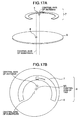
- each of the central axes of the IC chip, the antenna and the substrate may be deviated as shown in FIG. 17B .
- a combined central axis resulting from dynamically combining each of the central axes of the IC chip, the antenna and the substrate may substantially coincide with the center of the opening of the substrate or the rotation axis of the disk medium.
- the disk medium 12C shown in FIG. 6 has a fundamental structure common to general optical disk media such as the CD and DVD. More specifically, a central opening 13 is provided in the disk medium 12C and when the disk medium 12C is set in a player or disk drive, the disk medium 12C is rotated around the central opening 13 to irradiate an information recording surface of the disk with laser light, whereby signals are read out according to the quantity of light reflected from the surface. Further, in the outside area R1 as much as the prescribed distance from the central opening 13, a light reflecting film made of Au and Al is formed on a resin substrate, such as polycarbonate, being a substrate of the disk medium. This light reflecting film forms a thin film metal conductive layer having a thickness of several dozen nm.
- an area R2 that is a part of the area R1 having formed therein the metal conductive layer forms an information recording area.
- An area R4 serves as a clamping area and is an area in which a disk drive retains the disk medium.
- the metal conductive layer is not formed on the clamping area R4 in many cases.
- the metal conductive layer is increasingly formed also on the clamping area R4 in order to improve a design property on a label surface as a disk medium surface, in short, in order to have uniform gloss on a disk surface.
- An area R3 of the metal conductive layer within the clamping area R4 is different for each application or manufacturer.
- FIG. 7A shows a top plan view of a disk medium 12A in which a metal conductive layer 14A is not formed in the clamping area.
- FIGS. 7B and 7C show cross sectional structures taken along line VIIC-VIIC.
- FIG. 7B shows a case where the metal conductive layer 14A is formed between resin substrates 15A.
- FIG. 7C shows a case where the metal conductive layer 14A is formed on a resin substrate 15B.
- FIG. 7B shows a structure of the disk medium such as the DVD and
- FIG. 7C shows a structure of the disk medium such as the CD.
- a structure of FIG. 8 is the same as that of FIG. 7 , and FIG. 8 shows a structure of the disk medium in which the metal conductive layer 14B is formed up to the clamping area.
- the resin substrate 15B has a thickness of about 1.2 mm.
- the CD and DVD used at the moment each have a diameter of 120 mm.
- the area R1 having formed thereon the metal conductive layer has a diameter of 17 to 119 mm and the information recording area R2 in the area R1 has a diameter of 44 to 117 mm.
- the clamping area R4 has a diameter of 36 mm and the central opening 13 has a diameter of 15 mm.
- FIG. 8B shows a method of attaching the RFID tag on the disk medium 12B having a DVD structure and in which the metal conductive layer 14B is formed up to the clamping area.
- the metal conductive layer 14B is formed in the clamping area R4 having attached thereon the RFID tag. Accordingly, even if the RFID tag 9A described in the first embodiment is attached on the clamping area R4, the RFID tag cannot sufficiently respond to signals outputted from a reader due to the effect of the metal conductive layer 14B.
- the RFID tag can be operated by a method of inserting a spacer between the metal conductive layer and the RFID tag 9A.
- the RFID tag 9A becomes thicker and therefore, cannot be attached on the disk medium.
- the IC chip 2 when the IC chip 2 is mounted at a position at which lengths are different from each other in the lateral direction in an antenna having mounted thereon the IC chip 2, there is realized a tag antenna such that a relatively long communication distance is obtained even if the RFID tag is placed on the metal conductive layer of the disk medium.
- an antenna portion including the slit 33 is referred to as the first antenna and set to a portion with an antenna length of Ant 1 shown in the drawing.
- An antenna portion not including the slit 33 is referred to as the second antenna and set to a portion with an antenna length of Ant 2 shown in the drawing.
- each of the antennas is set such that the first antenna is equal in length to the second antenna.
- the antenna of this type is located near the metal conductive layer, the function of the antenna is deteriorated.
- each of the antennas is set such that the first antenna is shorter in length than the second antenna, and a length of the second antenna is set to an electrical length of ⁇ /2 ( ⁇ : wavelength) or to be approximated to an electrical length of ⁇ /2 at the operating frequency. Further, a length of the first antenna is set equal to or less than an electrical length of ⁇ /4 at the operating frequency.
- an electrical wavelength means a length in consideration of the effect of reduction in an antenna length due to the dielectric constant of a member on which the tag is attached.
- An antenna material used is Al with a thickness of 20 ⁇ m and a substrate material used is PEN (Poly Ethylene Naphthalate) with a thickness of 20 ⁇ m. These materials are not limited to the above description; further, if being antenna materials, materials for use in the RFID tag, such as Cu and Ag paste can be used. In the same manner, PET and paper can be used as the substrate material.
- the substrate has the effect as a spacer between the antenna and the metal conductive layer, and the effect of improving a communication distance in the structure of FIG. 8C typified by the CD.
- a central axis of the tag antenna is found and an opening is formed around the position in which the central axis of the tag antenna and the central axis of the substrate coincide with each other.
- An RFID tag 9C (not shown) coated with acrylic adhesive with a thickness of 10 ⁇ m is applied to the back side of the substrate of the RFID tag 9B (not shown) herein formed is prepared and attached onto a recording type DVD-R disk having formed thereon the metal conductive layer up to the clamping area R4.
- the communication distance of this RFID tag As the communication distance of this RFID tag, the communication distance of 100 mm from an attaching surface of the RFID tag and that of 40 mm from a back side of the disk medium are obtained on the condition that an operating frequency is 2.45 GHz, a high-frequency output is 200 mW, and a reader antenna 6dBi a patch antenna (circular polarization) is used.
- the RFID tag in which the mass eccentricity is canceled is realized by adjusting positions of the IC chip and tag antenna on the substrate, namely, by adjusting positions of these central axes.
- the mass eccentricity cannot be canceled, in some cases, in a correction processing only for adjusting a position of the central axis.
- the mass eccentricity is caused by the IC chip 32 attached on the antenna 31, the slit 33 and the gap 35 between the antenna ends.
- the mass eccentricity is caused by weight of the IC chip. Accordingly, when the weight of antenna materials around the IC chip 32 is reduced as much as that of the IC chip 32, the mass eccentricity due to the IC chip can be canceled.
- the slit 33 can be considered integrally with the IC chip. That is, since the slit 33 is formed by removing an antenna material, formation of the slit 33 acts in the direction of canceling the weight of the IC chip 32. A method of correcting the mass eccentricity through the antenna shapes will be described with reference to FIGS.
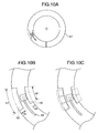
- FIG. 10A shows a top plan view of a tag antenna 17.
- FIG. 10B shows a detailed portion to be removed of the antenna material.
- FIG. 10C schematically shows the amount of the antenna material to be removed.
- a main constituent material of the IC chip is Si and a density thereof is 2.33 g/cm 3 .
- a density of Al of the antenna material is 2.7 g/cm 3 .
- Another antenna material includes Cu and a density thereof is 8.92 g/cm 3 .
- the area is 1.08 (mm 2 ).
- the area approximately corresponds to an area of four chips and corresponds to the removal of a part of the antenna, being 0.5 mm wide and about 2 mm long.
- antenna materials of an outer peripheral part 18 and an inner peripheral part 19 are removed from the open ring-shaped antenna having mounted thereon the IC chip.
- the mass eccentricity due to the IC chip can be substantially canceled.
- the antenna area is calculated.
- the antenna made of Cu has a thickness of 10 ⁇ m, the antenna area is equal to 0.0033 (mm 2 ).
- a material with a large density can correct the mass eccentricity by a small removal area.
- the circular tag antenna can be changed into a tag antenna having an open ring-shape with higher symmetry by using a method in which the central axis of the tag antenna coincides with the center of the RFID tag, as described in the first embodiment.
- FIG. 11 shows a variation in which a removal area 18A of the antenna is set to an outer peripheral portion of the antenna.
- a distance from the center of rotation becomes long. That is, when increasing, torque has an effect capable of reducing the removal area of the antenna.
- the mass eccentricity can be further corrected with higher accuracy by using a method in which the central axis of the tag antenna coincides with the center of the RFID tag, as described in the first embodiment.
- FIGS. 12A and 12B description will be made on an example in which the mass eccentricity of the tag antenna 90 shown in FIG. 9 is corrected with higher accuracy.
- the mass eccentricity due to the IC chip and the slit portion is taken notice of and corrected.
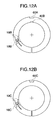
- FIGS. 12A and 12B show an example in which the gap 35 between the antenna ends shown in FIG. 9 is also taken notice of and corrected.
- the gap 35 is a portion in which the antenna material is absent. Accordingly, when removing the antenna material at a position being point-symmetric with respect to the rotation center, namely, at removal areas 60A and 60B, the mass eccentricity can be corrected.
- FIG. 12A shows an example in which the removal areas 60A and 60B are set in the inner peripheral side and the outer peripheral side of the antenna.
- FIG. 12B shows an example in which the removal area 60C is set in the outer peripheral side of the antenna.
- the mass eccentricity can be further corrected with higher accuracy by using at the same time a method in which the central axis of the tag antenna coincides with the center of the RFID tag, as described in the first embodiment.
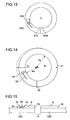
- the third variation shows a mode in which when removing the antenna material at a position being point-symmetric with respect to the rotation center, the mass eccentricity due to the gap 35 is corrected.
- the fourth variation shows a case in which when adding to the antenna ends the antenna material corresponding to the weight of the gap 35, the mass eccentricity is corrected.
- a correction method will be described.
- the fourth variation has a shape in which the antenna ends 61A and 61B are wider in width than the other antenna portions.
- the addition method of the antenna material to the outer peripheral side has an advantage in that a portion corresponding to the antenna ends 61A and 61B is reduced.
- the reading speed of the disk medium is increased and the number of rotations of the disk medium is increased and therefore, a reading error may be caused by vibrations due to the turbulence of air flow generated within the disk drive.
- description will be made on a structure of the RFID tag for preventing the turbulence of air flow generated within the disk drive.
- the RFID tag described in the first and the second embodiments has a structure in which the IC chip is formed on the disk medium.
- the RFID tag has a shape in which the IC chip has a thickness of 50 ⁇ m and only the IC chip having a protrusion with a height of 50 ⁇ m is formed on the antenna.
- a protective film is formed on the tag antenna; however, the periphery of the IC chip is projected.
- the disk medium rotates at high velocity, the turbulence of air flow is generated within the disk drive due to this protrusion and vibrations of the disk medium occur. As a result, the reading error is caused.
- the RFID tag has a structure in which the IC chip is prevented from being projected on the surface, that is, a structure in which a substrate 6 of the tag antenna faces outward as shown in FIG. 15 , the protrusion of the IC chip can be eliminated on the surface of the RFID tag.
- a surface of the RFID tag can be flattened.
- a material with a shape in which a hollow or hole for storing the IC chip is opened is used as this film.
- a resin such as PET, PEN and PP, or paper is used as this film.
- FIGS. 16A to 16D are process drawings showing a process for mounting the IC chip 2 on the feeding section of the antenna 41, in which FIG. 16A shows feeding sections of the antenna 41 and the IC chip 2, FIG. 16B shows a perspective enlarged view of the feeding section when mounting the IC chip 2 on the antenna 41, and FIG. 16C shows a cross sectional view of the junction between the antenna 41 and the IC chip 2.
- a key-like (L-shaped) slit 43 for performing the impedance matching between the IC chip 2 and the antenna 41 is formed on the feeding section of the antenna 41 and a portion surrounded by the key-like slit 43 is formed as a stub 41b. Further, in the IC chip 2, signal input/output electrodes 2a and 2b are formed at a distance to straddle the slit 43.
- a width of the slit 43 is somewhat narrower than a distance between signal input/output electrodes 2a and 2b of the IC chip 2. Therefore, as shown in FIG. 16B , when the IC chip 2 is mounted on the antenna 41, the signal input/output electrodes 2a and 2b of the IC chip 2 are connected to the antenna 41 so as to straddle the slit 43.
- a stub 41b formed by formation of the slit 43 is serially connected between the antenna 41 and the IC chip 2
- the stub 41b between the antenna 41 and the IC chip 2 operates as a serially connected inductance component. Accordingly, the input/output impedance between the antenna 41 and the IC chip 2 is matched due to this inductance component.
- a matching circuit is formed by the slit 43 and the stub 41b.
- the signal input/output electrodes 2a and 2b of the IC chip 2 is electrically joined to the antenna 41 using gold bump by an ultrasonic joining method, a metal eutectic joining method, or a joining method via an anisotropic conductive film (not shown).
- FIG. 16D is a conceptual diagram for mounting the IC chip 2 on a feeder section of the T shaped slit 43A in the antenna 41A.
- the impedance between the antenna 41A and the IC chip 2 can be matched in the same manner as in the case of the L shaped slit 43.
- the RFID tag according to the present embodiment is attached on a CD or DVD, the amount of mass eccentricity can be reduced, and therefore, the RFID tag can be read by a high-speed rotation type reader. Further, the RFID tag can be attached on the disk medium without regard to a forming position of the metal conductive layer of the CD or DVD. Accordingly, in a field of managing a large amount of disk media, information of each disk medium can be effectively managed, and further, management enhancement of recording media on sensitive information and personal information can be realized.
Landscapes
- Engineering & Computer Science (AREA)
- Physics & Mathematics (AREA)
- General Physics & Mathematics (AREA)
- Theoretical Computer Science (AREA)
- Computer Security & Cryptography (AREA)
- Signal Processing (AREA)
- Computer Hardware Design (AREA)
- Microelectronics & Electronic Packaging (AREA)
- Optical Record Carriers And Manufacture Thereof (AREA)
- Credit Cards Or The Like (AREA)
- Details Of Aerials (AREA)
Abstract

Description
- The present invention relates to an RFID (Radio Frequency Identification) tag for wirelessly transmitting information such as ID (Identification) recorded in an IC chip.
- An RFID tag comprises an IC chip and an antenna and can wirelessly transmit information such as an ID number recorded in the IC chip from the antenna. Accordingly, when communicating with the RFID tag using a reader/writer, information recorded in the IC chip can be read without contact. Thanks to radio transmission, information on IC chips can be read even in articles stored in a bag or box. Therefore, the RFID tag is widely used for manufacturing management and logistics of articles. In the management, the management of CD (Compact Disk), being an optical disk for use in music, or DVD (Digital Versatile Disk), being an optical disk for use in video, such as movies is included. In recent years, management enhancement of sensitive information and personal information is being promoted and the application of the RFID tag to disk media such as the CD and DVD having stored therein the information is being promoted. In reality, a data reading speed of these disk media increases and the rotation speed of the disk media exceeds 10000 rpm. It is needed to reduce the displacement of a center of gravity (hereinafter, referred to as a mass eccentricity) of the disk medium including the RFID tag.
-
U.S. Patent 6,359,842 B1 discloses that when relative to the mass eccentricity due to the attaching of the IC chip to the disk, a balancer is provided at a position being point-symmetric to the IC chip with the center of the disk as the starting point, the amount of mass eccentricity is reduced. - An RFID tag can be mounted on a disk medium by the technology described in
U.S. Patent 6,359,842 B1 . However, inU.S. Patent 6,359,842 B1 , a balancer must be prepared and extra operation such as provision of the balancer also occurs. In the technology disclosed inU.S. Patent 6,359,842 B1 , it is also difficult to attach the RFID tags on all of the currently distributed disk media. For example, in the DVD having recorded thereon data on both surfaces of the disk medium, it is difficult to attach the balancer on a data storage area as described inU.S. Patent 6,359,842 B1 . An example of the DVD is consistently one example, and the present invention described below can also be applied to the CD having recorded thereon data on one surface of the disk medium. - Further, for construction materials of the disk medium, a metal conductive layer such as Au or Al is used as a light reflection film. This metal conductive layer is normally formed on a substrate of the disk medium using an evaporation method or a sputtering technique. A formation range of the metal conductive layer is different for each application or manufacturer. In order that a design property on a label surface is improved in the DVD, being a disk medium for movie appreciation, the metal conductive layer is formed up to an edge of an opening in the center of the disk medium in some times. When these metal conductive layers come close to a tag antenna, electrical characteristics of the antenna deteriorate and a communication distance of the RFID tag is reduced. The above-described metal conductive layer has not received attention. Antenna characteristics change near the metal conductive layer and as a result, a desired communication distance cannot be obtained. Further, when the RFID tag is attached on the metal conductive layer, the antenna characteristics largely change and the RFID tag does not function as a practical RFID tag in many cases. This is a phenomenon in the same manner as in the case in which a general-purpose RFID tag is attached to a metal product. Therefore, the tag antenna is separated from the metal surface. That is, when taking measures to insert a thick spacer between the tag antenna and a metal member, the RFID tag can function as a practical RFID tag. However, when the RFID tag with the thick spacer is attached on the disk medium, the disk medium cannot be mounted on the disk drive in many cases, and therefore, the measures cannot be taken.
- The present invention has been devised in the light of the above-described problems, and the amount of mass eccentricity due to the attachment of the RFID tag is reduced. Further, it is a preferred aim thereof to provide the RFID tag which may not depend on a structure of the disk medium and with which stable communication characteristics may be obtained.
- For that purpose, the RFID tag according to the present invention is an RFID tag having mounted thereon an IC chip capable of receiving and delivering information from and to an external source without contact. In the RFID tag, the central axis of the RFID tag is determined from the central axes of the IC chip, the antenna and the substrate, and the mass eccentricity is reduced by allowing the central axis of the RFID tag to coincide with the rotation axis of the disk medium.
- Further, for the requirement of a position of the central axis due to the requirement in structure of the disk media, the adjustment of an antenna width also relates to the present invention. In addition, a position of the central axis may be required not only from structure of the disk media but also from design.
- An RFID tag according to the present invention is capable of receiving and delivering information from and to an IC chip without contact even if mounted on a high-speed rotating body.
- Other objects, features and advantages of the invention will become apparent from the following description of the embodiments of the invention taken in conjunction with the accompanying drawings.
IN THE DRAWINGS -
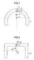
FIG. 1 is a top plan view of a circular tag antenna according to one embodiment of the present invention. -
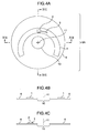
FIG. 2 is a top plan view of a rectangular tag antenna according to one embodiment of the present invention. -
FIGS. 3A and 3B are diagrams showing an RFID tag according to the first embodiment of the present invention, in whichFIG. 3A is a construction view, andFIG. 3B is a top plan view. -
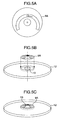
FIGS. 4A to 4C are diagrams showing the RFID tag according to the first embodiment of the present invention, in whichFIG. 4A is a top plan view, andFIGS. 4B and 4C are cross section views. -
FIGS. 5A to 5C are diagrams explaining the attaching of the RFID tag to a disk medium according to the first embodiment of the present invention. -
FIG. 6 is a schematic construction view of the disk medium. -
FIGS. 7A to 7C are diagrams explaining a structure of the disk medium. -
FIGS. 8A to 8C are diagrams explaining another structure of the disk medium. -
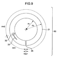
FIG. 9 is a top plan view of the tag antenna according to the second embodiment of the present invention. -
FIGS. 10A to 10C are top plan views of the tag antenna according to the second embodiment of the present invention. -
FIG. 11 is a top plan view of the tag antenna according to the second embodiment of the present invention (the second variation). -
FIGS. 12A and 12B are top plan views of the tag antenna according to the second embodiment of the present invention (the third variation). -
FIG. 13 is a top plan view of the tag antenna according to the second embodiment of the present invention (the fourth variation). -
FIG. 14 is a top plan view of the tag antenna according to the second embodiment of the present invention (the fifth variation). -
FIG. 15 is a cross section view showing the RFID tag according to the third embodiment of the present invention. -
FIGS. 16A to 16D are process drawings showing processes for mounting an IC chip on a feeder section of anantenna 41, in whichFIG. 16A shows feeder sections of the antenna and the IC chip,FIG. 16B is an enlarged view of the feeder section when the IC chip is mounted on the antenna,FIG. 16C shows cross sections of the antenna and the feeder section, andFIG. 16D is a conceptual diagram in which the IC chip is mounted on a feeder section of a T shaped slit. -
FIGS. 17A and 17B are diagrams showing the RFID tag according to the first embodiment of the present invention, in whichFIG. 17A is a construction view, andFIG. 17B is a top plan view. -
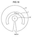
FIG. 18 is a diagram explaining a shape of a substrate. - With reference to the drawings, a preferred embodiment according to the best mode for carrying out the invention (hereinafter referred to as the embodiment) will be described below.
- First, an RFID according to the first embodiment will be described with reference to
FIG. 1. FIG. 1 shows an antenna of the circular RFID tag. On acircular antenna 1, an L-type slit 3 for performing impedance matching between an IC chip having recorded therein information and theantenna 1 is formed. TheIC chip 2 having recorded therein information is mounted on thisantenna 1. Description will be made later on the connection between theantenna 1 and theIC chip 2. There exists acenter 5 being a center of a shape determined from a width and length of theantenna 1. A central axis of theantenna 1 having mounted thereon theIC chip 2 is located at a position shown in acentral axis 4. When theantenna 1 is rotated around this central axis, a mass eccentricity can be canceled without using a balancer. The central axis used herein means an axis almost vertically penetrating an antenna surface via a center of gravity. - For measurement of the central axis, there is used a method of attaching the RFID tag on a rotating table and measuring by laser interferometry the amount of mass eccentricity at an end of the rotating table. As another method, the measurement using a vibration sensor is used.
- Further, in the same manner as in a rectangular antenna as shown in
FIG. 2 , when anIC chip 22 is mounted on anantenna 21 with an L-shapedslit 23, a center of the antenna is located in acenter 25. A central axis of theantenna 21 having mounted thereon theIC chip 22 is located at a position shown in a central axis 24. When theantenna 21 is rotated around this central axis, mass eccentricity does not exist. Accordingly, in a tag with an arbitrary shape, when the antenna is rotated around the central axis, the mass eccentricity can be canceled without using a balancer near the antenna. - Next, a method of forming the RFID tag according to the present embodiment will be described with reference to
FIGS. 3A and 3B. FIG. 3A shows a construction view of the RFID tag andFIG. 3B shows a top plan view of the RFID tag. First, an appellation of the antenna such that theIC chip 2 is mounted on theantenna 1 described inFIG. 1 is defined as a tag antenna. That is, areference numeral 7 shown inFIG. 3A depicts atag antenna 7. A central axis of thetag antenna 7 is acentral axis 4 and a central axis of thesubstrate 6 for retaining the tag antenna is acentral axis 8. Thesubstrate 6 shows a circular one; but is not limited thereto and may have an arbitrary shape. As shown inFIG. 18 , a notched region may be formed so as to be contacted with an opening in the substrate. Further, an IC chip and an antenna may be directly formed on disk medium without using a substrate. When forming the RFID tag, thetag antenna 7 and thesubstrate 6 are arranged such that thecentral axes tag antenna 7 and thesubstrate 6 coincide with each other and both are fixed with an adhesive or tacky adhesive. In a mass-production manner, as in a method of forming a general-purpose RFID tag, a film having laminated thereon a metal such as Al, namely, an antenna material on a large film sheet or film tape-like substrate is coated with resist and then, antenna patterns are transferred to the film by a printing, a photolithography method or the like. Further, an antenna pattern is formed by etching, and an IC chip is mounted. Next, when the RFID tag is processed by a punching operation around thecentral axis 4 of thetag antenna 7, the desiredRFID tag 9 with a shape ofFIG. 3B can be manufactured. For a product form of the RFID tag, a protective film such as PP (Polypropylene) and PET (Polyethylene-terephthalate) is attached on an antenna surface. Accordingly, a structure of the RFID tag has a shape in which the protective film, IC chip, antenna, substrate and adhesive are laminated in this order and each thickness is 20, 50, 10, 20 and 10 µm. - When a disk medium is set as an attaching object, the
RFID tag 9 must be mounted in conformity to an opening at the center of the disk medium.FIGS. 4A, 4B and 4C show tag shapes taking an attaching to the disk medium into consideration.FIG. 4A shows a top view of the RFID tag. Anopening 10 is formed around the point in which thecentral axis 8A of the RFID tag shown inFIG. 3B and thecenter 11 of the RFID tag coincide with each other. When theopening 10 has the same size as that in the opening of the disk medium or when theopening 10 is made larger than in size that of the disk medium, in mounting the disk medium on the disk drive, theopening 10 has an effect of preventing the RFID tag from being peeled off due to the contact with a spindle that is inserted into the opening.FIG. 4B shows a cross sectional shape of the RFID tag taken along line IVB-IVB andFIG. 4C shows a cross sectional shape of the RFID tag taken along line IVC-IVC. Here, theopening 10 may be a non-penetrated hole. Further, a position of the central axis may be marked to the extent to be recognized. In doing so, even in a rotating body incapable of attaching the RFID tag on the central axis, such as a gear, the RFID tag can also be attached on an end of the rotating axis of the rotating body. - A method of mounting the RFID tag on the disk medium will be described with reference to
FIGS. 5A to 5C . TheRFID tag 9A shown inFIG. 5A depicts a tag in which the central axes of the tag antenna, the substrate and the center of an opening of the RFID tag coincide with each other. As shown inFIG. 5B , theRFID tag 9A is attached on the disk medium such that the center of an opening of theRFID tag 9A and that of thedisk medium 12 coincide with each other. When theRFID tag 9A and thedisk medium 12 are fixed using a tacky adhesive or adhesive, a desired disk medium having mounted thereon theRFID tag 9A can be formed as shown inFIG. 5C . As a tacky adhesive for use in the attachment, acrylic adhesive is frequently used. Since heat generation from the drive mechanism is large at the high speed rotation drive, when a tacky adhesive having high heat resistance is used, durability of the RFID tag can be more improved. - In a method of taking the central axis according to the present embodiment, each of the central axes of the IC chip, the antenna and the substrate may be deviated as shown in
FIG. 17B . On this occasion, a combined central axis resulting from dynamically combining each of the central axes of the IC chip, the antenna and the substrate may substantially coincide with the center of the opening of the substrate or the rotation axis of the disk medium. - The
disk medium 12C shown inFIG. 6 has a fundamental structure common to general optical disk media such as the CD and DVD. More specifically, acentral opening 13 is provided in thedisk medium 12C and when thedisk medium 12C is set in a player or disk drive, thedisk medium 12C is rotated around thecentral opening 13 to irradiate an information recording surface of the disk with laser light, whereby signals are read out according to the quantity of light reflected from the surface. Further, in the outside area R1 as much as the prescribed distance from thecentral opening 13, a light reflecting film made of Au and Al is formed on a resin substrate, such as polycarbonate, being a substrate of the disk medium. This light reflecting film forms a thin film metal conductive layer having a thickness of several dozen nm. Further, an area R2 that is a part of the area R1 having formed therein the metal conductive layer forms an information recording area. An area R4 serves as a clamping area and is an area in which a disk drive retains the disk medium. Conventionally, the metal conductive layer is not formed on the clamping area R4 in many cases. In recent years, the metal conductive layer is increasingly formed also on the clamping area R4 in order to improve a design property on a label surface as a disk medium surface, in short, in order to have uniform gloss on a disk surface. An area R3 of the metal conductive layer within the clamping area R4 is different for each application or manufacturer. - Further, a forming position of the metal conductive layer on the resin substrate of the disk medium can be roughly classified.
FIG. 7A shows a top plan view of adisk medium 12A in which a metalconductive layer 14A is not formed in the clamping area.FIGS. 7B and 7C show cross sectional structures taken along line VIIC-VIIC.FIG. 7B shows a case where the metalconductive layer 14A is formed betweenresin substrates 15A.FIG. 7C shows a case where the metalconductive layer 14A is formed on aresin substrate 15B.FIG. 7B shows a structure of the disk medium such as the DVD andFIG. 7C shows a structure of the disk medium such as the CD. A structure ofFIG. 8 is the same as that ofFIG. 7 , andFIG. 8 shows a structure of the disk medium in which the metalconductive layer 14B is formed up to the clamping area. - When the disk medium is the CD, specifically, the
resin substrate 15B has a thickness of about 1.2 mm. When the disk medium is the DVD, theresin substrate 15A has a thickness of about 0.6 mm and the disk has a thickness of about 0.6 x 2=1.2 mm. - The CD and DVD used at the moment each have a diameter of 120 mm. The area R1 having formed thereon the metal conductive layer has a diameter of 17 to 119 mm and the information recording area R2 in the area R1 has a diameter of 44 to 117 mm. The clamping area R4 has a diameter of 36 mm and the
central opening 13 has a diameter of 15 mm. - The embodiment will be described on the case where the metal
conductive layer 14B serving as a light reflecting film is formed up to the clamping area of the disk medium as described above.FIG. 8B shows a method of attaching the RFID tag on thedisk medium 12B having a DVD structure and in which the metalconductive layer 14B is formed up to the clamping area. In the structure ofFIG. 8B , the metalconductive layer 14B is formed in the clamping area R4 having attached thereon the RFID tag. Accordingly, even if theRFID tag 9A described in the first embodiment is attached on the clamping area R4, the RFID tag cannot sufficiently respond to signals outputted from a reader due to the effect of the metalconductive layer 14B. This phenomenon is the same as that in the case where a general-purpose RFID tag is attached on a metallic article. Therefore, the RFID tag can be operated by a method of inserting a spacer between the metal conductive layer and theRFID tag 9A. However, theRFID tag 9A becomes thicker and therefore, cannot be attached on the disk medium. - In the following embodiment, when the
IC chip 2 is mounted at a position at which lengths are different from each other in the lateral direction in an antenna having mounted thereon theIC chip 2, there is realized a tag antenna such that a relatively long communication distance is obtained even if the RFID tag is placed on the metal conductive layer of the disk medium. With reference toFIG. 9 , description will be made on the RFID tag in which anIC chip 32 is mounted on an open ring-shapedtag antenna 31 and which operates on the metal conductive layer. Animpedance matching circuit 33 is formed in the open ring-shaped antenna with an inner radius R1, an outer radius R2, an antenna width (R2-R1) and a distance between antenna ends, namely, agap 35=Gap 1. With reference to a position at which theIC chip 32 is mounted, an antenna portion including theslit 33 is referred to as the first antenna and set to a portion with an antenna length ofAnt 1 shown in the drawing. An antenna portion not including theslit 33 is referred to as the second antenna and set to a portion with an antenna length ofAnt 2 shown in the drawing. In a normal dipole antenna, each of the antennas is set such that the first antenna is equal in length to the second antenna. However, when the antenna of this type is located near the metal conductive layer, the function of the antenna is deteriorated. In theantenna 31 ofFIG. 9 , each of the antennas is set such that the first antenna is shorter in length than the second antenna, and a length of the second antenna is set to an electrical length of λ/2 (λ: wavelength) or to be approximated to an electrical length of λ/2 at the operating frequency. Further, a length of the first antenna is set equal to or less than an electrical length of λ/4 at the operating frequency. Here, an electrical wavelength means a length in consideration of the effect of reduction in an antenna length due to the dielectric constant of a member on which the tag is attached. When the first antenna and the second antenna are not equal to each other, the second antenna is resonated through the first antenna. In this type, even if a distance between the tag antenna and the metal conductive layer varies, a change in the impedance of the tag antenna viewed from an input terminal of the IC chip, in other words, a change in the tuning frequency is extremely reduced. The fact corresponds to the presence or absence of the metal conductive layer under the tag antenna and has an advantage in that without regard to the structure of the disk medium, the RFID tag is attached on the disk media having different forming areas of the metal conductive layer described inFIGS. 7A to 7C and8A to 8C . - Specific sizes of the antenna of
FIG. 9 are as follows: R1=22 mm, R2=26 mm, an antenna width=2 mm, an outer peripheral length of Ant1=15 mm, an outer peripheral length of Ant2=65.6 mm, and Gap1=1 mm in a distance between antenna ends, namely,gap 35. An antenna material used is Al with a thickness of 20 µm and a substrate material used is PEN (Poly Ethylene Naphthalate) with a thickness of 20 µm. These materials are not limited to the above description; further, if being antenna materials, materials for use in the RFID tag, such as Cu and Ag paste can be used. In the same manner, PET and paper can be used as the substrate material. The substrate has the effect as a spacer between the antenna and the metal conductive layer, and the effect of improving a communication distance in the structure ofFIG. 8C typified by the CD. - Further, a central axis of the tag antenna is found and an opening is formed around the position in which the central axis of the tag antenna and the central axis of the substrate coincide with each other. The same process is performed also in the present embodiment. Since contents of this process are described in the first embodiment, a detailed description is omitted. An RFID tag 9C (not shown) coated with acrylic adhesive with a thickness of 10 µm is applied to the back side of the substrate of the RFID tag 9B (not shown) herein formed is prepared and attached onto a recording type DVD-R disk having formed thereon the metal conductive layer up to the clamping area R4. As the communication distance of this RFID tag, the communication distance of 100 mm from an attaching surface of the RFID tag and that of 40 mm from a back side of the disk medium are obtained on the condition that an operating frequency is 2.45 GHz, a high-frequency output is 200 mW, and a reader antenna 6dBi a patch antenna (circular polarization) is used.
- Next, a method of reducing the amount of mass eccentricity through antenna shapes will be described. In the first and the second embodiments, the RFID tag in which the mass eccentricity is canceled is realized by adjusting positions of the IC chip and tag antenna on the substrate, namely, by adjusting positions of these central axes. However, depending on types of the IC chip and antenna, the mass eccentricity cannot be canceled, in some cases, in a correction processing only for adjusting a position of the central axis.
- For example, suppose that when positions of the central axes coincide with each other in the heavy IC chip, the antenna partially mounts over the storage area of the disk medium. To cope with the above problem, description will be made on the method of reducing the amount of mass eccentricity through the antenna shapes using the following variations of five types.
- In a
tag antenna 90, the mass eccentricity is caused by theIC chip 32 attached on theantenna 31, theslit 33 and thegap 35 between the antenna ends. First, when theIC chip 32 is taken notice of, the mass eccentricity is caused by weight of the IC chip. Accordingly, when the weight of antenna materials around theIC chip 32 is reduced as much as that of theIC chip 32, the mass eccentricity due to the IC chip can be canceled. In the same manner, theslit 33 can be considered integrally with the IC chip. That is, since theslit 33 is formed by removing an antenna material, formation of theslit 33 acts in the direction of canceling the weight of theIC chip 32. A method of correcting the mass eccentricity through the antenna shapes will be described with reference toFIGS. 10A to 10C. FIG. 10A shows a top plan view of atag antenna 17.FIG. 10B shows a detailed portion to be removed of the antenna material.FIG. 10C schematically shows the amount of the antenna material to be removed. Assuming that a size of theIC chip 32 is 500 µm square, a thickness of the IC chip is 50 µm, and a thickness of Al of the antenna is 10 µm, the amount of the antenna to be removed is here calculated. A main constituent material of the IC chip is Si and a density thereof is 2.33 g/cm3. Further, a density of Al of the antenna material is 2.7 g/cm3. Another antenna material includes Cu and a density thereof is 8.92 g/cm3. The volume of theIC chip 32 is 0.5 x 0.5 x 0.05=0.0125(mm3), and the weight thereof is 29.1 µg. When converting the weight to an area of Al with a thickness of 10 µm, the area is 1.08 (mm2). When converting the area to an area of the IC chip, the area approximately corresponds to an area of four chips and corresponds to the removal of a part of the antenna, being 0.5 mm wide and about 2 mm long. Explaining this matter usingFIG. 10B , antenna materials of an outerperipheral part 18 and an innerperipheral part 19 are removed from the open ring-shaped antenna having mounted thereon the IC chip. Here, when the weight of Al materials corresponding to the range of L1 long and D1 wide and the range of L2 long and D2 wide is the same as that of the IC chip, the mass eccentricity due to the IC chip can be substantially canceled. In the same manner, when the antenna is made of Cu, the antenna area is calculated. When the antenna made of Cu has a thickness of 10 µm, the antenna area is equal to 0.0033 (mm2). As compared with Al, a material with a large density can correct the mass eccentricity by a small removal area. After the correction of the mass eccentricity, the circular tag antenna can be changed into a tag antenna having an open ring-shape with higher symmetry by using a method in which the central axis of the tag antenna coincides with the center of the RFID tag, as described in the first embodiment. -
FIG. 11 shows a variation in which aremoval area 18A of the antenna is set to an outer peripheral portion of the antenna. When the removal area is set only to the outer peripheral portion, a distance from the center of rotation becomes long. That is, when increasing, torque has an effect capable of reducing the removal area of the antenna. After the correction of the mass eccentricity, the mass eccentricity can be further corrected with higher accuracy by using a method in which the central axis of the tag antenna coincides with the center of the RFID tag, as described in the first embodiment. - With reference to
FIGS. 12A and 12B , description will be made on an example in which the mass eccentricity of thetag antenna 90 shown inFIG. 9 is corrected with higher accuracy. In the first and the second variations, the mass eccentricity due to the IC chip and the slit portion is taken notice of and corrected. Further,FIGS. 12A and 12B show an example in which thegap 35 between the antenna ends shown inFIG. 9 is also taken notice of and corrected. Thegap 35 is a portion in which the antenna material is absent. Accordingly, when removing the antenna material at a position being point-symmetric with respect to the rotation center, namely, atremoval areas FIG. 12A shows an example in which theremoval areas FIG. 12B shows an example in which theremoval area 60C is set in the outer peripheral side of the antenna. In the case ofFIG. 12B , since a distance from the rotation center increases, namely, the torque increases, the removal area of the antenna can be reduced. When an antenna width is narrow, a small removal amount is advantageous to the retainment of the antenna strength. After the correction of the mass eccentricity using the removal of the antenna member in the same manner as in the previous variation, the mass eccentricity can be further corrected with higher accuracy by using at the same time a method in which the central axis of the tag antenna coincides with the center of the RFID tag, as described in the first embodiment. - The third variation shows a mode in which when removing the antenna material at a position being point-symmetric with respect to the rotation center, the mass eccentricity due to the
gap 35 is corrected. The fourth variation shows a case in which when adding to the antenna ends the antenna material corresponding to the weight of thegap 35, the mass eccentricity is corrected. With reference toFIG. 13 , a correction method will be described. When in the circular antenna being discontinuous at thegap 35, the antenna material corresponding to the weight of thegap 35 is added to both of the antenna ends forming thegap 35, the mass eccentricity is corrected. Accordingly, the fourth variation has a shape in which the antenna ends 61A and 61B are wider in width than the other antenna portions. Further, when a distance from the rotation center, namely, the torque is considered, the addition method of the antenna material to the outer peripheral side has an advantage in that a portion corresponding to the antenna ends 61A and 61B is reduced. - With reference to
FIG. 14 , description will be made on a correction method in which a distance from the rotation center is used. Using as an example an open ring-shaped circular antenna with an inner radius of R3, when a distance from the rotation center is set to R4 smaller than R3, the torque of the IC chip is reduced and therefore, the mass eccentricity due to theIC chip 52 and theslit 53 can be canceled and the amount of the mass eccentricity can be reduced. When a distance from the rotation center corresponding to an inner radius of R4 increases, the correction can be performed relative to thegap 55. When the correction is further performed with high accuracy, the method according to the first embodiment in which the tag antenna is rotated around the central axis may be performed. - The reading speed of the disk medium is increased and the number of rotations of the disk medium is increased and therefore, a reading error may be caused by vibrations due to the turbulence of air flow generated within the disk drive. In the present embodiment, with reference to
FIG. 15 , description will be made on a structure of the RFID tag for preventing the turbulence of air flow generated within the disk drive. The RFID tag described in the first and the second embodiments has a structure in which the IC chip is formed on the disk medium. However, the RFID tag has a shape in which the IC chip has a thickness of 50 µm and only the IC chip having a protrusion with a height of 50 µm is formed on the antenna. A protective film is formed on the tag antenna; however, the periphery of the IC chip is projected. When the disk medium rotates at high velocity, the turbulence of air flow is generated within the disk drive due to this protrusion and vibrations of the disk medium occur. As a result, the reading error is caused. When the RFID tag has a structure in which the IC chip is prevented from being projected on the surface, that is, a structure in which asubstrate 6 of the tag antenna faces outward as shown inFIG. 15 , the protrusion of the IC chip can be eliminated on the surface of the RFID tag. More specifically, when attaching the RFID tag on the disk medium through an adhesive having the same thickness as that of theIC chip 32 on the antenna surface of the RFID tag or through a flatteningmaterial 70 such as a material which the adhesive is applied to each surface of a resin film, a surface of the RFID tag can be flattened. As the adhesive intervening between the disk medium and the RFID tag or the flatteningmaterial 70 serving as a film with an adhesive previously described, a material with a shape in which a hollow or hole for storing the IC chip is opened is used. A resin such as PET, PEN and PP, or paper is used as this film. Thereby, the turbulence of air flow generated within the disk drive can be reduced and the reading error at the high rotation velocity can be reduced. The method of correcting the mass eccentricity of the RFID tag used in the present embodiment is performed using the methods according to the first and the second embodiments previously described. - Description will be made in detail on a specific example in which a slit for impedance matching is provided in an
antenna 41 to mount theIC chip 2 thereon.FIGS. 16A to 16D are process drawings showing a process for mounting theIC chip 2 on the feeding section of theantenna 41, in whichFIG. 16A shows feeding sections of theantenna 41 and theIC chip 2,FIG. 16B shows a perspective enlarged view of the feeding section when mounting theIC chip 2 on theantenna 41, andFIG. 16C shows a cross sectional view of the junction between theantenna 41 and theIC chip 2. - As shown in
FIG. 16A , a key-like (L-shaped) slit 43 for performing the impedance matching between theIC chip 2 and theantenna 41 is formed on the feeding section of theantenna 41 and a portion surrounded by the key-like slit 43 is formed as astub 41b. Further, in theIC chip 2, signal input/output electrodes slit 43. - That is, a width of the
slit 43 is somewhat narrower than a distance between signal input/output electrodes IC chip 2. Therefore, as shown inFIG. 16B , when theIC chip 2 is mounted on theantenna 41, the signal input/output electrodes IC chip 2 are connected to theantenna 41 so as to straddle theslit 43. When astub 41b formed by formation of theslit 43 is serially connected between theantenna 41 and theIC chip 2, thestub 41b between theantenna 41 and theIC chip 2 operates as a serially connected inductance component. Accordingly, the input/output impedance between theantenna 41 and theIC chip 2 is matched due to this inductance component. In other words, a matching circuit is formed by theslit 43 and thestub 41b. As shown inFIG. 16C , the signal input/output electrodes IC chip 2 is electrically joined to theantenna 41 using gold bump by an ultrasonic joining method, a metal eutectic joining method, or a joining method via an anisotropic conductive film (not shown). - Further, the slit formed in the
antenna 41A can also be formed into not an L shape but a T shape.FIG. 16D is a conceptual diagram for mounting theIC chip 2 on a feeder section of the T shaped slit 43A in theantenna 41A. As shown inFIG. 16D , also when forming theslit 43A in theantenna 41A into a T shape and serially connecting thestubs IC chip 2 and theantenna 41A, the impedance between theantenna 41A and theIC chip 2 can be matched in the same manner as in the case of the L shaped slit 43. - Also when the RFID tag according to the present embodiment is attached on a CD or DVD, the amount of mass eccentricity can be reduced, and therefore, the RFID tag can be read by a high-speed rotation type reader. Further, the RFID tag can be attached on the disk medium without regard to a forming position of the metal conductive layer of the CD or DVD. Accordingly, in a field of managing a large amount of disk media, information of each disk medium can be effectively managed, and further, management enhancement of recording media on sensitive information and personal information can be realized.
- It should be further understood by those skilled in the art that although the foregoing description has been made on embodiments of the invention, the invention is not limited thereto and various changes and modifications may be made without departing from the spirit of the invention and the scope of the appended claims, as interpreted by the description and drawings.
Claims (15)
- An RFID tag (9), comprising:an antenna (1);an IC chip (2); anda substrate (6), whereininformation recorded in the IC chip (2) is wirelessly transmitted, anda central axis (8A) of the RFID tag (9) and a center of an opening (10) of the substrate (6) coincide with each other.
- The RFID tag (9) according to claim 1, wherein a position of each central axis of the antenna (1), the IC chip (2) and the substrate (6) coincides with each other to locate a central axis (8A) of the RFID tag (9).
- The RFID tag (9) according to claim 2, wherein
the IC chip (2) is connected to the antenna (1); and
a width of the antenna (1) near an area in which the IC chip (2) is connected to the antenna (1) is narrower than that in the other area. - The RFID tag according (9) to claim 2, wherein
the antenna (1) is substantially a circular ring with a notch; and
a width of the antenna (1) in an area at a position being point-symmetric to the notch with respect to a center of an opening (10) of the substrate (6) is narrower than that in the other area. - The RFID tag (9) according to claim 2, wherein
the antenna (1) is substantially a circular ring with the notch, and
ends (61A, 61B) of the antenna (1) are wider in width than the other portion of the antenna (1). - The RFID tag (9) according to claim 2, wherein
the antenna (1) includes a first antenna (Ant1) and a second antenna (Ant2) whose lengths are different from each other, and the IC chip (2) is mounted on a boundary of the first and the second antennas. - The RFID tag (9) according to claim 6, wherein
when a wavelength of an operating frequency is set to λ, an electric length of the first antenna (Ant1) is equal to or less than λ/4. - The RFID tag (9) according to claim 6, wherein
when a wavelength of an operating frequency is set to λ, an electric length of the second antenna (Ant2) is equal to λ/2. - A disk medium (12) having an antenna (1) for wirelessly transmitting information recorded in an IC chip (2), wherein
a combined center of gravity of the antenna (1) and the IC chip (2), and a rotation axis of the disk medium (12) coincide with each other. - The disk medium (12) according to claim 9, wherein
the antenna (1) and the IC chip (2) are arranged such that each central axis thereof coincides with a rotation axis of the disk medium (12). - The disk medium (12) according to claim 10, wherein
a width of an antenna (1) near an area on which the IC chip (2) is mounted on the antenna (1) is narrower than that in the other area. - The disk medium (12) according to claim 10, wherein
the antenna (1) is substantially a circular ring with a notch, and
a width of the antenna (1) in an area at a position being point-symmetric to the notch with respect to a rotation axis of the disk medium (12) is narrower than that in the other area. - The disk medium (12) according to claim 10, wherein
the antenna (1) is substantially a circular ring with the notch, and
ends (61A, 61B) of the antenna are wider in width than the other portion of the antenna (1). - The disk medium (12) according to claim 10, wherein the antenna (1) includes a first antenna (Ant1) and a second antenna (Ant2) whose lengths are different from each other, and the IC chip (2) is mounted on a boundary of the first and the second antennas.
- The disk medium (12) according to claim 14, wherein when a wavelength of an operating frequency is set to λ, an electric length of the first antenna (Ant1) is equal to or less than λ/4 and an electric length of the second antenna (Ant2) is equal to λ/2.
Applications Claiming Priority (1)
| Application Number | Priority Date | Filing Date | Title |
|---|---|---|---|
| JP2007253027A JP5065833B2 (en) | 2007-09-28 | 2007-09-28 | RFID tag |
Publications (1)
| Publication Number | Publication Date |
|---|---|
| EP2043025A1 true EP2043025A1 (en) | 2009-04-01 |
Family
ID=39968054
Family Applications (1)
| Application Number | Title | Priority Date | Filing Date |
|---|---|---|---|
| EP08252823A Withdrawn EP2043025A1 (en) | 2007-09-28 | 2008-08-26 | Radio frequency identification tag |
Country Status (6)
| Country | Link |
|---|---|
| US (1) | US8098133B2 (en) |
| EP (1) | EP2043025A1 (en) |
| JP (1) | JP5065833B2 (en) |
| KR (1) | KR101054182B1 (en) |
| CN (1) | CN101398911A (en) |
| TW (1) | TWI409704B (en) |
Cited By (2)
| Publication number | Priority date | Publication date | Assignee | Title |
|---|---|---|---|---|
| CN107342461A (en) * | 2017-07-04 | 2017-11-10 | 北京邮电大学 | A kind of uhf band RFID arrowbands trap mask |
| CN111211399A (en) * | 2020-03-04 | 2020-05-29 | 电子科技大学 | A metal-resistant ultra-high frequency electronic tag antenna conforming to the wall of the oil pipe casing |
Families Citing this family (14)
| Publication number | Priority date | Publication date | Assignee | Title |
|---|---|---|---|---|
| TW200935315A (en) * | 2008-02-01 | 2009-08-16 | Taiwan Name Plate Co Ltd | An ordering catalog with electronic bookmarks |
| US8249263B2 (en) * | 2008-05-15 | 2012-08-21 | International Business Machines Corporation | Method and apparatus for providing audio motion feedback in a simulated three-dimensional environment |
| US8493188B2 (en) * | 2009-01-14 | 2013-07-23 | International Business Machines Corporation | Haptic motion feedback device |
| US8344861B2 (en) * | 2009-01-14 | 2013-01-01 | International Business Machines Corporation | Haptic motion feedback mechanism |
| JP5671874B2 (en) | 2009-12-28 | 2015-02-18 | 富士通株式会社 | Wireless tag |
| US9760750B1 (en) * | 2015-01-12 | 2017-09-12 | The United States Of America As Represented By The Administrator Of The National Aeronautics And Space Administration | System for RFID-enabled information collection |
| CN106785352B (en) * | 2016-12-30 | 2023-08-25 | 歌尔科技有限公司 | Mobile phone antenna and mobile phone thereof |
| US10776682B2 (en) | 2016-12-30 | 2020-09-15 | Hong Kong R&D Centre for Logistics and Supply Chain Management Enabling Technologies Limited | Switchable RFID tag and a method for operating a switchable RFID circuit |
| DE102017104046A1 (en) * | 2017-02-27 | 2018-08-30 | Infineon Technologies Ag | NEAR FIELD COMMUNICATION-RING |
| CN107194454A (en) * | 2017-05-26 | 2017-09-22 | 宝钢轧辊科技有限责任公司 | RFID chip and its Sendzimir roll identification with managerial application |
| CN109754053A (en) * | 2018-12-17 | 2019-05-14 | 广东工业大学 | Miniaturized high-gain anti-metal tag antenna based on dielectric resonator |
| CN110703000B (en) * | 2019-08-26 | 2021-12-03 | 中汽研汽车检验中心(天津)有限公司 | Eccentricity correction method applied to automobile antenna performance test |
| WO2021061122A1 (en) * | 2019-09-25 | 2021-04-01 | Hewlett-Packard Development Company, L.P. | Developer roller authentication |
| CN113421389B (en) * | 2021-06-23 | 2022-08-12 | 深圳市中天迅通信技术股份有限公司 | Antenna device for POS machine |
Citations (4)
| Publication number | Priority date | Publication date | Assignee | Title |
|---|---|---|---|---|
| WO1999038162A1 (en) * | 1998-01-22 | 1999-07-29 | Nds Ltd. | Protection of data on media recording disks |
| US6359842B1 (en) | 1998-10-22 | 2002-03-19 | Hitachi, Ltd. | Disc having a semiconductor memory |
| WO2004107261A1 (en) * | 2003-05-29 | 2004-12-09 | Finanziaria Sammarinese, S.A. | Optical read disk and production method for the same |
| US20060028344A1 (en) * | 2003-04-25 | 2006-02-09 | Forster Ian J | Extended range RFID system |
Family Cites Families (13)
| Publication number | Priority date | Publication date | Assignee | Title |
|---|---|---|---|---|
| JP2000132871A (en) * | 1998-10-22 | 2000-05-12 | Hitachi Ltd | Disc and recording / reproducing apparatus using the same |
| JP2000268415A (en) * | 1999-03-16 | 2000-09-29 | Rohm Co Ltd | Disc-shaped record carrier |
| JP3746396B2 (en) * | 1999-04-27 | 2006-02-15 | 富士通株式会社 | Output circuit and input / output circuit |
| JP2001297568A (en) | 2000-04-12 | 2001-10-26 | Mitsubishi Materials Corp | Index device, recording medium with index for storing table of contents used in this device, and its RFID |
| JP3713476B2 (en) * | 2002-09-10 | 2005-11-09 | 株式会社東芝 | Mobile communication terminal |
| JP2005190514A (en) * | 2003-12-24 | 2005-07-14 | Dainippon Printing Co Ltd | Digital recording medium and reproducing apparatus |
| KR100603761B1 (en) * | 2004-04-22 | 2006-07-24 | 삼성전자주식회사 | Microwave transponder |
| JP4328682B2 (en) | 2004-07-13 | 2009-09-09 | 富士通株式会社 | Radio tag antenna structure for optical recording medium and optical recording medium housing case with radio tag antenna |
| JP2006092630A (en) * | 2004-09-22 | 2006-04-06 | Sony Corp | Optical disc and manufacturing method thereof |
| JP4639857B2 (en) * | 2005-03-07 | 2011-02-23 | 富士ゼロックス株式会社 | A storage box for storing articles to which RFID tags are attached, an arrangement method thereof, a communication method, a communication confirmation method, and a packaging structure. |
| TWI339358B (en) * | 2005-07-04 | 2011-03-21 | Hitachi Ltd | Rfid tag and manufacturing method thereof |
| EP1913530B1 (en) * | 2005-08-02 | 2014-10-08 | Nxp B.V. | Antenna structure, transponder and method of manufacturing an antenna structure |
| JP4200464B2 (en) * | 2006-08-04 | 2008-12-24 | ソニー株式会社 | Molded body and manufacturing method thereof |
-
2007
- 2007-09-28 JP JP2007253027A patent/JP5065833B2/en not_active Expired - Fee Related
-
2008
- 2008-08-06 CN CNA2008101313402A patent/CN101398911A/en active Pending
- 2008-08-06 TW TW097129874A patent/TWI409704B/en not_active IP Right Cessation
- 2008-08-07 KR KR1020080077378A patent/KR101054182B1/en not_active Expired - Fee Related
- 2008-08-26 EP EP08252823A patent/EP2043025A1/en not_active Withdrawn
- 2008-08-28 US US12/200,349 patent/US8098133B2/en not_active Expired - Fee Related
Patent Citations (4)
| Publication number | Priority date | Publication date | Assignee | Title |
|---|---|---|---|---|
| WO1999038162A1 (en) * | 1998-01-22 | 1999-07-29 | Nds Ltd. | Protection of data on media recording disks |
| US6359842B1 (en) | 1998-10-22 | 2002-03-19 | Hitachi, Ltd. | Disc having a semiconductor memory |
| US20060028344A1 (en) * | 2003-04-25 | 2006-02-09 | Forster Ian J | Extended range RFID system |
| WO2004107261A1 (en) * | 2003-05-29 | 2004-12-09 | Finanziaria Sammarinese, S.A. | Optical read disk and production method for the same |
Cited By (2)
| Publication number | Priority date | Publication date | Assignee | Title |
|---|---|---|---|---|
| CN107342461A (en) * | 2017-07-04 | 2017-11-10 | 北京邮电大学 | A kind of uhf band RFID arrowbands trap mask |
| CN111211399A (en) * | 2020-03-04 | 2020-05-29 | 电子科技大学 | A metal-resistant ultra-high frequency electronic tag antenna conforming to the wall of the oil pipe casing |
Also Published As
| Publication number | Publication date |
|---|---|
| TWI409704B (en) | 2013-09-21 |
| TW200926005A (en) | 2009-06-16 |
| KR101054182B1 (en) | 2011-08-03 |
| CN101398911A (en) | 2009-04-01 |
| US20090085751A1 (en) | 2009-04-02 |
| JP5065833B2 (en) | 2012-11-07 |
| US8098133B2 (en) | 2012-01-17 |
| JP2009086799A (en) | 2009-04-23 |
| KR20090032954A (en) | 2009-04-01 |
Similar Documents
| Publication | Publication Date | Title |
|---|---|---|
| US8098133B2 (en) | Radio frequency identification tag | |
| JP4437965B2 (en) | Wireless tag | |
| US7248221B2 (en) | Radio tag antenna structure for an optical recording medium and a case for an optical recording medium with a radio tag antenna | |
| EP1776660B1 (en) | Method of variable position strap mounting for rfid transponder | |
| CN101142711B (en) | RFID label suitable for metal and RFID label section of the same | |
| US20050179552A1 (en) | RFID tag and its manufacturing method | |
| EP1618517B1 (en) | Extended range rfid system | |
| JP2010525465A (en) | Radio frequency identification function coupled to conductive signs | |
| HU224786B1 (en) | Electronic label | |
| WO2001045198A1 (en) | Radio frequency antenna for an object interrogation device comprising a radiofrequency antenna associated with an electronic circuit | |
| TWI402830B (en) | Refinement in the support of data such as the optic support | |
| CN101118765B (en) | Disk media and disk media manufacturing method | |
| US20080074793A1 (en) | Disk medium with antenna and method for manufacturing the same | |
| JP4644742B2 (en) | RFID tag antenna structure for optical recording media | |
| JP2007108847A (en) | Radio tag |
Legal Events
| Date | Code | Title | Description |
|---|---|---|---|
| PUAI | Public reference made under article 153(3) epc to a published international application that has entered the european phase |
Free format text: ORIGINAL CODE: 0009012 |
|
| 17P | Request for examination filed |
Effective date: 20080912 |
|
| AK | Designated contracting states |
Kind code of ref document: A1 Designated state(s): AT BE BG CH CY CZ DE DK EE ES FI FR GB GR HR HU IE IS IT LI LT LU LV MC MT NL NO PL PT RO SE SI SK TR |
|
| AX | Request for extension of the european patent |
Extension state: AL BA MK RS |
|
| 17Q | First examination report despatched |
Effective date: 20090612 |
|
| AKX | Designation fees paid |
Designated state(s): DE FR GB |
|
| GRAP | Despatch of communication of intention to grant a patent |
Free format text: ORIGINAL CODE: EPIDOSNIGR1 |
|
| INTG | Intention to grant announced |
Effective date: 20140514 |
|
| RIN1 | Information on inventor provided before grant (corrected) |
Inventor name: HESAKI, SHIMPEI Inventor name: KUDO, NOBUHIRO Inventor name: SAKAMA, ISAO |
|
| STAA | Information on the status of an ep patent application or granted ep patent |
Free format text: STATUS: THE APPLICATION IS DEEMED TO BE WITHDRAWN |
|
| 18D | Application deemed to be withdrawn |
Effective date: 20140925 |