EP2041625B1 - Systeme d'eclairage d'un equipement d'eclairage par projection microlithogafique - Google Patents
Systeme d'eclairage d'un equipement d'eclairage par projection microlithogafique Download PDFInfo
- Publication number
- EP2041625B1 EP2041625B1 EP07765066A EP07765066A EP2041625B1 EP 2041625 B1 EP2041625 B1 EP 2041625B1 EP 07765066 A EP07765066 A EP 07765066A EP 07765066 A EP07765066 A EP 07765066A EP 2041625 B1 EP2041625 B1 EP 2041625B1
- Authority
- EP
- European Patent Office
- Prior art keywords
- illumination system
- light
- strips
- light beam
- prism
- Prior art date
- Legal status (The legal status is an assumption and is not a legal conclusion. Google has not performed a legal analysis and makes no representation as to the accuracy of the status listed.)
- Not-in-force
Links
- 238000005286 illumination Methods 0.000 title claims abstract description 53
- 230000003287 optical effect Effects 0.000 claims abstract description 75
- 210000001747 pupil Anatomy 0.000 claims abstract description 51
- 230000001427 coherent effect Effects 0.000 claims abstract description 16
- 238000009826 distribution Methods 0.000 claims description 16
- 230000008859 change Effects 0.000 claims description 5
- 238000004519 manufacturing process Methods 0.000 claims description 2
- 230000010287 polarization Effects 0.000 abstract description 69
- 229920002120 photoresistant polymer Polymers 0.000 description 5
- 230000000694 effects Effects 0.000 description 3
- 230000002349 favourable effect Effects 0.000 description 3
- 238000003384 imaging method Methods 0.000 description 3
- 230000000873 masking effect Effects 0.000 description 3
- 239000000463 material Substances 0.000 description 3
- 230000000737 periodic effect Effects 0.000 description 3
- 239000000758 substrate Substances 0.000 description 3
- 239000013598 vector Substances 0.000 description 3
- 238000003491 array Methods 0.000 description 2
- 230000001419 dependent effect Effects 0.000 description 2
- 230000005684 electric field Effects 0.000 description 2
- 238000000034 method Methods 0.000 description 2
- 230000008569 process Effects 0.000 description 2
- 230000003595 spectral effect Effects 0.000 description 2
- 238000001228 spectrum Methods 0.000 description 2
- FGRBYDKOBBBPOI-UHFFFAOYSA-N 10,10-dioxo-2-[4-(N-phenylanilino)phenyl]thioxanthen-9-one Chemical compound O=C1c2ccccc2S(=O)(=O)c2ccc(cc12)-c1ccc(cc1)N(c1ccccc1)c1ccccc1 FGRBYDKOBBBPOI-UHFFFAOYSA-N 0.000 description 1
- VYPSYNLAJGMNEJ-UHFFFAOYSA-N Silicium dioxide Chemical compound O=[Si]=O VYPSYNLAJGMNEJ-UHFFFAOYSA-N 0.000 description 1
- XUIMIQQOPSSXEZ-UHFFFAOYSA-N Silicon Chemical compound [Si] XUIMIQQOPSSXEZ-UHFFFAOYSA-N 0.000 description 1
- 230000015572 biosynthetic process Effects 0.000 description 1
- WUKWITHWXAAZEY-UHFFFAOYSA-L calcium difluoride Chemical compound [F-].[F-].[Ca+2] WUKWITHWXAAZEY-UHFFFAOYSA-L 0.000 description 1
- 230000000295 complement effect Effects 0.000 description 1
- 239000002131 composite material Substances 0.000 description 1
- 238000005520 cutting process Methods 0.000 description 1
- 238000006073 displacement reaction Methods 0.000 description 1
- 238000005530 etching Methods 0.000 description 1
- 230000006872 improvement Effects 0.000 description 1
- ORUIBWPALBXDOA-UHFFFAOYSA-L magnesium fluoride Chemical compound [F-].[F-].[Mg+2] ORUIBWPALBXDOA-UHFFFAOYSA-L 0.000 description 1
- 229910001635 magnesium fluoride Inorganic materials 0.000 description 1
- 238000012634 optical imaging Methods 0.000 description 1
- 230000009467 reduction Effects 0.000 description 1
- 229910052710 silicon Inorganic materials 0.000 description 1
- 239000010703 silicon Substances 0.000 description 1
- 239000007787 solid Substances 0.000 description 1
Images


Classifications
-
- G—PHYSICS
- G03—PHOTOGRAPHY; CINEMATOGRAPHY; ANALOGOUS TECHNIQUES USING WAVES OTHER THAN OPTICAL WAVES; ELECTROGRAPHY; HOLOGRAPHY
- G03F—PHOTOMECHANICAL PRODUCTION OF TEXTURED OR PATTERNED SURFACES, e.g. FOR PRINTING, FOR PROCESSING OF SEMICONDUCTOR DEVICES; MATERIALS THEREFOR; ORIGINALS THEREFOR; APPARATUS SPECIALLY ADAPTED THEREFOR
- G03F7/00—Photomechanical, e.g. photolithographic, production of textured or patterned surfaces, e.g. printing surfaces; Materials therefor, e.g. comprising photoresists; Apparatus specially adapted therefor
- G03F7/70—Microphotolithographic exposure; Apparatus therefor
- G03F7/70058—Mask illumination systems
- G03F7/7015—Details of optical elements
- G03F7/70158—Diffractive optical elements
-
- G—PHYSICS
- G02—OPTICS
- G02B—OPTICAL ELEMENTS, SYSTEMS OR APPARATUS
- G02B27/00—Optical systems or apparatus not provided for by any of the groups G02B1/00 - G02B26/00, G02B30/00
- G02B27/28—Optical systems or apparatus not provided for by any of the groups G02B1/00 - G02B26/00, G02B30/00 for polarising
- G02B27/286—Optical systems or apparatus not provided for by any of the groups G02B1/00 - G02B26/00, G02B30/00 for polarising for controlling or changing the state of polarisation, e.g. transforming one polarisation state into another
-
- G—PHYSICS
- G02—OPTICS
- G02B—OPTICAL ELEMENTS, SYSTEMS OR APPARATUS
- G02B27/00—Optical systems or apparatus not provided for by any of the groups G02B1/00 - G02B26/00, G02B30/00
- G02B27/42—Diffraction optics, i.e. systems including a diffractive element being designed for providing a diffractive effect
- G02B27/4205—Diffraction optics, i.e. systems including a diffractive element being designed for providing a diffractive effect having a diffractive optical element [DOE] contributing to image formation, e.g. whereby modulation transfer function MTF or optical aberrations are relevant
- G02B27/4222—Diffraction optics, i.e. systems including a diffractive element being designed for providing a diffractive effect having a diffractive optical element [DOE] contributing to image formation, e.g. whereby modulation transfer function MTF or optical aberrations are relevant in projection exposure systems, e.g. photolithographic systems
-
- G—PHYSICS
- G02—OPTICS
- G02B—OPTICAL ELEMENTS, SYSTEMS OR APPARATUS
- G02B27/00—Optical systems or apparatus not provided for by any of the groups G02B1/00 - G02B26/00, G02B30/00
- G02B27/42—Diffraction optics, i.e. systems including a diffractive element being designed for providing a diffractive effect
- G02B27/4233—Diffraction optics, i.e. systems including a diffractive element being designed for providing a diffractive effect having a diffractive element [DOE] contributing to a non-imaging application
- G02B27/4255—Diffraction optics, i.e. systems including a diffractive element being designed for providing a diffractive effect having a diffractive element [DOE] contributing to a non-imaging application for alignment or positioning purposes
-
- G—PHYSICS
- G02—OPTICS
- G02B—OPTICAL ELEMENTS, SYSTEMS OR APPARATUS
- G02B27/00—Optical systems or apparatus not provided for by any of the groups G02B1/00 - G02B26/00, G02B30/00
- G02B27/42—Diffraction optics, i.e. systems including a diffractive element being designed for providing a diffractive effect
- G02B27/4261—Diffraction optics, i.e. systems including a diffractive element being designed for providing a diffractive effect having a diffractive element with major polarization dependent properties
-
- G—PHYSICS
- G03—PHOTOGRAPHY; CINEMATOGRAPHY; ANALOGOUS TECHNIQUES USING WAVES OTHER THAN OPTICAL WAVES; ELECTROGRAPHY; HOLOGRAPHY
- G03F—PHOTOMECHANICAL PRODUCTION OF TEXTURED OR PATTERNED SURFACES, e.g. FOR PRINTING, FOR PROCESSING OF SEMICONDUCTOR DEVICES; MATERIALS THEREFOR; ORIGINALS THEREFOR; APPARATUS SPECIALLY ADAPTED THEREFOR
- G03F7/00—Photomechanical, e.g. photolithographic, production of textured or patterned surfaces, e.g. printing surfaces; Materials therefor, e.g. comprising photoresists; Apparatus specially adapted therefor
- G03F7/70—Microphotolithographic exposure; Apparatus therefor
- G03F7/70483—Information management; Active and passive control; Testing; Wafer monitoring, e.g. pattern monitoring
- G03F7/7055—Exposure light control in all parts of the microlithographic apparatus, e.g. pulse length control or light interruption
- G03F7/70566—Polarisation control
-
- G—PHYSICS
- G02—OPTICS
- G02B—OPTICAL ELEMENTS, SYSTEMS OR APPARATUS
- G02B5/00—Optical elements other than lenses
- G02B5/18—Diffraction gratings
- G02B5/1861—Reflection gratings characterised by their structure, e.g. step profile, contours of substrate or grooves, pitch variations, materials
Definitions
- the invention relates to an illumination system of a microlithographic projection exposure apparatus.
- the invention relates to a lighting system with which a polarization state, dependent on the illumination angle, of the projection light impinging on a mask can be set.
- Integrated electrical circuits and other microstructured devices are typically fabricated by applying a plurality of patterned layers to a suitable substrate, which may be a silicon wafer, for example.
- a suitable substrate which may be a silicon wafer, for example.
- the layers are first covered with a photoresist which is sensitive to light of a specific wavelength range, for example light in the deep ultraviolet spectral range (DUV, deep ultraviolet ).
- DUV deep ultraviolet
- the thus coated wafer is exposed in a projection exposure apparatus.
- a pattern of diffractive structures is placed on a mask is imaged onto the photoresist using a projection lens. Since the magnification is generally less than 1, such projection lenses are often referred to as reduction lenses.
- the wafer After developing the photoresist, the wafer is subjected to an etching process, whereby the layer is patterned according to the pattern on the mask. The remaining photoresist is then removed from the remaining parts of the layer. This process is repeated until all layers are applied to the wafer.
- the projection exposure apparatus used in the exposure contain a lighting system which uses a projection light beam to illuminate the structures to be projected on the mask.
- the illumination system generally includes as a light source a laser that produces linearly polarized light.
- a laser that produces linearly polarized light.
- unwanted polarization-dependent effects can occur in certain optical elements, which disturb the imaging properties of the projection lens.
- An example of this is the intrinsic birefringence of calcium fluoride (CaF 2 ), which at these short wavelengths has a significantly higher transparency than conventional lens materials such as quartz glass and therefore partially or even completely replaces these materials.
- the contrast of the image can be increased if at least a portion of the incident on the mask projection light has a polarization preferred direction, that is linear or elliptically polarized.
- a further improvement of the contrast can often be achieved if the polarization state depends on the illumination angle at which the projection light beams strike the mask.
- a polarizer for a lighting system which is preferably in a pupil plane of a masking objective is arranged.
- the masking lens forms a field stop on the mask and thus defines the geometry of the illuminated light field.
- the polarizer disposed in the masking objective includes polarization-selective beam splitter layers disposed inclinedly with respect to the optical axis, which can be applied between prism-shaped carrier elements or on thin carrier plates.
- the polarizer is designed so that different (linear) polarization states are generated in different regions of the pupil plane.
- a quadrupole illumination can be set, in which the light emerges from the poles substantially tangentially polarized.
- this known illumination system makes it possible to adjust polarization states, depending on the illumination angle, of the projection light incident on the mask.
- a disadvantage of this known polarizer is that it causes relatively high light losses.
- an illumination system for a projection exposure apparatus that includes a diffractive optical element.
- the diffractive optical element is composed of a plurality of individual elements, each of which may have different diffractive properties.
- the illumination in a subsequent pupil plane can be influenced in this way, without the need for lenses or axicon elements along the optical axis must be moved.
- the modular, modular structure of the diffractive optical element also allows the generation of relatively complicated intensity distributions in the pupil plane, as they may be favorable for the imaging of certain structures in the mask.
- the individual elements of which the diffractive optical element is constructed may also be associated with polarization-influencing components, for example polarizers or retardation plates. As a result, different polarization states can be realized at different locations in the pupil plane.
- this known illumination system is also basically suitable for setting the polarization states of the projection light incident on the mask that depend on the illumination angle.
- the diffractive optical element is composed of a large number of individual elements, a relatively large number of edge regions arise, which lead to the formation of unwanted scattered light. Furthermore, in the polarization-influencing components relatively tight thickness tolerances must be met, which is technologically difficult and therefore leads to high costs for the diffractive optical element.
- an illumination system of a microlithographic projection exposure apparatus in which an array of quarter wavelength plates is used to produce different polarization states on a corresponding array of diffractive optical elements.
- the diffractive optical elements direct the incident light to different areas of a pupil plane.
- the selection of these regions in the pupil plane can be changed by illuminating different diffractive optical elements with the aid of microlens arrays, which can be introduced into the beam path with the aid of a turret.
- an illumination system of a microlithographic projection exposure apparatus in which linearly polarized or depolarized light can be directed onto a replaceable diffractive optical element which is used to illuminate a subsequent pupil plane.
- an object of the invention to provide an illumination system of a microlithographic projection exposure apparatus specify with which the polarization state of the projection light can be adjusted selectively as a function of the illumination angle, fall under the light rays on the mask.
- an illumination system having a first optical arrangement for generating a light bundle, in which the light has different polarization states over at least part of the cross section of the light bundle and is spatially at least partially coherent. Furthermore, a second optical arrangement is provided, which is arranged between the first optical arrangement and a pupil plane. The second optical arrangement divides the light beam into at least two different locations in the pupil plane and superimposes the different polarization states produced by the first optical arrangement to pupil polarization states that are different at the at least two locations.
- the invention is based on the finding that one can achieve an intensity distribution by deliberately superimposing coherent light components with different polarization states in a pupil plane, in which the polarization state of the light depends on the location in a desired manner, which results in the desired dependence of the mask on the mask plane Polarization state of the illumination angle sets.
- the first optical arrangement may comprise a thermal light source, from the light of which coherent but unpolarized light is generated by means of a pinhole.
- polarization filters and, if appropriate, additional delay plates it is possible, for example, to generate different linear, circular or elliptical polarization states, which are then superimposed with the aid of diffractive or refractive optical elements in the pupil plane to the desired polarization state.
- the polarization states of the light beam generated by the first arrangement change continuously and periodically at least over the part of the cross section of the light beam along at least one direction. This makes it possible to set arbitrary polarization states in the pupil plane by suitable superposition within wide limits.
- the first optical arrangement can be realized particularly simply if the light source generates linearly polarized and spatially at least partially coherent projection light, as is the case with lasers, for example.
- the polarization state of a light beam passing through can then be periodically changed along one direction.
- the prism only needs to have the property that its thickness changes only along one direction. This condition is fulfilled eg by a wedge-shaped prism. Since the thickness changes continuously in this case, the state of polarization of a light beam passing therethrough continuously changes along this direction.
- a similar effect is achieved when several sections, within which the thickness changes continuously, adjoin one another discontinuously.
- An example of this is, for example, a prism with a sawtooth-like profile.
- the prism does not have a continuous, but a stepped thickness profile. If the steps increase in one direction, the prism as a whole takes the form of a staircase.
- a prism having a stepped thickness profile changes the polarization state of a passing light beam along the direction in which the thickness of the prism changes not continuously but discontinuously. The more steps per unit length are provided, the less will the polarization state obtained by superposition depend on thickness tolerances.
- the prism has an optical birefringence axis which encloses an angle of 45 ° to a polarization direction of the linearly polarized projection light, then all conceivable polarization states can be generated. This, in turn, is a prerequisite for ensuring that all conceivable polarization states are also present at the pupil level can be achieved by suitable superimposition of coherent differently polarized light components.
- the second arrangement has a diffractive optical element which has locally varying diffraction properties.
- the use of diffractive optical elements is advantageous in that it allows practically any angular distributions to be generated.
- the angular distribution generated by the diffractive optical element corresponds to an intensity distribution in the pupil plane in the far field.
- the diffractive optical element has at least two strips with different diffraction properties arranged parallel to one another, then, in particular in cooperation with a birefringent prism, two locations or areas with different polarization states in the pupil plane can be illuminated.
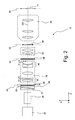
- the FIG. 1 shows in a highly schematic perspective view of a projection exposure apparatus 10, which is suitable for the lithographic production of microstructured components.
- the projection exposure apparatus 10 contains an illumination system 12 for generating a projection light beam, which illuminates a narrow light field 16 on a mask 14 and an annular segment-shaped light field 16 in the exemplary embodiment shown. Structures 18 lying on the mask 14 within the light field 16 are imaged onto a photosensitive layer 22 with the aid of a projection objective 20.
- the photosensitive layer 22, which may be, for example, a photoresist is applied to a wafer 24 or other suitable substrate and is located in the image plane of the projection objective 20. Since the projection objective 20 is generally a magnification ⁇ ⁇ 1, the structures 18 lying within the light field 16 are depicted as being smaller than the area 16 '.
- the mask 14 and the wafer 24 are moved during the projection along a direction designated Y.
- the ratio of the movement speeds is equal to the magnification ⁇ of the projection objective 20. If the projection objective 20 produces an inversion of the image, the movements of the mask 14 and the wafer 22 are in opposite directions, as shown in FIG FIG. 1 is indicated by arrows A1 and A2. In this way, the light field 16 is guided in a scanning movement over the mask 14, so that even larger structured areas can be projected coherently onto the photosensitive layer 22.
- the Y direction is therefore also referred to as scan direction.
- the invention can also be used in the case of projection exposure apparatuses designated as wafer steppers, in which no movement movements take place during the projection.
- the FIG. 2 shows in a simplified and not to scale meridional section details of the illumination system 12.
- the illumination system 12 includes a light source 26, which at least partially generates spatially coherent projection light.
- a light source 26 are lasers, since the light emitted by lasers is spatially and temporally highly coherent.
- the light source 26 is an excimer laser with which light can be generated in the (deep) ultraviolet spectral range.
- the use of short-wave projection light is advantageous because it allows high resolution to be achieved in optical imaging in this way.
- Commonly used are excimer lasers with the laser media KrF, ArF or F 2 , which can be used to generate light with the wavelengths 248 nm, 193 nm and 157 nm, respectively.
- thermal light sources if one removes from the light generated therefrom, e.g. produced by using small apertures, (partially) coherent light beams.
- the light generated by the excimer laser used as the light source 26 is highly concentrated and diverges only slightly. It is therefore first expanded in a beam expander 28.
- the beam expander 28 may, for example, be an adjustable mirror arrangement which increases the dimensions of the approximately rectangular light beam cross section.
- the expanded light beam then passes through an optically birefringent wedge-shaped prism, hereinafter referred to as wedge 32, a compensator element 34 and a diffractive optical element 36.
- wedge 32 an optically birefringent wedge-shaped prism
- compensator element 34 a compensator element 34 and a diffractive optical element 36.
- the diffractive optical element 36 is adjoined by a zoom-axicon module 38, which establishes a Fourier relationship between a field plane 40, in which the diffractive optical element 36 is arranged, and a pupil plane 42.
- a zoom-axicon module 38 which establishes a Fourier relationship between a field plane 40, in which the diffractive optical element 36 is arranged, and a pupil plane 42.
- the zoom axicon assembly 38 includes a zoom lens indicated at 44 and an axicon group 46 which includes two axicon elements with conical and complementary surfaces. With the help of the axicon group 46, the radial light distribution can be changed in order to achieve in this way an annular illumination of the pupil plane 42. By adjusting the zoom lens 44, the diameter of the areas illuminated in the pupil plane 42 can be changed.
- an optical integrator 48 is arranged, which may be, for example, an array of microlens arrays.
- Each microlens forms a secondary one Light source, which generates a divergent light beam with an angle given by the geometry of the microlens angle spectrum.
- the light beams generated by the secondary light sources are superimposed by a condenser 50 in an intermediate field plane 52, whereby it is illuminated very homogeneously.
- a field stop 54 is arranged in the illustrated embodiment, which may comprise a plurality of adjustable cutting edges and / or a plurality of narrow finger-like aperture elements, which are individually inserted into the light path.
- the intermediate field plane 52 is imaged with the aid of a field diaphragm objective 56 onto the object plane 58 of the projection objective 20, in which the mask 14 is arranged.
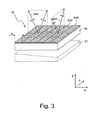
- FIG. 3 shows the diffractive optical element 36 in a perspective view. Underneath, the wedge 32 is indicated by dashed lines in order to illustrate the relative arrangement between the diffractive optical element 36 and the wedge 32.
- the compensator element 34 arranged between them in this exemplary embodiment is not shown for the sake of clarity.
- the diffractive optical element 36 has a substrate 60 which carries at least on one side, here on the side facing away from the wedge 32 side, differently structured regions. In the illustrated embodiment, these areas are periodic Arrangement of strips 62X, 62Y, all of which have the same width w. Each of the strips 62X includes diffractive structures that diffract the light in the X direction, as shown in FIG FIG. 3 for two diffraction orders denoted 64X. The diffraction angles in the ZX plane should be symmetrical with respect to a ZY plane.
- the strips 62Y the same applies to the Y direction, ie they diffract the light exclusively in the YZ plane, which in the FIG. 3 is indicated by two diffraction orders 64Y.
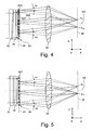
- FIG. 4 shows the wedge 32, the compensator element 34 and the diffractive optical element 36 in a section parallel to the XZ plane.
- the zoom-axicon assembly is indicated here only by a lens 38 ', which produces a Fourier relationship between the field plane 40 and the pupil plane 42.
- all the parallel light rays emanating from the diffractive optical element 36 at the same angle meet at the same point.
- the collimated light passing the stripes 62X diffracts only in the XZ plane by angles + ⁇ x and - ⁇ x , as shown in FIG FIG.
- the rays diffracted by the angle ⁇ x all meet at a point P x in the pupil plane 42 and the rays diffracted by the angle - ⁇ x all converge at a point P -x .
- the pupil plane 42 two points that are the same distance from an optical axis OA of the illumination system 10 and are diametrically opposite each other.
- the strips 62Y which diffract the light exclusively in the YZ plane.
- FIG. 5 which shows the wedge 32, the compensator element 34 and the diffractive optical element 36 in a section parallel to the YZ plane.
- the light rays emanating from the angles ⁇ Y and - ⁇ Y meet at two points P Y and P- Y in the pupil plane 42.
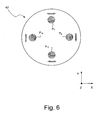
- the light distribution in the pupil plane 42 produced by the diffractive optical element 36 is shown in FIG. It was assumed that the diffraction of the strips 62X, 62Y is determined so as to be formed instead of the points denoted by P X, P X, P Y, and P -Y broader poles.
- the diffraction structures are so small that in the strips 62X, 62Y each region, over the extent of which the change in thickness of the wedge 32 is negligibly small, produces an angular spectrum which in the far field, ie in the pupil plane 42, becomes a pair of poles P X , P -X or P Y , P -Y leads.
- FIG. 7 shows the wedge 32, the compensator element 34 and the diffractive optical element 36 enlarged in a section parallel to the XZ plane.
- falls on the wedge 32 largely collimated, linearly polarized and highly spatially coherent laser light.
- Two rays of the incident on the wedge 32 light beam are in the FIG. 7 denoted 70, 72.
- the linear polarization direction of the laser light within the XY plane is indicated by double arrows 74, the double arrows 74 are thus "folded up" by 90 °.
- the wedge 32 is made of a birefringent material, for example magnesium fluoride.
- the wedge 32 has a wedge angle ⁇ and an optical birefringence axis which makes an angle of 45 ° to the polarization direction 74 of the incident projection light.
- the upper wedge surface 76 which is inclined by the wedge angle .gamma.
- the light rays 70, 72 are broken as they exit the wedge 32 and are thereby deflected in their direction.
- the compensator element 34 has the task of reversing this distraction.
- the compensator element 34 is therefore likewise wedge-shaped, but the wedge angle may differ from the wedge angle ⁇ of the wedge 34, depending on the refractive index of the compensator element 34.
- the polarization state in the XY plane is indicated after the light has passed through the birefringent wedge 32.
- This representation is also (like the double arrows 74) "folded up" by 90 °.
- the polarization state of a light beam after the passage of the wedge 32 depends on how thick the wedge 32 is at the respective passage location of the light beam. Since the thickness of the wedge 32 changes continuously in the X direction, the polarization state along this direction also changes continuously. Thus, as seen in the X-direction, all the states of polarization occur, as in the FIG. 7 are shown below the diffractive optical element 36. It can also be seen from this representation that the change in the polarization state is periodic with the period p.
- the superimposition of the two photons a, b considered here into linearly polarized light can be mathematically determined by the G1.
- E 1 a and E 1 b are the electric field vectors of the two photons a and b and ⁇ describes the phase and thus the polarization state of the field vectors.
- E p 1 a , E s 1 a , E p 1 b and E s 1 b set here equal to 1
- the real components of the electric field vectors E 1 a and E 1 b are parallel or perpendicular to the optical birefringence axis of the wedge 32 designated.
- ⁇ is the wavelength of the light
- ⁇ n is the amount of the difference between the refractive index n 0 of the ordinary ray and the refractive index n a of the extraordinary ray in the birefringent wedge 32 at the wavelength ⁇ .
- the arrangement of stripes 62X, 62Y is chosen to be within a period of width p completely a strip 62X and a strip 62Y has space.
- the two wedges then have the same wedge angle ⁇ / 2.
- the width w of the strips 62X, 62Y can be halved if both birefringent wedges have the wedge angle ⁇ .
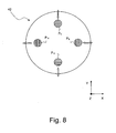
- the diffractive optical element 36 is displaced by half a period p / 2 along the X direction, one obtains in the pupil plane 42 Pole P X , P -X , P Y and P -Y with linearly polarized light in the radial direction, as shown in FIG FIG. 8 is shown.
- FIG. 9 shows in a to the FIG. 3 Similar perspective perspective view of another embodiment of a diffractive optical element, which is here indicated overall with 36 '. Unlike the one in the FIG. 3 In the embodiment shown, the diffractive optical element 32 includes stripes 62 which do not contain diffraction structures. The light passing through the strips 62 therefore remains collimated parallel to the optical axis.
- the non-diffraction patterned stripes 62 are offset by two and a half (generally 2m + 1/2) periods in the illustrated embodiment, light emerging from adjacent unstructured stripes 62 is polarized orthogonal to each other.
- the distance between the unstructured regions 62 is large enough that there is no significant coherence relationship between the photons emerging from the adjacent stripes, an incoherent superposition of orthogonal polarization states in the pupil plane 42 will result, resulting in unpolarized light.
- the light emerging from the strips 62 parallel to the optical axis is focused by the zoom-axicon assembly 38 at a point on the optical axis in the pupil plane 42.
- FIG. 10 shows the resulting pupil plane 42 in one of the FIGS. 6 and 8th ajar representation.
- P c an additional pole, which is designated P c and is penetrated by unpolarized light.
- An alternative way to produce an unpolarized pole is to provide stripes on the diffractive optical element 36, whose width is significantly greater than the spatial coherence cells of the laser light. Then, if the stripe width is exactly a multiple of the period p, then unpolarized light is produced, which is similar to the one already mentioned at the outset US Pat. No. 6,535,273 described finds.
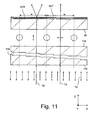
- FIG. 11 shows for another embodiment in one of the FIG. 7 Another way of producing different polarization states is to use a different representation.
- the in the FIG. 11 shown alternative Arrangement comprises a birefringent stepped prism 132, a compensator element 134 and the diffractive optical element 36 of the FIG. 3 ,
- the birefringent prism 132 is designed substantially the same as the wedge 32 in the FIG. 7 shown embodiment.
- the optical birefringence axis also includes an angle of 45 ° to the direction of polarization 74 of the incident projection light.
- the inclined wedge surface 76 which in the in the FIG. 7 however, in the case of the birefringent prism 132, it is replaced by a step surface 176, the steps of which increase along the X direction.
- the birefringent prism 132 thus receives the overall shape of a staircase.
- the compensator element 134 is also formed as a stepped prism, but without being birefringent.
- the compensator element 134 is required only in the event that not only axially parallel rays 70, 72 strike the birefringent prism 132 from below, but also rays which are (slightly) inclined to the optical axis.
- the compensator element 134 then ensures that the directional distribution of the rays passing through the prism 132 and the compensator element 134 remains unchanged.
- the effect of the compensator element 134 corresponds in principle to the effect of the compensator element 34 in FIG FIG. 7 shown Arrangement.
- the compensator element 134 can also have inclined surfaces which are arranged in an inclined manner. In the case of highly paraxial light, the compensator element 134 can be completely eliminated.
- the step surface 176 and thus the distribution of the thickness (dimension along the Z direction) of the birefringent prism 132 along the X direction is set so that incident largely collimated in the Y direction linearly polarized (see "folded" double arrows 74) and highly spatially coherent light is not changed either in its polarization state, the polarization direction is rotated by 90 ° or is converted into right or left circularly polarized light.
- the distribution of the thickness is further set such that each of the strips 62X, 62Y falls light whose polarization state in the X direction changes from circularly polarized to linearly polarized to reverse circularly polarized.
- the pupil plane 42 is linearly polarized along either the Y direction or the X direction.
- each strip 62X, 62Y also be associated with two or more than three different thicknesses.
- each strip 62X, 62Y also be associated with two or more than three different thicknesses.
- thickness tolerances can then compensate each other more easily.
Landscapes
- Physics & Mathematics (AREA)
- General Physics & Mathematics (AREA)
- Optics & Photonics (AREA)
- Exposure And Positioning Against Photoresist Photosensitive Materials (AREA)
- Optical Elements Other Than Lenses (AREA)
- Microscoopes, Condenser (AREA)
- Exposure Of Semiconductors, Excluding Electron Or Ion Beam Exposure (AREA)
- Polarising Elements (AREA)
Abstract
Claims (20)
- Système d'éclairage (12) d'un appareil d'exposition par projection microlithographique (10), comprenant :a) un premier dispositif optique (26, 32 ; 132) pour générer un faisceau lumineux, dans lequel la lumière- possède différents états de polarisation et- est spatialement cohérente au moins partiellement
au moins sur une partie de la section transversale du faisceau lumineux,b) un plan de pupille (42), etc) un deuxième dispositif optique (36, 38),- qui est disposé entre le premier dispositif optique (26, 32 ; 132) et le plan de pupille (42) et- qui répartit le faisceau lumineux sur au moins deux emplacements différents (Px, P-x, Py, P-y) dans le plan de pupille (42) et interfère ce faisant avec les différents états de polarisation générés par le premier dispositif optique pour former des états de polarisation de pupille qui sont différents auxdits au moins deux emplacements (Px, P-x, Py, P-y). - Système d'éclairage selon la revendication 1, dans lequel les états de polarisation du faisceau lumineux généré par le premier dispositif (26, 32 ; 132) changent continuellement et périodiquement au moins sur une partie de la section transversale du faisceau lumineux suivant au moins une direction (X).
- Système d'éclairage selon la revendication 2, dans lequel le premier dispositif présente :a) une source de lumière (26) pour générer une lumière de projection polarisée linéairement et spatialement cohérente au moins partiellement etb) un prisme biréfringent (32 ; 132) qui modifie périodiquement l'état de polarisation d'un faisceau lumineux qui le traverse suivant une direction (X).
- Système d'éclairage selon la revendication 3, dans lequel le prisme (32) est en forme de coin et modifie continuellement l'état de polarisation d'un faisceau lumineux qui le traverse suivant la direction (X).
- Système d'éclairage selon la revendication 3, dans lequel le prisme (132) a un profil d'épaisseur étagé et modifie discontinuellement l'état de polarisation d'un faisceau lumineux qui le traverse suivant la direction (X).
- Système d'éclairage selon une des revendications 3 à 5, dans lequel le prisme (32 ; 132) a un axe optique de biréfringence qui fait un angle de 45° avec une direction de polarisation de la lumière de projection polarisée linéairement.
- Système d'éclairage selon une des revendications précédentes, dans lequel le deuxième dispositif (38) présente un élément optique diffractif (36) qui possède des caractéristiques de diffraction variables localement.
- Système d'éclairage selon la revendication 7, dans lequel l'élément optique diffractif (36) présente au moins deux bandes (62X, 62Y) disposées parallèlement l'une à l'autre qui ont des caractéristiques de diffraction différentes.
- Système d'éclairage selon la revendication 8, dans lequel les caractéristiques de diffraction des bandes (62X, 62Y) alternent périodiquement.
- Système d'éclairage selon la revendication 4 et selon une des revendications 8 ou 9, dans lequel les bandes (62X, 62Y) sont disposées parallèlement à une direction (Y) qui est perpendiculaire à un axe optique (OA) du système d'éclairage (12) et perpendiculaire à une direction suivant laquelle l'épaisseur du prisme (32 ; 132) varie.
- Système d'éclairage selon une des revendications 8 à 10, dans lequel des premières bandes (62X) diffractent la lumière dans plusieurs directions dans un plan X-Z et des deuxièmes bandes (62Y) diffractent la lumière dans plusieurs directions dans un plan Y-Z.
- Système d'éclairage selon la revendication 11, dans lequel les premières bandes (62X) génèrent en champ lointain une distribution dipolaire en direction X et les deuxièmes bandes (62Y) en champ lointain une distribution dipolaire en direction Y.
- Système d'éclairage selon une des revendications 8 à 12, dans lequel la largeur des bandes (62X, 62Y) est choisie de façon que la lumière qui traverse une seule bande (62X, 62Y) ait une direction de polarisation préférentielle en cas de superposition à un desdits au moins deux emplacements (Px, P-x, Py, P-y).
- Système d'éclairage selon la revendication 13, dans lequel la largeur (w) des bandes (62X, 62Y) est égale à la moitié de la période avec laquelle l'état de polarisation du faisceau lumineux qui les traverse change périodiquement.
- Système d'éclairage selon une des revendications 8 à 14, dans lequel la largeur (w) des bandes (62X, 62Y) est choisie de façon que la lumière qui traverse une seule bande (62X, 62Y) soit polarisée au moins essentiellement linéairement en cas de superposition à un desdits au moins deux emplacements (Px, P-x, Py, P-y).
- Système d'éclairage selon une des revendications 8 à 15, dans lequel les bandes (62X, 62Y) ont une largeur (w) qui est assez petite pour que la lumière qui traverse une bande (62X, 62Y) soit spatialement cohérente.
- Système d'éclairage selon une des revendications précédentes, avec un laser excimère comme source de lumière (26).
- Système d'éclairage selon la revendication 16 et selon la revendication 18, dans lequel les bandes (62X, 62Y) ont une largeur (w) inférieure à 0,5 mm.
- Système d'éclairage selon la revendication 18, dans lequel les bandes (62X, 62Y) ont une largeur (w) inférieure à 0,25 mm.
- Procédé de construction de composants microstructurés, présentant les étapes suivantes :a) mise à disposition d'un appareil d'exposition par projection microlithographique (10) équipé d'un système d'éclairage (12) selon une des revendications précédentes ;b) éclairage d'un masque (14) avec le système d'éclairage (12),c) projection du masque éclairé (14) sur une couche photosensible (22).
Applications Claiming Priority (2)
| Application Number | Priority Date | Filing Date | Title |
|---|---|---|---|
| DE102006032878A DE102006032878A1 (de) | 2006-07-15 | 2006-07-15 | Beleuchtungssystem einer mikrolithographischen Projektionsbelichtungsanlage |
| PCT/EP2007/005943 WO2008009353A1 (fr) | 2006-07-15 | 2007-07-05 | Système d'éclairage d'un équipement d'éclairage par projection microlithographique |
Publications (2)
| Publication Number | Publication Date |
|---|---|
| EP2041625A1 EP2041625A1 (fr) | 2009-04-01 |
| EP2041625B1 true EP2041625B1 (fr) | 2012-06-27 |
Family
ID=38536021
Family Applications (1)
| Application Number | Title | Priority Date | Filing Date |
|---|---|---|---|
| EP07765066A Not-in-force EP2041625B1 (fr) | 2006-07-15 | 2007-07-05 | Systeme d'eclairage d'un equipement d'eclairage par projection microlithogafique |
Country Status (5)
| Country | Link |
|---|---|
| US (1) | US20090115991A1 (fr) |
| EP (1) | EP2041625B1 (fr) |
| JP (1) | JP5369319B2 (fr) |
| DE (1) | DE102006032878A1 (fr) |
| WO (1) | WO2008009353A1 (fr) |
Families Citing this family (4)
| Publication number | Priority date | Publication date | Assignee | Title |
|---|---|---|---|---|
| DE102008009601A1 (de) * | 2008-02-15 | 2009-08-20 | Carl Zeiss Smt Ag | Optisches System für eine mikrolithographische Projektionsbelichtungsanlage sowie mikrolithographisches Belichtungsverfahren |
| US9116303B2 (en) * | 2010-03-05 | 2015-08-25 | Canon Kabushiki Kaisha | Hologram with cells to control phase in two polarization directions and exposure apparatus |
| EP2622411B1 (fr) * | 2010-09-28 | 2015-11-04 | Carl Zeiss SMT GmbH | Système optique d'un appareil d'exposition par projection microlithographique et procédé de réduction d'erreurs de disposition d'image |
| DE102011085334A1 (de) * | 2011-10-27 | 2013-05-02 | Carl Zeiss Smt Gmbh | Optisches System in einer Beleuchtungseinrichtung einer mikrolithographischen Projektionsbelichtungsanlage |
Citations (1)
| Publication number | Priority date | Publication date | Assignee | Title |
|---|---|---|---|---|
| US20060055834A1 (en) * | 2002-12-03 | 2006-03-16 | Nikon Corporation | Illumination optical system, exposure apparatus, and exposure method |
Family Cites Families (23)
| Publication number | Priority date | Publication date | Assignee | Title |
|---|---|---|---|---|
| EP0967524A3 (fr) * | 1990-11-15 | 2000-01-05 | Nikon Corporation | Méthode et appareil de projection pour exposition |
| US5459000A (en) * | 1992-10-14 | 1995-10-17 | Canon Kabushiki Kaisha | Image projection method and device manufacturing method using the image projection method |
| JP3985346B2 (ja) * | 1998-06-12 | 2007-10-03 | 株式会社ニコン | 投影露光装置、投影露光装置の調整方法、及び投影露光方法 |
| DE19829612A1 (de) * | 1998-07-02 | 2000-01-05 | Zeiss Carl Fa | Beleuchtungssystem der Mikrolithographie mit Depolarisator |
| US6563567B1 (en) * | 1998-12-17 | 2003-05-13 | Nikon Corporation | Method and apparatus for illuminating a surface using a projection imaging apparatus |
| JP3927753B2 (ja) * | 2000-03-31 | 2007-06-13 | キヤノン株式会社 | 露光装置及びデバイス製造方法 |
| DE10124474A1 (de) * | 2001-05-19 | 2002-11-21 | Zeiss Carl | Mikrolithographisches Belichtungsverfahren sowie Projektionsobjektiv zur Durchführung des Verfahrens |
| JP2003090978A (ja) * | 2001-09-17 | 2003-03-28 | Canon Inc | 照明装置、露光装置及びデバイス製造方法 |
| EP1367446A1 (fr) * | 2002-05-31 | 2003-12-03 | ASML Netherlands B.V. | Appareil lithographique |
| AU2003255441A1 (en) * | 2003-08-14 | 2005-03-29 | Carl Zeiss Smt Ag | Illuminating device for a microlithographic projection illumination system |
| US7408616B2 (en) * | 2003-09-26 | 2008-08-05 | Carl Zeiss Smt Ag | Microlithographic exposure method as well as a projection exposure system for carrying out the method |
| TW201834020A (zh) * | 2003-10-28 | 2018-09-16 | 日商尼康股份有限公司 | 照明光學裝置、曝光裝置、曝光方法以及元件製造方法 |
| WO2005050325A1 (fr) * | 2003-11-05 | 2005-06-02 | Carl Zeiss Smt Ag | Systeme d'eclairage optimisant la polarisation |
| TWI512335B (zh) * | 2003-11-20 | 2015-12-11 | 尼康股份有限公司 | 光束變換元件、光學照明裝置、曝光裝置、以及曝光方法 |
| JP4497968B2 (ja) * | 2004-03-18 | 2010-07-07 | キヤノン株式会社 | 照明装置、露光装置及びデバイス製造方法 |
| US7324280B2 (en) * | 2004-05-25 | 2008-01-29 | Asml Holding N.V. | Apparatus for providing a pattern of polarization |
| JP2006005319A (ja) | 2004-06-21 | 2006-01-05 | Canon Inc | 照明光学系及び方法、露光装置及びデバイス製造方法 |
| US7548370B2 (en) * | 2004-06-29 | 2009-06-16 | Asml Holding N.V. | Layered structure for a tile wave plate assembly |
| JP2006196715A (ja) * | 2005-01-13 | 2006-07-27 | Nikon Corp | 光束変換素子、照明光学装置、露光装置、および露光方法 |
| JP2006269462A (ja) * | 2005-03-22 | 2006-10-05 | Sony Corp | 露光装置および照明装置 |
| US7317512B2 (en) * | 2005-07-11 | 2008-01-08 | Asml Netherlands B.V. | Different polarization in cross-section of a radiation beam in a lithographic apparatus and device manufacturing method |
| US20070058151A1 (en) * | 2005-09-13 | 2007-03-15 | Asml Netherlands B.V. | Optical element for use in lithography apparatus and method of conditioning radiation beam |
| US7525642B2 (en) * | 2006-02-23 | 2009-04-28 | Asml Netherlands B.V. | Lithographic apparatus and device manufacturing method |
-
2006
- 2006-07-15 DE DE102006032878A patent/DE102006032878A1/de not_active Withdrawn
-
2007
- 2007-07-05 EP EP07765066A patent/EP2041625B1/fr not_active Not-in-force
- 2007-07-05 JP JP2009518757A patent/JP5369319B2/ja not_active Expired - Fee Related
- 2007-07-05 WO PCT/EP2007/005943 patent/WO2008009353A1/fr active Application Filing
-
2008
- 2008-11-17 US US12/272,297 patent/US20090115991A1/en not_active Abandoned
Patent Citations (1)
| Publication number | Priority date | Publication date | Assignee | Title |
|---|---|---|---|---|
| US20060055834A1 (en) * | 2002-12-03 | 2006-03-16 | Nikon Corporation | Illumination optical system, exposure apparatus, and exposure method |
Also Published As
| Publication number | Publication date |
|---|---|
| WO2008009353A1 (fr) | 2008-01-24 |
| DE102006032878A1 (de) | 2008-01-17 |
| JP2009544146A (ja) | 2009-12-10 |
| US20090115991A1 (en) | 2009-05-07 |
| EP2041625A1 (fr) | 2009-04-01 |
| JP5369319B2 (ja) | 2013-12-18 |
Similar Documents
| Publication | Publication Date | Title |
|---|---|---|
| WO2005017620A2 (fr) | Dispositif d'eclairage et polariseur destines a un systeme d'exposition de projection microlithographique | |
| WO2006021540A2 (fr) | Systeme optique, precisement objectif ou dispositif d'eclairage d'une installation d'exposition par projection microlithographique | |
| WO2005085955A2 (fr) | Dispositif de filtre de transmission | |
| WO2005059653A2 (fr) | Dispositif de temporisation ayant un effet optique de polarisation et dispositif d'eclairage de projection microlithographique comportant un tel dispositif de temporisation | |
| DE102006032810A1 (de) | Beleuchtungsoptik für eine Mikrolithografie-Projektionsbelichtungsanlage, Beleuchtungssystem mit einer derartigen Beleuchtungsoptik, mikrolithografie-Projektionsbelichtungsanlage mit einem derartigen Beleuchtungssystem, mikrolithografisches Herstellungsverfahren für Bauelemente sowie mit diesem Verfahren hergestelltes Bauelement | |
| DE10123725A1 (de) | Projektionsbelichtungsanlage der Mikrolithographie, Optisches System und Herstellverfahren | |
| DE10010131A1 (de) | Mikrolithographie - Projektionsbelichtung mit tangentialer Polarisartion | |
| DE10124474A1 (de) | Mikrolithographisches Belichtungsverfahren sowie Projektionsobjektiv zur Durchführung des Verfahrens | |
| DE10344010A1 (de) | Wabenkondensor und Beleuchtungssystem damit | |
| DE102010029339A1 (de) | Optisches System für eine mikrolithographische Projektionsbelichtungsanlage sowie mikrolithographisches Belichtungsverfahren | |
| DE102007042047A1 (de) | Teilsystem einer Beleuchtungseinrichtung einer mikrolithographischen Projektionsbelichtungsanlage | |
| DE102007010650A1 (de) | Beleuchtungseinrichtung einer mikrolithographischen Projektionsbelichtungsanlage | |
| EP1721219A2 (fr) | Systeme d'eclairage pour installation d'exposition par projection microlithographique | |
| WO2003067334A2 (fr) | Systeme d'eclairage a polarisation optimisee | |
| EP2041625B1 (fr) | Systeme d'eclairage d'un equipement d'eclairage par projection microlithogafique | |
| DE102013202590A1 (de) | EUV-Lichtquelle zur Erzeugung eines Nutz-Ausgabestrahls für eine Projektionsbelichtungsanlage | |
| WO2006131517A2 (fr) | Dispositif d'eclairage pour un systeme d'eclairage par projection pour la microlithographie | |
| EP1754111A1 (fr) | Systeme d'eclairage d'un dispositif d'eclairage par projection micro-lithographique | |
| DE102011082481A1 (de) | Beleuchtungssystem einer mikrolithographischen projektionsbelichtungsanlage und verfahren zu deren betrieb | |
| WO2004102273A2 (fr) | Systeme d'eclairage pourvu d'un module axicon | |
| DE102005031084A1 (de) | Mikrolithografisches Belichtungsverfahren sowie Projektionsbelichtungsanlage zur Durchführung des Verfahrens | |
| DE102012205045A1 (de) | Optisches System einer mikrolithographischen Projektionsbelichtungsanlage | |
| WO2007066225A2 (fr) | Systeme d'eclairage par projection pour la microlithographie et procede de fabrication de composes microstructures | |
| DE102007019831A1 (de) | Beleuchtungseinrichtung einer mikrolithographischen Projektionsbelichtungsanlage | |
| DE102011085334A1 (de) | Optisches System in einer Beleuchtungseinrichtung einer mikrolithographischen Projektionsbelichtungsanlage |
Legal Events
| Date | Code | Title | Description |
|---|---|---|---|
| PUAI | Public reference made under article 153(3) epc to a published international application that has entered the european phase |
Free format text: ORIGINAL CODE: 0009012 |
|
| 17P | Request for examination filed |
Effective date: 20080322 |
|
| AK | Designated contracting states |
Kind code of ref document: A1 Designated state(s): AT BE BG CH CY CZ DE DK EE ES FI FR GB GR HU IE IS IT LI LT LU LV MC MT NL PL PT RO SE SI SK TR |
|
| AX | Request for extension of the european patent |
Extension state: AL BA HR MK RS |
|
| DAX | Request for extension of the european patent (deleted) | ||
| RBV | Designated contracting states (corrected) |
Designated state(s): DE FR NL |
|
| RAP1 | Party data changed (applicant data changed or rights of an application transferred) |
Owner name: CARL ZEISS SMT GMBH |
|
| 17Q | First examination report despatched |
Effective date: 20110706 |
|
| RIC1 | Information provided on ipc code assigned before grant |
Ipc: G02B 27/28 20060101ALI20111130BHEP Ipc: G02B 27/42 20060101ALI20111130BHEP Ipc: G03F 7/20 20060101AFI20111130BHEP |
|
| GRAP | Despatch of communication of intention to grant a patent |
Free format text: ORIGINAL CODE: EPIDOSNIGR1 |
|
| GRAS | Grant fee paid |
Free format text: ORIGINAL CODE: EPIDOSNIGR3 |
|
| GRAA | (expected) grant |
Free format text: ORIGINAL CODE: 0009210 |
|
| AK | Designated contracting states |
Kind code of ref document: B1 Designated state(s): DE FR NL |
|
| REG | Reference to a national code |
Ref country code: DE Ref legal event code: R096 Ref document number: 502007010127 Country of ref document: DE Effective date: 20120823 |
|
| REG | Reference to a national code |
Ref country code: NL Ref legal event code: T3 |
|
| REG | Reference to a national code |
Ref country code: FR Ref legal event code: ST Effective date: 20130329 |
|
| PG25 | Lapsed in a contracting state [announced via postgrant information from national office to epo] |
Ref country code: FR Free format text: LAPSE BECAUSE OF NON-PAYMENT OF DUE FEES Effective date: 20120827 |
|
| PLBE | No opposition filed within time limit |
Free format text: ORIGINAL CODE: 0009261 |
|
| STAA | Information on the status of an ep patent application or granted ep patent |
Free format text: STATUS: NO OPPOSITION FILED WITHIN TIME LIMIT |
|
| 26N | No opposition filed |
Effective date: 20130328 |
|
| REG | Reference to a national code |
Ref country code: DE Ref legal event code: R097 Ref document number: 502007010127 Country of ref document: DE Effective date: 20130328 |
|
| PGFP | Annual fee paid to national office [announced via postgrant information from national office to epo] |
Ref country code: NL Payment date: 20190719 Year of fee payment: 13 |
|
| PGFP | Annual fee paid to national office [announced via postgrant information from national office to epo] |
Ref country code: DE Payment date: 20190719 Year of fee payment: 13 |
|
| REG | Reference to a national code |
Ref country code: DE Ref legal event code: R119 Ref document number: 502007010127 Country of ref document: DE |
|
| REG | Reference to a national code |
Ref country code: NL Ref legal event code: MM Effective date: 20200801 |
|
| PG25 | Lapsed in a contracting state [announced via postgrant information from national office to epo] |
Ref country code: NL Free format text: LAPSE BECAUSE OF NON-PAYMENT OF DUE FEES Effective date: 20200801 |
|
| PG25 | Lapsed in a contracting state [announced via postgrant information from national office to epo] |
Ref country code: DE Free format text: LAPSE BECAUSE OF NON-PAYMENT OF DUE FEES Effective date: 20210202 |