-
The present invention relates to a wideband antenna and a manufacturing method for the same, and more particularly to a multi-mode resonant wideband antenna and a manufacturing method for the same.
-
The application of antenna in wireless LAN card is not only limited by the character of the antenna, but also by the space and the cost of the wireless LAN card. The chip antenna is usually applied in the wireless LAN card because of its small size. However, the chip antenna has the deficiencies of the high cost and the narrow bandwidth. Further, while the chip antenna is used in the wireless LAN card, the real bandwidth thereof is often narrower than expected because of the interference from the printed circuit board (PCB) layout.
-
If there is enough space in the wireless LAN card, the printed antenna is usually applied firstly. The printed antennas include the monopole antenna, the dipole antenna, the planar inverted-F antenna, and the ring antenna, characterized in that the planar inverted-F antenna is frequently used because it could efficiently reduce the size occupied by the printed antenna on PCB. Nevertheless, the bandwidth of the planar inverted-F antenna is always limited by the special structure itself. If the bandwidth of an antenna is not broad enough, the most electromagnetic wave delivered by the antenna would easily be reflected back by the surrounding objects that are close to the antenna. Further, the character of the return loss of the antenna is possible to be affected, which makes the deviation of the central frequency. For overcoming these deficiencies, an antenna that could provide a broader bandwidth and a better performance in return loss, and could overcome the affection of the surrounding objects to the return loss and the central frequency deviation, without any additional cost, is needed.
-
In order to overcome the drawbacks in the prior art, a multi-mode resonant wideband antenna and a manufacturing method for the same are provided. The particular design in the present invention not only solves the problems described above, but also is easy to be implemented. Thus, the invention has the utility for the industry.
-
In accordance with the present invention, there is provided a wireless transmit/receive unit for transmitting and receiving an electromagnetic wave. The wireless transmit/receive unit includes a radiating element (11) and a feeding line (12). The radiating element (11) is a metal piece having a first edge (113) with a first length, a second edge (114) with a second length, and a plurality of cutouts (111a-111e). The first edge (113) and the second edge (114) are separated from each other and the first length is longer than the second length. Further, the cutouts (111a-111e) are formed on the metal piece and make the metal piece have a zigzag shape. In addition, the feeding line (12) is electrically connected to the second edge (114).
-
Preferably, the metal piece is an inverted triangle-shaped metal plate or an inverted trapezium-shaped metal plate, and the metal piece has an effective electrical length that is a multiple of a half wavelength of the electromagnetic wave.
-
Preferably, the first length is a multiple of a quarter wavelength of the electromagnetic wave and the cutouts (111a-111e) being cutting slots have a total length that is a multiple of a half wavelength of the electromagnetic wave.
-
Preferably, each of the cutouts (111 a-111e) being cutting slots has a width of 20 milliinches.
-
Preferably, the wireless transmit/receive unit further includes a reference ground surface (14) coupled to a dielectric substrate (13), and the feeding line (12) is mounted on the dielectric substrate (13) made of an FR4 laminate.
-
Preferably, the wireless transmit/receive unit is configured in a wireless transmission device.
-
Preferably, the radiating element (11) is a meander line (112) having a first terminal (115) and a second terminal (116). The meander line (112) includes a first section (112e), a second section (112d), a third section (112a), a first bending part (117), and a second bending part (118). The first section (112e) has a first length and is connected to the first terminal (115), and the second section (112d) has a second length and is connected to the first section (112e) via the first bending part (117). The third section (112a) has a third length and is connected at one end to the second section (112d) via the second bend part (118) and is connected at another end to the second terminal (116). Further, the first length is shorter than the second length, and the second length is shorter than the third length. The feeding line (12) is electrically connected to the first terminal (115).
-
Preferably, the third length is a multiple of a quarter wavelength of the electromagnetic wave and the meander line (112) has a total length that is a multiple of a half wavelength of the electromagnetic wave.
-
In accordance with another aspect of the invention, there is provided a method for increasing a bandwidth of an antenna. The method includes steps as follows. The first step is to provide a radiating element (11) that has a first edge (113) with a first length and a second edge (114) with a second length, where the first length is longer than the second length. The second step is to form a plurality of cutouts (111a-111e) on the radiating element (11) for producing a plurality of horizontal electric fields parallel to the cutouts (111a-111e) and a plurality of perpendicular electric fields perpendicular to the cutouts (111a-111e), where the horizontal electric fields offset with each other and the perpendicular electric fields superimpose with each other.
-
Preferably, the cutouts (111a-111e) are formed by one of a cutting process and an etching process.
-
The above objects and advantages of the present invention will become more readily apparent to those ordinarily skilled in the art after reviewing the following detailed descriptions and accompanying drawings, in which:
-
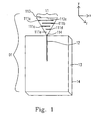
Fig. 1 is an illustrating diagram showing a multi-mode resonant wideband antenna according to the first preferred embodiment of the present invention;
-
Fig. 2 is an illustrating diagram showing a radiating element according to the second preferred embodiment of the present invention;
-
Fig. 3A is a polar graph showing an horizontal field pattern of the multi-mode resonant wideband antenna in the XZ plane according to the first preferred embodiment of the present invention;
-
Fig. 3B is a polar graph showing an perpendicular field pattern of the multi-mode resonant wideband antenna in the XZ plane according to the first preferred embodiment of the present invention;
-
Fig. 4A is a polar graph showing an horizontal field pattern of the multi-mode resonant wideband antenna in the XY plane according to the first preferred embodiment of the present invention;
-
Fig. 4B is a polar graph showing an perpendicular field pattern of the multi-mode resonant wideband antenna in the XY plane according to the first preferred embodiment of the present invention; and
-
Fig. 5 is a diagram showing the return loss of the multi-mode resonant wideband antenna in different frequencies according to the first preferred embodiment of the present invention.
-
The present invention will now be described more specifically with reference to the following embodiments. It is to be noted that the following descriptions of preferred embodiments of this invention are presented herein for the purposes of illustration and description only; it is not intended to be exhaustive or to be limited to the precise form disclosed.
-
Please refer to Fig. 1, which is an illustrating diagram showing a multi-mode resonant wideband antenna according to the first preferred embodiment of the present invention. The multi-mode resonant wideband antenna 01 of the present invention includes a radiating element 11, a feeding line 12, a dielectric substrate 13, and a reference ground surface 14. The radiating element 11 is formed from a metal piece having a shape of inverted triangle, and the metal piece has a first edge 113, a second edge 114, plural sections 112a-112e (of which only 112a is marked in Fig. 1) and plural cutouts 111a-111e. The number of cutouts could vary based on necessary in practice, as well as five cutouts 111a-111e exist in our embodiment. The respective cutouts 111a-111e have successively decreasing lengths, which makes the radiating element 11 have a zigzag shape. Further, the dielectric substrate 13 is a FR4 substrate.
-
In order to receive/transmit electromagnetic waves having different wavelengths, the length of the edges of the radiating element 11 and each of the cutouts 111a-111e could be adjusted accordingly. In our first preferred embodiment, the first edge 113 has a length equal to a quarter wavelength of the electromagnetic wave having a frequency of 2.45GHz, and the respective cutouts 111a-111e have a width of 20 milliinches, which is easy to be carried out by the present technology. Further, the sum of the length of the respective sections 112a-112e is equal to a half wavelength of the electromagnetic wave having a frequency of 2.45GHz.
-
Please refer to Fig. 2, which is an illustrating diagram of a radiating element according to the second preferred embodiment of the present invention. The radiating element 11 includes a meander line 112 connected to the feeding line 12, and plural cutouts 111a-111e (of which only cutting slot 111a is marked in Fig. 2). The meander line 112 further includes a first terminal 115, a second terminal 116, plural sections 112a-112e (of which only 112a, 112d and 112e are shown in Fig. 2), and plural bending parts 117-121. As showed in Fig. 2, as providing a current to the first terminal 115 via the feeding line 12, the current would be transmitted from the first terminal 115 to the second terminal 116 via the meander line 112, which not only makes the respective sections 112a-112e have an individual horizontal electric field (-x/+x) but also makes each bending part 117-121 have a perpendicular electric field (+y). The horizontal electric fields of the respective sections 112a-112e would offset each other because of the alternatively opposite directions (-x/+x) thereof, and the perpendicular electric fields of each bending part 117-121 would superimpose each other because of the same direction (+y) thereof. In addition, as the total length of the meander line 112 (which is also the sum of the length of the respective sections 112a-112e and the individual bending parts 117-121) is equal to a half wavelength of the received electromagnetic wave, there would be a highest resonant current existing in the bending part 120, which makes the bending part 120 be the main site where the antenna radiates or receives the electromagnetic wave. It is noted that the section numbers could be modified according to the need in practice. Please refer to Figs. 3A and 3B, which are polar graphs showing a horizontal and a perpendicular field patterns of the multi-mode resonant wideband antenna in the XZ plane according to the first preferred embodiment of the present invention. As the Fig. 3B shows, the sum of the electric fields in the perpendicular direction (+y) make the invented antenna being an omnidirectional antenna in XZ plane.
-
Please refer to Figs. 4A and 4B, which are polar graphs showing a horizontal and a perpendicular field patterns of the multi-mode resonant wideband antenna in the XY plane according to the first preferred embodiment of the present invention. Because the cutouts 111a-111e have very narrow widths (20 milliinches), the respective sections 112a-112e have relatively broad widths, which decreases the impedance of the radiating element 11 and improves the invented antenna performance. As the Fig. 4A shows, the antenna of the present invention has an ideal performance of 3 dBi peak gain in the XY plane.
-
Further, since the cutouts 111a-111e have very narrow widths (20 milliinches), the multiple leakage currents would be induced easily across each cutouts 111a-111e, which makes the radiating element 11 have multiple effective electrical lengths from a quarter to a half wavelength of the received electromagnetic wave. Therefore, by coupling multiple effective electrical lengths, a broader bandwidth could be easily provided.
-
Please refer to Fig. 5, which is a diagram showing the return loss of the multi-mode resonant wideband antenna according to the first preferred embodiment of the present invention. The y-axis presents the return loss, and the x-axis presents the operating frequencies. As described above, the radiating element 11 has an effective electrical length equal to a half wavelength of the received electromagnetic wave, which makes the radiating element 11 have a high perpendicular current in the bending part 120. A corresponding resonant frequency of 2.4 GHz could be found in Fig. 5, which is labeled as mark 1. Further, the bending part 120 is far away form the reference ground surface 14, which could decrease the interference induced by the ground 14. In addition, an effective electrical length equal to a quarter wavelength of the received electromagnetic wave would make the radiating element 11 have a high perpendicular current in the bending part 117. A corresponding resonant frequency of 2.5 GHz that is labeled as mark 3 could also be found in Fig. 5. Besides, the triangle-shaped radiating element 11 has the benefit of decreasing the coupling effect existing between the radiating element 11 and the reference ground surface 14. As the Fig. 5 shows, in an operational definition of -20 dB, the bandwidth of the invented antenna is 200 MHz. However, in an operational definition of -10 dB, the bandwidth of the invented antenna is 600 MHz.
-
While the invention has been described in terms of what is presently considered to be the most practical and preferred embodiments, it is to be understood that the invention needs not be limited to the disclosed embodiments. On the contrary, it is intended to cover various modifications and similar arrangements included within the spirit and scope of the appended claims which are to be accorded with the broadest interpretation so as to encompass all such modifications and similar structures.