EP2040248A2 - Pixel driving method and apparatus for organic light emitting device - Google Patents
Pixel driving method and apparatus for organic light emitting device Download PDFInfo
- Publication number
- EP2040248A2 EP2040248A2 EP07124161A EP07124161A EP2040248A2 EP 2040248 A2 EP2040248 A2 EP 2040248A2 EP 07124161 A EP07124161 A EP 07124161A EP 07124161 A EP07124161 A EP 07124161A EP 2040248 A2 EP2040248 A2 EP 2040248A2
- Authority
- EP
- European Patent Office
- Prior art keywords
- power supply
- light emitting
- voltage
- organic light
- supply voltage
- Prior art date
- Legal status (The legal status is an assumption and is not a legal conclusion. Google has not performed a legal analysis and makes no representation as to the accuracy of the status listed.)
- Ceased
Links
Images




Classifications
-
- G—PHYSICS
- G09—EDUCATION; CRYPTOGRAPHY; DISPLAY; ADVERTISING; SEALS
- G09G—ARRANGEMENTS OR CIRCUITS FOR CONTROL OF INDICATING DEVICES USING STATIC MEANS TO PRESENT VARIABLE INFORMATION
- G09G3/00—Control arrangements or circuits, of interest only in connection with visual indicators other than cathode-ray tubes
- G09G3/20—Control arrangements or circuits, of interest only in connection with visual indicators other than cathode-ray tubes for presentation of an assembly of a number of characters, e.g. a page, by composing the assembly by combination of individual elements arranged in a matrix no fixed position being assigned to or needed to be assigned to the individual characters or partial characters
- G09G3/22—Control arrangements or circuits, of interest only in connection with visual indicators other than cathode-ray tubes for presentation of an assembly of a number of characters, e.g. a page, by composing the assembly by combination of individual elements arranged in a matrix no fixed position being assigned to or needed to be assigned to the individual characters or partial characters using controlled light sources
- G09G3/30—Control arrangements or circuits, of interest only in connection with visual indicators other than cathode-ray tubes for presentation of an assembly of a number of characters, e.g. a page, by composing the assembly by combination of individual elements arranged in a matrix no fixed position being assigned to or needed to be assigned to the individual characters or partial characters using controlled light sources using electroluminescent panels
- G09G3/32—Control arrangements or circuits, of interest only in connection with visual indicators other than cathode-ray tubes for presentation of an assembly of a number of characters, e.g. a page, by composing the assembly by combination of individual elements arranged in a matrix no fixed position being assigned to or needed to be assigned to the individual characters or partial characters using controlled light sources using electroluminescent panels semiconductive, e.g. using light-emitting diodes [LED]
- G09G3/3208—Control arrangements or circuits, of interest only in connection with visual indicators other than cathode-ray tubes for presentation of an assembly of a number of characters, e.g. a page, by composing the assembly by combination of individual elements arranged in a matrix no fixed position being assigned to or needed to be assigned to the individual characters or partial characters using controlled light sources using electroluminescent panels semiconductive, e.g. using light-emitting diodes [LED] organic, e.g. using organic light-emitting diodes [OLED]
- G09G3/3225—Control arrangements or circuits, of interest only in connection with visual indicators other than cathode-ray tubes for presentation of an assembly of a number of characters, e.g. a page, by composing the assembly by combination of individual elements arranged in a matrix no fixed position being assigned to or needed to be assigned to the individual characters or partial characters using controlled light sources using electroluminescent panels semiconductive, e.g. using light-emitting diodes [LED] organic, e.g. using organic light-emitting diodes [OLED] using an active matrix
- G09G3/3233—Control arrangements or circuits, of interest only in connection with visual indicators other than cathode-ray tubes for presentation of an assembly of a number of characters, e.g. a page, by composing the assembly by combination of individual elements arranged in a matrix no fixed position being assigned to or needed to be assigned to the individual characters or partial characters using controlled light sources using electroluminescent panels semiconductive, e.g. using light-emitting diodes [LED] organic, e.g. using organic light-emitting diodes [OLED] using an active matrix with pixel circuitry controlling the current through the light-emitting element
-
- G—PHYSICS
- G09—EDUCATION; CRYPTOGRAPHY; DISPLAY; ADVERTISING; SEALS
- G09G—ARRANGEMENTS OR CIRCUITS FOR CONTROL OF INDICATING DEVICES USING STATIC MEANS TO PRESENT VARIABLE INFORMATION
- G09G2300/00—Aspects of the constitution of display devices
- G09G2300/08—Active matrix structure, i.e. with use of active elements, inclusive of non-linear two terminal elements, in the pixels together with light emitting or modulating elements
- G09G2300/0809—Several active elements per pixel in active matrix panels
- G09G2300/0842—Several active elements per pixel in active matrix panels forming a memory circuit, e.g. a dynamic memory with one capacitor
-
- G—PHYSICS
- G09—EDUCATION; CRYPTOGRAPHY; DISPLAY; ADVERTISING; SEALS
- G09G—ARRANGEMENTS OR CIRCUITS FOR CONTROL OF INDICATING DEVICES USING STATIC MEANS TO PRESENT VARIABLE INFORMATION
- G09G2300/00—Aspects of the constitution of display devices
- G09G2300/08—Active matrix structure, i.e. with use of active elements, inclusive of non-linear two terminal elements, in the pixels together with light emitting or modulating elements
- G09G2300/0809—Several active elements per pixel in active matrix panels
- G09G2300/0842—Several active elements per pixel in active matrix panels forming a memory circuit, e.g. a dynamic memory with one capacitor
- G09G2300/0861—Several active elements per pixel in active matrix panels forming a memory circuit, e.g. a dynamic memory with one capacitor with additional control of the display period without amending the charge stored in a pixel memory, e.g. by means of additional select electrodes
-
- G—PHYSICS
- G09—EDUCATION; CRYPTOGRAPHY; DISPLAY; ADVERTISING; SEALS
- G09G—ARRANGEMENTS OR CIRCUITS FOR CONTROL OF INDICATING DEVICES USING STATIC MEANS TO PRESENT VARIABLE INFORMATION
- G09G2300/00—Aspects of the constitution of display devices
- G09G2300/08—Active matrix structure, i.e. with use of active elements, inclusive of non-linear two terminal elements, in the pixels together with light emitting or modulating elements
- G09G2300/0809—Several active elements per pixel in active matrix panels
- G09G2300/0842—Several active elements per pixel in active matrix panels forming a memory circuit, e.g. a dynamic memory with one capacitor
- G09G2300/0861—Several active elements per pixel in active matrix panels forming a memory circuit, e.g. a dynamic memory with one capacitor with additional control of the display period without amending the charge stored in a pixel memory, e.g. by means of additional select electrodes
- G09G2300/0866—Several active elements per pixel in active matrix panels forming a memory circuit, e.g. a dynamic memory with one capacitor with additional control of the display period without amending the charge stored in a pixel memory, e.g. by means of additional select electrodes by means of changes in the pixel supply voltage
-
- G—PHYSICS
- G09—EDUCATION; CRYPTOGRAPHY; DISPLAY; ADVERTISING; SEALS
- G09G—ARRANGEMENTS OR CIRCUITS FOR CONTROL OF INDICATING DEVICES USING STATIC MEANS TO PRESENT VARIABLE INFORMATION
- G09G2310/00—Command of the display device
- G09G2310/02—Addressing, scanning or driving the display screen or processing steps related thereto
- G09G2310/0202—Addressing of scan or signal lines
- G09G2310/0218—Addressing of scan or signal lines with collection of electrodes in groups for n-dimensional addressing
-
- G—PHYSICS
- G09—EDUCATION; CRYPTOGRAPHY; DISPLAY; ADVERTISING; SEALS
- G09G—ARRANGEMENTS OR CIRCUITS FOR CONTROL OF INDICATING DEVICES USING STATIC MEANS TO PRESENT VARIABLE INFORMATION
- G09G2320/00—Control of display operating conditions
- G09G2320/02—Improving the quality of display appearance
- G09G2320/0223—Compensation for problems related to R-C delay and attenuation in electrodes of matrix panels, e.g. in gate electrodes or on-substrate video signal electrodes
-
- G—PHYSICS
- G09—EDUCATION; CRYPTOGRAPHY; DISPLAY; ADVERTISING; SEALS
- G09G—ARRANGEMENTS OR CIRCUITS FOR CONTROL OF INDICATING DEVICES USING STATIC MEANS TO PRESENT VARIABLE INFORMATION
- G09G2320/00—Control of display operating conditions
- G09G2320/02—Improving the quality of display appearance
- G09G2320/0247—Flicker reduction other than flicker reduction circuits used for single beam cathode-ray tubes
Definitions
- the present disclosure relates to a method for driving a panel for an organic light emitting device (OLED), and more particularly, to a pixel driving method and apparatus for an OLED capable of preventing a non-uniform brightness due to different levels of a common voltage at each position inside a panel, and capable of preventing a flicker phenomenon due to a short data voltage emission period at a large panel.
- OLED organic light emitting device
- an organic light emitting device is one of plane-type light emitting devices.
- an organic light emitting layer is disposed between two electrodes facing each other, and when a voltage is applied between the two electrodes, electrons injected from one electrode are combined with holes injected from another electrode at the organic light emitting layer. By the coupling, molecules on the light emitting layer are excited to be in a ground level, and thereby light is emitted.
- the OLED is being spotlighted as the next generation display apparatus owing to an excellent viewing characteristic, a light weight, a thin thickness, and a low voltage driving.
- the OLED is classified into an Active-Matrix type OLED and a Passive-Matrix type OLED according to whether a switching device provided at a unit pixel of a panel exists.
- FIG. 1A is a block diagram showing an OLED in accordance with the conventional art.
- the conventional OLED comprises a scan driving unit 10 for sequentially outputting scan signals to drive scan lines (S1 ⁇ Sn) on a display panel 30 under control of a signal controller (not shown); a data driving unit 20 for outputting data voltages to data lines (D1 ⁇ Dm) on the display panel 30; and a display panel 30 having a plurality of pixels (PXs) at intersections between the scan lines (S1 ⁇ Sn) and the data lines (D1 ⁇ Dm).
- a scan driving unit 10 for sequentially outputting scan signals to drive scan lines (S1 ⁇ Sn) on a display panel 30 under control of a signal controller (not shown); a data driving unit 20 for outputting data voltages to data lines (D1 ⁇ Dm) on the display panel 30; and a display panel 30 having a plurality of pixels (PXs) at intersections between the scan lines (S1 ⁇ Sn) and the data lines (D1 ⁇ Dm).
- the pixels of the active-matrix type OLED are classified into voltage writing pixels, current writing pixels, and digital driving pixels according to a driving method.
- FIG. 1 B is a circuit for driving pixels (PXs) on the display panel 30 of FIG. 1A .
- the pixel circuit includes a switching transistor (T11) transmitting data voltages (Data) supplied through the data lines (D) to a storage capacitor (C11) by being driven by the scan signals supplied through the scan lines(S); a storage capacitor (C11) charging the data voltage (Data) by being connected between a gate terminal of a driving transistor (T12) and a lower power supply voltage terminal(Vss); a driving transistor (T12) for supplying a driving current corresponding to the data voltage (Data) charged to the storage capacitor (C11) to an organic light emitting diode (OLED11); and an OLED 11 emitting light having a brightness corresponding to the driving current by having an anode connected to an upper power supply voltage terminal (ELVDD) and having a cathode connected to a drain of the driving transistor (T12)
- the transistors T11 and T12 are implemented as N-channel type thin film transistors (TFTs).
- FIG. 1B is an exemplary view showing one of a plurality of pixels (including a driving circuit) connected to an optional scan line.
- the switching transistor (T11) is turned ON by a corresponding scan signal among the scan signals (Scan [1] ⁇ Scan [N]). And, the data voltage (Data) supplied from the data driving unit 20 through a corresponding data line among the data lines (D1 ⁇ Dm) is charged to the storage capacitor (C11) through the switching transistor (T11), and is maintained for a data voltage emission period.
- the driving transistor (T12) is turned ON by the data voltage (Data) charged to the storage capacitor (C11), and a certain amount of driving current corresponding to the data voltage (Data) flows through the organic light emitting diode (OLED 11). Accordingly, the OLED 11 emits light with the corresponding brightness.
- I OLED 1 2 ⁇ W L ⁇ C SINx ⁇ V DATA - Vss - V TH 2
- the "L” denotes a channel length of the driving transistor (T12)
- the “W” denotes a channel width of the driving transistor (T12)
- the “C SINx” is a capacitor component of a gate insulator
- the “V TH” denotes a threshold voltage
- the “V DATA” is a data voltage charged to the storage capacitor (C11).
- FIG. 3 is a schematic view showing an array structure of each power supply voltage supply line on the display panel 30.
- a lower power supply voltage (Vss) supply line 32 is arrayed on an array portion 31 with a mesh structure so as to minimize a resistance.
- Vss lower power supply voltage
- other lower power supply voltage supply lines 33 and 34 having a wider width are arrayed, thereby smoothly supplying the lower power supply voltage (Vss).
- an upper power supply voltage (ELVDD) of a certain level i.e., 15V is continuously supplied to the anode of the OLED 11 for one frame period.
- the driving current (I OLED ) of the OLED 11, and the resistance (R line )of the lower power supply voltage supply line 32 have different values according to each position inside the display panel 30.
- the conventional organic light emitting device has the following problems. At the time of programming the data voltages, the potential on the lower power supply voltage supply line 32 is increased due to the organic light emitting diode (OLED) of each pixel, the lower power supply voltage supply line 32 having a mesh structure, and the current flowing therethrough. Accordingly, the driving voltage of the driving transistor inside the pixel is lowered, thereby lowering a brightness of the organic light emitting diode.
- OLED organic light emitting diode
- an object of the present disclosure is to provide a pixel driving method and apparatus for an organic light emitting device, capable of preventing a driving voltage of a driving transistor inside a pixel from dropping by charging a data voltage to a storage capacitor, in a state that supply of a power supply voltage to an organic light emitting diode (OLED) is cut-off, and then by starting to supply the power supply voltage to the OLED.
- OLED organic light emitting diode
- Another object of the present disclosure is to provide a pixel driving method and apparatus for an organic light emitting device, capable of sufficiently obtaining a data voltage programming period and a lighting duration of an organic light emitting diode regardless of a size of a display panel.
- a pixel driving method for an organic light emitting device comprising: in a data voltage programming period, charging a data voltage supplied through a data line to a storage capacitor, by cutting off supply of a power supply voltage to an organic light emitting diode (OLED) and by driving a switching transistor; and in a data voltage emission period, supplying the power supply voltage to the OLED, and making the OLED emit light by the data voltage charged to the storage capacitor.
- OLED organic light emitting diode
- a pixel driving method for an organic light emitting device comprising: defining a display panel of the organic light emitting device into a plurality of display panel regions in a horizontal direction such that a plurality of adjacent scan lines can be included; making pixels inside the plurality of display panel regions share one lower power supply voltage among a plurality of lower power supply voltages supplied by being diverged; and determining a data voltage programming period and a data voltage emission period in one frame period according to each of the display panel regions.
- a pixel driving apparatus for an organic light emitting device comprising a display panel, wherein the display panel defines a plurality of display panel regions in a horizontal direction such that a plurality of adjacent scan lines can be included; makes pixels inside the plurality of display panel regions share one lower power supply voltage among a plurality of lower power supply voltages supplied by being diverged; and determines a data voltage programming period and a data voltage emission period in one frame period according to each of the display panel regions.
- FIG. 4A is a view of a pixel circuit to which a pixel driving method according to the present invention is applied, which is implemented as an N-channel thin film transistor (TFT).
- TFT thin film transistor
- the pixel circuit includes a switching transistor (T41) driven by scan signals, for transmitting data voltages (Data) supplied through data lines to a storage capacitor C41, in a state that supply of an upper power supply voltage (ELVDD) is cut-off; a storage capacitor (C41)connected between a gate terminal of a driving transistor (T42) and a lower power supply voltage terminal (Vss), for charging the data voltage (Data), in a state that supply of the upper power supply voltage (ELVDD) is cut-off; a driving transistor (T42) for supplying a driving current corresponding to the data voltage (Data) charged to the storage capacitor (C41) to an organic light emitting diode (OLED 41), in a state that the upper power supply voltage (ELVDD) is supplied; and an organic light emitting diode (OLED 41) having an anode connected to the upper power supply voltage (ELVDD) and a cathode connected to a drain of the driving transistor (T42), for emitting light
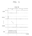
- the ELVDD of a 'high' level is not supplied to the anode of the OLED 41 during all of one frame period. Rather, the ELVDD of a 'low' level (OV) is supplied during the data voltage programming period (P1) of said one frame period.
- FIG. 4A is an exemplary view showing one of a plurality of pixels (including a driving circuit) arrayed on an optional horizontal line.
- the data voltage (data) supplied trough the corresponding data line is charged to the storage capacitor (C41) through the switching transistor (T41), and is maintained for a data voltage emission period (P2).
- the data voltage (Data) of a 'high' level charged to the storage capacitor (C41) is supplied to the gate terminal of the driving transistor (T42), thereby turning on the driving transistor (T42).
- ELVDD upper power supply voltage
- Vds drain and source terminals
- a voltage of a lower power supply voltage node (A) is maintained as the original level (0V) regardless of a resistance of the lower power supply voltage supply line 32.
- the data voltage (Data) having a desired level can be charged to the storage capacitor (C41).
- the ELVDD of a 'high' level is supplied to the anode of the OLED 41.
- the driving transistor (T42) Since the gate terminal of the driving transistor (T42) is being supplied with the data voltage (Data) stored at the storage capacitor (C41), the driving transistor (T42) is turned-ON.
- the OLED 41 emits light.
- the gate node (B) is in an electrical floating status. Therefore, when the voltage (Vss) of the lower power supply voltage node (A) is increased to the Vss', the voltage of the gate node (B)is also increased by a coupling with the storage capacitor (C41).
- V B Data . N + Vss ⁇ - Vss
- a voltage (Vgs) between the gate and source terminals of the driving transistor (T42) does not change.
- the driving current (I OLED ) of the OLED 41 is not influenced by the voltage change of the lower power supply voltage node (A), but is influenced by the data voltage stored in the storage capacitor (C41).
- the driving current (I OLED )of the OLED 41 is expressed as the following equation 5.
- the following table shows each change of the voltages of the nodes (A) and (B), and the driving current (I OLED ) of the OLED 41 in the data voltage programming period (P1) and the data voltage emission period (P2). Operation Period 1 Period 2 Node 'A' Vss Vss' (potential rising) Node 'B' Data. [ N ] Data. [ N ]+ Vss'-Vss I OLED 0 k ( Data [ N ]- Vss-V TH ) 2
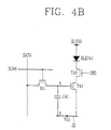
- FIG. 4B shows a method for cutting-off supply of the ELVDD by using a switching transistor.
- a drain and a source of the switching transistor (T43) are respectively connected between the cathode of the OLED 41 and the drain of the driving transistor (T42). And, the switching transistor (T43) is turned-OFF as a switching control signal (EMS) of a 'low' level is outputted to the gate of the switching transistor (T43) by a signal controller (not shown) in the data voltage programming period (P1).
- EMS switching control signal
- FIG. 6A is a view of a pixel circuit to which the pixel driving method according to the present is applied, which shows a P-channel type Thin Film Transistor (TFT).
- TFT Thin Film Transistor
- the P-channel type TFT includes a switching transistor (T61) driven by a scan signal, for transmitting a data voltage(Data) supplied through a data line to a storage capacitor (C61), in a state that supply of a lower power supply voltage (Vss) is cut-off; a storage capacitor (C61) connected between a gate terminal of a driving transistor (T62) and an upper power supply voltage terminal(ELVDD), for charging the data voltage (Data) in a state that supply of the lower power supply voltage (Vss) is cut-off; a driving transistor (T62) for supplying a driving current corresponding to the data voltage (Data) charged to the storage capacitor (C61) to an organic light emitting diode (OLED61), in a state that the lower power supply voltage (Vss) is supplied; and an OLED 61 having an anode connected to a source terminal of the driving transistor (T62) and having a cathode connected to the lower power supply voltage (Vss), for emitting light having
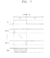
- Vss The lower power supply voltage (Vss) of a 'low' level is not supplied to the cathode of the OLED 61 during all of one frame period. Rather, the Vss of a 'high' level is supplied during the data voltage programming period (P1) of said one frame period.
- FIG. 6A is an exemplary view showing one of a plurality of pixels (including a driving circuit) arrayed on an optional horizontal line.
- the data voltage (data) supplied trough the corresponding data line is charged to the storage capacitor (C61) through the switching transistor (T61), and is maintained for the data voltage emission period (P2).
- the data voltage (Data) of a 'low' level charged to the storage capacitor (C61) is supplied to the gate terminal of the driving transistor (T62), thereby turning on the driving transistor (T62).
- Vss lower power supply voltage
- Vds drain and source terminals
- the current does not flow to the OLED 61 through the upper power supply voltage (ELVDD) supply line. That is, the driving current (I OLED )of the OLED 61 becomes '0'.
- a voltage of an upper power supply voltage node (A) is maintained as the original level (15V) during the data voltage programming period (P1) regardless of a resistance of the upper power supply voltage (ELVDD) supply line.
- the data voltage (Data) having a desired level can be charged to the storage capacitor (C61).
- the low power supply voltage (Vss) of a 'low' level (OV) is supplied to the cathode of the OLED 61.
- the driving transistor (T62) Since the gate terminal of the driving transistor (T62) is being supplied with the data voltage (Data) stored at the storage capacitor (C61), the driving transistor (T62) is turned-ON.
- the OLED 61 since the upper power supply voltage (ELVDD) is supplied to the OLED 61 and the driving transistor (T62), the OLED 61 emits light.
- ELVDD upper power supply voltage
- VDD voltage of the upper power supply voltage node (A)
- VDD' the Ohm' law
- Vss lower power supply voltage
- Vgs voltage between the gate and source terminals of the driving transistor (T62) does not change. Accordingly, the driving current (I OLED )of the OLED 61 is not influenced by the voltage change of the upper power supply voltage node (A), but is influenced by the data voltage stored in the storage capacitor (C61).
- the driving current (I OLED )of the OLED 61 is expressed as the following equation 7.
- FIG. 6B shows a method for cutting-off supply of the ELVDD by using a switching transistor in the same manner as FIG. 4B .
- a drain and a source of the switching transistor (T63) are respectively connected between the anode of the OLED 61 and the drain of the driving transistor (T62). And, the switching transistor (T63) is turned-OFF as a switching control signal (EMS) of a 'high' level is outputted to the gate of the switching transistor (T63) by a signal controller (not shown) in the data voltage programming period (P1).
- EMS switching control signal
- FIG. 8 is a view of an anode contact type-pixel circuit in which the driving transistor comes in contact with the anode of the organic light emitting diode, which shows an N-channel TFT in the same manner as FIG. 6A .
- the pixel circuit includes a switching transistor (T81) driven by a scan signal, for transmitting a data voltage (Data) supplied through a data line to a storage capacitor C81, in a state that supply of an upper power supply voltage (ELVDD) is cut-off; a storage capacitor (C81)connected between a gate terminal and a source terminal of a driving transistor (T82), for charging the data voltage (Data), in a state that supply of the upper power supply voltage (ELVDD) is cut-off; a driving transistor (T82) for supplying a driving current corresponding to the data voltage (Data) charged to the storage capacitor (C81) to an organic light emitting diode (OLED 81), in a state that supply of the upper power supply voltage (ELVDD) is cut-off; and an organic light emitting diode (OLED 81) having an anode connected to the source terminal of the driving transistor (T82) and a cathode connected to a lower power supply voltage terminal (Vss
- the ELVDD of a 'high' level is not supplied to the drain of the driving transistor (T82) during all of one frame period. Rather, the ELVDD of a 'low' level is supplied during the data voltage programming period (P1) of said one frame period.
- FIG. 8 is an exemplary view showing one of a plurality of pixels (including a driving circuit) arrayed on an optional horizontal line.
- the data voltage (data) supplied trough the corresponding data line is charged to the storage capacitor (C81) through the switching transistor (T81), and is maintained for the data voltage emission period (P2).
- the data voltage (Data) of a 'high' level charged to the storage capacitor (C81) is supplied to the gate terminal_of the driving transistor (T82), thereby turning on the driving transistor (T82).
- the upper power supply voltage (ELVDD) to the drain of the driving transistor (T82) is cut-off, a voltage between the drain and source terminals (Vds) becomes 'OV'.
- the current does not flow to the lower power supply voltage (Vss) supply line 32 through the OLED 81 and the driving transistor (T82). That is, the driving current (I OLED ) of the OLED 81 becomes '0'.
- the data voltage (Data) having a desired level can be charged to the storage capacitor (C81).
- the ELVDD of a 'high' level is supplied to the driving transistor (T82) in the data voltage emission period (P2).
- the driving transistor (T82) Since the gate terminal of the driving transistor (T82) is being supplied with the data voltage (Data) stored at the storage capacitor (C81), the driving transistor (T82) is turned-ON.
- the OLED 81 emits light.
- the gate node (B) is in an electrical floating status. Therefore, when the voltage (Vss) of the anode node (A) is increased to the V OLED , the voltage of the gate node (B)is also increased by a coupling with the storage capacitor (C81).
- V B Data . N + V OLED - V SS
- the voltage of the gate node (B) also changes, a voltage (Vgs) between the gate and source terminals of the driving transistor (T82) does not change.
- the driving current (I OLED ) of the OLED 81 is not influenced by the voltage change of the anode node (A), but is influenced by the data voltage stored in the storage capacitor (C81).
- the data voltage programming period (P1) in one frame period is set, during which the data voltage is charged to the storage capacitor in a state that supply of the power supply voltage to the organic light emitting diode (OLED) is cut-off. Accordingly, a driving voltage of the driving transistor is prevented from dropping.
- time corresponding to the other period except the data voltage programming period (P1) in one frame period is determined as the data voltage emission period (P2), that is, a lighting duration of the OLED, an entire lighting duration of the organic light emitting diode is reduced.
- the lighting duration of the organic light emitting diode can be obtained without being influenced by the data voltage programming period (P1)
- the data voltage programming period (P1) becomes relatively longer. Accordingly, there is a difficulty in sufficiently obtaining the lighting duration of the organic light emitting diode, and thus a brightness flicker phenomenon occurs.
- the data voltage programming period and the lighting duration of the organic light emitting diode are sufficiently obtained regardless of the size of the display panel.
- FIG. 9 is an exemplary view of a display panel of an organic light emitting device (OLED) according to the present invention.
- the display panel 30 is defined as a plurality of display panel regions (30A ⁇ 30K) in a horizontal direction so that a plurality of adjacent scan lines can be included. Then, pixels inside the plurality of display panel regions (30A ⁇ 30K) share one lower power supply voltage among a plurality of lower power supply voltages (Vss[1] ⁇ Vss[K]) supplied from the lower power supply voltage supply terminals (Vss_supply) by being diverged. And, a data voltage programming period and a data voltage emission period are determined in one frame period according to each of the display panel regions (30A ⁇ 30K).
- Scan lines (S1 ⁇ Sn) and data lines (D1 ⁇ Dm) are arrayed on the display panel 30 in the same manner as a general display panel.
- the display panel 30 is defined as a plurality of display panel regions (30A ⁇ 30K) in a horizontal direction so that a plurality of adjacent scan lines can be included. Then, a plurality of lower power supply voltages (Vss[1] ⁇ Vss[K]) are supplied to the display panel regions (30A ⁇ 30K), respectively.
- a large display panel 30 having 760 scan lines is defined as 10 display panel regions (30A ⁇ 30K).
- each of the ten display panel regions (30A ⁇ 30K) is implemented to include 76 scan lines [(S1 ⁇ S76),(S77 ⁇ S152) ⁇ (S685 ⁇ S760)].
- the display panel 30 of the present invention has to be provided with 768 scan lines (S1 ⁇ Sn) since it is implemented as an XGA-type (1024 ⁇ 768).
- the display panel 30 is supposed to have 760 scan lines for convenience.
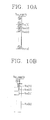
- FIGS. 10A and 10B show examples for distributing the lower power supply voltages (Vss[1] ⁇ Vss[k]).
- the lower power supply voltages (Vss) is supplied to 9 sub-lines among the 10 sub-lines, and a data voltage emission operation is performed at the other one sub-line by a switching control signal (EMS) in a state that supply of the lower power supply voltage (Vss) is cut-off.
- EMS switching control signal
- FIG. 10A is an exemplary view showing a method for obtaining lower power supply voltages (Vss[1] ⁇ Vss[k]) by sequentially diverging a power supplied to the lower power supply voltage supply terminal (Vss_supply) from an external power supply unit (not shown), and then for supplying the obtained lower power supply voltages (Vss[1] ⁇ Vss[k]) to each of the display panel regions (30A ⁇ 30K).
- Vss[1] ⁇ Vss[k] due to distribution resistance values, voltages are diverged from distribution nodes (S1 ⁇ Sk)in the order of "Vss[1]>Vss[2]> ⁇ Vss[k-1]>Vss[k]".
- the previously diverged voltage is higher than the next one by a small degree.
- a voltage of a common node is expressed as a lower power supply voltage rising (Vss rising) by current applied to the diverged 9 lines.
- Vss rising maintains a nearly constant value even if it may be varied little by little by an image change.
- FIG. 10B is an exemplary view showing a method for obtaining lower power supply voltages (Vss[1] ⁇ Vss[k]) by diverging a power supplied to the lower power supply voltage supply terminal (Vss_supply) from an external power supply unit (not shown) at the same position, and then for supplying the obtained lower power supply voltages (Vss[1] ⁇ Vss[k]) to each of the display panel regions (30A ⁇ 30K).
- each of the lower power supply voltages (Vss[1] ⁇ Vss[k]) has the same level as the common node (SO).
- the lower power supply voltages (Vss[1] ⁇ Vss[k]) are respectively supplied to the corresponding lower power supply voltage supply lines in the display panel regions (30A ⁇ 30K) by being diverged as shown in FIG. 10B .
- the lower power supply voltage (Vss1) is diverged into 76 lower power supply voltages in the same manner as FIG. 10B , and is supplied to the corresponding lower power supply voltage supply line.
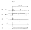
- FIGS. 11A to 11E are timing diagrams showing a data voltage programming period (P1), a data voltage emission period (P2), scan signals, and data voltages on the display panel regions (30A ⁇ 30K) to which the lower power supply voltages (Vss[1] ⁇ Vss[k]) are respectively supplied.
- FIGS. 11A and 11B show examples of the data voltage programming period (P1) and the data voltage emission period (P2) with respect to each of the display panel regions (30A ⁇ 30K).
- the display panel 30 is defined as 10 display panel regions (30A ⁇ 30K)
- 1/10 of one frame period is set as the data voltage programming period (P1) with respect to each of the display panel regions (30A ⁇ 30K)
- the rest 9/10of the one frame period is set as the data voltage emission period (P2).
- FIGS. 11C and 11D are timing diagrams showing scan signals with respect to each of the display panel regions (30A ⁇ 30K), which are same as general timing diagrams.
- FIG. 11E is a timing diagram showing data voltages supplied through data lines (D1 ⁇ Dn) with respect to each of the display panel regions (30A ⁇ 30K), which are same as a general timing diagram.
- the data voltage programming period (P1) is set with respect to the first display panel region (30A) including all the pixels (PXs) connected to first to 76 th scan lines (G1 ⁇ G76).
- the 76 scan signals (Scan[1] ⁇ Scan[76]) are sequentially supplied to the first to 76 th scan lines (G1 ⁇ G76) in the data voltage programming period (P1), thereby turning-ON the switching transistors (T41) connected to the scan signals inside all the pixels (PXs).
- data voltages (DATA) are supplied to the switching transistors (T41) through the data lines (D1 ⁇ Dm).
- the data voltage (DATA) is charged to each storage capacitor (C41) through the switching transistors (T41) inside the respective pixels (PXs), and is maintained for the data voltage emission period (P2).
- the data voltage programming and emission operations for the other display panel regions (30B ⁇ 30K) are performed in the same manner as the display panel region 30A.
- the data voltage programming period and the lighting duration of the organic light emitting diode can be sufficiently obtained regardless of the size of the display panel 30.
- a data voltage of a desired level can be precisely charged by charging the data voltage to the storage capacitor in a state that supply of the power supply voltage supplied to the organic light emitting diode (OLED) is cut-off. Also, in the data voltage emission period, the power supply to the OLED is started, thereby preventing a driving voltage of the driving transistor from changing. Accordingly, a non-uniform brightness of the OLED is solved.
Landscapes
- Engineering & Computer Science (AREA)
- Physics & Mathematics (AREA)
- Computer Hardware Design (AREA)
- General Physics & Mathematics (AREA)
- Theoretical Computer Science (AREA)
- Control Of El Displays (AREA)
- Control Of Indicators Other Than Cathode Ray Tubes (AREA)
- Electroluminescent Light Sources (AREA)
Abstract
Description
- The present disclosure relates to subject matter contained in priority Korean Application No.
10-2007-096141, filed on September 20, 2007 - The present disclosure relates to a method for driving a panel for an organic light emitting device (OLED), and more particularly, to a pixel driving method and apparatus for an OLED capable of preventing a non-uniform brightness due to different levels of a common voltage at each position inside a panel, and capable of preventing a flicker phenomenon due to a short data voltage emission period at a large panel.
- Generally, an organic light emitting device (OLED)is one of plane-type light emitting devices. According to the OLED, an organic light emitting layer is disposed between two electrodes facing each other, and when a voltage is applied between the two electrodes, electrons injected from one electrode are combined with holes injected from another electrode at the organic light emitting layer. By the coupling, molecules on the light emitting layer are excited to be in a ground level, and thereby light is emitted. The OLED is being spotlighted as the next generation display apparatus owing to an excellent viewing characteristic, a light weight, a thin thickness, and a low voltage driving.
- The OLED is classified into an Active-Matrix type OLED and a Passive-Matrix type OLED according to whether a switching device provided at a unit pixel of a panel exists.
-
FIG. 1A is a block diagram showing an OLED in accordance with the conventional art. - As shown, the conventional OLED comprises a
scan driving unit 10 for sequentially outputting scan signals to drive scan lines (S1∼Sn) on adisplay panel 30 under control of a signal controller (not shown); adata driving unit 20 for outputting data voltages to data lines (D1∼Dm) on thedisplay panel 30; and adisplay panel 30 having a plurality of pixels (PXs) at intersections between the scan lines (S1∼Sn) and the data lines (D1∼Dm). - The pixels of the active-matrix type OLED are classified into voltage writing pixels, current writing pixels, and digital driving pixels according to a driving method.
-
FIG. 1 B is a circuit for driving pixels (PXs) on thedisplay panel 30 ofFIG. 1A . - As shown, the pixel circuit includes a switching transistor (T11) transmitting data voltages (Data) supplied through the data lines (D) to a storage capacitor (C11) by being driven by the scan signals supplied through the scan lines(S); a storage capacitor (C11) charging the data voltage (Data) by being connected between a gate terminal of a driving transistor (T12) and a lower power supply voltage terminal(Vss); a driving transistor (T12) for supplying a driving current corresponding to the data voltage (Data) charged to the storage capacitor (C11) to an organic light emitting diode (OLED11); and an OLED 11 emitting light having a brightness corresponding to the driving current by having an anode connected to an upper power supply voltage terminal (ELVDD) and having a cathode connected to a drain of the driving transistor (T12) Here, the transistors T11 and T12 are implemented as N-channel type thin film transistors (TFTs).
- The operation of the conventional circuit for driving pixels will be explained with reference to
FIGS. 2 and3 . - In each frame period, positive scan signals (Scan [1]∼ Scan [N]) are sequentially supplied from the
scan driving unit 10 to the scan lines (S1∼Sn) on thedisplay panel 30, thereby driving the pixels (PXs) on a corresponding scan line (horizontal line).FIG. 1B is an exemplary view showing one of a plurality of pixels (including a driving circuit) connected to an optional scan line. - The switching transistor (T11) is turned ON by a corresponding scan signal among the scan signals (Scan [1]∼ Scan [N]). And, the data voltage (Data) supplied from the
data driving unit 20 through a corresponding data line among the data lines (D1∼Dm) is charged to the storage capacitor (C11) through the switching transistor (T11), and is maintained for a data voltage emission period. - The driving transistor (T12) is turned ON by the data voltage (Data) charged to the storage capacitor (C11), and a certain amount of driving current corresponding to the data voltage (Data) flows through the organic light emitting diode (OLED 11). Accordingly, the OLED 11 emits light with the corresponding brightness.
- Here, the driving current (IOLED) flowing on the OLED 11 is expressed as the following
equation 1.
- Here, the "L" denotes a channel length of the driving transistor (T12), the "W" denotes a channel width of the driving transistor (T12), the "CSINx" is a capacitor component of a gate insulator, the "VTH" denotes a threshold voltage, and the "VDATA" is a data voltage charged to the storage capacitor (C11).
-
FIG. 3 is a schematic view showing an array structure of each power supply voltage supply line on thedisplay panel 30. - As shown, a lower power supply voltage (Vss)
supply line 32 is arrayed on anarray portion 31 with a mesh structure so as to minimize a resistance. On each outer periphery of thearray portion 31 and thedisplay panel 30, other lower power supplyvoltage supply lines 33 and 34 having a wider width are arrayed, thereby smoothly supplying the lower power supply voltage (Vss). - As shown in
FIG. 2 , an upper power supply voltage (ELVDD) of a certain level (i.e., 15V) is continuously supplied to the anode of the OLED 11 for one frame period. - In a data voltage programming period, when data voltages are charged to the storage capacitors (C11) of the pixels (PXs) inside the
display panel 30, about1µA of current flows through the OLED 11 and the driving transistor (T12). The current flows to the lower power supplyvoltage supply lines 33 and 34 through the lower power supplyvoltage supply line 32. Accordingly, the current flowing in thedisplay panel 30 has a total amount corresponding to several∼several tens of mA, and thus a potential on the lower power supplyvoltage supply line 32 is increased. The increased lower power supply voltage (Vss') is expressed as the followingequation 2.
- Here, the driving current (IOLED) of the OLED 11, and the resistance (Rline)of the lower power supply
voltage supply line 32 have different values according to each position inside thedisplay panel 30. - As the potential on the lower power supply
voltage supply line 32 is increased, a driving voltage of the driving transistor (T12) inside the pixel is lowered, thereby lowering a brightness of the OLED 11. As the lower power supply voltage (Vss) changes to the Vss', the driving current (IOLED) of the OLED 11 is lowered, which is expressed as the followingequation 3.
- The conventional organic light emitting device has the following problems. At the time of programming the data voltages, the potential on the lower power supply
voltage supply line 32 is increased due to the organic light emitting diode (OLED) of each pixel, the lower power supplyvoltage supply line 32 having a mesh structure, and the current flowing therethrough. Accordingly, the driving voltage of the driving transistor inside the pixel is lowered, thereby lowering a brightness of the organic light emitting diode. - Furthermore, since the brightness is lowered at the respective pixels by different levels, a non-uniform brightness is entirely caused.
- Therefore, an object of the present disclosure is to provide a pixel driving method and apparatus for an organic light emitting device, capable of preventing a driving voltage of a driving transistor inside a pixel from dropping by charging a data voltage to a storage capacitor, in a state that supply of a power supply voltage to an organic light emitting diode (OLED) is cut-off, and then by starting to supply the power supply voltage to the OLED.
- Another object of the present disclosure is to provide a pixel driving method and apparatus for an organic light emitting device, capable of sufficiently obtaining a data voltage programming period and a lighting duration of an organic light emitting diode regardless of a size of a display panel.
- To achieve these and other advantages and in accordance with the purpose of the present disclosure, as embodied and broadly described herein, there is provided a pixel driving method for an organic light emitting device, comprising: in a data voltage programming period, charging a data voltage supplied through a data line to a storage capacitor, by cutting off supply of a power supply voltage to an organic light emitting diode (OLED) and by driving a switching transistor; and in a data voltage emission period, supplying the power supply voltage to the OLED, and making the OLED emit light by the data voltage charged to the storage capacitor.
- According to another aspect of the present invention, there is provided a pixel driving method for an organic light emitting device, comprising: defining a display panel of the organic light emitting device into a plurality of display panel regions in a horizontal direction such that a plurality of adjacent scan lines can be included; making pixels inside the plurality of display panel regions share one lower power supply voltage among a plurality of lower power supply voltages supplied by being diverged; and determining a data voltage programming period and a data voltage emission period in one frame period according to each of the display panel regions.
- To achieve these and other advantages and in accordance with the purpose of the present disclosure, as embodied and broadly described herein, there is also provided a pixel driving apparatus for an organic light emitting device, comprising a display panel, wherein the display panel defines a plurality of display panel regions in a horizontal direction such that a plurality of adjacent scan lines can be included; makes pixels inside the plurality of display panel regions share one lower power supply voltage among a plurality of lower power supply voltages supplied by being diverged; and determines a data voltage programming period and a data voltage emission period in one frame period according to each of the display panel regions.
- The foregoing and other objects, features, aspects and advantages of the present disclosure will become more apparent from the following detailed description of the present disclosure when taken in conjunction with the accompanying drawings.
- The accompanying drawings, which are included to provide a further understanding of the invention and are incorporated in and constitute a part of this specification, illustrate embodiments of the invention and together with the description serve to explain the principles of the invention.
-
-
FIG. 1A is a block diagram showing an organic light emitting device (OLED) in accordance with the conventional art; -
FIG. 1 B is a pixel circuit in accordance with the conventional art; -
FIG. 2 is a waveform ofFIGS. 1A and 1B ; -
FIG. 3 is a schematic view showing an arrangement structure of power supply voltage supply lines on a display panel; -
FIG. 4A is a view of a pixel circuit to which a pixel driving method according to the present invention is applied; -
FIG. 4B is a view of another pixel circuit to which the pixel driving method according to the present invention is applied; -
FIG. 5 is a waveform showing the pixel circuit ofFIG. 4A ; -
FIG. 6A is a view of still another pixel circuit to which the pixel driving method according to the present is applied; -
FIG. 6B is a view of yet still another pixel circuit to which the pixel driving method according to the present is applied; -
FIG. 7 is a waveform showing the pixel circuit ofFIG. 6A ; -
FIG. 8 is a view of further yet still another pixel circuit to which the pixel driving method according to the present is applied; -
FIG. 9 is an exemplary view of a display panel of an organic light emitting device (OLED) according to the present invention; -
FIGS. 10A and 10B are exemplary views showing each lower power supply voltage; and -
FIGS.11A to 11E are timing diagrams showing a display panel driving according to the present invention. - Reference will now be made in detail to the preferred embodiments of the present disclosure, examples of which are illustrated in the accompanying drawings.
-
FIG. 4A is a view of a pixel circuit to which a pixel driving method according to the present invention is applied, which is implemented as an N-channel thin film transistor (TFT). - As shown, the pixel circuit according to the present invention includes a switching transistor (T41) driven by scan signals, for transmitting data voltages (Data) supplied through data lines to a storage capacitor C41, in a state that supply of an upper power supply voltage (ELVDD) is cut-off; a storage capacitor (C41)connected between a gate terminal of a driving transistor (T42) and a lower power supply voltage terminal (Vss), for charging the data voltage (Data), in a state that supply of the upper power supply voltage (ELVDD) is cut-off; a driving transistor (T42) for supplying a driving current corresponding to the data voltage (Data) charged to the storage capacitor (C41) to an organic light emitting diode (OLED 41), in a state that the upper power supply voltage (ELVDD) is supplied; and an organic light emitting diode (OLED 41) having an anode connected to the upper power supply voltage (ELVDD) and a cathode connected to a drain of the driving transistor (T42), for emitting light with a brightness corresponding to the driving current.
- Hereinafter, a pixel driving method on the pixel circuit will be explained in more detail with reference to
FIG. 5 . - The ELVDD of a 'high' level is not supplied to the anode of the OLED 41 during all of one frame period. Rather, the ELVDD of a 'low' level (OV) is supplied during the data voltage programming period (P1) of said one frame period.
- In this state, positive scan signals (Scan[1]∼Scan[N])are sequentially supplied to the respective horizontal lines, thereby driving the pixels on the horizontal lines.
-
FIG. 4A is an exemplary view showing one of a plurality of pixels (including a driving circuit) arrayed on an optional horizontal line. - Here, the data voltage (data) supplied trough the corresponding data line is charged to the storage capacitor (C41) through the switching transistor (T41), and is maintained for a data voltage emission period (P2).
- The data voltage (Data) of a 'high' level charged to the storage capacitor (C41) is supplied to the gate terminal of the driving transistor (T42), thereby turning on the driving transistor (T42). However, since supply of the upper power supply voltage (ELVDD) to the anode of the OLED 41 is cut-off, a voltage between drain and source terminals (Vds) becomes 'OV'.
- Accordingly, a current does not flow to the lower power supply voltage (Vss)
supply line 32 through the OLED 41 and the driving transistor (T42). That is, the driving current (IOLED) of the OLED 41 becomes '0'. - Since the current does not flow to the lower power supply
voltage supply line 32 through the OLED 41, a voltage of a lower power supply voltage node (A) is maintained as the original level (0V) regardless of a resistance of the lower power supplyvoltage supply line 32. - Accordingly, the data voltage (Data) having a desired level can be charged to the storage capacitor (C41).
- Next, when the data voltage programming operation (scanning operation) is completed, the switching transistor (T41) is turned-off and thereby a gate node (B) is in an electrical floating status.
- Next, in the data voltage emission period (P2), the ELVDD of a 'high' level is supplied to the anode of the OLED 41.
- Since the gate terminal of the driving transistor (T42) is being supplied with the data voltage (Data) stored at the storage capacitor (C41), the driving transistor (T42) is turned-ON.
- Here, since the current flows to the lower power supply
voltage supply line 32 through the OLED 41 and the driving transistor (T42), the OLED 41 emits light. - As all the pixels on the
display panel 30 are operated, a large amount of current flows to the lower power supplyvoltage supply line 32. Accordingly, the voltage (Vss) of the lower power supply voltage node (A) is increased to Vss' according to the Ohm' law (V=IR). - Here, since the switching transistor (T41) is turned-OFF, the gate node (B) is in an electrical floating status. Therefore, when the voltage (Vss) of the lower power supply voltage node (A) is increased to the Vss', the voltage of the gate node (B)is also increased by a coupling with the storage capacitor (C41).
- The voltage (VB)of the gate node (B) is expressed as the following equation 4.

- A current flows to the lower power supply voltage node (A) through the OLED 41 and the driving transistor (T42) by the supplied ELVDD in the data voltage emission period (P2), and thus the voltage of the lower power supply voltage node (A) changes from the Vss to the Vss'. However, since the voltage of the gate node (B) also changes, a voltage (Vgs) between the gate and source terminals of the driving transistor (T42) does not change.
- Accordingly, the driving current (IOLED) of the OLED 41 is not influenced by the voltage change of the lower power supply voltage node (A), but is influenced by the data voltage stored in the storage capacitor (C41).
- The driving current (IOLED)of the OLED 41 is expressed as the following equation 5.

- The following table shows each change of the voltages of the nodes (A) and (B), and the driving current (IOLED) of the OLED 41 in the data voltage programming period (P1) and the data voltage emission period (P2).
Operation Period 1 Period 2Node 'A' Vss Vss' (potential rising) Node 'B' Data.[N] Data.[N]+Vss'-Vss I OLED 0 k (Data[N]-Vss-VTH) 2 - In the data voltage programming period (P1) of one frame period, so as to prevent a current from flowing to the lower power supply voltage (Vss)
supply line 32 through the OLED 41 and the driving transistor (T42), supply of the ELVDD may be cut-off by various methods. -
FIG. 4B shows a method for cutting-off supply of the ELVDD by using a switching transistor. - More concretely, a drain and a source of the switching transistor (T43) are respectively connected between the cathode of the OLED 41 and the drain of the driving transistor (T42). And, the switching transistor (T43) is turned-OFF as a switching control signal (EMS) of a 'low' level is outputted to the gate of the switching transistor (T43) by a signal controller (not shown) in the data voltage programming period (P1).
-
FIG. 6A is a view of a pixel circuit to which the pixel driving method according to the present is applied, which shows a P-channel type Thin Film Transistor (TFT). - As shown, the P-channel type TFT includes a switching transistor (T61) driven by a scan signal, for transmitting a data voltage(Data) supplied through a data line to a storage capacitor (C61), in a state that supply of a lower power supply voltage (Vss) is cut-off; a storage capacitor (C61) connected between a gate terminal of a driving transistor (T62) and an upper power supply voltage terminal(ELVDD), for charging the data voltage (Data) in a state that supply of the lower power supply voltage (Vss) is cut-off; a driving transistor (T62) for supplying a driving current corresponding to the data voltage (Data) charged to the storage capacitor (C61) to an organic light emitting diode (OLED61), in a state that the lower power supply voltage (Vss) is supplied; and an OLED 61 having an anode connected to a source terminal of the driving transistor (T62) and having a cathode connected to the lower power supply voltage (Vss), for emitting light having a brightness corresponding to the driving current.
- Hereinafter, a pixel driving method on the pixel circuit will be explained in more detail with reference to
FIG. 7 . - The lower power supply voltage (Vss) of a 'low' level is not supplied to the cathode of the OLED 61 during all of one frame period. Rather, the Vss of a 'high' level is supplied during the data voltage programming period (P1) of said one frame period.
- In this state, negative scan signals (Scan[1]∼Scan[N])are sequentially supplied to the respective horizontal lines, thereby driving the pixels on the horizontal lines.
FIG. 6A is an exemplary view showing one of a plurality of pixels (including a driving circuit) arrayed on an optional horizontal line. - Here, the data voltage (data) supplied trough the corresponding data line is charged to the storage capacitor (C61) through the switching transistor (T61), and is maintained for the data voltage emission period (P2).
- The data voltage (Data) of a 'low' level charged to the storage capacitor (C61) is supplied to the gate terminal of the driving transistor (T62), thereby turning on the driving transistor (T62). However, since supply of the lower power supply voltage (Vss) to the cathode of the OLED 61 is cut-off, a voltage between drain and source terminals (Vds) becomes 'OV'.
- Accordingly, the current does not flow to the OLED 61 through the upper power supply voltage (ELVDD) supply line. That is, the driving current (IOLED)of the OLED 61 becomes '0'.
- Since the current does not flow to the OLED 61 through the upper power supply voltage (ELVDD) supply line, a voltage of an upper power supply voltage node (A) is maintained as the original level (15V) during the data voltage programming period (P1) regardless of a resistance of the upper power supply voltage (ELVDD) supply line.
- Accordingly, the data voltage (Data) having a desired level can be charged to the storage capacitor (C61).
- Next, when the data voltage programming operation (scanning operation) is completed, the switching transistor (T61) is turned-off and thereby the gate node (B) is in an electrical floating status.
- Next, in the data voltage emission period (P2), the low power supply voltage (Vss) of a 'low' level (OV) is supplied to the cathode of the OLED 61.
- Since the gate terminal of the driving transistor (T62) is being supplied with the data voltage (Data) stored at the storage capacitor (C61), the driving transistor (T62) is turned-ON.
- Here, since the upper power supply voltage (ELVDD) is supplied to the OLED 61 and the driving transistor (T62), the OLED 61 emits light.
- As all the pixels on the
display panel 30 are operated, a large amount of current flows to upper power supply voltage supply line. Accordingly, the voltage (VDD) of the upper power supply voltage node (A) is decreased to VDD' according to the Ohm' law (V=IR). - Here, since the switching transistor (T61) is turned-OFF, the gate node (B) is in an electrical floating status. Therefore, when the voltage (VDD) of the upper power supply voltage node (A) is lowered to the VDD', the voltage of the gate node (B) is also lowered by a coupling with the storage capacitor (C61). The voltage (VB)of the gate node (B) is expressed as the following equation 6.

- A current flows from the upper power supply voltage node (A) to the OLED 41 through the driving transistor (T62) by the supplied lower power supply voltage (Vss) in the data voltage emission period (P2), and thus the voltage of the upper power supply voltage node (A) changes from the VDD to the VDD'. However, since the voltage of the gate node (B) also changes, a voltage (Vgs) between the gate and source terminals of the driving transistor (T62) does not change. Accordingly, the driving current (IOLED)of the OLED 61 is not influenced by the voltage change of the upper power supply voltage node (A), but is influenced by the data voltage stored in the storage capacitor (C61). The driving current (IOLED)of the OLED 61 is expressed as the following equation 7.

- The following table shows each change of the voltages of the nodes (A) and (B), and the driving current (IOLED)of the OLED 61 in the data voltage programming period (P1) and the data voltage emission period (P2).
Operation Period 1 Period 2Node 'A' VDD VDD'(potential drop) Node 'B' Data.[N] Data.[N]+VDD'-VDD IOLED 0 k (Data[N]-VDD-VTH )2 - In order to prevent a current from flowing to the lower power supply voltage (Vss)
supply line 32 through the OLED 61 and the driving transistor (T62) in the data voltage programming period (P1) for one frame period, supply of the UPPER POWER SUPPLY VOLTAGE (ELVDD)may be cut-off by various methods. -
FIG. 6B shows a method for cutting-off supply of the ELVDD by using a switching transistor in the same manner asFIG. 4B . - More concretely, a drain and a source of the switching transistor (T63) are respectively connected between the anode of the OLED 61 and the drain of the driving transistor (T62). And, the switching transistor (T63) is turned-OFF as a switching control signal (EMS) of a 'high' level is outputted to the gate of the switching transistor (T63) by a signal controller (not shown) in the data voltage programming period (P1).
-
FIG. 8 is a view of an anode contact type-pixel circuit in which the driving transistor comes in contact with the anode of the organic light emitting diode, which shows an N-channel TFT in the same manner asFIG. 6A . - As shown, the pixel circuit according to the present invention includes a switching transistor (T81) driven by a scan signal, for transmitting a data voltage (Data) supplied through a data line to a storage capacitor C81, in a state that supply of an upper power supply voltage (ELVDD) is cut-off; a storage capacitor (C81)connected between a gate terminal and a source terminal of a driving transistor (T82), for charging the data voltage (Data), in a state that supply of the upper power supply voltage (ELVDD) is cut-off; a driving transistor (T82) for supplying a driving current corresponding to the data voltage (Data) charged to the storage capacitor (C81) to an organic light emitting diode (OLED 81), in a state that supply of the upper power supply voltage (ELVDD) is cut-off; and an organic light emitting diode (OLED 81) having an anode connected to the source terminal of the driving transistor (T82) and a cathode connected to a lower power supply voltage terminal (Vss), for emitting light with a brightness corresponding to the driving current.
- Hereinafter, a pixel driving method at the pixel circuit will be explained in more detail with reference to
FIG. 5 . - The ELVDD of a 'high' level is not supplied to the drain of the driving transistor (T82) during all of one frame period. Rather, the ELVDD of a 'low' level is supplied during the data voltage programming period (P1) of said one frame period.
- In this state, positive scan signals (Scan[1]∼Scan[N]) are sequentially supplied to the respective horizontal lines, thereby driving the pixels on the horizontal lines.
-
FIG. 8 is an exemplary view showing one of a plurality of pixels (including a driving circuit) arrayed on an optional horizontal line. - Here, the data voltage (data) supplied trough the corresponding data line is charged to the storage capacitor (C81) through the switching transistor (T81), and is maintained for the data voltage emission period (P2).
- The data voltage (Data) of a 'high' level charged to the storage capacitor (C81) is supplied to the gate terminal_of the driving transistor (T82), thereby turning on the driving transistor (T82). However, since supply of the upper power supply voltage (ELVDD) to the drain of the driving transistor (T82) is cut-off, a voltage between the drain and source terminals (Vds) becomes 'OV'.
- Accordingly, the current does not flow to the lower power supply voltage (Vss)
supply line 32 through the OLED 81 and the driving transistor (T82). That is, the driving current (IOLED) of the OLED 81 becomes '0'. - Since the current does not flow to the lower power supply
voltage supply line 32 through the OLED 81, a voltage of an anode node (A) is maintained as the original level (Vss) regardless of a resistance of the lower power supplyvoltage supply line 32. - Accordingly, the data voltage (Data) having a desired level can be charged to the storage capacitor (C81).
- Next, when the data voltage programming operation (scanning operation) is completed, the switching transistor (T81) is turned-off and thereby the gate node (B) is in an electrical floating status.
- Next, in the data voltage emission period (P2), the ELVDD of a 'high' level is supplied to the driving transistor (T82) in the data voltage emission period (P2).
- Since the gate terminal of the driving transistor (T82) is being supplied with the data voltage (Data) stored at the storage capacitor (C81), the driving transistor (T82) is turned-ON.
- Here, since the current flows to the lower power supply
voltage supply line 32 through the OLED 81 and the driving transistor (T82), the OLED 81 emits light. - As all the pixels on the
display panel 30 are operated, a large amount of current flow-S to the lower power supplyvoltage supply line 32. Accordingly, the voltage (Vss) of the anode node(A) is increased to VOLED according to the Ohm' law (V=IR). - Here, since the switching transistor (T81) is turned-OFF, the gate node (B) is in an electrical floating status. Therefore, when the voltage (Vss) of the anode node (A) is increased to the VOLED, the voltage of the gate node (B)is also increased by a coupling with the storage capacitor (C81).
- The voltage (VB)of the gate node (B) is expressed as the following equation 8.

- A current flows to the lower power supply
voltage supply line 32 through the OLED 81 and the driving transistor (T82) by the supplied ELVDD in the data voltage emission period (P2), and thus the voltage of the anode node (A) changes from the Vss to the VOLED. However, since the voltage of the gate node (B) also changes, a voltage (Vgs) between the gate and source terminals of the driving transistor (T82) does not change. - Accordingly, the driving current (IOLED) of the OLED 81 is not influenced by the voltage change of the anode node (A), but is influenced by the data voltage stored in the storage capacitor (C81).
- The driving current (IOLED) of the OLED 81 is expressed as the following equation 9.

- The following table shows each change of the voltages of the nodes (A) and (B), and the driving current (IOLED) of the OLED 81 in the data voltage programming period (P1) and the data voltage emission period (P2).
Operation Period 1 Period 2Node 'A' Vss VOLED Node 'B' Data.[N] Data.[N]+VOLED-Vss I OLED 0 k (Data.[N]-Vss-VTH )2 - In the same manner as the aforementioned embodiment of the present invention, the data voltage programming period (P1) in one frame period is set, during which the data voltage is charged to the storage capacitor in a state that supply of the power supply voltage to the organic light emitting diode (OLED) is cut-off. Accordingly, a driving voltage of the driving transistor is prevented from dropping.
- Herein, the following problem may be caused. Since time corresponding to the other period except the data voltage programming period (P1) in one frame period is determined as the data voltage emission period (P2), that is, a lighting duration of the OLED, an entire lighting duration of the organic light emitting diode is reduced.
- When the preferred embodiment of the present invention is applied to a small
type display panel 30 having relatively a small number of scan lines, the lighting duration of the organic light emitting diode can be obtained without being influenced by the data voltage programming period (P1) - On the contrary, when the preferred embodiment of the present invention is applied to a large
type display panel 30 having relatively a large number of scan lines (i.e., 768 scan lines), the data voltage programming period (P1) becomes relatively longer. Accordingly, there is a difficulty in sufficiently obtaining the lighting duration of the organic light emitting diode, and thus a brightness flicker phenomenon occurs. - To solve the problem, in another embodiment of the present invention, the data voltage programming period and the lighting duration of the organic light emitting diode are sufficiently obtained regardless of the size of the display panel.
- Hereinafter, the another embodiment of the present invention will be explained in more detail.
-
FIG. 9 is an exemplary view of a display panel of an organic light emitting device (OLED) according to the present invention. - Referring to
FIG. 9 , thedisplay panel 30 is defined as a plurality of display panel regions (30A∼30K) in a horizontal direction so that a plurality of adjacent scan lines can be included. Then, pixels inside the plurality of display panel regions (30A∼30K) share one lower power supply voltage among a plurality of lower power supply voltages (Vss[1]∼Vss[K]) supplied from the lower power supply voltage supply terminals (Vss_supply) by being diverged. And, a data voltage programming period and a data voltage emission period are determined in one frame period according to each of the display panel regions (30A∼30K). - The operation of the pixel driving apparatus for an organic light emitting device according to another embodiment of the present invention will be explained with reference to
FIGS. 10 and11 . - Scan lines (S1∼Sn) and data lines (D1∼Dm) are arrayed on the
display panel 30 in the same manner as a general display panel. - The
display panel 30 is defined as a plurality of display panel regions (30A∼30K) in a horizontal direction so that a plurality of adjacent scan lines can be included. Then, a plurality of lower power supply voltages (Vss[1]∼Vss[K]) are supplied to the display panel regions (30A∼30K), respectively. - For instance, a
large display panel 30 having 760 scan lines (S1∼Sn) is defined as 10 display panel regions (30A∼30K).Here, each of the ten display panel regions (30A∼30K) is implemented to include 76 scan lines [(S1∼S76),(S77∼S152)···(S685∼S760)]. - For reference, the
display panel 30 of the present invention has to be provided with 768 scan lines (S1∼Sn) since it is implemented as an XGA-type (1024 × 768). However, thedisplay panel 30 is supposed to have 760 scan lines for convenience. - The lower power supply voltages (Vss[1]∼Vss[k]) are respectively supplied to the display panel regions (30A∼30K).
FIGS. 10A and 10B show examples for distributing the lower power supply voltages (Vss[1]∼Vss[k]). - Referring to
FIGS. 10A and 10B , the lower power supply voltage (Vss) supplied through a main line connected to the lower power supply voltage supply terminal(Vss_supply) is distributed to 10 sub-lines (k=10). - The lower power supply voltages (Vss) is supplied to 9 sub-lines among the 10 sub-lines, and a data voltage emission operation is performed at the other one sub-line by a switching control signal (EMS) in a state that supply of the lower power supply voltage (Vss) is cut-off.
-
FIG. 10A is an exemplary view showing a method for obtaining lower power supply voltages (Vss[1]∼Vss[k]) by sequentially diverging a power supplied to the lower power supply voltage supply terminal (Vss_supply) from an external power supply unit (not shown), and then for supplying the obtained lower power supply voltages (Vss[1]∼Vss[k]) to each of the display panel regions (30A∼30K). Here, due to distribution resistance values, voltages are diverged from distribution nodes (S1∼Sk)in the order of "Vss[1]>Vss[2]>···Vss[k-1]>Vss[k]". Here, the previously diverged voltage is higher than the next one by a small degree. - Referring to
FIG. 10B , a voltage of a common node (SO) is expressed as a lower power supply voltage rising (Vss rising) by current applied to the diverged 9 lines. The Vss rising maintains a nearly constant value even if it may be varied little by little by an image change. -
FIG. 10B is an exemplary view showing a method for obtaining lower power supply voltages (Vss[1]∼Vss[k]) by diverging a power supplied to the lower power supply voltage supply terminal (Vss_supply) from an external power supply unit (not shown) at the same position, and then for supplying the obtained lower power supply voltages (Vss[1]∼Vss[k]) to each of the display panel regions (30A∼30K). Here, since distribution resistance values are equal to each other, each of the lower power supply voltages (Vss[1]∼Vss[k]) has the same level as the common node (SO). - Accordingly, it is preferable to utilize the voltage diverging method shown in
FIG. 10B rather than the voltage diverging method shown inFIG. 10A . - In an assumption that a voltage of SO varied at the gate according to a switching control signal (EMS) is VSO, current of the rest display panel regions currently undergoing a light emitting operation can be expressed as the following
equation 10.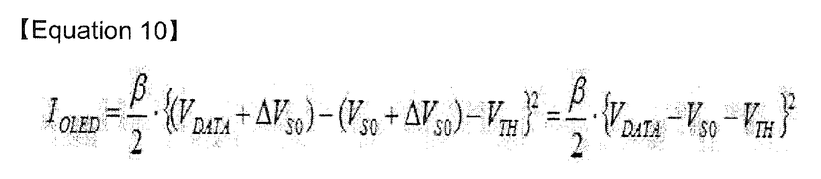
- Here, it can be seen that the current on the display panel regions currently performing a light emitting operation is not varied. Accordingly, the problem of the Vss rising is solved, thereby not causing non-uniformity of a brightness according to each position on the
large display panel 30. - The lower power supply voltages (Vss[1]∼Vss[k]) are respectively supplied to the corresponding lower power supply voltage supply lines in the display panel regions (30A∼30K) by being diverged as shown in
FIG. 10B . For instance, in thedisplay panel region 30A, the lower power supply voltage (Vss1) is diverged into 76 lower power supply voltages in the same manner asFIG. 10B , and is supplied to the corresponding lower power supply voltage supply line. -
FIGS. 11A to 11E are timing diagrams showing a data voltage programming period (P1), a data voltage emission period (P2), scan signals, and data voltages on the display panel regions (30A∼30K) to which the lower power supply voltages (Vss[1]∼Vss[k]) are respectively supplied. - More concretely,
FIGS. 11A and 11B show examples of the data voltage programming period (P1) and the data voltage emission period (P2) with respect to each of the display panel regions (30A∼30K). When thedisplay panel 30 is defined as 10 display panel regions (30A∼30K), 1/10 of one frame period is set as the data voltage programming period (P1) with respect to each of the display panel regions (30A∼30K), and the rest 9/10of the one frame period is set as the data voltage emission period (P2). -
FIGS. 11C and 11D are timing diagrams showing scan signals with respect to each of the display panel regions (30A∼30K), which are same as general timing diagrams. -
FIG. 11E is a timing diagram showing data voltages supplied through data lines (D1∼Dn) with respect to each of the display panel regions (30A∼30K), which are same as a general timing diagram. - With taking the pixel circuit of
FIG. 4B and the display region (30A) among the display panel regions (30A∼30K) on thedisplay panel 30 as examples, data voltage programming and emission operations will be explained. - The data voltage programming period (P1) is set with respect to the first display panel region (30A) including all the pixels (PXs) connected to first to 76th scan lines (G1∼G76).
- As shown in
FIG. 11A , since a switching control signal (EMS[1]) of a 'low' level is applied to the gate of the switching transistor (T43) inside all the pixels (PXs) connected to the first to 76th scan lines (G1∼G76), the switching transistor (T43) is turned-OFF. Accordingly, the lower power supply voltage (Vss) from the lower power supply voltage supply line is not supplied to the corresponding pixel (PX). - As shown in
FIGS. 11C and 11D , the 76 scan signals (Scan[1]∼Scan[76]) are sequentially supplied to the first to 76th scan lines (G1∼G76) in the data voltage programming period (P1), thereby turning-ON the switching transistors (T41) connected to the scan signals inside all the pixels (PXs). Here, data voltages (DATA) are supplied to the switching transistors (T41) through the data lines (D1∼Dm). The data voltage (DATA) is charged to each storage capacitor (C41) through the switching transistors (T41) inside the respective pixels (PXs), and is maintained for the data voltage emission period (P2). - The data voltage programming and emission operations for the other display panel regions (30B∼30K) are performed in the same manner as the
display panel region 30A. - Accordingly, the data voltage programming period and the lighting duration of the organic light emitting diode can be sufficiently obtained regardless of the size of the
display panel 30. - In the pixel driving method and apparatus for an organic light emitting device according to the present invention, in the data voltage programming period, a data voltage of a desired level can be precisely charged by charging the data voltage to the storage capacitor in a state that supply of the power supply voltage supplied to the organic light emitting diode (OLED) is cut-off. Also, in the data voltage emission period, the power supply to the OLED is started, thereby preventing a driving voltage of the driving transistor from changing. Accordingly, a non-uniform brightness of the OLED is solved.
- The foregoing embodiments and advantages are merely exemplary and are not to be construed as limiting the present disclosure. The present teachings can be readily applied to other types of apparatuses. This description is intended to be illustrative, and not to limit the scope of the claims. Many alternatives, modifications, and variations will be apparent to those skilled in the art. The features, structures, methods, and other characteristics of the exemplary embodiments described herein may be combined in various ways to obtain additional and/or alternative exemplary embodiments.
- As the present features may be embodied in several forms without departing from the characteristics thereof, it should also be understood that the above-described embodiments are not limited by any of the details of the foregoing description, unless otherwise specified, but rather should be construed broadly within its scope as defined in the appended claims, and therefore all changes and modifications that fall within the metes and bounds of the claims, or equivalents of such metes and bounds are therefore intended to be embraced by the appended claims.
Claims (20)
- A pixel driving method for an organic light emitting device, comprising:a first step of charging a data voltage supplied through a data line to a storage capacitor by driving an N-channel switching transistor, when cutting off supply of an upper power supply voltage to an organic light emitting diode ; anda second step of making the organic light emitting diode emit light by driving the N-channel driving transistor by the data voltage charged to the storage capacitor, when supplying the upper power supply voltage.
- The method of claim 1, wherein the N-channel switching transistor is driven by positive scan signals.
- The method of claim 1, wherein the storage capacitor is connected between a gate terminal of the N-channel driving transistor and a lower power supply voltage terminal.
- The method of claim 3, wherein the lower power supply voltage terminal is connected to a lower power supply voltage supply line having a mesh structure.
- The method of claim 1, wherein the storage capacitor is connected between a gate terminal and a source terminal of the N-channel driving transistor.
- The method of claim 1, wherein the organic light emitting diode has an anode connected to an upper power supply voltage terminal, and a cathode connected to a drain of the N-channel driving transistor.
- The method of claim 1, wherein the organic light emitting diode has an anode connected to a source terminal of the N-channel driving transistor, and a cathode connected to a lower power supply voltage terminal.
- The method of claim 1, wherein supply or cut-off of the upper power supply voltage to the organic light emitting diode is controlled by a switching transistor connected between the organic light emitting diode and the driving transistor.
- A pixel driving method for an organic light emitting device, comprising:a first step of charging a data voltage supplied through a data line to a storage capacitor by driving a P-channel switching transistor, when cutting off supply of a lower power supply voltage to an organic light emitting diode; anda second step of making the organic light emitting diode emit light by driving the P-channel driving transistor by the data voltage charged to the storage capacitor, when supplying the lower power supply voltage.
- The method of claim 9, wherein the P-channel switching transistor is driven by negative scan signals.
- The method of claim 9, wherein the storage capacitor is connected between a gate terminal of the P-channel driving transistor and an upper power supply voltage terminal.
- The method of claim 9, wherein the organic light emitting diode has an anode connected to a source terminal of the P-channel driving transistor, and a cathode connected to a lower power supply voltage terminal.
- The method of claim 9, wherein supply or cut-off of the lower power supply voltage to the organic light emitting diode is controlled by a switching transistor connected between the organic light emitting diode and the driving transistor.
- A pixel driving method for an organic light emitting device, comprising:defining a display panel of the organic light emitting device into a plurality of display panel regions in a horizontal direction such that a plurality of adjacent scan lines can be included in each region;making pixels inside each of the plurality of display panel regions share one lower power supply voltage among a plurality of lower power supply voltages supplied from a lower power supply voltage supply terminal by being diverged; anddetermining a data voltage programming period and a data voltage emission period in one frame period according to each of the display panel regions.
- The method of claim 14, wherein the plurality of lower power supply voltages are supplied by being diverged from one common point.
- The method of claim 14, wherein scan signals are sequentially supplied to the scan lines in one frame period.
- The method of claim 14, wherein the data voltage programming period is determined by dividing the one frame period by the number of the display panel regions.
- The method of claim 14, wherein the data voltage emission period corresponds to other period except the data voltage programming period in one frame period.
- A pixel driving apparatus for an organic light emitting device, comprising;a first switching transistor for transmitting data voltages supplied through data lines to a storage capacitor by being driven by scan signals, in a state that supply of an upper power supply voltage is cut-off;a storage capacitor for charging the data voltage, in a state that supply of the upper power supply voltage is cut-off, by being connected between a gate terminal of a driving transistor and a lower power supply voltage terminal;a driving transistor for supplying a driving current corresponding to the data voltage charged to the storage capacitor to an organic light emitting diode, in a state that the upper power supply voltage is supplied;a second switching transistor being turned-off by a switching control signal of a 'low' level in the time of supplying scan signals by being connected between the cathode of the OLED and the drain of the driving transistor;an organic light emitting diode for emitting light with a brightness corresponding to the driving current by having an anode connected to the upper power supply voltage and a cathode connected to a drain of the second switching transistor.
- A pixel driving apparatus for an organic light emitting device, comprising a display panel,
wherein the display panel is configured to:define a plurality of display panel regions in a horizontal direction such that a plurality of adjacent scan lines can be included in each region;make pixels inside each of the plurality of display panel regions share one lower power supply voltage among a plurality of lower power supply voltages supplied by being diverged; anddetermine a data voltage programming period and a data voltage emission period in one frame period according to each of the display panel regions.
Applications Claiming Priority (1)
| Application Number | Priority Date | Filing Date | Title |
|---|---|---|---|
| KR1020070096141A KR20080090954A (en) | 2007-04-06 | 2007-09-20 | Pixel driving method and apparatus of organic light emitting display device |
Publications (2)
| Publication Number | Publication Date |
|---|---|
| EP2040248A2 true EP2040248A2 (en) | 2009-03-25 |
| EP2040248A3 EP2040248A3 (en) | 2010-07-28 |
Family
ID=40114419
Family Applications (1)
| Application Number | Title | Priority Date | Filing Date |
|---|---|---|---|
| EP07124161A Ceased EP2040248A3 (en) | 2007-09-20 | 2007-12-28 | Pixel driving method and apparatus for organic light emitting device |
Country Status (3)
| Country | Link |
|---|---|
| US (1) | US8264428B2 (en) |
| EP (1) | EP2040248A3 (en) |
| CN (1) | CN101393721B (en) |
Families Citing this family (32)
| Publication number | Priority date | Publication date | Assignee | Title |
|---|---|---|---|---|
| KR101056281B1 (en) * | 2009-08-03 | 2011-08-11 | 삼성모바일디스플레이주식회사 | Organic electroluminescent display and driving method thereof |
| FR2949007B1 (en) | 2009-08-07 | 2012-06-08 | Nanotec Solution | DEVICE AND METHOD FOR CONTROL INTERFACE SENSITIVE TO A MOVEMENT OF A BODY OR OBJECT AND CONTROL EQUIPMENT INCORPORATING THIS DEVICE. |
| KR101182238B1 (en) * | 2010-06-28 | 2012-09-12 | 삼성디스플레이 주식회사 | Organic Light Emitting Display and Driving Method Thereof |
| FR2976688B1 (en) | 2011-06-16 | 2021-04-23 | Nanotec Solution | DEVICE AND METHOD FOR GENERATING AN ELECTRICAL POWER SUPPLY IN AN ELECTRONIC SYSTEM WITH A VARIABLE REFERENCE POTENTIAL. |
| JP5891492B2 (en) * | 2011-06-22 | 2016-03-23 | 株式会社Joled | Display element, display device, and electronic device |
| KR101396004B1 (en) * | 2011-08-17 | 2014-05-16 | 엘지디스플레이 주식회사 | Organic light emitting diode display device |
| CN102654975B (en) * | 2011-11-01 | 2014-08-20 | 京东方科技集团股份有限公司 | AMOLED (active matrix/organic light emitting diode) drive compensation circuit and method and display device thereof |
| FR2985049B1 (en) | 2011-12-22 | 2014-01-31 | Nanotec Solution | CAPACITIVE MEASURING DEVICE WITH SWITCHED ELECTRODES FOR TOUCHLESS CONTACTLESS INTERFACES |
| CN102655703B (en) * | 2012-03-23 | 2014-09-24 | 华映视讯(吴江)有限公司 | Driving circuit of organic light-emitting diode |
| US9336723B2 (en) | 2013-02-13 | 2016-05-10 | Apple Inc. | In-cell touch for LED |
| WO2015088629A1 (en) | 2013-12-13 | 2015-06-18 | Pylemta Management Llc | Integrated touch and display architectures for self-capacitive touch sensors |
| WO2015175013A1 (en) | 2014-05-16 | 2015-11-19 | Wrostix Technologies Llc | Structure for integrated touch screen |
| US10936120B2 (en) | 2014-05-22 | 2021-03-02 | Apple Inc. | Panel bootstraping architectures for in-cell self-capacitance |
| CN105810145B (en) * | 2014-12-30 | 2018-06-26 | 昆山工研院新型平板显示技术中心有限公司 | Pixel, the driving method of pixel and organic light emitting display |
| EP3508959A1 (en) | 2015-02-02 | 2019-07-10 | Apple Inc. | Flexible self-capacitance and mutual capacitance touch sensing system architecture |
| CN104916660B (en) * | 2015-04-20 | 2018-04-20 | 京东方科技集团股份有限公司 | Flexible display panels and display device |
| WO2018023089A1 (en) | 2016-07-29 | 2018-02-01 | Apple Inc. | Touch sensor panel with multi-power domain chip configuration |
| US11335301B2 (en) * | 2017-06-30 | 2022-05-17 | Kunshan Go-Visionox Opto-Electronics Co., Ltd. | Devices and methods for dimming a display screen |
| CN107301840B (en) * | 2017-08-11 | 2020-04-14 | 京东方科技集团股份有限公司 | A pixel compensation circuit and method, display driving device and display device |
| JP6512259B1 (en) * | 2017-10-30 | 2019-05-15 | セイコーエプソン株式会社 | Electro-optical device and electronic apparatus |
| CN108492775B (en) * | 2018-05-14 | 2020-03-17 | 昆山国显光电有限公司 | Array substrate, display screen and display device |
| KR102655012B1 (en) * | 2018-09-12 | 2024-04-08 | 엘지디스플레이 주식회사 | Gate driving circuit, display panel, display device |
| US10902793B2 (en) * | 2018-09-12 | 2021-01-26 | Lg Display Co., Ltd. | Gate driver circuit outputting a plurality of emission signals having different delay times or pulse widths or combinations thereof |
| US10984712B2 (en) * | 2018-12-10 | 2021-04-20 | Sharp Kabushiki Kaisha | TFT pixel circuit for OLED external compensation using an adjusted data voltage for component compensation |
| CN210378422U (en) * | 2019-11-27 | 2020-04-21 | 京东方科技集团股份有限公司 | Pixel circuit and display device |
| CN111583862B (en) * | 2020-05-19 | 2022-07-12 | 深圳市华星光电半导体显示技术有限公司 | Pixel driving circuit and OLED display panel |
| US11662867B1 (en) | 2020-05-30 | 2023-05-30 | Apple Inc. | Hover detection on a touch sensor panel |
| CN112259049A (en) * | 2020-10-30 | 2021-01-22 | 合肥京东方卓印科技有限公司 | Display control method and device |
| KR102896834B1 (en) * | 2021-09-01 | 2025-12-08 | 삼성디스플레이 주식회사 | Pixel circuit and display device using the same |
| KR20230102885A (en) * | 2021-12-30 | 2023-07-07 | 엘지디스플레이 주식회사 | Light Emitting Display Device and Driving Method of the same |
| US20250089488A1 (en) * | 2022-11-30 | 2025-03-13 | Chongqing Boe Display Technology Co., Ltd. | Display panel and display apparatus |
| KR20250014141A (en) * | 2023-07-19 | 2025-02-03 | 엘지디스플레이 주식회사 | Display Device and Driving Method of the same |
Family Cites Families (22)
| Publication number | Priority date | Publication date | Assignee | Title |
|---|---|---|---|---|
| GB9925060D0 (en) * | 1999-10-23 | 1999-12-22 | Koninkl Philips Electronics Nv | Active matrix electroluminescent display device |
| JP3800404B2 (en) | 2001-12-19 | 2006-07-26 | 株式会社日立製作所 | Image display device |
| KR100878269B1 (en) * | 2002-06-18 | 2009-01-13 | 삼성전자주식회사 | Liquid crystal display with time division color display method, driving method and backlight device |
| TW584820B (en) * | 2003-02-11 | 2004-04-21 | Au Optronics Corp | Organic light emitting display |
| US7122969B2 (en) * | 2003-06-18 | 2006-10-17 | Semiconductor Energy Laboratory Co., Ltd. | Element substrate and light emitting device |
| KR101080350B1 (en) * | 2004-04-07 | 2011-11-04 | 삼성전자주식회사 | Display device and method of driving thereof |
| KR20050115346A (en) | 2004-06-02 | 2005-12-07 | 삼성전자주식회사 | Display device and driving method thereof |
| DE102004028233A1 (en) * | 2004-06-11 | 2005-12-29 | Deutsche Thomson-Brandt Gmbh | Method for controlling and switching an element of a light-emitting display |
| KR101080351B1 (en) * | 2004-06-22 | 2011-11-04 | 삼성전자주식회사 | Display device and driving method thereof |
| JP4889205B2 (en) * | 2004-06-30 | 2012-03-07 | グローバル・オーエルイーディー・テクノロジー・リミテッド・ライアビリティ・カンパニー | Active matrix display device |
| KR100592641B1 (en) * | 2004-07-28 | 2006-06-26 | 삼성에스디아이 주식회사 | Pixel circuit and organic light emitting display device |
| KR100604066B1 (en) * | 2004-12-24 | 2006-07-24 | 삼성에스디아이 주식회사 | Pixel and light emitting display device using same |
| KR100613088B1 (en) * | 2004-12-24 | 2006-08-16 | 삼성에스디아이 주식회사 | Data integrated circuit and light emitting display device using the same |
| KR100748739B1 (en) * | 2005-01-28 | 2007-08-13 | 도시바 마쯔시따 디스플레이 테크놀로지 컴퍼니, 리미티드 | El display apparatus and method of driving the same |
| KR100762138B1 (en) * | 2005-05-17 | 2007-10-02 | 엘지전자 주식회사 | Driving Method of Flat Panel Display Panel |
| US7868880B2 (en) | 2005-05-24 | 2011-01-11 | Casio Computer Co., Ltd. | Display apparatus and drive control method thereof |
| JP4752331B2 (en) * | 2005-05-25 | 2011-08-17 | セイコーエプソン株式会社 | Light emitting device, driving method and driving circuit thereof, and electronic apparatus |
| TW200707385A (en) * | 2005-07-15 | 2007-02-16 | Seiko Epson Corp | Electronic device, method of driving the same, electro-optical device, and electronic apparatus |
| KR20070071725A (en) | 2005-12-30 | 2007-07-04 | 엘지.필립스 엘시디 주식회사 | Driving device of liquid crystal display device |
| TWI279763B (en) * | 2006-03-13 | 2007-04-21 | Himax Tech Ltd | Light emitting display, pixel circuit and driving method thereof |
| KR101194861B1 (en) * | 2006-06-01 | 2012-10-26 | 엘지디스플레이 주식회사 | Organic light emitting diode display |
| KR101040816B1 (en) * | 2009-02-27 | 2011-06-13 | 삼성모바일디스플레이주식회사 | Pixel and organic light emitting display device using same |
-
2007
- 2007-12-28 EP EP07124161A patent/EP2040248A3/en not_active Ceased
- 2007-12-28 US US12/003,627 patent/US8264428B2/en active Active
- 2007-12-29 CN CN200710308335XA patent/CN101393721B/en active Active
Also Published As
| Publication number | Publication date |
|---|---|
| CN101393721B (en) | 2013-06-05 |
| EP2040248A3 (en) | 2010-07-28 |
| US8264428B2 (en) | 2012-09-11 |
| US20090079679A1 (en) | 2009-03-26 |
| CN101393721A (en) | 2009-03-25 |
Similar Documents
| Publication | Publication Date | Title |
|---|---|---|
| US8264428B2 (en) | Pixel driving method and apparatus for organic light emitting device | |
| EP2232557B1 (en) | Pixel circuit | |
| US7236149B2 (en) | Pixel circuit, display device, and driving method of pixel circuit | |
| US7561128B2 (en) | Organic electroluminescence display device | |
| KR100684514B1 (en) | Drive circuit and display device | |
| US10607541B2 (en) | Display device and electronic apparatus | |
| US7554514B2 (en) | Electro-optical device and electronic apparatus | |
| KR101014899B1 (en) | Organic light emitting display device | |
| JP4984715B2 (en) | Display device driving method and display element driving method | |
| KR101800917B1 (en) | Image display device | |
| US7825881B2 (en) | Organic light emitting display device | |
| US20060132055A1 (en) | Organic light emitting display and method of fabricating the same | |
| CN100403377C (en) | image display device | |
| KR20040104399A (en) | A pixel circuit and display device | |
| US20060256058A1 (en) | Pixel circuit, display device method for controlling pixel circuit | |
| JP2010281914A (en) | Display device, display device driving method, and electronic apparatus | |
| US9076380B2 (en) | Pixel driving cirucit, pixel driving methods, display panels and electronic devices | |
| JP2008032863A5 (en) | ||
| JP7253796B2 (en) | Pixel circuit and display device | |
| JP2021067901A (en) | Pixel circuit and display device | |
| US20120194501A1 (en) | Image display device | |
| KR20080090954A (en) | Pixel driving method and apparatus of organic light emitting display device | |
| US8570309B2 (en) | Buffer and organic light emitting display using the same | |
| JP2008286897A (en) | Display device, display device driving method, and electronic apparatus | |
| US7212179B2 (en) | Light emitting display device, electronic equipment into which the same device is loaded, and drive method of the light emitting display device |
Legal Events
| Date | Code | Title | Description |
|---|---|---|---|
| PUAI | Public reference made under article 153(3) epc to a published international application that has entered the european phase |
Free format text: ORIGINAL CODE: 0009012 |
|
| 17P | Request for examination filed |
Effective date: 20071228 |
|
| AK | Designated contracting states |
Kind code of ref document: A2 Designated state(s): AT BE BG CH CY CZ DE DK EE ES FI FR GB GR HU IE IS IT LI LT LU LV MC MT NL PL PT RO SE SI SK TR |
|
| AX | Request for extension of the european patent |
Extension state: AL BA HR MK RS |
|
| PUAL | Search report despatched |
Free format text: ORIGINAL CODE: 0009013 |
|
| AK | Designated contracting states |
Kind code of ref document: A3 Designated state(s): AT BE BG CH CY CZ DE DK EE ES FI FR GB GR HU IE IS IT LI LT LU LV MC MT NL PL PT RO SE SI SK TR |
|
| AX | Request for extension of the european patent |
Extension state: AL BA HR MK RS |
|
| AKX | Designation fees paid |
Designated state(s): AT BE BG CH CY CZ DE DK EE ES FI FR GB GR HU IE IS IT LI LT LU LV MC MT NL PL PT RO SE SI SK TR |
|
| 17Q | First examination report despatched |
Effective date: 20110523 |
|
| APBK | Appeal reference recorded |
Free format text: ORIGINAL CODE: EPIDOSNREFNE |
|
| APBN | Date of receipt of notice of appeal recorded |
Free format text: ORIGINAL CODE: EPIDOSNNOA2E |
|
| APBR | Date of receipt of statement of grounds of appeal recorded |
Free format text: ORIGINAL CODE: EPIDOSNNOA3E |
|
| APAF | Appeal reference modified |
Free format text: ORIGINAL CODE: EPIDOSCREFNE |
|
| APBT | Appeal procedure closed |
Free format text: ORIGINAL CODE: EPIDOSNNOA9E |
|
| STAA | Information on the status of an ep patent application or granted ep patent |
Free format text: STATUS: THE APPLICATION HAS BEEN REFUSED |
|
| 18R | Application refused |
Effective date: 20171211 |
|
| R18R | Application refused (corrected) |
Effective date: 20180426 |