EP2039729A2 - Anisotropic magnetic flakes - Google Patents
Anisotropic magnetic flakes Download PDFInfo
- Publication number
- EP2039729A2 EP2039729A2 EP08164504A EP08164504A EP2039729A2 EP 2039729 A2 EP2039729 A2 EP 2039729A2 EP 08164504 A EP08164504 A EP 08164504A EP 08164504 A EP08164504 A EP 08164504A EP 2039729 A2 EP2039729 A2 EP 2039729A2
- Authority
- EP
- European Patent Office
- Prior art keywords
- flakes
- magnetic
- substrate
- coating
- flake
- Prior art date
- Legal status (The legal status is an assumption and is not a legal conclusion. Google has not performed a legal analysis and makes no representation as to the accuracy of the status listed.)
- Granted
Links
Images


Classifications
-
- C—CHEMISTRY; METALLURGY
- C09—DYES; PAINTS; POLISHES; NATURAL RESINS; ADHESIVES; COMPOSITIONS NOT OTHERWISE PROVIDED FOR; APPLICATIONS OF MATERIALS NOT OTHERWISE PROVIDED FOR
- C09D—COATING COMPOSITIONS, e.g. PAINTS, VARNISHES OR LACQUERS; FILLING PASTES; CHEMICAL PAINT OR INK REMOVERS; INKS; CORRECTING FLUIDS; WOODSTAINS; PASTES OR SOLIDS FOR COLOURING OR PRINTING; USE OF MATERIALS THEREFOR
- C09D7/00—Features of coating compositions, not provided for in group C09D5/00; Processes for incorporating ingredients in coating compositions
- C09D7/40—Additives
- C09D7/60—Additives non-macromolecular
- C09D7/61—Additives non-macromolecular inorganic
-
- B—PERFORMING OPERATIONS; TRANSPORTING
- B42—BOOKBINDING; ALBUMS; FILES; SPECIAL PRINTED MATTER
- B42D—BOOKS; BOOK COVERS; LOOSE LEAVES; PRINTED MATTER CHARACTERISED BY IDENTIFICATION OR SECURITY FEATURES; PRINTED MATTER OF SPECIAL FORMAT OR STYLE NOT OTHERWISE PROVIDED FOR; DEVICES FOR USE THEREWITH AND NOT OTHERWISE PROVIDED FOR; MOVABLE-STRIP WRITING OR READING APPARATUS
- B42D25/00—Information-bearing cards or sheet-like structures characterised by identification or security features; Manufacture thereof
- B42D25/20—Information-bearing cards or sheet-like structures characterised by identification or security features; Manufacture thereof characterised by a particular use or purpose
- B42D25/29—Securities; Bank notes
-
- B—PERFORMING OPERATIONS; TRANSPORTING
- B42—BOOKBINDING; ALBUMS; FILES; SPECIAL PRINTED MATTER
- B42D—BOOKS; BOOK COVERS; LOOSE LEAVES; PRINTED MATTER CHARACTERISED BY IDENTIFICATION OR SECURITY FEATURES; PRINTED MATTER OF SPECIAL FORMAT OR STYLE NOT OTHERWISE PROVIDED FOR; DEVICES FOR USE THEREWITH AND NOT OTHERWISE PROVIDED FOR; MOVABLE-STRIP WRITING OR READING APPARATUS
- B42D25/00—Information-bearing cards or sheet-like structures characterised by identification or security features; Manufacture thereof
- B42D25/30—Identification or security features, e.g. for preventing forgery
- B42D25/328—Diffraction gratings; Holograms
-
- B—PERFORMING OPERATIONS; TRANSPORTING
- B42—BOOKBINDING; ALBUMS; FILES; SPECIAL PRINTED MATTER
- B42D—BOOKS; BOOK COVERS; LOOSE LEAVES; PRINTED MATTER CHARACTERISED BY IDENTIFICATION OR SECURITY FEATURES; PRINTED MATTER OF SPECIAL FORMAT OR STYLE NOT OTHERWISE PROVIDED FOR; DEVICES FOR USE THEREWITH AND NOT OTHERWISE PROVIDED FOR; MOVABLE-STRIP WRITING OR READING APPARATUS
- B42D25/00—Information-bearing cards or sheet-like structures characterised by identification or security features; Manufacture thereof
- B42D25/30—Identification or security features, e.g. for preventing forgery
- B42D25/36—Identification or security features, e.g. for preventing forgery comprising special materials
- B42D25/369—Magnetised or magnetisable materials
-
- B—PERFORMING OPERATIONS; TRANSPORTING
- B82—NANOTECHNOLOGY
- B82Y—SPECIFIC USES OR APPLICATIONS OF NANOSTRUCTURES; MEASUREMENT OR ANALYSIS OF NANOSTRUCTURES; MANUFACTURE OR TREATMENT OF NANOSTRUCTURES
- B82Y30/00—Nanotechnology for materials or surface science, e.g. nanocomposites
-
- C—CHEMISTRY; METALLURGY
- C09—DYES; PAINTS; POLISHES; NATURAL RESINS; ADHESIVES; COMPOSITIONS NOT OTHERWISE PROVIDED FOR; APPLICATIONS OF MATERIALS NOT OTHERWISE PROVIDED FOR
- C09C—TREATMENT OF INORGANIC MATERIALS, OTHER THAN FIBROUS FILLERS, TO ENHANCE THEIR PIGMENTING OR FILLING PROPERTIES ; PREPARATION OF CARBON BLACK ; PREPARATION OF INORGANIC MATERIALS WHICH ARE NO SINGLE CHEMICAL COMPOUNDS AND WHICH ARE MAINLY USED AS PIGMENTS OR FILLERS
- C09C1/00—Treatment of specific inorganic materials other than fibrous fillers; Preparation of carbon black
- C09C1/0015—Pigments exhibiting interference colours, e.g. transparent platelets of appropriate thinness or flaky substrates, e.g. mica, bearing appropriate thin transparent coatings
- C09C1/0021—Pigments exhibiting interference colours, e.g. transparent platelets of appropriate thinness or flaky substrates, e.g. mica, bearing appropriate thin transparent coatings comprising a core coated with only one layer having a high or low refractive index
-
- C—CHEMISTRY; METALLURGY
- C09—DYES; PAINTS; POLISHES; NATURAL RESINS; ADHESIVES; COMPOSITIONS NOT OTHERWISE PROVIDED FOR; APPLICATIONS OF MATERIALS NOT OTHERWISE PROVIDED FOR
- C09C—TREATMENT OF INORGANIC MATERIALS, OTHER THAN FIBROUS FILLERS, TO ENHANCE THEIR PIGMENTING OR FILLING PROPERTIES ; PREPARATION OF CARBON BLACK ; PREPARATION OF INORGANIC MATERIALS WHICH ARE NO SINGLE CHEMICAL COMPOUNDS AND WHICH ARE MAINLY USED AS PIGMENTS OR FILLERS
- C09C1/00—Treatment of specific inorganic materials other than fibrous fillers; Preparation of carbon black
- C09C1/0078—Pigments consisting of flaky, non-metallic substrates, characterised by a surface-region containing free metal
-
- C—CHEMISTRY; METALLURGY
- C09—DYES; PAINTS; POLISHES; NATURAL RESINS; ADHESIVES; COMPOSITIONS NOT OTHERWISE PROVIDED FOR; APPLICATIONS OF MATERIALS NOT OTHERWISE PROVIDED FOR
- C09D—COATING COMPOSITIONS, e.g. PAINTS, VARNISHES OR LACQUERS; FILLING PASTES; CHEMICAL PAINT OR INK REMOVERS; INKS; CORRECTING FLUIDS; WOODSTAINS; PASTES OR SOLIDS FOR COLOURING OR PRINTING; USE OF MATERIALS THEREFOR
- C09D11/00—Inks
- C09D11/02—Printing inks
- C09D11/03—Printing inks characterised by features other than the chemical nature of the binder
- C09D11/037—Printing inks characterised by features other than the chemical nature of the binder characterised by the pigment
-
- C—CHEMISTRY; METALLURGY
- C09—DYES; PAINTS; POLISHES; NATURAL RESINS; ADHESIVES; COMPOSITIONS NOT OTHERWISE PROVIDED FOR; APPLICATIONS OF MATERIALS NOT OTHERWISE PROVIDED FOR
- C09D—COATING COMPOSITIONS, e.g. PAINTS, VARNISHES OR LACQUERS; FILLING PASTES; CHEMICAL PAINT OR INK REMOVERS; INKS; CORRECTING FLUIDS; WOODSTAINS; PASTES OR SOLIDS FOR COLOURING OR PRINTING; USE OF MATERIALS THEREFOR
- C09D11/00—Inks
- C09D11/50—Sympathetic, colour changing or similar inks
-
- C—CHEMISTRY; METALLURGY
- C09—DYES; PAINTS; POLISHES; NATURAL RESINS; ADHESIVES; COMPOSITIONS NOT OTHERWISE PROVIDED FOR; APPLICATIONS OF MATERIALS NOT OTHERWISE PROVIDED FOR
- C09D—COATING COMPOSITIONS, e.g. PAINTS, VARNISHES OR LACQUERS; FILLING PASTES; CHEMICAL PAINT OR INK REMOVERS; INKS; CORRECTING FLUIDS; WOODSTAINS; PASTES OR SOLIDS FOR COLOURING OR PRINTING; USE OF MATERIALS THEREFOR
- C09D201/00—Coating compositions based on unspecified macromolecular compounds
-
- C—CHEMISTRY; METALLURGY
- C09—DYES; PAINTS; POLISHES; NATURAL RESINS; ADHESIVES; COMPOSITIONS NOT OTHERWISE PROVIDED FOR; APPLICATIONS OF MATERIALS NOT OTHERWISE PROVIDED FOR
- C09D—COATING COMPOSITIONS, e.g. PAINTS, VARNISHES OR LACQUERS; FILLING PASTES; CHEMICAL PAINT OR INK REMOVERS; INKS; CORRECTING FLUIDS; WOODSTAINS; PASTES OR SOLIDS FOR COLOURING OR PRINTING; USE OF MATERIALS THEREFOR
- C09D5/00—Coating compositions, e.g. paints, varnishes or lacquers, characterised by their physical nature or the effects produced; Filling pastes
- C09D5/004—Reflecting paints; Signal paints
-
- C—CHEMISTRY; METALLURGY
- C09—DYES; PAINTS; POLISHES; NATURAL RESINS; ADHESIVES; COMPOSITIONS NOT OTHERWISE PROVIDED FOR; APPLICATIONS OF MATERIALS NOT OTHERWISE PROVIDED FOR
- C09D—COATING COMPOSITIONS, e.g. PAINTS, VARNISHES OR LACQUERS; FILLING PASTES; CHEMICAL PAINT OR INK REMOVERS; INKS; CORRECTING FLUIDS; WOODSTAINS; PASTES OR SOLIDS FOR COLOURING OR PRINTING; USE OF MATERIALS THEREFOR
- C09D7/00—Features of coating compositions, not provided for in group C09D5/00; Processes for incorporating ingredients in coating compositions
- C09D7/40—Additives
- C09D7/70—Additives characterised by shape, e.g. fibres, flakes or microspheres
-
- H—ELECTRICITY
- H01—ELECTRIC ELEMENTS
- H01F—MAGNETS; INDUCTANCES; TRANSFORMERS; SELECTION OF MATERIALS FOR THEIR MAGNETIC PROPERTIES
- H01F1/00—Magnets or magnetic bodies characterised by the magnetic materials therefor; Selection of materials for their magnetic properties
- H01F1/0027—Thick magnetic films
-
- H—ELECTRICITY
- H01—ELECTRIC ELEMENTS
- H01F—MAGNETS; INDUCTANCES; TRANSFORMERS; SELECTION OF MATERIALS FOR THEIR MAGNETIC PROPERTIES
- H01F10/00—Thin magnetic films, e.g. of one-domain structure
- H01F10/08—Thin magnetic films, e.g. of one-domain structure characterised by magnetic layers
-
- B42D2033/16—
-
- B42D2033/18—
-
- B42D2035/14—
-
- C—CHEMISTRY; METALLURGY
- C01—INORGANIC CHEMISTRY
- C01P—INDEXING SCHEME RELATING TO STRUCTURAL AND PHYSICAL ASPECTS OF SOLID INORGANIC COMPOUNDS
- C01P2004/00—Particle morphology
- C01P2004/01—Particle morphology depicted by an image
- C01P2004/02—Particle morphology depicted by an image obtained by optical microscopy
-
- C—CHEMISTRY; METALLURGY
- C01—INORGANIC CHEMISTRY
- C01P—INDEXING SCHEME RELATING TO STRUCTURAL AND PHYSICAL ASPECTS OF SOLID INORGANIC COMPOUNDS
- C01P2004/00—Particle morphology
- C01P2004/01—Particle morphology depicted by an image
- C01P2004/03—Particle morphology depicted by an image obtained by SEM
-
- C—CHEMISTRY; METALLURGY
- C01—INORGANIC CHEMISTRY
- C01P—INDEXING SCHEME RELATING TO STRUCTURAL AND PHYSICAL ASPECTS OF SOLID INORGANIC COMPOUNDS
- C01P2004/00—Particle morphology
- C01P2004/60—Particles characterised by their size
- C01P2004/61—Micrometer sized, i.e. from 1-100 micrometer
-
- C—CHEMISTRY; METALLURGY
- C01—INORGANIC CHEMISTRY
- C01P—INDEXING SCHEME RELATING TO STRUCTURAL AND PHYSICAL ASPECTS OF SOLID INORGANIC COMPOUNDS
- C01P2004/00—Particle morphology
- C01P2004/60—Particles characterised by their size
- C01P2004/62—Submicrometer sized, i.e. from 0.1-1 micrometer
-
- C—CHEMISTRY; METALLURGY
- C01—INORGANIC CHEMISTRY
- C01P—INDEXING SCHEME RELATING TO STRUCTURAL AND PHYSICAL ASPECTS OF SOLID INORGANIC COMPOUNDS
- C01P2004/00—Particle morphology
- C01P2004/60—Particles characterised by their size
- C01P2004/64—Nanometer sized, i.e. from 1-100 nanometer
-
- C—CHEMISTRY; METALLURGY
- C01—INORGANIC CHEMISTRY
- C01P—INDEXING SCHEME RELATING TO STRUCTURAL AND PHYSICAL ASPECTS OF SOLID INORGANIC COMPOUNDS
- C01P2006/00—Physical properties of inorganic compounds
- C01P2006/42—Magnetic properties
-
- C—CHEMISTRY; METALLURGY
- C01—INORGANIC CHEMISTRY
- C01P—INDEXING SCHEME RELATING TO STRUCTURAL AND PHYSICAL ASPECTS OF SOLID INORGANIC COMPOUNDS
- C01P2006/00—Physical properties of inorganic compounds
- C01P2006/60—Optical properties, e.g. expressed in CIELAB-values
-
- C—CHEMISTRY; METALLURGY
- C09—DYES; PAINTS; POLISHES; NATURAL RESINS; ADHESIVES; COMPOSITIONS NOT OTHERWISE PROVIDED FOR; APPLICATIONS OF MATERIALS NOT OTHERWISE PROVIDED FOR
- C09C—TREATMENT OF INORGANIC MATERIALS, OTHER THAN FIBROUS FILLERS, TO ENHANCE THEIR PIGMENTING OR FILLING PROPERTIES ; PREPARATION OF CARBON BLACK ; PREPARATION OF INORGANIC MATERIALS WHICH ARE NO SINGLE CHEMICAL COMPOUNDS AND WHICH ARE MAINLY USED AS PIGMENTS OR FILLERS
- C09C2200/00—Compositional and structural details of pigments exhibiting interference colours
- C09C2200/10—Interference pigments characterized by the core material
- C09C2200/1054—Interference pigments characterized by the core material the core consisting of a metal
-
- C—CHEMISTRY; METALLURGY
- C09—DYES; PAINTS; POLISHES; NATURAL RESINS; ADHESIVES; COMPOSITIONS NOT OTHERWISE PROVIDED FOR; APPLICATIONS OF MATERIALS NOT OTHERWISE PROVIDED FOR
- C09C—TREATMENT OF INORGANIC MATERIALS, OTHER THAN FIBROUS FILLERS, TO ENHANCE THEIR PIGMENTING OR FILLING PROPERTIES ; PREPARATION OF CARBON BLACK ; PREPARATION OF INORGANIC MATERIALS WHICH ARE NO SINGLE CHEMICAL COMPOUNDS AND WHICH ARE MAINLY USED AS PIGMENTS OR FILLERS
- C09C2200/00—Compositional and structural details of pigments exhibiting interference colours
- C09C2200/30—Interference pigments characterised by the thickness of the core or layers thereon or by the total thickness of the final pigment particle
- C09C2200/304—Thickness of intermediate layers adjacent to the core, e.g. metallic layers, protective layers, rutilisation enhancing layers or reflective layers
-
- C—CHEMISTRY; METALLURGY
- C09—DYES; PAINTS; POLISHES; NATURAL RESINS; ADHESIVES; COMPOSITIONS NOT OTHERWISE PROVIDED FOR; APPLICATIONS OF MATERIALS NOT OTHERWISE PROVIDED FOR
- C09C—TREATMENT OF INORGANIC MATERIALS, OTHER THAN FIBROUS FILLERS, TO ENHANCE THEIR PIGMENTING OR FILLING PROPERTIES ; PREPARATION OF CARBON BLACK ; PREPARATION OF INORGANIC MATERIALS WHICH ARE NO SINGLE CHEMICAL COMPOUNDS AND WHICH ARE MAINLY USED AS PIGMENTS OR FILLERS
- C09C2200/00—Compositional and structural details of pigments exhibiting interference colours
- C09C2200/30—Interference pigments characterised by the thickness of the core or layers thereon or by the total thickness of the final pigment particle
- C09C2200/306—Thickness of an absorbing layer
-
- C—CHEMISTRY; METALLURGY
- C09—DYES; PAINTS; POLISHES; NATURAL RESINS; ADHESIVES; COMPOSITIONS NOT OTHERWISE PROVIDED FOR; APPLICATIONS OF MATERIALS NOT OTHERWISE PROVIDED FOR
- C09C—TREATMENT OF INORGANIC MATERIALS, OTHER THAN FIBROUS FILLERS, TO ENHANCE THEIR PIGMENTING OR FILLING PROPERTIES ; PREPARATION OF CARBON BLACK ; PREPARATION OF INORGANIC MATERIALS WHICH ARE NO SINGLE CHEMICAL COMPOUNDS AND WHICH ARE MAINLY USED AS PIGMENTS OR FILLERS
- C09C2200/00—Compositional and structural details of pigments exhibiting interference colours
- C09C2200/30—Interference pigments characterised by the thickness of the core or layers thereon or by the total thickness of the final pigment particle
- C09C2200/308—Total thickness of the pigment particle
-
- C—CHEMISTRY; METALLURGY
- C09—DYES; PAINTS; POLISHES; NATURAL RESINS; ADHESIVES; COMPOSITIONS NOT OTHERWISE PROVIDED FOR; APPLICATIONS OF MATERIALS NOT OTHERWISE PROVIDED FOR
- C09C—TREATMENT OF INORGANIC MATERIALS, OTHER THAN FIBROUS FILLERS, TO ENHANCE THEIR PIGMENTING OR FILLING PROPERTIES ; PREPARATION OF CARBON BLACK ; PREPARATION OF INORGANIC MATERIALS WHICH ARE NO SINGLE CHEMICAL COMPOUNDS AND WHICH ARE MAINLY USED AS PIGMENTS OR FILLERS
- C09C2200/00—Compositional and structural details of pigments exhibiting interference colours
- C09C2200/40—Interference pigments comprising an outermost surface coating
- C09C2200/401—Inorganic protective coating
-
- C—CHEMISTRY; METALLURGY
- C09—DYES; PAINTS; POLISHES; NATURAL RESINS; ADHESIVES; COMPOSITIONS NOT OTHERWISE PROVIDED FOR; APPLICATIONS OF MATERIALS NOT OTHERWISE PROVIDED FOR
- C09C—TREATMENT OF INORGANIC MATERIALS, OTHER THAN FIBROUS FILLERS, TO ENHANCE THEIR PIGMENTING OR FILLING PROPERTIES ; PREPARATION OF CARBON BLACK ; PREPARATION OF INORGANIC MATERIALS WHICH ARE NO SINGLE CHEMICAL COMPOUNDS AND WHICH ARE MAINLY USED AS PIGMENTS OR FILLERS
- C09C2210/00—Special effects or uses of interference pigments
- C09C2210/40—Embossed layers
-
- C—CHEMISTRY; METALLURGY
- C09—DYES; PAINTS; POLISHES; NATURAL RESINS; ADHESIVES; COMPOSITIONS NOT OTHERWISE PROVIDED FOR; APPLICATIONS OF MATERIALS NOT OTHERWISE PROVIDED FOR
- C09C—TREATMENT OF INORGANIC MATERIALS, OTHER THAN FIBROUS FILLERS, TO ENHANCE THEIR PIGMENTING OR FILLING PROPERTIES ; PREPARATION OF CARBON BLACK ; PREPARATION OF INORGANIC MATERIALS WHICH ARE NO SINGLE CHEMICAL COMPOUNDS AND WHICH ARE MAINLY USED AS PIGMENTS OR FILLERS
- C09C2220/00—Methods of preparing the interference pigments
- C09C2220/20—PVD, CVD methods or coating in a gas-phase using a fluidized bed
-
- H—ELECTRICITY
- H01—ELECTRIC ELEMENTS
- H01F—MAGNETS; INDUCTANCES; TRANSFORMERS; SELECTION OF MATERIALS FOR THEIR MAGNETIC PROPERTIES
- H01F41/00—Apparatus or processes specially adapted for manufacturing or assembling magnets, inductances or transformers; Apparatus or processes specially adapted for manufacturing materials characterised by their magnetic properties
- H01F41/14—Apparatus or processes specially adapted for manufacturing or assembling magnets, inductances or transformers; Apparatus or processes specially adapted for manufacturing materials characterised by their magnetic properties for applying magnetic films to substrates
- H01F41/16—Apparatus or processes specially adapted for manufacturing or assembling magnets, inductances or transformers; Apparatus or processes specially adapted for manufacturing materials characterised by their magnetic properties for applying magnetic films to substrates the magnetic material being applied in the form of particles, e.g. by serigraphy, to form thick magnetic films or precursors therefor
-
- Y—GENERAL TAGGING OF NEW TECHNOLOGICAL DEVELOPMENTS; GENERAL TAGGING OF CROSS-SECTIONAL TECHNOLOGIES SPANNING OVER SEVERAL SECTIONS OF THE IPC; TECHNICAL SUBJECTS COVERED BY FORMER USPC CROSS-REFERENCE ART COLLECTIONS [XRACs] AND DIGESTS
- Y10—TECHNICAL SUBJECTS COVERED BY FORMER USPC
- Y10T—TECHNICAL SUBJECTS COVERED BY FORMER US CLASSIFICATION
- Y10T428/00—Stock material or miscellaneous articles
- Y10T428/24—Structurally defined web or sheet [e.g., overall dimension, etc.]
- Y10T428/24355—Continuous and nonuniform or irregular surface on layer or component [e.g., roofing, etc.]
- Y10T428/24372—Particulate matter
-
- Y—GENERAL TAGGING OF NEW TECHNOLOGICAL DEVELOPMENTS; GENERAL TAGGING OF CROSS-SECTIONAL TECHNOLOGIES SPANNING OVER SEVERAL SECTIONS OF THE IPC; TECHNICAL SUBJECTS COVERED BY FORMER USPC CROSS-REFERENCE ART COLLECTIONS [XRACs] AND DIGESTS
- Y10—TECHNICAL SUBJECTS COVERED BY FORMER USPC
- Y10T—TECHNICAL SUBJECTS COVERED BY FORMER US CLASSIFICATION
- Y10T428/00—Stock material or miscellaneous articles
- Y10T428/29—Coated or structually defined flake, particle, cell, strand, strand portion, rod, filament, macroscopic fiber or mass thereof
- Y10T428/2982—Particulate matter [e.g., sphere, flake, etc.]
Definitions
- the present invention relates generally to thin pigment flakes, and more particularly to providing alignment of thin magnetic flakes in an external magnetic field.
- Reflective metallic and color-shifting flakes are used in reflective and color-shifting inks or paints. Images printed with the inks or coatings made using the paints have their reflective or color parameters worse than those of a solitary flake due to the gaps between adjacent flakes filled with a less reflective carrier. An increase of pigment concentration can improve the reflectivity of the printed images and paint coatings, but is associated with additional cost, with thicker coatings, and with flakes overlapping one another preventing them from lying flat against the substrate.
- the present invention relates to an anisotropic magnetic flake for forming a reflective coating.
- the flake has a layered structure having a thickness in the range of 50 nm - 10 microns and a two-dimensional shape with a longest planar dimension in the range of 1 - 500 microns.
- the layered structure includes first and second reflector layers having reflectivity of greater than 50%, for providing reflectivity to the reflective coating, and a magnetic layer between the first and second reflector layers, for aligning the flake substantially parallel to the surface of the reflective coating, when said flake is disposed in a liquid carrier under influence of an external magnetic field.
- the magnetic layer has a structure which provides in-plane magnetic anisotropy forming an angle of at least 20 degrees with the longest planar dimension.
- One aspect of the invention relates to the described above flakes having a specific two-dimensional shape particularly well suited for making ribbons.
- the shape of the flakes has two sides substantially parallel to each other.
- the magnetic layer is formed so as to have an in-plane magnetic anisotropy substantially orthogonal to the two sides for alignment of the flake side-by-side with one or more flakes of a same structure when said flakes are disposed in a liquid carrier under influence of an external magnetic field while forming the reflective coating.
- the flakes have no grating thereon for providing high specular reflectivity.
- the flakes have a square shape.
- Another aspect of the present invention relates to a method of manufacturing the flakes wherein the anisotropy of the magnetic layer is substantially orthogonal to two sides of the two-dimensional shape of the flake.
- the method includes the steps of: (a) providing a substrate for supporting a releasable coating including the first and second reflector layers and the magnetic layer formed of a magnetic material; (b) embossing or etching the substrate with a plurality of frames having the two-dimensional shape with the two sides substantially orthogonal to a first direction, before or after the releasable coating is applied to the substrate; (c) coating the substrate with the releasable coating so as to provide the magnetic layer having a magnetic anisotropy in the first direction, wherein the releasable coating upon removal from the substrate breaks apart into the flakes; and, (d) removing the releasable coating from the substrate and breaking it into the flakes.
- the magnetic layer is deposited using two sources which provide the magnetic material
- Yet another aspect of the present invention relates to a coating including a solidified carrier and a plurality of flakes dispersed therein. All the flakes have a same two-dimensional shape, such that two sides thereof are substantially parallel to each other, and have the magnetic layer such that the in-plane magnetic anisotropy is substantially orthogonal to said two sides. A portion of the flakes forms a ribbon of at least three flakes adjacent to one another so as to be side-by-side with gaps between the flakes of no greater than 500 nm, when said flakes are disposed in a liquid carrier under influence of an external magnetic field while forming the coating.
- the ribbons of three or more flakes may be used as a security feature on documents, banknotes, etc.
- the instant invention provides a method of authentication of an object including the step of identifying a ribbon in a flake-containing coating.
- the flakes forming the ribbon have a binary grating thereon, which provides a pattern of reflected light beams used for authentication of the object.
- Figure 1A is a simplified plan view of a conventional magnetic flake in an external magnetic field, according to prior art
- Figure 1B is a simplified plan view of a chain formed of magnetic flakes shown in Fig. 1A , in an external magnetic field;
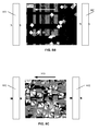
- Figure 2 is a simplified plan view of a ribbon formed by anisotropic magnetic flakes of the instant invention in an external magnetic field;
- Figure 3A is a perspective view of a substrate used for manufacturing anisotropic magnetic flakes of the instant invention.
- Figure 3B is a flow chart of a method of flake manufacturing in accordance with the instant invention.
- Figure 4A is an illustration of a magnetic material deposition according to one embodiment of the instant invention.
- Figure 4B is a plan view of the substrate shown in Fig. 4A ;
- Figure 5A is a side view illustration of a magnetic material deposition according to one embodiment of the instant invention.
- Figure 5B is a plan view of the substrate shown in Fig. 5A ;
- Figure 6A is a side view illustration of a magnetic material deposition according to one embodiment of the instant invention.
- Figure 6B is a plan view of the substrate shown in Fig. 6A ;
- Figure 7 is a side view illustration of a magnetic material deposition according to one embodiment of the instant invention.
- Figure 8A is a microscopic image of randomly aligned conventional flakes in absence of a magnetic field
- Figure 8B is a microscopic image of conventional flakes in a magnetic field
- Figure 8C is a microscopic image of anisotropic magnetic flakes of the instant invention in a magnetic field; concentration of the flakes in a carrier is 10wt%;
- Figure 8D is a microscopic image of anisotropic magnetic flakes of the instant invention forming ribbons in a magnetic field
- Figure 8E is a microscopic image of anisotropic magnetic flakes of the instant invention forming a highly reflective coating in a magnetic field;
- Figure 9A is a simplified plan view of shaped flakes
- Figure 9B is a simplified plan view of a ribbon formed by flakes of the instant invention with a hydrophobic coating
- Figure 9C is a simplified plan view of ribbons formed by flakes of the instant invention without a hydrophobic coating
- Figure 10 and 11 are simplified cross sections of flakes according to embodiments of the present invention.
- Figure 12 is a cross section of a magnetic flake with a reflective grating
- Figure 13 is a microphotograph of ribbon-like structures
- Figure 14 is an illustration of a method of object authentication.
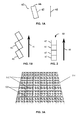
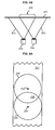
- a magnetic flake is a pigment flake that includes a magnetic material. It is known that a square-shaped magnetic flake without a diffraction grating has its easy magnetic axis, i.e. a direction of its magnetic moment, along a diagonal of the square, and North and South magnetic poles - at opposite corners of the square.
- Fig. 1A which is a copy of Fig. 2a from US Patent No. 7,300,695 issued November 27, 2007, to Argoitia et al. , illustrates a rectangular magnetic flake 40 with sides 42 and 44 in a liquid medium and under influence of a magnetic field. The flake 40 orients so as to have a diagonal along the direction of the applied magnetic field 46. North and South magnetic poles of different flakes attract and flakes may form corner-to-corner chains such as shown in Fig. 1B .
- the unexpected effect may be attributed to magnetic anisotropy caused by a method of flake manufacturing.
- Possible types of magnetic anisotropy such as magneto-crystalline anisotropy, stress-induced magnetic anisotropy, and magnetic anisotropy induced by the substrate topography, are described in " Hitchhiker's Guide to Magnetism,” Bruce M. Moskowitz, Environmental Magnetism Workshop, 5-8 June 1991 .
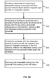
- the method of flake manufacturing includes a substrate-providing step 510 wherein a substrate is provided for supporting a releasable coating.
- a substrate embossing/etching step 520 the substrate, optionally with a coating thereon, is provided with a plurality of frames embossed or etched onto the substrate, for example as taught in US Patents No. 6,902,807 issued June 7, 2005 , and US Patent Application No. 20080107856 published May 8, 2008, both to Argoitia et al. and incorporated herein by reference.
- the shape and orientation of the frames is related to the direction of the anisotropy so that the two-dimensional shape of a frame has two sides substantially parallel to each other and substantially orthogonal to the desired anisotropy direction.
- a coating step 530 the substrate is coated with the releasable coating as disclosed in US Patents Nos. 6,838,166 issued January 4, 2005 , and 6,808,806 issued October 26, 2004, both to Phillips et al. and incorporated herein by reference.
- the releasable coating includes the first and second reflector layers and a magnetic layer formed of a magnetic material.
- the magnetic layer is deposited so as to have a magnetic anisotropy in a desired direction.
- a coating removing step 540 the releasable coating is removed from the substrate and broken apart providing anisotropic magnetic flakes of the instant invention.
- a substrate provided in the substrate-providing step 510 is patterned in the substrate embossing/etching step 520 following the step 510.
- a substrate 501 has a pattern of squares 502 separated by break-off trenches 503.
- the substrate 501 is made of polyester
- the squares 502 are squares of 20 x 20 micron with a logo "JDSU" impressed therein for the purpose of tracking orientation of the squares in a coating.
- the substrate 501 may have a different, not necessarily square, pattern of tranches 503, as it will be discussed further with reference to Figs. 9A-C .
- the releasable coating formed during the coating step 530 includes one or more magnetic layers and, optionally, non-magnetic layers as it will be discussed further with reference to Figs. 10 and 11 .
- the non-magnetic layers may be deposited using any conventional thin film deposition techniques. Non-limiting examples of such techniques include physical vapor deposition (PVD), chemical vapor deposition (CVD), plasma enhanced (PE) variations thereof, such as PECVD or downstream PECVD, sputtering, electrolytic deposition, sol-gel, and other like deposition methods that lead to the formation of substantially uniform continuous thin film layers. For deposition of the magnetic layer, these techniques are performed as described below.
- the coating step 530 includes deposition of the magnetic layer using at least two sources for providing magnetic material to a same portion of the substrate at different angles.
- the coating step 530 includes deposition of the magnetic layer using at least two sources for providing magnetic material to a same portion of a moving substrate simultaneously at two, or more, different angles.
- Figs. 4A and 4B schematically illustrate deposition of a magnetic material on the surface of a substrate 601 moving in a direction 602.
- the magnetic material is provided to the substrate 601 simultaneously from two magnetic material sources 603 and 604 disposed so that a line 610 connecting the magnetic material sources 603 and 604 is substantionally orthogonal to the direction 602.
- a charge of the magnetic material is placed into the magnetic material sources 603 and 604, or crucibles, and heated.
- the vapor of the magnetic material leaves the crucibles in two streams 605 and goes predominantly toward the substrate 601.
- the streams 605 intersect in a zone 606 within the vacuum chamber in close proximity to the substrate 601.
- the evaporant condenses on the cold substrate 601 producing a magnetic thin film layer 608 underneath the substrate 601.
- the two overlapping vapor streams 605 come to a portion of the substrate 601 simultaneously at two different angles.
- a magnetic layer of an individual flake has a microcrystalline or a domain structure providing a magnetic anisotropy oriented substantially parallel to one side of the square and orthogonal to another side of the square.
- the coating step 530 includes deposition of the magnetic layer illustrated in Figs. 5A and 5B . At least two sources of magnetic material are used for providing the magnetic material to a same portion of the substrate at different angles, wherein two or more sources of the magnetic material 103 and 104 are disposed along the direction 102 of the substrate's movement and oriented at different angles with respect to the substrate 101, so that two evaporation streams 105 reach a portion of the substrate 101 at different angles at different times.
- the coating step 530 includes deposition of the magnetic layer onto a static substrate as illustrated in Figs. 6A and 6B .
- Two or more sources of the magnetic material 203 and 204 create overlapping vapor streams 205 reaching the substrate 201 in a region 206 so as to provide magnetic material to a same portion of the substrate at two different angles.
- the substrate 201 shown in Figs. 6A and 6B can move.
- the substrate is moving during the deposition of magnetic layer in the coating step 530, preferably in the direction of the desired magnetic anisotropy.
- the coating step 530 includes deposition of the magnetic material onto a curved substrate as illustrated in Fig. 7 .
- the substrate 701 which is partially wrapped around a roller 702 inside of a roll-coater.
- a stream of the magnetic material 703 comes from a source of the magnetic material 704 such as an e-gun.
- a shield 705 prevents deposition of the material on the curved substrate 701 before it comes to the roller 702. Because of the substrate's curved surface, a same portion of the substrate 701 moving through the evaporated stream 703 receives the magnetic material at substantially different angles.
- a layer of the magnetic material deposited on the substrate 701 has a magnetic anisotropy oriented along the direction of the substrate's movement, since flakes made by removing a releasable coating from the substrate and breaking it apart exhibited side-by-side alignment when subjected to an external magnetic field.
- the method embodiment shown in Fig. 4A may use the substrate 601 bent as shown in Fig. 7 .
- the coating step 530 includes annealing of the magnetic material in a magnetic field for providing an anisotropy in a desired direction.
- the ion bombardment of the freshly deposited magnetic layer used for the same purpose.
- Xe-ion-irradiation of the magnetic material taught by Kun Zhang in "Stress induced magnetic anisotropy of Xe-ion-irradiated Ni thin films", Nucl. Instr. And Meth. In Phys. Res., B 243 (2006), 51-57 , incorporated herein by reference.
- the bombardment causes physical changes of the microstructure structure of the magnetic material producing strain.
- the method described herein with reference to Fig. 3B provides magnetic flakes having a predefined two-dimensional shape and a magnetic anisotropy oriented in a desired direction, which may be different from the direction of the longest planar dimension of the shape.
- Anisotropic magnetic flakes of the instant invention have a thickness in the range of 50 nm to 10 microns and a two-dimensional shape 900 having a diameter, i.e. a greatest distance between two points of the shape 900, in the range of 1 - 500 microns.
- the flakes manufactured using the aforedescribed method are non-diffractive, reflective, anisotropic, magnetic flakes for forming a reflective coating.
- the flakes have a particular shape and a magnetic anisotropy so as to enable forming ribbons when dispersed in a liquid carrier and impacted with an external magnetic field.
- the flakes include two reflector layers and a magnetic layer therebetween, and have a smooth surface absent of a grating, however indicia may be present.
- the flakes have a two-dimensional shape with two sides substantially parallel to one another, for example a square 930 has two parallel sides 938.
- the flakes are manufactured so as to have a magnetic anisotropy in a direction 936 substantially orthogonal to the two mutually parallel sides 938.
- a liquid carrier When such flakes are dispersed in a liquid carrier and impacted with an external magnetic field, they form ribbons such as shown in Fig. 2 .
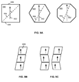
- the flakes have a square shape, but rectangles with unequal sides, parallelograms 900, hexagons 940, octagon 950, and any other shape having two sides substantially parallel to one another, are suitable for forming ribbons.
- the direction of the magnetic anisotropy 932, 942, or 952 forms with the longest planar dimension 934, 944, or 952, respectively, an angle of at least 20 degrees.
- flakes would require a hydrophobic coating for turning up the right surface of the flake as taught in US Application No: 12/051,164 filed March 19, 2008 , 241, incorporated herein by reference.
- parallelogram-shaped magnetic flakes 900 with a hydrophobic coating on one surface of the flake form better ordered ribbons shown in Fig. 9B than flakes without such a coating, as shown in Fig. 9C .
- the magnetic layer can be formed of any magnetic material, such as ferromagnetic and ferrimagnetic materials, including nickel, cobalt, iron, gadolinium, terbium, dysprosium, erbium, and their alloys or oxides.
- a cobalt nickel alloy can be employed, with the cobalt and nickel having a ratio by weight of about 80% and about 20%, respectively. This ratio for each of these metals in the cobalt nickel alloy can be varied by plus or minus about 10% and still achieve the desired results.
- cobalt can be present in the alloy in an amount from about 70% to about 90% by weight
- nickel can be present in the alloy in an amount from about 10% to about 30% by weight.
- alloys include Fe/Si, Fe/Ni, FeCo, Fe/Ni/Mo, and combinations thereof.
- Hard magnetics of the type SmCo5, NdCo5, Sm2Co17, Nd2Fel4B, Sr6Fe2O3, TbFe2, Al-Ni-Co, and combinations thereof, can also be used as well as spinel ferrites of the type Fe3O4, NiFe2O4, MnFe2O4, CoFe2O4, or garnets of the type YIG or GdIG, and combinations thereof.
- the magnetic material may be selected for its reflecting or absorbing properties as well as its magnetic properties. When utilized to function as a reflector, the magnetic material is deposited to a thickness so that it is substantially opaque. When utilized as an absorber, the magnetic material is deposited to a thickness so that it is not substantially opaque. A typical thickness for the magnetic material when utilized as an absorber is from about 2 nm to about 20 nm.
- the magnetic layer may be formed by a material having magnetic and non-magnetic particles, or magnetic particle within non-magnetic medium, for example cobalt-doped zinc oxide film deposited using the sol-gel technology.
- the term “hard magnets” also called permanent magnets
- a ferromagnetic material is any material that has a permeability substantially greater than 1 and that exhibits magnetic hysteresis properties.
- the magnetic materials used to form magnetic layers in the flakes and foils of the invention have a coercivity of less than about 2000 Oe, more preferably less than about 300 Oe.
- Coercivity refers to the ability of a material to be demagnetized by an external magnetic field. The higher the value of coercivity, the higher the magnetic field required to de-magnetize the material after the field is removed.
- the magnetic layers used are preferably "soft" magnetic materials (easily demagnetized), as opposed to "hard” magnetic materials (difficult to demagnetize) which have higher coercivities.
- the coercivities of the foils, pigments or colorants of the magnetic color shifting designs according to the invention are preferably in a range of about 50 Oe to about 300 Oe. These coercivities are lower than in standard recording materials.
- the use of soft magnetic materials in pigment flakes allows for easier dispersion of the flakes without clumping.
- the magnetic layer can be formed to have a suitable physical thickness of from about 200 angstroms to about 10,000 angstroms, and preferably from about 500 to about 1,500 angstroms.
- a suitable physical thickness of from about 200 angstroms to about 10,000 angstroms, and preferably from about 500 to about 1,500 angstroms.
- the optimal magnetic thickness will vary depending on the particular magnetic material used and the purpose for its use.
- Anisotropic magnetic flakes have one or more substantially continuous thin-film layers, including a magnetic layer having a magnetic anisotropy oriented as discussed above.
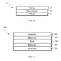
- the anisotropic reflective magnetic flakes (RMF) 20 include two reflector layers 24 and 26 on both major surfaces of a magnetic layer 22 having anisotropy as discussed above.
- the reflector layers 24 and 26 can be composed of various reflective materials. Presently preferred materials are one or more metals, one or more metal alloys, or combinations thereof, because of their high reflectivity and ease of use, although non-metallic reflective materials could also be used.
- Nonlimiting examples of suitable metallic materials for the reflector layers include aluminum, silver, copper, gold, platinum, tin, titanium, palladium, nickel, cobalt, rhodium, niobium, chromium, and combinations or alloys thereof.
- the reflector layers can be formed to have a suitable physical thickness of from about 40 to about 2,000 nm, and preferably from about 60 to about 1,000 nm.
- the reflector layers have a reflectivity of at least 40 % and preferably higher than 60 %.
- the anisotropic reflective magnetic flakes include two protective layers disposed on the reflector layers, not shown in Fig. 10 ;
- the protective layers are dielectric layers formed of such materials as zinc sulfide (ZnS), zinc oxide (ZnO), zirconium oxide (ZrO2), titanium dioxide (TiO2), diamond-like carbon, indium oxide (In203), indium-tin-oxide (ITO), tantalum pentoxide (Ta2O5), ceric oxide (CeO2) yttrium oxide (Y2O3), europium oxide (Eu2O3), iron oxides such as (II)diiron(III) oxide (Fe3O4) and ferric oxide (Fe2O3 hafnium nitride (HfN), hafnium carbide (HfC), hafnium oxide (HfO2) lanthanum oxide (La2O3), magnesium oxide (MgO), neodymium oxide (Nd2O3), praseodym
- the anisotropic reflective magnetic flakes of the instant invention are color-shifting flakes 300 shown in Fig. 11 , including an RMF 342 formed of a magnetic layer and two reflector layers on two surfaces of the magnetic layer, two dielectric layers 344 and 346 supported by the reflector layers of the RMF 342, and two absorber layers 348 and 350 supported by the dielectric layers 344 and 346, for providing a color-shifting optical effect.
- Materials suitable for the magnetic, reflector and dielectric layers are the same as listed above with reference to Fig.10 .
- the coatings formed using the color-shifting flakes 300 are highly-reflective, color-shifting coatings with ribbons formed therein.
- Nonlimiting examples of suitable absorber materials include metallic absorbers such as chromium, aluminum, nickel, silver, copper, palladium, platinum, titanium, vanadium, cobalt, iron, tin, tungsten, molybdenum, rhodium, and niobium, as well as their corresponding oxides, sulfides, and carbides.
- Other suitable absorber materials include carbon, graphite, silicon, germanium, cermet, ferric oxide or other metal oxides, metals mixed in a dielectric matrix, and other substances that are capable of acting as a uniform or selective absorber in the visible spectrum.
- Various combinations, mixtures, compounds, or alloys of the above absorber materials may be used to form the absorber layers of flake 300.
- suitable alloys of the above absorber materials include Inconel (NiCr-Fe), stainless steels, Hastalloys (e.g., Ni-Mo-Fe; Ni-Mo-Fe-Cr; Ni-Si-Cu) and titanium-based alloys, such as titanium mixed with carbon (Ti/C), titanium mixed with tungsten (Ti/W), titanium mixed with niobium (Ti/Nb), and titanium mixed with silicon (Ti/Si), and combinations thereof.
- the absorber layers can also be composed of an absorbing metal oxide, metal sulfide, metal carbide, or combinations thereof.
- one preferred absorbing sulfide material is silver sulfide.
- suitable compounds for the absorber layers include titanium-based compounds such as titanium nitride (TiN), titanium oxynitride (TiNxOy), titanium carbide (TiC), titanium nitride carbide (TiNxCz), titanium oxynitride carbide (TiNxOyCz), titanium silicide (TiSi2), titanium boride (TiB2), and combinations thereof
- the absorber layers can be composed of a titanium-based alloy disposed in a matrix of Ti, or can be composed of Ti disposed in a matrix of a titanium-based alloy.
- a ribbon-forming anisotropic magnetic flake has a magnetic layer, by way of example, formed of nickel, having a shape and anisotropy as discussed above, which does not support any reflector layers.
- the reflector layers are desirable for providing a higher reflectivity of the coating.
- a web substrate patterned as shown in Fig. 3 was coated with a releasable thin-film coating MgF 2 /Al/Ni/Al/MgF 2 in a batch coater.
- the deposited coating was stripped off the substrate and ground until all particles were broken along break-off trenches 503.
- the resulting flakes were mixed with transparent UV-curable ink vehicle in concentration of 20wt% to produce a magnetic pigment.
- the ink was screen-printed on a paper card and cured in UV light.
- a microscopic image in Fig. 8A illustrates a random alignment of the flakes. Additionally.
- flakes of the same type were mixed with the ink vehicle in a smaller concentration (2wt%), printed onto another paper card and inserted between two permanent magnets 801 and 802 as illustrated in Fig. 8B , wherein the flakes aligned to have their diagonals substantially along the field direction 803.
- Non-grated, anisotropic, reflective, magnetic flakes were manufactured using a method of the instant invention illustrated in Figs. 4A and 4B , wherein the substrate 601 was arched in a roll coater as shown in Fig. 7 .
- a releasable coating MgF 2 /Al/Ni/Al/MgF 2 have been deposited on the substrate, then stripped off the substrate and ground until all platelets were broken into squares.
- the resulting flakes were mixed with the same ink vehicle in the concentration of 10wt% and printed on a paper card.
- a wet print containing magnetic flakes was placed between two magnets 801 and 802. The direction of an applied magnetic field is indicated by the arrow 803.
- the flakes in accordance with the instant invention manufactured to have a magnetic moment in the direction of one side of the square, aligned with their sides parallel to the direction of applied magnetic field 803.
- An increase of the flake concentration allows their assembly in long ribbon shown in Fig. 8D .
- a further increase of concentration brings the flakes close to each other ( Fig. 8E ) forming a highly reflective coating on a paper card.
- the non-grated, anisotropic, reflective, magnetic flakes of the instant invention are designed for forming a highly reflective coating, in particular desirable in the printing industry.
- a conventional method of increasing reflectivity of a metallic pigment includes surface modification of a metal flake by surfactants, such as fatty acids.
- the surfactants reduce the surface energy of the flake and make it float to the surface of the coating.
- the surfactants substantially reduce the abrasion wear of the coating.
- the coating provides a color-shifting effect if the flakes are color-shifting anisotropic reflective magnetic flakes.
- the reflective flakes have a substantially smooth surface for providing high specular reflectivity of the coating.
- the flakes have no grating, but may have indicia thereon.
- a carrier and a plurality of flakes dispersed therein are provided to a surface of an object and then a magnetic field is applied for orientation of the flakes parallel to the surface of the coating.
- Carriers are typically liquid for a period to permit some motion of the flake before the carrier evaporates or hardens.
- ink might have a volatile carrier that evaporates to fix the flake, or a clear paint carrier, such as a clear paint base, might harden to fix the flake.
- a clear paint carrier such as a clear paint base
- uncured thermosetting resin or heated thermoplastic resin might allow the flake to be oriented prior to curing or cooling, respectively, either before, during, or after application to a surface.
- the carrier is an acrylic resin based carrier; other carriers are readily known to one skilled in the art.
- Examples of carriers include polyvinyl alcohol, polyvinyl acetate polyvinylpyrrolidone, poly(ethoxyethylene), poly(methoxyethylene), poly(acrylic) acid, poly(acrylamide), poly(oxyethylene), poly(maleic anhydride), hydroxyethyl cellulose, cellulose acetate, poly(sacchrides) such as gum arabic and pectin, poly(acetals) such as polyvinylbutyral, poly(vinyl halides) such as polyvinyl chloride and polyvinylene chloride, poly(dienes) such as polybutadiene, poly(alkenes) such as polyethylene, poly(acrylates) such as polymethyl acrylate, poly(methacrylates) such as poly methylmethacrylate, poly(carbonates) such as poly(oxycarbonyl oxyhexamethylene, poly(esters) such as polyethylene terephthalate, poly(urethanes), poly(siloxanes), poly(suphides), poly
- the flakes have reflector layers having reflectivity of greater than 50% and, preferably, greater than 60%, and the flakes have a specific shape and magnetic anisotropy for tiling a surface of the coated object with flakes adjacent to one another substantionally leaving no surface open, provided a concentration of the flakes is high enough.
- the ribbons are understood to have at least three flakes adjacent side-by-side with gaps between the flakes of no greater than 500 nm. No gaps were noticed for the flakes in the size range of 1-20 microns. When the flakes have a size in the range of 20-500 microns, the gap size varies from zero to 500 nm. Of course, formation of the ribbons depends on a concentration of the flakes in the carrier.
- an aggregate surface of the flakes i.e. a sum of all flake surfaces turned to an observer, is equal to at least 80% of the surface's area under the coating.
- the aggregate surface of the flakes is greater than 90 % of the surface's area under the coating.
- concentration of the flakes provides substantially total coverage of the object's surface with ribbons of the flakes forming substantially a tile array of flakes shown in Fig. 8E .
- the tile array is understood as including at least two ribbons adjacent to one another so as to be side-by-side with gaps between the ribbons of no greater than 4 microns.
- the flakes of the instant invention provide a thin, cost-effective, highly-reflective coating.
- flakes aligned in a ribbon provide a security feature to the object with no extra cost or effort.
- the ribbons can be used for authentication of the object.
- a conventional image recognition technique applied to the image reflected by the coating so as to indentify whether any ribbons are present therein.
- anisotropic, reflective, magnetic flakes with a non-periodic linear grating are dispersed in a carrier for forming a coating with well-defined ribbons, which may be used as a security feature.
- the flakes with a non-periodic linear grating have the same layered structure and two-dimensional shape as the non-diffractive, anisotropic, reflective, magnetic flakes described above.
- the flakes of this embodiment may be reflective or a color-shifting, they have a non-symmetric and non-periodic structure of the grating that reduces presence of diffractive colors.
- a grating is any regularly spaced collection of essentially identical, parallel, elongated elements. In some instances, the grating can be non-periodic non-regularly spaced collection of non-identical parallel elongated elements.
- Gratings can be diffractive, holographic, reflective, binary, etc.
- a grating can also be a picture having characteristics of a grating. Holographic gratings are widely used for fabrication of holograms in packaging industry, for security applications and in the art. Diffractive gratings are also used for packaging. Diffractive flakes are fabricated by deposition of an optical stack onto a surface of a substrate with a diffractive grating. These flakes provide diffractive colors when illuminated by light.
- Magnetic diffractive flakes orient themselves with their grating parallel to the direction of applied magnetic field. Being dispersed in ink and aligned in the magnetic field, the shapeless diffractive flakes of different sizes form chains similar to one shown in Fig. 1B .
- Magnetic flakes with reflective gratings are illustrated in Fig. 12 .
- the widths of the elements of the grating are not equal to each other: W 1 ⁇ W 2 ⁇ W 3 ⁇ W 4 ⁇ W 5 as well as their heights: H 1 ⁇ H 2 ⁇ H 3 .
- a single pigment flake needs just a few (usually from one to four) grooves to provide flake orientation in the field.
- the size of the flake can be in the range of 2x 2 microns to 200 x 200 microns.
- the heights H ( Fig. 12 ) of the grating elements can be in the range of 10 nm to 100nm.
- the widths of the grating elements can be in the range of 10nm to 90nm.
- Rectangular magnetic reflective grating flakes all having a same shape, being dispersed in an ink vehicle and exposed to an external magnetic field, orient themselves along the direction of the field and assemble in long ribbon-like structures of an equal width as shown in Fig. 13 .
- the direction of the magnetic anisotropy is the direction of the non-periodic grating. Therefore, for forming ribbons in a coating, the anisotropic, reflective, magnetic flakes with a non-periodic grating have a two-dimensional shape with two sides substantially parallel to each other, and a non-periodic grating substantially orthogonal to the two sides.
- a thin film composition MgF 2 /Al/Ni/Al/ MgF 2 was deposited on the top of structured substrate having embossed patterns of 20 x 20 micron squares. Every square consisted of four flat embossed elements (hills) and three narrow debossed (valleys) elements. The widths of the embossed and debossed elements were different to reduce the diffractive component of the light reflected from the flake.
- the coated structure was released from the substrate and ground.
- the flakes were mixed with a transparent ink vehicle 470, silk screen printed on a transparent polyester card and exposed to the parallel magnetic field..
- the ink composition was solidified with UV lamp and microscopically analyzed. As shown in Fig. 13 , square magnetic reflective flakes 480 form continuous, well-defined ribbons of constant width, often extending from one side of the printed coating to another.
- Fig. 14 illustrates a method of authentication of an object such as a bank note 430, which has a printed coating 420.
- the coating 420 includes diffractive, anisotropic, reflective, magnetic flakes with a binary (fanout) grating disclosed in US Application No. 12/107,152 filed April 22, 2008 , incorporated herein by reference.
- the flakes are coated with an oleophobic/hydrophobic material so as to be aligned on the surface of the ink.
- a monochromatic beam of light 410 from a laser 400 illuminates the printed coating 420 containing ribbons.
- Reflected beams 440, forming a predetermined pattern are received at an image sensor or CCD camera 450 connected to a computer 460 or a reader.
- the computer 460 decodes the pattern so as to authenticate the bank note 430.
Landscapes
- Chemical & Material Sciences (AREA)
- Engineering & Computer Science (AREA)
- Organic Chemistry (AREA)
- Materials Engineering (AREA)
- Life Sciences & Earth Sciences (AREA)
- Wood Science & Technology (AREA)
- Nanotechnology (AREA)
- Power Engineering (AREA)
- Crystallography & Structural Chemistry (AREA)
- Business, Economics & Management (AREA)
- Accounting & Taxation (AREA)
- Finance (AREA)
- Physics & Mathematics (AREA)
- Composite Materials (AREA)
- Condensed Matter Physics & Semiconductors (AREA)
- General Physics & Mathematics (AREA)
- Inorganic Chemistry (AREA)
- General Chemical & Material Sciences (AREA)
- Chemical Kinetics & Catalysis (AREA)
- Pigments, Carbon Blacks, Or Wood Stains (AREA)
- Application Of Or Painting With Fluid Materials (AREA)
- Magnetic Record Carriers (AREA)
- Paints Or Removers (AREA)
- Credit Cards Or The Like (AREA)
- Soft Magnetic Materials (AREA)
- Manufacturing Of Magnetic Record Carriers (AREA)
- Laminated Bodies (AREA)
Abstract
Description
- The present invention relates generally to thin pigment flakes, and more particularly to providing alignment of thin magnetic flakes in an external magnetic field.
- Reflective metallic and color-shifting flakes are used in reflective and color-shifting inks or paints. Images printed with the inks or coatings made using the paints have their reflective or color parameters worse than those of a solitary flake due to the gaps between adjacent flakes filled with a less reflective carrier. An increase of pigment concentration can improve the reflectivity of the printed images and paint coatings, but is associated with additional cost, with thicker coatings, and with flakes overlapping one another preventing them from lying flat against the substrate.
- Accordingly, it is an object of the instant invention to provide a cost effective highly reflective coating containing reflective or color-shifting flakes. It is another object of the invention to provide flakes for such coatings or inks, as well as a method of manufacturing the flakes enabling said coatings. It is yet another object of the invention to provide a method of authentication of an object having the reflective coating thereon.
- The present invention relates to an anisotropic magnetic flake for forming a reflective coating. The flake has a layered structure having a thickness in the range of 50 nm - 10 microns and a two-dimensional shape with a longest planar dimension in the range of 1 - 500 microns. The layered structure includes first and second reflector layers having reflectivity of greater than 50%, for providing reflectivity to the reflective coating, and a magnetic layer between the first and second reflector layers, for aligning the flake substantially parallel to the surface of the reflective coating, when said flake is disposed in a liquid carrier under influence of an external magnetic field. The magnetic layer has a structure which provides in-plane magnetic anisotropy forming an angle of at least 20 degrees with the longest planar dimension.
- One aspect of the invention relates to the described above flakes having a specific two-dimensional shape particularly well suited for making ribbons. The shape of the flakes has two sides substantially parallel to each other. The magnetic layer is formed so as to have an in-plane magnetic anisotropy substantially orthogonal to the two sides for alignment of the flake side-by-side with one or more flakes of a same structure when said flakes are disposed in a liquid carrier under influence of an external magnetic field while forming the reflective coating. The flakes have no grating thereon for providing high specular reflectivity. Preferably, the flakes have a square shape.
- Another aspect of the present invention relates to a method of manufacturing the flakes wherein the anisotropy of the magnetic layer is substantially orthogonal to two sides of the two-dimensional shape of the flake. The method includes the steps of: (a) providing a substrate for supporting a releasable coating including the first and second reflector layers and the magnetic layer formed of a magnetic material; (b) embossing or etching the substrate with a plurality of frames having the two-dimensional shape with the two sides substantially orthogonal to a first direction, before or after the releasable coating is applied to the substrate; (c) coating the substrate with the releasable coating so as to provide the magnetic layer having a magnetic anisotropy in the first direction, wherein the releasable coating upon removal from the substrate breaks apart into the flakes; and, (d) removing the releasable coating from the substrate and breaking it into the flakes. In one embodiment of the method, the magnetic layer is deposited using two sources which provide the magnetic material to a same portion of the substrate from different angles.
- Yet another aspect of the present invention relates to a coating including a solidified carrier and a plurality of flakes dispersed therein. All the flakes have a same two-dimensional shape, such that two sides thereof are substantially parallel to each other, and have the magnetic layer such that the in-plane magnetic anisotropy is substantially orthogonal to said two sides. A portion of the flakes forms a ribbon of at least three flakes adjacent to one another so as to be side-by-side with gaps between the flakes of no greater than 500 nm, when said flakes are disposed in a liquid carrier under influence of an external magnetic field while forming the coating.
- The ribbons of three or more flakes may be used as a security feature on documents, banknotes, etc. The instant invention provides a method of authentication of an object including the step of identifying a ribbon in a flake-containing coating. In one embodiment, the flakes forming the ribbon have a binary grating thereon, which provides a pattern of reflected light beams used for authentication of the object.
- The invention will be described in greater detail with reference to the accompanying drawings which represent preferred embodiments thereof wherein:
-
Figure 1A is a simplified plan view of a conventional magnetic flake in an external magnetic field, according to prior art; -
Figure 1B is a simplified plan view of a chain formed of magnetic flakes shown inFig. 1A , in an external magnetic field; -
Figure 2 is a simplified plan view of a ribbon formed by anisotropic magnetic flakes of the instant invention in an external magnetic field; -
Figure 3A is a perspective view of a substrate used for manufacturing anisotropic magnetic flakes of the instant invention; -
Figure 3B is a flow chart of a method of flake manufacturing in accordance with the instant invention; -
Figure 4A is an illustration of a magnetic material deposition according to one embodiment of the instant invention; -
Figure 4B is a plan view of the substrate shown inFig. 4A ; -
Figure 5A is a side view illustration of a magnetic material deposition according to one embodiment of the instant invention; -
Figure 5B is a plan view of the substrate shown inFig. 5A ; -
Figure 6A is a side view illustration of a magnetic material deposition according to one embodiment of the instant invention; -
Figure 6B is a plan view of the substrate shown inFig. 6A ; -
Figure 7 is a side view illustration of a magnetic material deposition according to one embodiment of the instant invention; -
Figure 8A is a microscopic image of randomly aligned conventional flakes in absence of a magnetic field; -
Figure 8B is a microscopic image of conventional flakes in a magnetic field; -
Figure 8C is a microscopic image of anisotropic magnetic flakes of the instant invention in a magnetic field; concentration of the flakes in a carrier is 10wt%; -
Figure 8D is a microscopic image of anisotropic magnetic flakes of the instant invention forming ribbons in a magnetic field; -
Figure 8E is a microscopic image of anisotropic magnetic flakes of the instant invention forming a highly reflective coating in a magnetic field; -
Figure 9A is a simplified plan view of shaped flakes; -
Figure 9B is a simplified plan view of a ribbon formed by flakes of the instant invention with a hydrophobic coating; -
Figure 9C is a simplified plan view of ribbons formed by flakes of the instant invention without a hydrophobic coating; -
Figure 10 and 11 are simplified cross sections of flakes according to embodiments of the present invention; -
Figure 12 is a cross section of a magnetic flake with a reflective grating; -
Figure 13 is a microphotograph of ribbon-like structures; and -
Figure 14 is an illustration of a method of object authentication. - A magnetic flake is a pigment flake that includes a magnetic material. It is known that a square-shaped magnetic flake without a diffraction grating has its easy magnetic axis, i.e. a direction of its magnetic moment, along a diagonal of the square, and North and South magnetic poles - at opposite corners of the square.
Fig. 1A , which is a copy of Fig. 2a fromUS Patent No. 7,300,695 issued November 27, 2007, to Argoitia et al. , illustrates a rectangularmagnetic flake 40 withsides flake 40 orients so as to have a diagonal along the direction of the appliedmagnetic field 46. North and South magnetic poles of different flakes attract and flakes may form corner-to-corner chains such as shown inFig. 1B . - It has been unexpectedly discovered that, when dispersed in a liquid carrier and impacted by a magnetic field, square-shaped, non-grated magnetic flakes of a particular kind form different structures, namely ribbons. With reference to
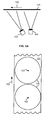
Fig. 2 flakes 47 within theribbons 48 are adjacent to each other side-by-side as opposite to the corner-to-corner adjacency shown inFig. 1B . The side-by-side attraction of twoflakes 47 manifests the location of magnetic poles at two opposite sides of thesquare flake 47 and the direction of a magnetic moment parallel to two other sides of the square 47. Thesquare flakes 47 orient in amagnetic field 46 so as to align a side of aflake 47 along the lines of themagnetic field 46. - In general terms, conventional non-diffractive flakes have easy axes along their longest planar dimensions, whereas the flake of the instant invention has an easy axis, or magnetic anisotropy, at an angle with the longest planar dimension.
- The unexpected effect may be attributed to magnetic anisotropy caused by a method of flake manufacturing. Possible types of magnetic anisotropy, such as magneto-crystalline anisotropy, stress-induced magnetic anisotropy, and magnetic anisotropy induced by the substrate topography, are described in "Hitchhiker's Guide to Magnetism," Bruce M. Moskowitz, Environmental Magnetism Workshop, 5-8 June 1991.
- With reference to
Fig. 3B , the method of flake manufacturing includes a substrate-providingstep 510 wherein a substrate is provided for supporting a releasable coating. In a substrate embossing/etching step 520, the substrate, optionally with a coating thereon, is provided with a plurality of frames embossed or etched onto the substrate, for example as taught inUS Patents No. 6,902,807 issued June 7, 2005 , andUS Patent Application No. 20080107856 published May 8, 2008, both to Argoitia et al. and incorporated herein by reference. The shape and orientation of the frames is related to the direction of the anisotropy so that the two-dimensional shape of a frame has two sides substantially parallel to each other and substantially orthogonal to the desired anisotropy direction. - Then, in a
coating step 530, the substrate is coated with the releasable coating as disclosed inUS Patents Nos. 6,838,166 issued January 4, 2005 , and6,808,806 issued October 26, 2004, both to Phillips et al. and incorporated herein by reference. The releasable coating includes the first and second reflector layers and a magnetic layer formed of a magnetic material. The magnetic layer is deposited so as to have a magnetic anisotropy in a desired direction. Then, in acoating removing step 540, the releasable coating is removed from the substrate and broken apart providing anisotropic magnetic flakes of the instant invention. - In one embodiment of the method, a substrate provided in the substrate-providing
step 510 is patterned in the substrate embossing/etching step 520 following thestep 510. With reference to inFig. 3A , asubstrate 501 has a pattern ofsquares 502 separated by break-offtrenches 503. By way of example, thesubstrate 501 is made of polyester, thesquares 502 are squares of 20 x 20 micron with a logo "JDSU" impressed therein for the purpose of tracking orientation of the squares in a coating. Thesubstrate 501 may have a different, not necessarily square, pattern oftranches 503, as it will be discussed further with reference toFigs. 9A-C . - The releasable coating formed during the
coating step 530 includes one or more magnetic layers and, optionally, non-magnetic layers as it will be discussed further with reference toFigs. 10 and 11 . The non-magnetic layers may be deposited using any conventional thin film deposition techniques. Non-limiting examples of such techniques include physical vapor deposition (PVD), chemical vapor deposition (CVD), plasma enhanced (PE) variations thereof, such as PECVD or downstream PECVD, sputtering, electrolytic deposition, sol-gel, and other like deposition methods that lead to the formation of substantially uniform continuous thin film layers. For deposition of the magnetic layer, these techniques are performed as described below. - In one embodiment of the method, the
coating step 530 includes deposition of the magnetic layer using at least two sources for providing magnetic material to a same portion of the substrate at different angles. - By way of example, in one embodiment of the method, the
coating step 530 includes deposition of the magnetic layer using at least two sources for providing magnetic material to a same portion of a moving substrate simultaneously at two, or more, different angles.Figs. 4A and 4B schematically illustrate deposition of a magnetic material on the surface of asubstrate 601 moving in adirection 602. The magnetic material is provided to thesubstrate 601 simultaneously from twomagnetic material sources line 610 connecting themagnetic material sources direction 602. A charge of the magnetic material is placed into themagnetic material sources streams 605 and goes predominantly toward thesubstrate 601. Thestreams 605 intersect in azone 606 within the vacuum chamber in close proximity to thesubstrate 601. The evaporant condenses on thecold substrate 601 producing a magneticthin film layer 608 underneath thesubstrate 601. The two overlappingvapor streams 605 come to a portion of thesubstrate 601 simultaneously at two different angles. It is our understanding that they provide nucleation and growth of the magnetic material creating a microcrystalline structure of grains of the condensate such that themagnetic layer 608 acquires an in-plane magnetic anisotropy in thedirection 602 orthogonal to the line connecting theevaporation sources magnetic layer 608 is then stripped off thesubstrate 601 and ground-broken along thetrenches 503 shown inFig. 3A into individual square-shaped flakes. As a result, a magnetic layer of an individual flake has a microcrystalline or a domain structure providing a magnetic anisotropy oriented substantially parallel to one side of the square and orthogonal to another side of the square. - In one embodiment of the method, the
coating step 530 includes deposition of the magnetic layer illustrated inFigs. 5A and5B . At least two sources of magnetic material are used for providing the magnetic material to a same portion of the substrate at different angles, wherein two or more sources of themagnetic material direction 102 of the substrate's movement and oriented at different angles with respect to thesubstrate 101, so that twoevaporation streams 105 reach a portion of thesubstrate 101 at different angles at different times. - In one embodiment of the method, the
coating step 530 includes deposition of the magnetic layer onto a static substrate as illustrated inFigs. 6A and6B . Two or more sources of themagnetic material vapor streams 205 reaching thesubstrate 201 in aregion 206 so as to provide magnetic material to a same portion of the substrate at two different angles. Alternatively, thesubstrate 201 shown inFigs. 6A and6B can move. - In one embodiment of the method, the substrate is moving during the deposition of magnetic layer in the
coating step 530, preferably in the direction of the desired magnetic anisotropy. - In one embodiment of the method, the
coating step 530 includes deposition of the magnetic material onto a curved substrate as illustrated inFig. 7 . Thesubstrate 701, which is partially wrapped around aroller 702 inside of a roll-coater. A stream of themagnetic material 703 comes from a source of themagnetic material 704 such as an e-gun. Ashield 705 prevents deposition of the material on thecurved substrate 701 before it comes to theroller 702. Because of the substrate's curved surface, a same portion of thesubstrate 701 moving through the evaporatedstream 703 receives the magnetic material at substantially different angles. It has been proven experimentally, that a layer of the magnetic material deposited on thesubstrate 701 has a magnetic anisotropy oriented along the direction of the substrate's movement, since flakes made by removing a releasable coating from the substrate and breaking it apart exhibited side-by-side alignment when subjected to an external magnetic field. - Of course, features of different embodiments described herein can be combined. By way of example, the method embodiment shown in
Fig. 4A may use thesubstrate 601 bent as shown inFig. 7 . - In one embodiment of the method, the
coating step 530 includes annealing of the magnetic material in a magnetic field for providing an anisotropy in a desired direction. In another embodiment, the ion bombardment of the freshly deposited magnetic layer used for the same purpose. By way of example, Xe-ion-irradiation of the magnetic material taught by Kun Zhang in "Stress induced magnetic anisotropy of Xe-ion-irradiated Ni thin films", Nucl. Instr. And Meth. In Phys. Res., B 243 (2006), 51-57, incorporated herein by reference. The bombardment causes physical changes of the microstructure structure of the magnetic material producing strain. - The method described herein with reference to
Fig. 3B provides magnetic flakes having a predefined two-dimensional shape and a magnetic anisotropy oriented in a desired direction, which may be different from the direction of the longest planar dimension of the shape. Anisotropic magnetic flakes of the instant invention have a thickness in the range of 50 nm to 10 microns and a two-dimensional shape 900 having a diameter, i.e. a greatest distance between two points of theshape 900, in the range of 1 - 500 microns. - In one embodiment of the instant invention, the flakes manufactured using the aforedescribed method are non-diffractive, reflective, anisotropic, magnetic flakes for forming a reflective coating. The flakes have a particular shape and a magnetic anisotropy so as to enable forming ribbons when dispersed in a liquid carrier and impacted with an external magnetic field. The flakes include two reflector layers and a magnetic layer therebetween, and have a smooth surface absent of a grating, however indicia may be present.
- With reference to
Figs 9A-C , the flakes have a two-dimensional shape with two sides substantially parallel to one another, for example a square 930 has twoparallel sides 938. The flakes are manufactured so as to have a magnetic anisotropy in a direction 936 substantially orthogonal to the two mutuallyparallel sides 938. When such flakes are dispersed in a liquid carrier and impacted with an external magnetic field, they form ribbons such as shown inFig. 2 . - Preferably, the flakes have a square shape, but rectangles with unequal sides,
parallelograms 900,hexagons 940,octagon 950, and any other shape having two sides substantially parallel to one another, are suitable for forming ribbons. The direction of themagnetic anisotropy planar dimension - Depending on the two-dimensional shape, some flakes would require a hydrophobic coating for turning up the right surface of the flake as taught in
US Application No: 12/051,164 filed March 19, 2008 magnetic flakes 900 with a hydrophobic coating on one surface of the flake form better ordered ribbons shown inFig. 9B than flakes without such a coating, as shown inFig. 9C . - The magnetic layer can be formed of any magnetic material, such as ferromagnetic and ferrimagnetic materials, including nickel, cobalt, iron, gadolinium, terbium, dysprosium, erbium, and their alloys or oxides. For example, a cobalt nickel alloy can be employed, with the cobalt and nickel having a ratio by weight of about 80% and about 20%, respectively. This ratio for each of these metals in the cobalt nickel alloy can be varied by plus or minus about 10% and still achieve the desired results. Thus, cobalt can be present in the alloy in an amount from about 70% to about 90% by weight, and nickel can be present in the alloy in an amount from about 10% to about 30% by weight. Other examples of alloys include Fe/Si, Fe/Ni, FeCo, Fe/Ni/Mo, and combinations thereof. Hard magnetics of the type SmCo5, NdCo5, Sm2Co17, Nd2Fel4B, Sr6Fe2O3, TbFe2, Al-Ni-Co, and combinations thereof, can also be used as well as spinel ferrites of the type Fe3O4, NiFe2O4, MnFe2O4, CoFe2O4, or garnets of the type YIG or GdIG, and combinations thereof. The magnetic material may be selected for its reflecting or absorbing properties as well as its magnetic properties. When utilized to function as a reflector, the magnetic material is deposited to a thickness so that it is substantially opaque. When utilized as an absorber, the magnetic material is deposited to a thickness so that it is not substantially opaque. A typical thickness for the magnetic material when utilized as an absorber is from about 2 nm to about 20 nm.
- The magnetic layer may be formed by a material having magnetic and non-magnetic particles, or magnetic particle within non-magnetic medium, for example cobalt-doped zinc oxide film deposited using the sol-gel technology.
- Although this broad range of magnetic materials can be used, the "soft" magnets are preferred. As used herein, the term "soft magnets" refers to any material exhibiting ferromagnetic properties but having a remanence that is substantially zero after exposure to a magnetic force. Soft magnets show a quick response to an applied magnetic field, but have very low (coercive fields (Hc)=0.05-300 Oersteds (Oe)) or zero magnetic signatures, or retain very low magnetic lines of force after the magnetic field is removed. Similarly, as used herein, the term "hard magnets" (also called permanent magnets) refers to any material that exhibits ferromagnetic properties and that has a long lasting remanence after exposure to a magnetizing force. A ferromagnetic material is any material that has a permeability substantially greater than 1 and that exhibits magnetic hysteresis properties.
- Preferably, the magnetic materials used to form magnetic layers in the flakes and foils of the invention have a coercivity of less than about 2000 Oe, more preferably less than about 300 Oe. Coercivity refers to the ability of a material to be demagnetized by an external magnetic field. The higher the value of coercivity, the higher the magnetic field required to de-magnetize the material after the field is removed. The magnetic layers used are preferably "soft" magnetic materials (easily demagnetized), as opposed to "hard" magnetic materials (difficult to demagnetize) which have higher coercivities. The coercivities of the foils, pigments or colorants of the magnetic color shifting designs according to the invention are preferably in a range of about 50 Oe to about 300 Oe. These coercivities are lower than in standard recording materials. The use of soft magnetic materials in pigment flakes allows for easier dispersion of the flakes without clumping.
- The magnetic layer can be formed to have a suitable physical thickness of from about 200 angstroms to about 10,000 angstroms, and preferably from about 500 to about 1,500 angstroms. However, it will be appreciated by those skilled in the art, in view of the disclosure herein, that the optimal magnetic thickness will vary depending on the particular magnetic material used and the purpose for its use.
- Anisotropic magnetic flakes have one or more substantially continuous thin-film layers, including a magnetic layer having a magnetic anisotropy oriented as discussed above. With reference to
Fig. 10 , the anisotropic reflective magnetic flakes (RMF) 20 include tworeflector layers - Optionally, the anisotropic reflective magnetic flakes include two protective layers disposed on the reflector layers, not shown in
Fig. 10 ; the protective layers are dielectric layers formed of such materials as zinc sulfide (ZnS), zinc oxide (ZnO), zirconium oxide (ZrO2), titanium dioxide (TiO2), diamond-like carbon, indium oxide (In203), indium-tin-oxide (ITO), tantalum pentoxide (Ta2O5), ceric oxide (CeO2) yttrium oxide (Y2O3), europium oxide (Eu2O3), iron oxides such as (II)diiron(III) oxide (Fe3O4) and ferric oxide (Fe2O3 hafnium nitride (HfN), hafnium carbide (HfC), hafnium oxide (HfO2) lanthanum oxide (La2O3), magnesium oxide (MgO), neodymium oxide (Nd2O3), praseodymium oxide (Pr6O11), samarium oxide (Sm2O3), antimony trioxide (Sb2O3), silicon monoxide (SiO), selenium trioxide (Se2O3 tin oxide (SnO2), tungsten trioxide (WO3), combinations thereof, and the like. - Optionally, the anisotropic reflective magnetic flakes of the instant invention are color-shifting
flakes 300 shown inFig. 11 , including anRMF 342 formed of a magnetic layer and two reflector layers on two surfaces of the magnetic layer, twodielectric layers RMF 342, and twoabsorber layers dielectric layers Fig.10 . The coatings formed using the color-shiftingflakes 300 are highly-reflective, color-shifting coatings with ribbons formed therein. - Nonlimiting examples of suitable absorber materials include metallic absorbers such as chromium, aluminum, nickel, silver, copper, palladium, platinum, titanium, vanadium, cobalt, iron, tin, tungsten, molybdenum, rhodium, and niobium, as well as their corresponding oxides, sulfides, and carbides. Other suitable absorber materials include carbon, graphite, silicon, germanium, cermet, ferric oxide or other metal oxides, metals mixed in a dielectric matrix, and other substances that are capable of acting as a uniform or selective absorber in the visible spectrum. Various combinations, mixtures, compounds, or alloys of the above absorber materials may be used to form the absorber layers of
flake 300. - Examples of suitable alloys of the above absorber materials include Inconel (NiCr-Fe), stainless steels, Hastalloys (e.g., Ni-Mo-Fe; Ni-Mo-Fe-Cr; Ni-Si-Cu) and titanium-based alloys, such as titanium mixed with carbon (Ti/C), titanium mixed with tungsten (Ti/W), titanium mixed with niobium (Ti/Nb), and titanium mixed with silicon (Ti/Si), and combinations thereof. As mentioned above, the absorber layers can also be composed of an absorbing metal oxide, metal sulfide, metal carbide, or combinations thereof. For example, one preferred absorbing sulfide material is silver sulfide. Other examples of suitable compounds for the absorber layers include titanium-based compounds such as titanium nitride (TiN), titanium oxynitride (TiNxOy), titanium carbide (TiC), titanium nitride carbide (TiNxCz), titanium oxynitride carbide (TiNxOyCz), titanium silicide (TiSi2), titanium boride (TiB2), and combinations thereof In the case of TiNxOy and TiNxOyCz, preferably x=0 to 1, y=0 to 1, and z=0 to 1, where x+y=1 in TiNxOy and x+y+z=1 in TiNxOyCz. For TiNxCy, preferably x=0 to 1 and z=0 to 1, where x+z=1. Alternatively, the absorber layers can be composed of a titanium-based alloy disposed in a matrix of Ti, or can be composed of Ti disposed in a matrix of a titanium-based alloy.
- Optionally, a ribbon-forming anisotropic magnetic flake has a magnetic layer, by way of example, formed of nickel, having a shape and anisotropy as discussed above, which does not support any reflector layers. However, the reflector layers are desirable for providing a higher reflectivity of the coating.
- To compare magnetic properties of conventional flakes and flakes of the instant invention, two types of flakes have been manufactured.
- Using a conventional method, a web substrate patterned as shown in
Fig. 3 , was coated with a releasable thin-film coating MgF2/Al/Ni/Al/MgF2 in a batch coater. The deposited coating was stripped off the substrate and ground until all particles were broken along break-offtrenches 503. The resulting flakes were mixed with transparent UV-curable ink vehicle in concentration of 20wt% to produce a magnetic pigment. The ink was screen-printed on a paper card and cured in UV light. A microscopic image inFig. 8A illustrates a random alignment of the flakes. Additionally. flakes of the same type were mixed with the ink vehicle in a smaller concentration (2wt%), printed onto another paper card and inserted between twopermanent magnets Fig. 8B , wherein the flakes aligned to have their diagonals substantially along thefield direction 803. - Non-grated, anisotropic, reflective, magnetic flakes were manufactured using a method of the instant invention illustrated in
Figs. 4A and 4B , wherein thesubstrate 601 was arched in a roll coater as shown inFig. 7 . A releasable coating MgF2/Al/Ni/Al/MgF2 have been deposited on the substrate, then stripped off the substrate and ground until all platelets were broken into squares. The resulting flakes were mixed with the same ink vehicle in the concentration of 10wt% and printed on a paper card. As illustrated inFig. 8C , a wet print containing magnetic flakes was placed between twomagnets arrow 803. The flakes, in accordance with the instant invention manufactured to have a magnetic moment in the direction of one side of the square, aligned with their sides parallel to the direction of appliedmagnetic field 803. An increase of the flake concentration allows their assembly in long ribbon shown inFig. 8D . A further increase of concentration brings the flakes close to each other (Fig. 8E ) forming a highly reflective coating on a paper card. - The non-grated, anisotropic, reflective, magnetic flakes of the instant invention, also referred herein as reflective flakes, are designed for forming a highly reflective coating, in particular desirable in the printing industry. A conventional method of increasing reflectivity of a metallic pigment includes surface modification of a metal flake by surfactants, such as fatty acids. The surfactants reduce the surface energy of the flake and make it float to the surface of the coating. However, the surfactants substantially reduce the abrasion wear of the coating. Magnetically oriented square flakes, assembled in long ribbons and often extending across the entire printed insignia parallel to the surface of the ink, fully utilize the total reflective surface of the pigment. Optionally, the coating provides a color-shifting effect if the flakes are color-shifting anisotropic reflective magnetic flakes. The reflective flakes have a substantially smooth surface for providing high specular reflectivity of the coating. The flakes have no grating, but may have indicia thereon.
- It has been taught in
US Patent Application No. 20060263539 published November 23, 2006, to Argoitia , which is incorporated herein by reference, that magnetic flakes with a diffractive grating or a magnetic layer formed of separate stripes orient so as to align grating grooves or stripes along the lines of the applied magnetic field. However, it has been not known so far how to align smooth-surface flakes having a continuous magnetic layer so as to have a side parallel to a direction of an external magnetic field. Also, it has not been known how to assemble flakes in long, flat ribbons of equal width. - To form a reflective coating, a carrier and a plurality of flakes dispersed therein are provided to a surface of an object and then a magnetic field is applied for orientation of the flakes parallel to the surface of the coating.
- Carriers are typically liquid for a period to permit some motion of the flake before the carrier evaporates or hardens. For example, ink might have a volatile carrier that evaporates to fix the flake, or a clear paint carrier, such as a clear paint base, might harden to fix the flake. Similarly, uncured thermosetting resin or heated thermoplastic resin might allow the flake to be oriented prior to curing or cooling, respectively, either before, during, or after application to a surface. By way of example, the carrier is an acrylic resin based carrier; other carriers are readily known to one skilled in the art.
- Examples of carriers include polyvinyl alcohol, polyvinyl acetate polyvinylpyrrolidone, poly(ethoxyethylene), poly(methoxyethylene), poly(acrylic) acid, poly(acrylamide), poly(oxyethylene), poly(maleic anhydride), hydroxyethyl cellulose, cellulose acetate, poly(sacchrides) such as gum arabic and pectin, poly(acetals) such as polyvinylbutyral, poly(vinyl halides) such as polyvinyl chloride and polyvinylene chloride, poly(dienes) such as polybutadiene, poly(alkenes) such as polyethylene, poly(acrylates) such as polymethyl acrylate, poly(methacrylates) such as poly methylmethacrylate, poly(carbonates) such as poly(oxycarbonyl oxyhexamethylene, poly(esters) such as polyethylene terephthalate, poly(urethanes), poly(siloxanes), poly(suphides), poly(sulphones), poly(vinylnitriles), poly(acrylonitriles), poly(styrene), poly(phenylenes) such as poly(2,5 dihydroxy-1,4-phenyleneethylene), poly(amides), natural rubbers, formaldahyde resins, other polymers and mixtures of polymers, polymers with solvents, as well as photopolymers.
- To ensure that a coating has a high reflectivity of at least 40%, the flakes have reflector layers having reflectivity of greater than 50% and, preferably, greater than 60%, and the flakes have a specific shape and magnetic anisotropy for tiling a surface of the coated object with flakes adjacent to one another substantionally leaving no surface open, provided a concentration of the flakes is high enough.
- Due to the specific shape and magnetic anisotropy, a portion of the flakes attract to each other side-by-side and form one or more ribbons as discussed above with reference to
Fig. 2 and shown inFig. 8D . The ribbons are understood to have at least three flakes adjacent side-by-side with gaps between the flakes of no greater than 500 nm. No gaps were noticed for the flakes in the size range of 1-20 microns. When the flakes have a size in the range of 20-500 microns, the gap size varies from zero to 500 nm. Of course, formation of the ribbons depends on a concentration of the flakes in the carrier. - To form a highly reflective coating, almost all of the object's surface under the coating should be covered with reflective flakes leaving no or little space between the flakes where the coating has lower local reflectivity corresponding to reflectivity of the carrier on the object's surface in absence of reflective flakes. Accordingly, an aggregate surface of the flakes, i.e. a sum of all flake surfaces turned to an observer, is equal to at least 80% of the surface's area under the coating. Preferably, the aggregate surface of the flakes is greater than 90 % of the surface's area under the coating. Such concentration of the flakes provides substantially total coverage of the object's surface with ribbons of the flakes forming substantially a tile array of flakes shown in
Fig. 8E . The tile array is understood as including at least two ribbons adjacent to one another so as to be side-by-side with gaps between the ribbons of no greater than 4 microns. - To provide such coverage using conventional flakes, a thick coating with multiple levels of flakes is required so that flakes of a next level partially cover gaps between randomly dispersed flakes of previous levels. Additionally, a high concentration of flakes is associated a higher probability of flakes overlapping and with a higher cost of the coating. Advantageously, the flakes of the instant invention provide a thin, cost-effective, highly-reflective coating. Furthermore, flakes aligned in a ribbon provide a security feature to the object with no extra cost or effort. The ribbons can be used for authentication of the object. A conventional image recognition technique applied to the image reflected by the coating so as to indentify whether any ribbons are present therein.
- In one embodiment, anisotropic, reflective, magnetic flakes with a non-periodic linear grating are dispersed in a carrier for forming a coating with well-defined ribbons, which may be used as a security feature. The flakes with a non-periodic linear grating have the same layered structure and two-dimensional shape as the non-diffractive, anisotropic, reflective, magnetic flakes described above. The flakes of this embodiment may be reflective or a color-shifting, they have a non-symmetric and non-periodic structure of the grating that reduces presence of diffractive colors.
- A grating is any regularly spaced collection of essentially identical, parallel, elongated elements. In some instances, the grating can be non-periodic non-regularly spaced collection of non-identical parallel elongated elements. Gratings can be diffractive, holographic, reflective, binary, etc. A grating can also be a picture having characteristics of a grating. Holographic gratings are widely used for fabrication of holograms in packaging industry, for security applications and in the art. Diffractive gratings are also used for packaging. Diffractive flakes are fabricated by deposition of an optical stack onto a surface of a substrate with a diffractive grating. These flakes provide diffractive colors when illuminated by light. Magnetic diffractive flakes orient themselves with their grating parallel to the direction of applied magnetic field. Being dispersed in ink and aligned in the magnetic field, the shapeless diffractive flakes of different sizes form chains similar to one shown in
Fig. 1B . - Magnetic flakes with reflective gratings are illustrated in
Fig. 12 . The widths of the elements of the grating are not equal to each other: W1 ≠ W2 ≠ W3 ≠ W4 ≠ W5 as well as their heights: H1 ≠ H2 ≠ H3. A single pigment flake needs just a few (usually from one to four) grooves to provide flake orientation in the field. The size of the flake can be in the range of2x 2 microns to 200 x 200 microns. The heights H (Fig. 12 ) of the grating elements can be in the range of 10 nm to 100nm. The widths of the grating elements can be in the range of 10nm to 90nm. Rectangular magnetic reflective grating flakes, all having a same shape, being dispersed in an ink vehicle and exposed to an external magnetic field, orient themselves along the direction of the field and assemble in long ribbon-like structures of an equal width as shown inFig. 13 . - The direction of the magnetic anisotropy is the direction of the non-periodic grating. Therefore, for forming ribbons in a coating, the anisotropic, reflective, magnetic flakes with a non-periodic grating have a two-dimensional shape with two sides substantially parallel to each other, and a non-periodic grating substantially orthogonal to the two sides.
- A thin film composition MgF2/Al/Ni/Al/ MgF2 was deposited on the top of structured substrate having embossed patterns of 20 x 20 micron squares. Every square consisted of four flat embossed elements (hills) and three narrow debossed (valleys) elements. The widths of the embossed and debossed elements were different to reduce the diffractive component of the light reflected from the flake. The coated structure was released from the substrate and ground. With reference to
Fig. 13 , the flakes were mixed with atransparent ink vehicle 470, silk screen printed on a transparent polyester card and exposed to the parallel magnetic field.. The ink composition was solidified with UV lamp and microscopically analyzed. As shown inFig. 13 , square magneticreflective flakes 480 form continuous, well-defined ribbons of constant width, often extending from one side of the printed coating to another. -
Fig. 14 illustrates a method of authentication of an object such as abank note 430, which has a printedcoating 420. Thecoating 420 includes diffractive, anisotropic, reflective, magnetic flakes with a binary (fanout) grating disclosed inUS Application No. 12/107,152 filed April 22, 2008 laser 400 illuminates the printedcoating 420 containing ribbons.Reflected beams 440, forming a predetermined pattern, are received at an image sensor orCCD camera 450 connected to acomputer 460 or a reader. Thecomputer 460 decodes the pattern so as to authenticate thebank note 430.
Claims (17)
- An anisotropic magnetic flake for forming a reflective coating,
comprising a layered structure
having a thickness in the range of 50 nm - 10 microns,
having a two-dimensional shape with a longest planar dimension in the range of 1 -
500 microns, and
comprising:first and second reflector layers having reflectivity of greater than 40%, for providing reflectivity to the reflective coating, anda magnetic layer between the first and second reflector layers, for aligning the flake substantially parallel to the surface of the reflective coating, when said flake is disposed in a liquid carrier under influence of an external magnetic field;wherein the magnetic layer has a structure which provides in-plane magnetic anisotropy forming an angle of at least 20 degrees with the longest planar dimension. - A flake defined in claim 1,
wherein the magnetic layer is a continuous magnetic layer absent of a grating, the two-dimensional shape has two sides substantially parallel to each other,
and wherein the in-plane magnetic anisotropy of the magnetic layer is substantially orthogonal to said two sides for alignment of the flake side-by-side with one or more flakes of a same structure when said flakes are disposed in a liquid carrier under influence of an external magnetic field while forming the reflective coating. - A flake defined in claim 2, wherein the two-dimensional shape is a rectangular shape and the in-plane magnetic anisotropy of the magnetic layer is substantially parallel to a side of the rectangular shape.
- A flake defined in claim 1, further comprising first and second dielectric layers supported by the first and second reflector layers, respectively, and first and second absorber layers supported by the first and second dielectric layers, respectively, for providing a color-shifting optical effect.
- A method of manufacturing a flake defined in claim 2, comprising the steps of:a) providing a substrate for supporting a releasable coating, which includes the first and second reflector layers and the magnetic layer formed of a magnetic material;b) embossing or etching the substrate with a plurality of frames having the two-dimensional shape with the two sides substantially orthogonal to a first direction, before or after the releasable coating is applied to the substrate;c) coating the substrate with the releasable coating so as to provide the magnetic layer having a magnetic anisotropy in the first direction, wherein the releasable coating upon removal from the substrate breaks apart into the flakes; and,d) removing the releasable coating from the substrate and breaking it into the flakes.
- A method defined in claim 5, wherein in step (b) the substrate is moving in the first direction.
- A method defined in claim 5, wherein the substrate is curved.
- A method defined in claim 5, wherein step (b) includes using at least two sources of the magnetic material which provide the magnetic material to a same portion of the substrate at different angles.
- A method defined in claim 8, wherein the at least two sources of the magnetic material provide the magnetic material to the same portion of the substrate simultaneously.
- A method defined in claim 8, wherein the at least two sources of the magnetic material provide the magnetic material to the same portion of the substrate at different times.
- A method defined in claim 5, wherein step (b) includes moving the substrate in the first direction and using two sources of magnetic material disposed so that a line connecting the two sources is substantially orthogonal to the first direction.
- A method defined in claim 5, wherein step (b) includes moving the substrate in the first direction and using two sources of magnetic material disposed so that a line connecting the two sources is substantially parallel to the first direction.
- A method defined in claim 5, wherein step (b) includes annealing of the magnetic material in a magnetic field.
- A method defined in claim 5, wherein step (b) includes Xe-ion-irradiation of the magnetic material.
- A coating comprising a solidified carrier and a plurality of flakes having the structure defined in claim 1 dispersed therein,
wherein all flakes of the plurality of flakes have a same two-dimensional shape, such that two sides thereof are substantially parallel to each other, and have the magnetic layer such that the in-plane magnetic anisotropy is substantially orthogonal to said two sides;
and wherein a portion of the flakes forms a ribbon of at least three flakes adjacent to one another so as to be side-by-side with gaps between the flakes of no greater than 500 nm, when said flakes are disposed in a liquid carrier under influence of an external magnetic field while forming the coating. - A coating defined in claim 15, wherein the portion of the flakes form two or more ribbons adjacent to one another so as to be side-by-side with gaps between the ribbons of no greater than 4 micron, whereby forming a tile array of flakes.
- A method of authentication of an object having thereon a coating defined in claim 15, comprising the step of identifying a ribbon.
Applications Claiming Priority (1)
| Application Number | Priority Date | Filing Date | Title |
|---|---|---|---|
| US97354607P | 2007-09-19 | 2007-09-19 |
Publications (3)
| Publication Number | Publication Date |
|---|---|
| EP2039729A2 true EP2039729A2 (en) | 2009-03-25 |
| EP2039729A3 EP2039729A3 (en) | 2009-07-22 |
| EP2039729B1 EP2039729B1 (en) | 2012-04-11 |
Family
ID=40276161
Family Applications (1)
| Application Number | Title | Priority Date | Filing Date |
|---|---|---|---|
| EP08164504A Active EP2039729B1 (en) | 2007-09-19 | 2008-09-17 | Anisotropic magnetic flakes |
Country Status (7)
| Country | Link |
|---|---|
| US (2) | US9662925B2 (en) |
| EP (1) | EP2039729B1 (en) |
| JP (1) | JP5583900B2 (en) |
| CN (1) | CN101392103B (en) |
| AU (1) | AU2008219354B2 (en) |
| CA (1) | CA2639554C (en) |
| TW (1) | TWI459412B (en) |
Cited By (4)
| Publication number | Priority date | Publication date | Assignee | Title |
|---|---|---|---|---|
| WO2014161674A1 (en) * | 2013-04-04 | 2014-10-09 | Giesecke & Devrient Gmbh | Security element for value documents |
| US9490106B2 (en) | 2011-04-28 | 2016-11-08 | Lam Research Corporation | Internal Faraday shield having distributed chevron patterns and correlated positioning relative to external inner and outer TCP coil |
| DE102020006455A1 (en) | 2020-10-20 | 2022-04-21 | Giesecke+Devrient Currency Technology Gmbh | Production of pigments with a defined size and shape |
| DE102020006456A1 (en) | 2020-10-20 | 2022-04-21 | Giesecke+Devrient Currency Technology Gmbh | Production of pigments with a defined size and shape |
Families Citing this family (115)
| Publication number | Priority date | Publication date | Assignee | Title |
|---|---|---|---|---|
| US9458324B2 (en) | 2002-09-13 | 2016-10-04 | Viava Solutions Inc. | Flakes with undulate borders and method of forming thereof |
| US8755222B2 (en) | 2003-08-19 | 2014-06-17 | New York University | Bipolar spin-transfer switching |
| US7911832B2 (en) * | 2003-08-19 | 2011-03-22 | New York University | High speed low power magnetic devices based on current induced spin-momentum transfer |
| AU2008219354B2 (en) | 2007-09-19 | 2014-02-13 | Viavi Solutions Inc. | Anisotropic magnetic flakes |
| US9812184B2 (en) | 2007-10-31 | 2017-11-07 | New York University | Current induced spin-momentum transfer stack with dual insulating layers |
| JP2009193069A (en) | 2008-02-13 | 2009-08-27 | Jds Uniphase Corp | Laser printing media containing optical special effect flakes |
| ES2782333T3 (en) | 2009-11-03 | 2020-09-14 | Viavi Solutions Inc | Substrate and method for making polygonal flakes |
| DE102010006173A1 (en) * | 2010-01-29 | 2011-08-04 | Giesecke & Devrient GmbH, 81677 | Security element with extended color shift effect and thermochromic additional function |
| US9082888B2 (en) | 2012-10-17 | 2015-07-14 | New York University | Inverted orthogonal spin transfer layer stack |
| US9082950B2 (en) | 2012-10-17 | 2015-07-14 | New York University | Increased magnetoresistance in an inverted orthogonal spin transfer layer stack |
| GB201218952D0 (en) * | 2012-10-22 | 2012-12-05 | Cambridge Entpr Ltd | Functional inks based on layered materials and printed layered materials |
| US10051156B2 (en) | 2012-11-07 | 2018-08-14 | Xerox Corporation | System and method for producing correlation and gloss mark images |
| US9482800B2 (en) | 2013-06-10 | 2016-11-01 | Viavi Solutions Inc. | Durable optical interference pigment with a bimetal core |
| US8982613B2 (en) | 2013-06-17 | 2015-03-17 | New York University | Scalable orthogonal spin transfer magnetic random access memory devices with reduced write error rates |
| TWI641660B (en) * | 2013-08-05 | 2018-11-21 | 瑞士商西克帕控股有限公司 | Magnetic or magnetizable pigment particles and optical effect layers |
| US9088736B2 (en) | 2013-09-18 | 2015-07-21 | Xerox Corporation | System and method for producing color shifting or gloss effect and recording medium with color shifting or gloss effect |
| US9118870B2 (en) | 2013-09-18 | 2015-08-25 | Xerox Corporation | System and method for producing color shifting or gloss effect and recording medium with color shifting or gloss effect |
| US9193201B2 (en) | 2013-09-18 | 2015-11-24 | Xerox Corporation | System and method for producing color shifting or gloss effect and recording medium with color shifting or gloss effect |
| US9106847B2 (en) | 2013-09-18 | 2015-08-11 | Xerox Corporation | System and method for producing color shifting or gloss effect and recording medium with color shifting or gloss effect |
| US9100592B2 (en) | 2013-09-18 | 2015-08-04 | Xerox Corporation | System and method for producing color shifting or gloss effect and recording medium with color shifting or gloss effect |
| US9083896B2 (en) | 2013-09-18 | 2015-07-14 | Xerox Corporation | System and method for producing color shifting or gloss effect and recording medium with color shifting or gloss effect |
| US9319557B2 (en) | 2013-09-18 | 2016-04-19 | Xerox Corporation | System and method for producing color shifting or gloss effect and recording medium with color shifting or gloss effect |
| US9672854B2 (en) | 2013-09-30 | 2017-06-06 | Seagate Technology Llc | Magnetic stack including MgO-Ti(ON) interlayer |
| JP5812180B2 (en) * | 2013-11-26 | 2015-11-11 | ダイキン工業株式会社 | Laminated body |
| US9082068B1 (en) | 2014-05-06 | 2015-07-14 | Xerox Corporation | Color shift printing without using special marking materials |
| CN105082713B (en) | 2014-05-12 | 2018-11-13 | 唯亚威通讯技术有限公司 | Optically variable device containing magnetic flakes |
| US9263667B1 (en) | 2014-07-25 | 2016-02-16 | Spin Transfer Technologies, Inc. | Method for manufacturing MTJ memory device |
| US9337412B2 (en) | 2014-09-22 | 2016-05-10 | Spin Transfer Technologies, Inc. | Magnetic tunnel junction structure for MRAM device |
| GB201501342D0 (en) * | 2015-01-27 | 2015-03-11 | Univ Lancaster | Improvements relating to the authentication of physical entities |
| US10468590B2 (en) | 2015-04-21 | 2019-11-05 | Spin Memory, Inc. | High annealing temperature perpendicular magnetic anisotropy structure for magnetic random access memory |
| US9728712B2 (en) | 2015-04-21 | 2017-08-08 | Spin Transfer Technologies, Inc. | Spin transfer torque structure for MRAM devices having a spin current injection capping layer |
| US9853206B2 (en) | 2015-06-16 | 2017-12-26 | Spin Transfer Technologies, Inc. | Precessional spin current structure for MRAM |
| US9773974B2 (en) | 2015-07-30 | 2017-09-26 | Spin Transfer Technologies, Inc. | Polishing stop layer(s) for processing arrays of semiconductor elements |
| US10163479B2 (en) | 2015-08-14 | 2018-12-25 | Spin Transfer Technologies, Inc. | Method and apparatus for bipolar memory write-verify |
| US9538041B1 (en) | 2015-11-25 | 2017-01-03 | Xerox Corporation | System and method for producing seesaw gloss effect and recording medium with seesaw gloss effect |
| US9674392B1 (en) | 2015-11-25 | 2017-06-06 | Xerox Corporation | System and method for producing seesaw gloss effect and recording medium with seesaw gloss effect |
| US9674391B1 (en) | 2015-11-25 | 2017-06-06 | Xerox Corporation | System and method for producing seesaw gloss effect and recording medium with seesaw gloss effect |
| US9756212B2 (en) | 2015-11-25 | 2017-09-05 | Xerox Corporation | System and method for producing seesaw gloss effect and recording medium with seesaw gloss effect |
| US9516190B1 (en) | 2015-11-25 | 2016-12-06 | Xerox Corporation | System and method for producing seesaw gloss effect and recording medium with seesaw gloss effect |
| US9741926B1 (en) | 2016-01-28 | 2017-08-22 | Spin Transfer Technologies, Inc. | Memory cell having magnetic tunnel junction and thermal stability enhancement layer |
| US9614995B1 (en) | 2016-05-02 | 2017-04-04 | Xerox Corporation | System and method for generating vector based correlation marks and vector based gloss effect image patterns for rendering on a recording medium |
| US9661186B1 (en) | 2016-06-02 | 2017-05-23 | Xerox Corporation | System and method for rendering gloss effect image patterns on a recording medium |
| US9781294B1 (en) | 2016-08-09 | 2017-10-03 | Xerox Corporation | System and method for rendering micro gloss effect image patterns on a recording medium |
| RU2754983C2 (en) * | 2016-08-31 | 2021-09-08 | Виави Солюшнз Инк. | Product with inclined reflective segments |
| US10818331B2 (en) | 2016-09-27 | 2020-10-27 | Spin Memory, Inc. | Multi-chip module for MRAM devices with levels of dynamic redundancy registers |
| US11119910B2 (en) | 2016-09-27 | 2021-09-14 | Spin Memory, Inc. | Heuristics for selecting subsegments for entry in and entry out operations in an error cache system with coarse and fine grain segments |
| US10991410B2 (en) | 2016-09-27 | 2021-04-27 | Spin Memory, Inc. | Bi-polar write scheme |
| US10460781B2 (en) | 2016-09-27 | 2019-10-29 | Spin Memory, Inc. | Memory device with a dual Y-multiplexer structure for performing two simultaneous operations on the same row of a memory bank |
| US10628316B2 (en) | 2016-09-27 | 2020-04-21 | Spin Memory, Inc. | Memory device with a plurality of memory banks where each memory bank is associated with a corresponding memory instruction pipeline and a dynamic redundancy register |
| US11119936B2 (en) | 2016-09-27 | 2021-09-14 | Spin Memory, Inc. | Error cache system with coarse and fine segments for power optimization |
| US10360964B2 (en) | 2016-09-27 | 2019-07-23 | Spin Memory, Inc. | Method of writing contents in memory during a power up sequence using a dynamic redundancy register in a memory device |
| US10437491B2 (en) | 2016-09-27 | 2019-10-08 | Spin Memory, Inc. | Method of processing incomplete memory operations in a memory device during a power up sequence and a power down sequence using a dynamic redundancy register |
| US10437723B2 (en) | 2016-09-27 | 2019-10-08 | Spin Memory, Inc. | Method of flushing the contents of a dynamic redundancy register to a secure storage area during a power down in a memory device |
| US11151042B2 (en) | 2016-09-27 | 2021-10-19 | Integrated Silicon Solution, (Cayman) Inc. | Error cache segmentation for power reduction |
| US10446210B2 (en) | 2016-09-27 | 2019-10-15 | Spin Memory, Inc. | Memory instruction pipeline with a pre-read stage for a write operation for reducing power consumption in a memory device that uses dynamic redundancy registers |
| US10546625B2 (en) | 2016-09-27 | 2020-01-28 | Spin Memory, Inc. | Method of optimizing write voltage based on error buffer occupancy |
| US10366774B2 (en) | 2016-09-27 | 2019-07-30 | Spin Memory, Inc. | Device with dynamic redundancy registers |
| US10665777B2 (en) | 2017-02-28 | 2020-05-26 | Spin Memory, Inc. | Precessional spin current structure with non-magnetic insertion layer for MRAM |
| US10672976B2 (en) | 2017-02-28 | 2020-06-02 | Spin Memory, Inc. | Precessional spin current structure with high in-plane magnetization for MRAM |
| US10032978B1 (en) | 2017-06-27 | 2018-07-24 | Spin Transfer Technologies, Inc. | MRAM with reduced stray magnetic fields |
| EP3421551A1 (en) | 2017-06-28 | 2019-01-02 | Andres Ruiz Quevedo | Effect pigment |
| US10656994B2 (en) | 2017-10-24 | 2020-05-19 | Spin Memory, Inc. | Over-voltage write operation of tunnel magnet-resistance (“TMR”) memory device and correcting failure bits therefrom by using on-the-fly bit failure detection and bit redundancy remapping techniques |
| US10529439B2 (en) | 2017-10-24 | 2020-01-07 | Spin Memory, Inc. | On-the-fly bit failure detection and bit redundancy remapping techniques to correct for fixed bit defects |
| US10481976B2 (en) | 2017-10-24 | 2019-11-19 | Spin Memory, Inc. | Forcing bits as bad to widen the window between the distributions of acceptable high and low resistive bits thereby lowering the margin and increasing the speed of the sense amplifiers |
| US10489245B2 (en) | 2017-10-24 | 2019-11-26 | Spin Memory, Inc. | Forcing stuck bits, waterfall bits, shunt bits and low TMR bits to short during testing and using on-the-fly bit failure detection and bit redundancy remapping techniques to correct them |
| US10679685B2 (en) | 2017-12-27 | 2020-06-09 | Spin Memory, Inc. | Shared bit line array architecture for magnetoresistive memory |
| US10395711B2 (en) | 2017-12-28 | 2019-08-27 | Spin Memory, Inc. | Perpendicular source and bit lines for an MRAM array |
| US10811594B2 (en) | 2017-12-28 | 2020-10-20 | Spin Memory, Inc. | Process for hard mask development for MRAM pillar formation using photolithography |
| US10516094B2 (en) | 2017-12-28 | 2019-12-24 | Spin Memory, Inc. | Process for creating dense pillars using multiple exposures for MRAM fabrication |
| US10424726B2 (en) | 2017-12-28 | 2019-09-24 | Spin Memory, Inc. | Process for improving photoresist pillar adhesion during MRAM fabrication |
| US10395712B2 (en) | 2017-12-28 | 2019-08-27 | Spin Memory, Inc. | Memory array with horizontal source line and sacrificial bitline per virtual source |
| US10891997B2 (en) | 2017-12-28 | 2021-01-12 | Spin Memory, Inc. | Memory array with horizontal source line and a virtual source line |
| US10360962B1 (en) | 2017-12-28 | 2019-07-23 | Spin Memory, Inc. | Memory array with individually trimmable sense amplifiers |
| US10236048B1 (en) | 2017-12-29 | 2019-03-19 | Spin Memory, Inc. | AC current write-assist in orthogonal STT-MRAM |
| US10886330B2 (en) | 2017-12-29 | 2021-01-05 | Spin Memory, Inc. | Memory device having overlapping magnetic tunnel junctions in compliance with a reference pitch |
| US10270027B1 (en) | 2017-12-29 | 2019-04-23 | Spin Memory, Inc. | Self-generating AC current assist in orthogonal STT-MRAM |
| US10840436B2 (en) | 2017-12-29 | 2020-11-17 | Spin Memory, Inc. | Perpendicular magnetic anisotropy interface tunnel junction devices and methods of manufacture |
| US10784439B2 (en) | 2017-12-29 | 2020-09-22 | Spin Memory, Inc. | Precessional spin current magnetic tunnel junction devices and methods of manufacture |
| US10367139B2 (en) | 2017-12-29 | 2019-07-30 | Spin Memory, Inc. | Methods of manufacturing magnetic tunnel junction devices |
| US10199083B1 (en) | 2017-12-29 | 2019-02-05 | Spin Transfer Technologies, Inc. | Three-terminal MRAM with ac write-assist for low read disturb |
| US10236047B1 (en) | 2017-12-29 | 2019-03-19 | Spin Memory, Inc. | Shared oscillator (STNO) for MRAM array write-assist in orthogonal STT-MRAM |
| US10840439B2 (en) | 2017-12-29 | 2020-11-17 | Spin Memory, Inc. | Magnetic tunnel junction (MTJ) fabrication methods and systems |
| US10546624B2 (en) | 2017-12-29 | 2020-01-28 | Spin Memory, Inc. | Multi-port random access memory |
| US10360961B1 (en) | 2017-12-29 | 2019-07-23 | Spin Memory, Inc. | AC current pre-charge write-assist in orthogonal STT-MRAM |
| US10424723B2 (en) | 2017-12-29 | 2019-09-24 | Spin Memory, Inc. | Magnetic tunnel junction devices including an optimization layer |
| US10236439B1 (en) | 2017-12-30 | 2019-03-19 | Spin Memory, Inc. | Switching and stability control for perpendicular magnetic tunnel junction device |
| US10339993B1 (en) | 2017-12-30 | 2019-07-02 | Spin Memory, Inc. | Perpendicular magnetic tunnel junction device with skyrmionic assist layers for free layer switching |
| US10141499B1 (en) | 2017-12-30 | 2018-11-27 | Spin Transfer Technologies, Inc. | Perpendicular magnetic tunnel junction device with offset precessional spin current layer |
| US10229724B1 (en) | 2017-12-30 | 2019-03-12 | Spin Memory, Inc. | Microwave write-assist in series-interconnected orthogonal STT-MRAM devices |
| US10255962B1 (en) | 2017-12-30 | 2019-04-09 | Spin Memory, Inc. | Microwave write-assist in orthogonal STT-MRAM |
| US10319900B1 (en) | 2017-12-30 | 2019-06-11 | Spin Memory, Inc. | Perpendicular magnetic tunnel junction device with precessional spin current layer having a modulated moment density |
| US10468588B2 (en) | 2018-01-05 | 2019-11-05 | Spin Memory, Inc. | Perpendicular magnetic tunnel junction device with skyrmionic enhancement layers for the precessional spin current magnetic layer |
| US10438995B2 (en) | 2018-01-08 | 2019-10-08 | Spin Memory, Inc. | Devices including magnetic tunnel junctions integrated with selectors |
| US10438996B2 (en) | 2018-01-08 | 2019-10-08 | Spin Memory, Inc. | Methods of fabricating magnetic tunnel junctions integrated with selectors |
| CN108415109B (en) * | 2018-01-30 | 2021-07-13 | 常熟市浙大紫金光电技术研究中心 | Optical retroreflector and reflector array |
| US10388861B1 (en) | 2018-03-08 | 2019-08-20 | Spin Memory, Inc. | Magnetic tunnel junction wafer adaptor used in magnetic annealing furnace and method of using the same |
| US10446744B2 (en) | 2018-03-08 | 2019-10-15 | Spin Memory, Inc. | Magnetic tunnel junction wafer adaptor used in magnetic annealing furnace and method of using the same |
| US11107978B2 (en) | 2018-03-23 | 2021-08-31 | Spin Memory, Inc. | Methods of manufacturing three-dimensional arrays with MTJ devices including a free magnetic trench layer and a planar reference magnetic layer |
| US11107974B2 (en) | 2018-03-23 | 2021-08-31 | Spin Memory, Inc. | Magnetic tunnel junction devices including a free magnetic trench layer and a planar reference magnetic layer |
| US10734573B2 (en) | 2018-03-23 | 2020-08-04 | Spin Memory, Inc. | Three-dimensional arrays with magnetic tunnel junction devices including an annular discontinued free magnetic layer and a planar reference magnetic layer |
| US10784437B2 (en) | 2018-03-23 | 2020-09-22 | Spin Memory, Inc. | Three-dimensional arrays with MTJ devices including a free magnetic trench layer and a planar reference magnetic layer |
| US10411185B1 (en) | 2018-05-30 | 2019-09-10 | Spin Memory, Inc. | Process for creating a high density magnetic tunnel junction array test platform |
| US10600478B2 (en) | 2018-07-06 | 2020-03-24 | Spin Memory, Inc. | Multi-bit cell read-out techniques for MRAM cells with mixed pinned magnetization orientations |
| US10692569B2 (en) | 2018-07-06 | 2020-06-23 | Spin Memory, Inc. | Read-out techniques for multi-bit cells |
| US10593396B2 (en) | 2018-07-06 | 2020-03-17 | Spin Memory, Inc. | Multi-bit cell read-out techniques for MRAM cells with mixed pinned magnetization orientations |
| US10559338B2 (en) | 2018-07-06 | 2020-02-11 | Spin Memory, Inc. | Multi-bit cell read-out techniques |
| US10650875B2 (en) | 2018-08-21 | 2020-05-12 | Spin Memory, Inc. | System for a wide temperature range nonvolatile memory |
| US10699761B2 (en) | 2018-09-18 | 2020-06-30 | Spin Memory, Inc. | Word line decoder memory architecture |
| US11621293B2 (en) | 2018-10-01 | 2023-04-04 | Integrated Silicon Solution, (Cayman) Inc. | Multi terminal device stack systems and methods |
| US10971680B2 (en) | 2018-10-01 | 2021-04-06 | Spin Memory, Inc. | Multi terminal device stack formation methods |
| CN109280884B (en) * | 2018-10-30 | 2020-12-04 | 岭南师范学院 | A TiCN-based high temperature resistant solar selective absorption coating |
| GB201818421D0 (en) * | 2018-11-12 | 2018-12-26 | Cambridge Entpr Ltd | Magnetic particle and method |
| US10580827B1 (en) | 2018-11-16 | 2020-03-03 | Spin Memory, Inc. | Adjustable stabilizer/polarizer method for MRAM with enhanced stability and efficient switching |
| US11107979B2 (en) | 2018-12-28 | 2021-08-31 | Spin Memory, Inc. | Patterned silicide structures and methods of manufacture |
| CN111370217B (en) * | 2020-03-19 | 2021-07-13 | 中国科学院宁波材料技术与工程研究所 | A method for preparing permanent magnets by photocuring assisted direct writing 3D printing |
Family Cites Families (55)
| Publication number | Priority date | Publication date | Assignee | Title |
|---|---|---|---|---|
| US2418479A (en) * | 1944-02-16 | 1947-04-08 | Du Pont | Process for orienting ferromagnetic flakes in paint films |
| US3293331A (en) * | 1962-11-13 | 1966-12-20 | Little Inc A | Method of forming replicas of contoured substrates |
| US3633720A (en) | 1969-09-25 | 1972-01-11 | Honeywell Inc | Alphanumeric printing device employing magnetically positionable particles |
| US3853676A (en) * | 1970-07-30 | 1974-12-10 | Du Pont | Reference points on films containing curved configurations of magnetically oriented pigment |
| US3622720A (en) * | 1970-08-19 | 1971-11-23 | Scm Corp | Calculator keyboard cover interlock with a display cover and switch |
| IT938725B (en) * | 1970-11-07 | 1973-02-10 | Magnetfab Bonn Gmbh | PROCEDURE AND DEVICE FOR EIGHT BLACK DRAWINGS IN SURFACE LAYERS BY MEANS OF MAGNETIC FIELDS |
| DE3217099A1 (en) * | 1982-05-07 | 1983-11-10 | Basf Ag, 6700 Ludwigshafen | METHOD FOR PRODUCING A MAGNETIC DISPERSION |
| US4657349A (en) * | 1984-08-14 | 1987-04-14 | Temple University | Electro- and magneto-optic devices |
| US4859495A (en) * | 1988-03-15 | 1989-08-22 | Eastman Kodak Co. | Method of preparing perpendicularly oriented magnetic recording media |
| US5311386A (en) * | 1989-06-02 | 1994-05-10 | Digital Equipment Corporation | Transducer with improved inductive coupling |
| DE3938055A1 (en) * | 1989-11-16 | 1991-05-23 | Merck Patent Gmbh | MATERIALS COATED WITH PLAIN-SHAPED PIGMENTS |
| US6630018B2 (en) * | 1991-10-18 | 2003-10-07 | MERCK Patent Gesellschaft mit beschränkter Haftung | Colored and coated plateletlike pigments |
| DE4137764A1 (en) * | 1991-11-16 | 1993-05-19 | Merck Patent Gmbh | Pigment based on oxide(s) of silicon, zirconium or titanium particles - coated with iron oxide, used e.g. in lacquers, cosmetics and plastics |
| DE69218582T2 (en) * | 1992-02-21 | 1997-07-10 | Hashimoto Forming Kogyo Co | Painting with magnetically produced pattern and lacquered product with magnetically produced pattern |
| DE4410431A1 (en) * | 1994-03-25 | 1995-09-28 | Giesecke & Devrient Gmbh | ID card protected against unauthorized reproduction with a copier |
| DE19618564A1 (en) * | 1996-05-09 | 1997-11-13 | Merck Patent Gmbh | Platelet-shaped titanium dioxide pigment |
| US6103361A (en) * | 1997-09-08 | 2000-08-15 | E. I. Du Pont De Nemours And Company | Patterned release finish |
| EP1103047A1 (en) * | 1998-08-05 | 2001-05-30 | ODME International B.V. | Pre-engraved substrate for magnetic, magneto-optical or phase transition optical disc, functioning by first surface recording in the lands, manufacturing method and resulting disc |
| US6643001B1 (en) * | 1998-11-20 | 2003-11-04 | Revco, Inc. | Patterned platelets |
| US7047883B2 (en) * | 2002-07-15 | 2006-05-23 | Jds Uniphase Corporation | Method and apparatus for orienting magnetic flakes |
| US7517578B2 (en) | 2002-07-15 | 2009-04-14 | Jds Uniphase Corporation | Method and apparatus for orienting magnetic flakes |
| US7604855B2 (en) | 2002-07-15 | 2009-10-20 | Jds Uniphase Corporation | Kinematic images formed by orienting alignable flakes |
| US6649256B1 (en) * | 2000-01-24 | 2003-11-18 | General Electric Company | Article including particles oriented generally along an article surface and method for making |
| US6527972B1 (en) * | 2000-02-18 | 2003-03-04 | The Board Of Regents Of The University And Community College System Of Nevada | Magnetorheological polymer gels |
| US20030185972A1 (en) * | 2000-03-16 | 2003-10-02 | Klaus Rieck | Method for removing minor lacquer imperfections |
| US6667118B1 (en) * | 2000-09-05 | 2003-12-23 | Seagate Technology Llc | Texture-induced magnetic anisotropy of soft underlayers for perpendicular recording media |
| US7015047B2 (en) * | 2001-01-26 | 2006-03-21 | Aviva Biosciences Corporation | Microdevices having a preferential axis of magnetization and uses thereof |
| EP1239307A1 (en) | 2001-03-09 | 2002-09-11 | Sicpa Holding S.A. | Magnetic thin film interference device |
| US20020160194A1 (en) * | 2001-04-27 | 2002-10-31 | Flex Products, Inc. | Multi-layered magnetic pigments and foils |
| US6808806B2 (en) * | 2001-05-07 | 2004-10-26 | Flex Products, Inc. | Methods for producing imaged coated articles by using magnetic pigments |
| US6702967B2 (en) * | 2001-07-27 | 2004-03-09 | E. I. Du Pont De Nemours And Company | Process for preparing decorative surface materials having a decorative pattern |
| US7625632B2 (en) * | 2002-07-15 | 2009-12-01 | Jds Uniphase Corporation | Alignable diffractive pigment flakes and method and apparatus for alignment and images formed therefrom |
| US6841238B2 (en) | 2002-04-05 | 2005-01-11 | Flex Products, Inc. | Chromatic diffractive pigments and foils |
| US6749936B2 (en) | 2001-12-20 | 2004-06-15 | Flex Products, Inc. | Achromatic multilayer diffractive pigments and foils |
| US6692830B2 (en) | 2001-07-31 | 2004-02-17 | Flex Products, Inc. | Diffractive pigment flakes and compositions |
| US6902807B1 (en) * | 2002-09-13 | 2005-06-07 | Flex Products, Inc. | Alignable diffractive pigment flakes |
| US6670032B2 (en) * | 2001-09-13 | 2003-12-30 | Hitachi Global Storage Technologies Netherlands B.V. | Oriented magnetic medium on a nonmetallic substrate |
| US7645510B2 (en) * | 2002-09-13 | 2010-01-12 | Jds Uniphase Corporation | Provision of frames or borders around opaque flakes for covert security applications |
| US7241489B2 (en) * | 2002-09-13 | 2007-07-10 | Jds Uniphase Corporation | Opaque flake for covert security applications |
| US9164575B2 (en) * | 2002-09-13 | 2015-10-20 | Jds Uniphase Corporation | Provision of frames or borders around pigment flakes for covert security applications |
| US7169472B2 (en) * | 2003-02-13 | 2007-01-30 | Jds Uniphase Corporation | Robust multilayer magnetic pigments and foils |
| US7189583B2 (en) * | 2003-07-02 | 2007-03-13 | Micron Technology, Inc. | Method for production of MRAM elements |
| EP1493590A1 (en) | 2003-07-03 | 2005-01-05 | Sicpa Holding S.A. | Method and means for producing a magnetically induced design in a coating containing magnetic particles |
| DE102004032799A1 (en) * | 2003-07-21 | 2005-02-17 | Merck Patent Gmbh | Effect pigments for e.g. paints, coatings or tracers, comprises inorganic flake-form substrates that are uniform in shape and size and that have circular or elliptical shape or polygon shape |
| US7332101B2 (en) * | 2004-06-25 | 2008-02-19 | Massachusetts Institute Of Technology | Permanently linked, rigid, magnetic chains |
| TWI402106B (en) * | 2005-04-06 | 2013-07-21 | Jds Uniphase Corp | Dynamic appearance-changing optical devices (dacod) printed in a shaped magnetic field including printable fresnel structures |
| DE102005019919A1 (en) | 2005-04-27 | 2006-11-16 | Leonhard Kurz Gmbh & Co. Kg | Method of producing color effect images |
| EP1760118A3 (en) * | 2005-08-31 | 2008-07-09 | JDS Uniphase Corporation | Alignable diffractive pigment flakes and method for their alignment |
| US20070254106A1 (en) * | 2006-04-26 | 2007-11-01 | Olson Barry D | Novel aesthetics in surfaces employing deformation and magnetic means |
| US20070251603A1 (en) * | 2006-04-26 | 2007-11-01 | Olson Barry D | Novel surface aesthetics employing magnetic particles |
| US20070252300A1 (en) * | 2006-04-26 | 2007-11-01 | Paplham William P | Novel aesthetics in surfaces |
| CA2592667C (en) * | 2006-07-12 | 2014-05-13 | Jds Uniphase Corporation | Stamping a coating of cured field aligned special effect flakes and image formed thereby |
| AU2008201211B2 (en) * | 2007-03-21 | 2013-09-26 | Viavi Solutions Inc. | A surface treated flake |
| CA2629159A1 (en) * | 2007-04-23 | 2008-10-23 | Jds Uniphase Corporation | A method of recording machine-readable information |
| AU2008219354B2 (en) | 2007-09-19 | 2014-02-13 | Viavi Solutions Inc. | Anisotropic magnetic flakes |
-
2008
- 2008-09-16 AU AU2008219354A patent/AU2008219354B2/en active Active
- 2008-09-17 CA CA2639554A patent/CA2639554C/en active Active
- 2008-09-17 EP EP08164504A patent/EP2039729B1/en active Active
- 2008-09-19 TW TW097136196A patent/TWI459412B/en active
- 2008-09-19 JP JP2008241108A patent/JP5583900B2/en active Active
- 2008-09-19 CN CN200810211256.1A patent/CN101392103B/en active Active
- 2008-09-19 US US12/233,667 patent/US9662925B2/en not_active Expired - Lifetime
-
2017
- 2017-05-22 US US15/601,439 patent/US10242788B2/en active Active
Cited By (8)
| Publication number | Priority date | Publication date | Assignee | Title |
|---|---|---|---|---|
| US9490106B2 (en) | 2011-04-28 | 2016-11-08 | Lam Research Corporation | Internal Faraday shield having distributed chevron patterns and correlated positioning relative to external inner and outer TCP coil |
| WO2014161674A1 (en) * | 2013-04-04 | 2014-10-09 | Giesecke & Devrient Gmbh | Security element for value documents |
| US9911074B2 (en) | 2013-04-04 | 2018-03-06 | Giesecke+Devrient Currency Technology Gmbh | Security element for value documents |
| DE102020006455A1 (en) | 2020-10-20 | 2022-04-21 | Giesecke+Devrient Currency Technology Gmbh | Production of pigments with a defined size and shape |
| DE102020006456A1 (en) | 2020-10-20 | 2022-04-21 | Giesecke+Devrient Currency Technology Gmbh | Production of pigments with a defined size and shape |
| EP3988321A1 (en) | 2020-10-20 | 2022-04-27 | Giesecke+Devrient Currency Technology GmbH | Preparation of pigments having a defined size and shape |
| WO2022083889A1 (en) | 2020-10-20 | 2022-04-28 | Giesecke+Devrient Currency Technology Gmbh | Production of pigments having a defined size and shape |
| US12129386B2 (en) | 2020-10-20 | 2024-10-29 | Giesecke+Devrient Currency Technology Gmbh | Production of pigments having a defined size and shape |
Also Published As
| Publication number | Publication date |
|---|---|
| CA2639554C (en) | 2016-04-26 |
| AU2008219354B2 (en) | 2014-02-13 |
| TWI459412B (en) | 2014-11-01 |
| EP2039729A3 (en) | 2009-07-22 |
| CN101392103B (en) | 2014-07-30 |
| CA2639554A1 (en) | 2009-03-19 |
| US9662925B2 (en) | 2017-05-30 |
| US10242788B2 (en) | 2019-03-26 |
| US20090072185A1 (en) | 2009-03-19 |
| US20170271067A1 (en) | 2017-09-21 |
| JP5583900B2 (en) | 2014-09-03 |
| AU2008219354A1 (en) | 2009-04-02 |
| CN101392103A (en) | 2009-03-25 |
| JP2009102620A (en) | 2009-05-14 |
| EP2039729B1 (en) | 2012-04-11 |
| TW200921719A (en) | 2009-05-16 |
Similar Documents
| Publication | Publication Date | Title |
|---|---|---|
| US10242788B2 (en) | Anisotropic magnetic flakes | |
| EP1878773B2 (en) | Alignable diffractive pigment flakes | |
| US7625632B2 (en) | Alignable diffractive pigment flakes and method and apparatus for alignment and images formed therefrom | |
| EP1918334B1 (en) | Multi-layered magnetic pigments | |
| CN1923912B (en) | Alignable diffractive pigment flakes and method and apparatus for alignment and images formed therefrom | |
| WO2019103937A1 (en) | Asymmetric pigment | |
| CA2515587A1 (en) | Multilayer magnetic reflecting pigment flakes and foils | |
| CN115379954B (en) | Effect pigment, printing ink, security element and data carrier | |
| US20250092263A1 (en) | Security pigment | |
| HK40056957A (en) | Security pigment |
Legal Events
| Date | Code | Title | Description |
|---|---|---|---|
| PUAI | Public reference made under article 153(3) epc to a published international application that has entered the european phase |
Free format text: ORIGINAL CODE: 0009012 |
|
| AK | Designated contracting states |
Kind code of ref document: A2 Designated state(s): AT BE BG CH CY CZ DE DK EE ES FI FR GB GR HR HU IE IS IT LI LT LU LV MC MT NL NO PL PT RO SE SI SK TR |
|
| AX | Request for extension of the european patent |
Extension state: AL BA MK RS |
|
| PUAL | Search report despatched |
Free format text: ORIGINAL CODE: 0009013 |
|
| AK | Designated contracting states |
Kind code of ref document: A3 Designated state(s): AT BE BG CH CY CZ DE DK EE ES FI FR GB GR HR HU IE IS IT LI LT LU LV MC MT NL NO PL PT RO SE SI SK TR |
|
| AX | Request for extension of the european patent |
Extension state: AL BA MK RS |
|
| 17P | Request for examination filed |
Effective date: 20100118 |
|
| AKX | Designation fees paid |
Designated state(s): DE FR |
|
| 17Q | First examination report despatched |
Effective date: 20100420 |
|
| GRAP | Despatch of communication of intention to grant a patent |
Free format text: ORIGINAL CODE: EPIDOSNIGR1 |
|
| RIC1 | Information provided on ipc code assigned before grant |
Ipc: B82Y 30/00 20110101ALI20110927BHEP Ipc: C09C 1/00 20060101AFI20110927BHEP Ipc: H01F 1/00 20060101ALI20110927BHEP |
|
| GRAS | Grant fee paid |
Free format text: ORIGINAL CODE: EPIDOSNIGR3 |
|
| GRAA | (expected) grant |
Free format text: ORIGINAL CODE: 0009210 |
|
| AK | Designated contracting states |
Kind code of ref document: B1 Designated state(s): DE FR |
|
| REG | Reference to a national code |
Ref country code: DE Ref legal event code: R096 Ref document number: 602008014758 Country of ref document: DE Effective date: 20120531 |
|
| REG | Reference to a national code |
Ref country code: DE Ref legal event code: R082 Ref document number: 602008014758 Country of ref document: DE Representative=s name: SCHUMACHER & WILLSAU PATENTANWALTSGESELLSCHAFT, DE Ref country code: DE Ref legal event code: R082 Ref document number: 602008014758 Country of ref document: DE Representative=s name: MURGITROYD & COMPANY, DE |
|
| PLBE | No opposition filed within time limit |
Free format text: ORIGINAL CODE: 0009261 |
|
| STAA | Information on the status of an ep patent application or granted ep patent |
Free format text: STATUS: NO OPPOSITION FILED WITHIN TIME LIMIT |
|
| 26N | No opposition filed |
Effective date: 20130114 |
|
| REG | Reference to a national code |
Ref country code: DE Ref legal event code: R097 Ref document number: 602008014758 Country of ref document: DE Effective date: 20130114 |
|
| REG | Reference to a national code |
Ref country code: FR Ref legal event code: PLFP Year of fee payment: 8 |
|
| REG | Reference to a national code |
Ref country code: DE Ref legal event code: R082 Ref document number: 602008014758 Country of ref document: DE Representative=s name: MURGITROYD & COMPANY, DE |
|
| REG | Reference to a national code |
Ref country code: FR Ref legal event code: PLFP Year of fee payment: 9 |
|
| REG | Reference to a national code |
Ref country code: DE Ref legal event code: R082 Ref document number: 602008014758 Country of ref document: DE Representative=s name: MURGITROYD & COMPANY, DE Ref country code: DE Ref legal event code: R081 Ref document number: 602008014758 Country of ref document: DE Owner name: VIAVI SOLUTIONS INC. (N. D. GES. D. STAATES DE, US Free format text: FORMER OWNER: JDS UNIPHASE CORP., MILPITAS, CALIF., US |
|
| REG | Reference to a national code |
Ref country code: FR Ref legal event code: CA Effective date: 20170208 Ref country code: FR Ref legal event code: CD Owner name: VIAVI SOLUTIONS INC., US Effective date: 20170208 |
|
| REG | Reference to a national code |
Ref country code: FR Ref legal event code: PLFP Year of fee payment: 10 |
|
| REG | Reference to a national code |
Ref country code: FR Ref legal event code: PLFP Year of fee payment: 11 |
|
| PGFP | Annual fee paid to national office [announced via postgrant information from national office to epo] |
Ref country code: FR Payment date: 20250929 Year of fee payment: 18 |
|
| PGFP | Annual fee paid to national office [announced via postgrant information from national office to epo] |
Ref country code: DE Payment date: 20250929 Year of fee payment: 18 |