EP2038817B1 - Semiconductor chip, transponder and method of manufacturing a transponder - Google Patents
Semiconductor chip, transponder and method of manufacturing a transponder Download PDFInfo
- Publication number
- EP2038817B1 EP2038817B1 EP07735948.7A EP07735948A EP2038817B1 EP 2038817 B1 EP2038817 B1 EP 2038817B1 EP 07735948 A EP07735948 A EP 07735948A EP 2038817 B1 EP2038817 B1 EP 2038817B1
- Authority
- EP
- European Patent Office
- Prior art keywords
- chip
- antenna
- terminals
- passivation layer
- bumps
- Prior art date
- Legal status (The legal status is an assumption and is not a legal conclusion. Google has not performed a legal analysis and makes no representation as to the accuracy of the status listed.)
- Active
Links
Images



Classifications
-
- G—PHYSICS
- G06—COMPUTING OR CALCULATING; COUNTING
- G06K—GRAPHICAL DATA READING; PRESENTATION OF DATA; RECORD CARRIERS; HANDLING RECORD CARRIERS
- G06K19/00—Record carriers for use with machines and with at least a part designed to carry digital markings
- G06K19/06—Record carriers for use with machines and with at least a part designed to carry digital markings characterised by the kind of the digital marking, e.g. shape, nature, code
- G06K19/067—Record carriers with conductive marks, printed circuits or semiconductor circuit elements, e.g. credit or identity cards also with resonating or responding marks without active components
- G06K19/07—Record carriers with conductive marks, printed circuits or semiconductor circuit elements, e.g. credit or identity cards also with resonating or responding marks without active components with integrated circuit chips
- G06K19/077—Constructional details, e.g. mounting of circuits in the carrier
- G06K19/07749—Constructional details, e.g. mounting of circuits in the carrier the record carrier being capable of non-contact communication, e.g. constructional details of the antenna of a non-contact smart card
-
- G—PHYSICS
- G06—COMPUTING OR CALCULATING; COUNTING
- G06K—GRAPHICAL DATA READING; PRESENTATION OF DATA; RECORD CARRIERS; HANDLING RECORD CARRIERS
- G06K19/00—Record carriers for use with machines and with at least a part designed to carry digital markings
- G06K19/06—Record carriers for use with machines and with at least a part designed to carry digital markings characterised by the kind of the digital marking, e.g. shape, nature, code
- G06K19/067—Record carriers with conductive marks, printed circuits or semiconductor circuit elements, e.g. credit or identity cards also with resonating or responding marks without active components
- G06K19/07—Record carriers with conductive marks, printed circuits or semiconductor circuit elements, e.g. credit or identity cards also with resonating or responding marks without active components with integrated circuit chips
- G06K19/077—Constructional details, e.g. mounting of circuits in the carrier
- G06K19/07749—Constructional details, e.g. mounting of circuits in the carrier the record carrier being capable of non-contact communication, e.g. constructional details of the antenna of a non-contact smart card
- G06K19/0775—Constructional details, e.g. mounting of circuits in the carrier the record carrier being capable of non-contact communication, e.g. constructional details of the antenna of a non-contact smart card arrangements for connecting the integrated circuit to the antenna
- G06K19/07756—Constructional details, e.g. mounting of circuits in the carrier the record carrier being capable of non-contact communication, e.g. constructional details of the antenna of a non-contact smart card arrangements for connecting the integrated circuit to the antenna the connection being non-galvanic, e.g. capacitive
-
- H—ELECTRICITY
- H10—SEMICONDUCTOR DEVICES; ELECTRIC SOLID-STATE DEVICES NOT OTHERWISE PROVIDED FOR
- H10W—GENERIC PACKAGES, INTERCONNECTIONS, CONNECTORS OR OTHER CONSTRUCTIONAL DETAILS OF DEVICES COVERED BY CLASS H10
- H10W44/00—Electrical arrangements for controlling or matching impedance
- H10W44/501—Inductive arrangements
-
- H—ELECTRICITY
- H10—SEMICONDUCTOR DEVICES; ELECTRIC SOLID-STATE DEVICES NOT OTHERWISE PROVIDED FOR
- H10W—GENERIC PACKAGES, INTERCONNECTIONS, CONNECTORS OR OTHER CONSTRUCTIONAL DETAILS OF DEVICES COVERED BY CLASS H10
- H10W44/00—Electrical arrangements for controlling or matching impedance
- H10W44/601—Capacitive arrangements
-
- H—ELECTRICITY
- H10—SEMICONDUCTOR DEVICES; ELECTRIC SOLID-STATE DEVICES NOT OTHERWISE PROVIDED FOR
- H10W—GENERIC PACKAGES, INTERCONNECTIONS, CONNECTORS OR OTHER CONSTRUCTIONAL DETAILS OF DEVICES COVERED BY CLASS H10
- H10W72/00—Interconnections or connectors in packages
- H10W72/90—Bond pads, in general
-
- H—ELECTRICITY
- H10—SEMICONDUCTOR DEVICES; ELECTRIC SOLID-STATE DEVICES NOT OTHERWISE PROVIDED FOR
- H10W—GENERIC PACKAGES, INTERCONNECTIONS, CONNECTORS OR OTHER CONSTRUCTIONAL DETAILS OF DEVICES COVERED BY CLASS H10
- H10W90/00—Package configurations
- H10W90/20—Configurations of stacked chips
- H10W90/293—Configurations of stacked chips characterised by non-galvanic coupling between the chips, e.g. capacitive coupling
-
- H—ELECTRICITY
- H10—SEMICONDUCTOR DEVICES; ELECTRIC SOLID-STATE DEVICES NOT OTHERWISE PROVIDED FOR
- H10W—GENERIC PACKAGES, INTERCONNECTIONS, CONNECTORS OR OTHER CONSTRUCTIONAL DETAILS OF DEVICES COVERED BY CLASS H10
- H10W44/00—Electrical arrangements for controlling or matching impedance
- H10W44/20—Electrical arrangements for controlling or matching impedance at high-frequency [HF] or radio frequency [RF]
- H10W44/241—Electrical arrangements for controlling or matching impedance at high-frequency [HF] or radio frequency [RF] for passive devices or passive elements
- H10W44/248—Electrical arrangements for controlling or matching impedance at high-frequency [HF] or radio frequency [RF] for passive devices or passive elements for antennas
-
- H—ELECTRICITY
- H10—SEMICONDUCTOR DEVICES; ELECTRIC SOLID-STATE DEVICES NOT OTHERWISE PROVIDED FOR
- H10W—GENERIC PACKAGES, INTERCONNECTIONS, CONNECTORS OR OTHER CONSTRUCTIONAL DETAILS OF DEVICES COVERED BY CLASS H10
- H10W70/00—Package substrates; Interposers; Redistribution layers [RDL]
- H10W70/60—Insulating or insulated package substrates; Interposers; Redistribution layers
- H10W70/699—Insulating or insulated package substrates; Interposers; Redistribution layers for flat cards, e.g. credit cards
-
- H—ELECTRICITY
- H10—SEMICONDUCTOR DEVICES; ELECTRIC SOLID-STATE DEVICES NOT OTHERWISE PROVIDED FOR
- H10W—GENERIC PACKAGES, INTERCONNECTIONS, CONNECTORS OR OTHER CONSTRUCTIONAL DETAILS OF DEVICES COVERED BY CLASS H10
- H10W72/00—Interconnections or connectors in packages
- H10W72/071—Connecting or disconnecting
- H10W72/072—Connecting or disconnecting of bump connectors
-
- H—ELECTRICITY
- H10—SEMICONDUCTOR DEVICES; ELECTRIC SOLID-STATE DEVICES NOT OTHERWISE PROVIDED FOR
- H10W—GENERIC PACKAGES, INTERCONNECTIONS, CONNECTORS OR OTHER CONSTRUCTIONAL DETAILS OF DEVICES COVERED BY CLASS H10
- H10W72/00—Interconnections or connectors in packages
- H10W72/071—Connecting or disconnecting
- H10W72/072—Connecting or disconnecting of bump connectors
- H10W72/07251—Connecting or disconnecting of bump connectors characterised by changes in properties of the bump connectors during connecting
- H10W72/07254—Connecting or disconnecting of bump connectors characterised by changes in properties of the bump connectors during connecting changes in dispositions
-
- H—ELECTRICITY
- H10—SEMICONDUCTOR DEVICES; ELECTRIC SOLID-STATE DEVICES NOT OTHERWISE PROVIDED FOR
- H10W—GENERIC PACKAGES, INTERCONNECTIONS, CONNECTORS OR OTHER CONSTRUCTIONAL DETAILS OF DEVICES COVERED BY CLASS H10
- H10W72/00—Interconnections or connectors in packages
- H10W72/071—Connecting or disconnecting
- H10W72/074—Connecting or disconnecting of anisotropic conductive adhesives
-
- H—ELECTRICITY
- H10—SEMICONDUCTOR DEVICES; ELECTRIC SOLID-STATE DEVICES NOT OTHERWISE PROVIDED FOR
- H10W—GENERIC PACKAGES, INTERCONNECTIONS, CONNECTORS OR OTHER CONSTRUCTIONAL DETAILS OF DEVICES COVERED BY CLASS H10
- H10W72/00—Interconnections or connectors in packages
- H10W72/20—Bump connectors, e.g. solder bumps or copper pillars; Dummy bumps; Thermal bumps
- H10W72/221—Structures or relative sizes
- H10W72/227—Multiple bumps having different sizes
-
- H—ELECTRICITY
- H10—SEMICONDUCTOR DEVICES; ELECTRIC SOLID-STATE DEVICES NOT OTHERWISE PROVIDED FOR
- H10W—GENERIC PACKAGES, INTERCONNECTIONS, CONNECTORS OR OTHER CONSTRUCTIONAL DETAILS OF DEVICES COVERED BY CLASS H10
- H10W72/00—Interconnections or connectors in packages
- H10W72/20—Bump connectors, e.g. solder bumps or copper pillars; Dummy bumps; Thermal bumps
- H10W72/231—Shapes
- H10W72/232—Plan-view shape, i.e. in top view
-
- H—ELECTRICITY
- H10—SEMICONDUCTOR DEVICES; ELECTRIC SOLID-STATE DEVICES NOT OTHERWISE PROVIDED FOR
- H10W—GENERIC PACKAGES, INTERCONNECTIONS, CONNECTORS OR OTHER CONSTRUCTIONAL DETAILS OF DEVICES COVERED BY CLASS H10
- H10W72/00—Interconnections or connectors in packages
- H10W72/20—Bump connectors, e.g. solder bumps or copper pillars; Dummy bumps; Thermal bumps
- H10W72/241—Dispositions, e.g. layouts
-
- H—ELECTRICITY
- H10—SEMICONDUCTOR DEVICES; ELECTRIC SOLID-STATE DEVICES NOT OTHERWISE PROVIDED FOR
- H10W—GENERIC PACKAGES, INTERCONNECTIONS, CONNECTORS OR OTHER CONSTRUCTIONAL DETAILS OF DEVICES COVERED BY CLASS H10
- H10W72/00—Interconnections or connectors in packages
- H10W72/20—Bump connectors, e.g. solder bumps or copper pillars; Dummy bumps; Thermal bumps
- H10W72/241—Dispositions, e.g. layouts
- H10W72/244—Dispositions, e.g. layouts relative to underlying supporting features, e.g. bond pads, RDLs or vias
-
- H—ELECTRICITY
- H10—SEMICONDUCTOR DEVICES; ELECTRIC SOLID-STATE DEVICES NOT OTHERWISE PROVIDED FOR
- H10W—GENERIC PACKAGES, INTERCONNECTIONS, CONNECTORS OR OTHER CONSTRUCTIONAL DETAILS OF DEVICES COVERED BY CLASS H10
- H10W72/00—Interconnections or connectors in packages
- H10W72/20—Bump connectors, e.g. solder bumps or copper pillars; Dummy bumps; Thermal bumps
- H10W72/241—Dispositions, e.g. layouts
- H10W72/247—Dispositions of multiple bumps
-
- H—ELECTRICITY
- H10—SEMICONDUCTOR DEVICES; ELECTRIC SOLID-STATE DEVICES NOT OTHERWISE PROVIDED FOR
- H10W—GENERIC PACKAGES, INTERCONNECTIONS, CONNECTORS OR OTHER CONSTRUCTIONAL DETAILS OF DEVICES COVERED BY CLASS H10
- H10W72/00—Interconnections or connectors in packages
- H10W72/20—Bump connectors, e.g. solder bumps or copper pillars; Dummy bumps; Thermal bumps
- H10W72/251—Materials
- H10W72/252—Materials comprising solid metals or solid metalloids, e.g. PbSn, Ag or Cu
-
- H—ELECTRICITY
- H10—SEMICONDUCTOR DEVICES; ELECTRIC SOLID-STATE DEVICES NOT OTHERWISE PROVIDED FOR
- H10W—GENERIC PACKAGES, INTERCONNECTIONS, CONNECTORS OR OTHER CONSTRUCTIONAL DETAILS OF DEVICES COVERED BY CLASS H10
- H10W72/00—Interconnections or connectors in packages
- H10W72/20—Bump connectors, e.g. solder bumps or copper pillars; Dummy bumps; Thermal bumps
- H10W72/29—Bond pads specially adapted therefor
-
- H—ELECTRICITY
- H10—SEMICONDUCTOR DEVICES; ELECTRIC SOLID-STATE DEVICES NOT OTHERWISE PROVIDED FOR
- H10W—GENERIC PACKAGES, INTERCONNECTIONS, CONNECTORS OR OTHER CONSTRUCTIONAL DETAILS OF DEVICES COVERED BY CLASS H10
- H10W72/00—Interconnections or connectors in packages
- H10W72/30—Die-attach connectors
- H10W72/321—Structures or relative sizes of die-attach connectors
- H10W72/325—Die-attach connectors having a filler embedded in a matrix
-
- H—ELECTRICITY
- H10—SEMICONDUCTOR DEVICES; ELECTRIC SOLID-STATE DEVICES NOT OTHERWISE PROVIDED FOR
- H10W—GENERIC PACKAGES, INTERCONNECTIONS, CONNECTORS OR OTHER CONSTRUCTIONAL DETAILS OF DEVICES COVERED BY CLASS H10
- H10W72/00—Interconnections or connectors in packages
- H10W72/30—Die-attach connectors
- H10W72/351—Materials of die-attach connectors
- H10W72/352—Materials of die-attach connectors comprising metals or metalloids, e.g. solders
-
- H—ELECTRICITY
- H10—SEMICONDUCTOR DEVICES; ELECTRIC SOLID-STATE DEVICES NOT OTHERWISE PROVIDED FOR
- H10W—GENERIC PACKAGES, INTERCONNECTIONS, CONNECTORS OR OTHER CONSTRUCTIONAL DETAILS OF DEVICES COVERED BY CLASS H10
- H10W72/00—Interconnections or connectors in packages
- H10W72/30—Die-attach connectors
- H10W72/351—Materials of die-attach connectors
- H10W72/353—Materials of die-attach connectors not comprising solid metals or solid metalloids, e.g. ceramics
- H10W72/354—Materials of die-attach connectors not comprising solid metals or solid metalloids, e.g. ceramics comprising polymers
-
- H—ELECTRICITY
- H10—SEMICONDUCTOR DEVICES; ELECTRIC SOLID-STATE DEVICES NOT OTHERWISE PROVIDED FOR
- H10W—GENERIC PACKAGES, INTERCONNECTIONS, CONNECTORS OR OTHER CONSTRUCTIONAL DETAILS OF DEVICES COVERED BY CLASS H10
- H10W74/00—Encapsulations, e.g. protective coatings
- H10W74/10—Encapsulations, e.g. protective coatings characterised by their shape or disposition
- H10W74/15—Encapsulations, e.g. protective coatings characterised by their shape or disposition on active surfaces of flip-chip devices, e.g. underfills
-
- H—ELECTRICITY
- H10—SEMICONDUCTOR DEVICES; ELECTRIC SOLID-STATE DEVICES NOT OTHERWISE PROVIDED FOR
- H10W—GENERIC PACKAGES, INTERCONNECTIONS, CONNECTORS OR OTHER CONSTRUCTIONAL DETAILS OF DEVICES COVERED BY CLASS H10
- H10W99/00—Subject matter not provided for in other groups of this subclass
Definitions
- the invention relates to a semiconductor chip, a transponder, and to a method of manufacturing a transponder.
- WO2006/09934 discloses a radio frequency identification inlay including an electrical connection between a chip and an antenna.
- the electrical connection includes conductive interposer leads and a capacitive coupling.
- a further object of the invention is to provide a corresponding method of manufacturing such a transponder.
- the object of the invention is achieved by means of a semiconductor chip for a transponder, as defined in claim 1.
- the inventive chip is supposed to be used in combination with an antenna to form a transponder.
- the antenna may capture a signal to be processed by circuitry of the chip or this circuitry may generate a signal to be emitted by the antenna.
- the antenna and the chip terminals are coupled capacitively. This coupling may be modelled by the first capacitors between the chip terminals and the antenna terminals.
- the corresponding capacitance depends, inter alia, on the thickness of a dielectric between the antenna terminals and the chip terminals. According to the invention, this dielectric is formed by the passivation layer covering the surface of the inventive chip and the chip terminals.
- a passivation layer is a sealing layer to prevent deterioration of electric properties of the inventive semiconductor chip through chemical action, corrosion, or handling during a packing process.
- the passivation layer also protects the semiconductor chip against moisture or contamination.
- Suitable materials for a passivation layer include silicon nitride and silicon dioxide. The advantage of such a passivation layer is that it can be deposited on the substrate surface within a relatively small tolerance by well known methods. Consequently, the passivation layer can be applied on the substrate surface with a predefined thickness having a relatively small tolerance, resulting in a capacitive coupling of the chip terminal and the antenna with a predefined capacitance having a relatively small tolerance.
- the passivation layer may particularly be a single homogeneous layer which partially or completely covers the substrate surface and completely covers the chip terminals.
- the passivation layer may also be one layer being comprised of different partial layers adjoining each other so that, for instance, one of the partial layers completely covers each chip terminal and another partial layer partially or completely covers the remaining substrate surface. Then, the material for the partial layer completely covering the chip terminals can be chosen to be especially suitable as a dielectric.
- the inventive chip is meant to be combined with the antenna to form a transponder. Since the antenna and the chip terminals are coupled capacitively, the chip terminals do not need to be exposed for a galvanic coupling of the chip terminals and the antenna by, for instance, etching the passivation layer. Hence, one step in the fabrication process of the chip may be saved.
- the antenna may be a loop antenna.
- conventional chips comprise necessary internal capacitors inside the semiconductor chip, which internal capacitors are connected in series to the antenna for preventing a d.c. short circuit. Since the inventive semiconductor chip is designed for a capacitive coupling between the chip and the antenna, such internal capacitors can be omitted. This may result in a reduced layout of the chip and thus a reduced chip area needed for the electronic parts.
- the inventive semiconductor chip may comprise first bumps to be electrically connected to the antenna terminals.
- the first bumps are deposited on the passivation layer above the chip terminals.
- the first bumps are electrically conductive and may be made of gold. Due to the first bumps, the distance between the antenna and the chip terminals is smaller than the distance between the antenna and the remaining substrate surface. This may result in reduced stray capacitances between the chip terminals and the antenna and may reduce the tolerance of the desired capacitance between the chip terminals and the antenna.
- the space between the passivation layer and the antenna at areas where no bumps are deposited on the passivation layer my be filled with an appropriate underfill material.
- the inventive semiconductor chip may comprise, on the surface and covered completely by the passivation layer, conductive areas, which form second capacitors with the antenna when the antenna is attached to the chip and/or which conductive areas form third capacitors with a conductive structure.
- the antenna and conductive areas may be formed such that the second capacitors can be connected in series and/or in parallel to the first capacitors formed by the chip terminals, the antenna terminals and the intermediate passivation layer by, for instance, electrically connecting conductive areas to the chip terminals or by interconnecting at least some of the conductive areas.
- the second capacitors which may form binary stepped capacitors, can be used to tune the antenna to a desired resonance frequency. Thus, tolerances of the chip, the antenna, or the resulting capacitance during assembling of the resulting transponder may be compensated.
- these resulting third capacitors can be used, for instance, as capacitors trimming circuitry of the semiconductor chip inside the chip substrate.
- these capacitors may be used for an application, which is different from the antenna coupling.
- chip area may be saved because just one plate of each capacitor is indeed within the chip. The other plate is outside the chip, arranged on the, for instance, antenna substrate.
- the inventive semiconductor chip comprises switches for electrically connecting at least one of the conductive areas to the chip terminals or for electrically interconnecting at least some of the conductive areas. Then, the assembled transponder comprising the antenna and the inventive semiconductor chip can relatively easily be tuned by opening and closing these switches.
- the switches may be diode switches or transistor switches particularly integrated into the substrate.
- the inventive semiconductor chip may comprise second bumps to be electrically connected to the antenna and/or the conductive structure.
- the second bumps are deposited on the passivation layer above the conductive areas. Then, the resulting second and/or third capacitors may be fabricated with a relatively small tolerance.
- the object of the invention is also achieved by means of a transponder, comprising the inventive semiconductor chip and an antenna with antenna terminals attached to the chip above the chip terminals, so that the chip terminals, the passivation layer and the antenna terminals form the first capacitors.
- the antenna terminals may be electrically connected to the first bumps and/or the antenna may be electrically connected to the second bumps. Then, the resulting capacitance at the respective chip terminals are determined by the combination of the first and second capacitors, which may particularly be connected in series and/or in parallel to the first capacitors.
- the antenna may be attached to the passivation layer by means of a conductive or a non-conductive glue.
- the conductive glue assures a good electrical contact between the antenna and the bumps.
- the antenna may be inductive, has an inductance, or may comprise an additional inductance, so that a resulting resonance frequency of the inductance in combination with the first and second capacitors results in a resonance frequency.
- This resonance frequency may be tunable by establishing electrical connections between the chip terminals and the conductive areas and/or by breaking the antenna structure of the antenna, which antenna structure connects the second bumps.
- the object of the invention is also achieved by means of a method of manufacturing a transponder, the method comprising the steps of:
- the inventive method may comprise, before attaching the antenna terminals to the passivation layer, the following steps:
- Figures 1 to 5 show steps for manufacturing a semiconductor chip 1, which is to be combined with an antenna 2 to a transponder 3 shown in Figures 6 and 7 .
- the finished semiconductor chip 1 is depicted in Figures 4 and 5 and a top view of the antenna 2 is shown in Fig. 8 .
- the semiconductor chip 1 comprises a chip substrate 4 with a substrate surface 5.
- the chip substrate 4 includes, as is commonly known, circuitry not shown in the Figures.
- the circuitry of the semiconductor chip 1 is coupled capacitively to the antenna 2 via a first chip terminal 6 and a second chip terminal 7.
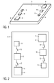
- the chip terminals 6, 7 are arranged on the substrate surface 5 of the chip substrate 4 and have each a rectangular area A for the exemplary embodiment, as is shown in Figures 1 and 2 , wherein Fig. 2 is a top view of the semiconductor chip 1 at the fabrication step of Fig. 1 .
- the semiconductor chip 1 comprises a first conductive area 8, a second conductive area 9, a third conductive area 10 and a fourth conductive area 11, which all are deposited on the substrate surface 5 by well known deposition techniques.
- the first and third conductive areas 8, 10 have each a rectangular shape and are smaller than the areas A of the first and second chip terminals 6, 7.
- the second and fourth conductive areas 9, 11 have each a rectangular shape and are smaller than the first and third conductive areas 8, 10, as is evident from Fig. 2 .
- the first chip terminal 6 and the first conductive area 8 can be electrically connected by a first switch 12, the first conductive area 8 and the second conductive area 9 can be electrically connected by a second switch 13, the second chip terminal 7 and the third conductive area 10 can be electrically connected by a third switch 14, and the third conductive area 10 and the fourth conductive area 11 can be electrically connected by a fourth switch 15.
- the switches 12 to 15 are integrated within the chip substrate 4 and are based on transistor technology for the exemplary embodiment.
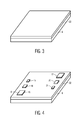
- a passivation layer 22 is deposited on the substrate surface 5 completely covering the chip terminals 6, 7 and the conductive areas 8-11, as is shown in Fig. 3 .
- the passivation layer 22 is a sealing layer to prevent deterioration of electric properties of the semiconductor chip 1 through chemical action, corrosion, or handling during a packing process.
- the passivation layer 22 also protects the semiconductor chip 1 against moisture or contamination.
- the passivation layer 22 is a layer of silicon nitride and is about 900 nm thick. Another suitable material for the passivation layer 22 is, for instance, silicon dioxide.
- a first bump 16 is deposited on the passivation layer 22 directly above the first chip terminal 6, as is shown in Fig. 4 and in Fig. 5 , which is a cross-sectional view of the semiconductor chip 1.
- the distance d is 900 nm and the areas A and A' of the first chip terminal 6 and the first bump 16, respectively, are 3600 pm 2 (square-picometer) for the exemplary embodiment.
- the capacitance C 1 is approximately 142 fF (Femto-Farad).
- a second bump 17 made of gold is deposited on the passivation layer 22 directly above the second chip terminal 7.
- the second bump 17 is also square-shaped and has an area A' substantially equal to the areas A of the first and second chip terminals 6, 7.
- the second bump 17 is spaced apart from the second chip terminal 7 by the same distance d and forms, with the second chip terminal 7 and the intermediate passivation layer 22, a second capacitor with the capacitance C 2 , which also equals approximately 142 fF (Femto-Farad).
- the first conductive area 8, the third bump 18 and the intermediate passivation layer 22 form a third capacitor, whose capacitance C 3 is smaller than the capacitance C 1 or C 2 .
- the second conductive area 9, the fourth bump 19 and the intermediate passivation layer 22 form a fourth capacitor, whose capacitance C 4 is smaller than the capacitance C 3 .
- the third conductive area 10, the fifth bump 20 and the intermediate passivation layer 22 form a fifth capacitor, whose capacitance C 5 approximately equals the capacitance C 3 and the fourth conductive area 11, the sixth bump 21 and the intermediate passivation layer 22 form a sixth capacitor whose capacitance C 6 approximately equals the capacitance C 4 .
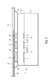
- the semiconductor chip 1 is meant to be combined with the antenna 2 to the transponder 3, which is depicted in Figures 6 and 7 in a cross-sectional view.
- Fig. 8 shows the antenna 2 in a top view.
- the antenna 2 is a dipole antenna, comprised of a first conductive trace 26 and a second conductive trace 27 made of metal.
- One end of the first conductive trace 26 is a first antenna terminal 24 and one end of the second conductive trace 27 is a second antenna terminal 25.
- the conductive traces 26, 27 are attached to an antenna substrate 23 for the exemplary embodiment, as is commonly known in the art.
- the antenna substrate 23 is, for instance, a plastic sheet.
- the conductive trances 26, 27 are connected by a conductive loop 28 made of metal and attached to the substrate 23 for the exemplary embodiment.
- the conductive loop has an inductance L.
- the antenna 2 is attached to the passivation layer 22 such that the first antenna terminal 24 touches the first, third and fourth bumps 16, 18, 19, and the second antenna terminal 25 touches the second, fifth, and sixth bumps 17, 20, 21.
- the antenna substrate 23 with the conductive traces 26, 27 and the conductive loop 28 are fixed to the semiconductor chip 1 by means of a glue which forms a glue layer 29.
- the glue comprises conductive particles (e.g. conductive balls in a non conductive gluey material), so that an electrical contact is established between the bumps 16-21 when the antenna substrate 23 is pressed against the passivation layer 22 and the bumps 16-21.
- the first, third, and fourth bumps 16, 18, 19 are connected in series by the first conductive trace 26, as is shown in Fig. 8
- the second, fifth, and sixth bumps 17, 20, 21 are also connected in series by the second conductive trace 27 for the exemplary embodiment.
- the conductive particles do not form a conductive chain.
- the great advantage is that filling the gaps between the bumps 16-21 and attaching the antenna substrate 23 to the chip 1 may be performed in one single process step.
- a non-conductive underfill material may be applied to the gaps between the bumps 16-21 after the fabrication of the bumps 16-21, so that an even surface is obtained.
- the antenna substrate 23 is joined to the chip 1 by means of a conductive glue, which then forms a comparable thin layer between said surface and the antenna substrate 23 and said surface and the antenna terminals 24, 25 (not shown in Figs.) respectively.
- the resulting capacitance, C 2,res at the second antenna terminal 25 can be adjusted by appropriately closing the third and fourth switches 14, 15.
- Fig. 9 shows a second exemplary embodiment of a semiconductor chip 91, which can be combined with the antenna 2 to a second exemplary embodiment of a transponder 93 whose cross-sectional view is shown in Figures 10 and 11 . If not especially stated, then components of the semiconductor chip 91 and components of the transponder 93 are denoted by the same reference signs as components of the semiconductor chip 1 and the transponder 3.
- the semiconductor chip 91 of Fig. 9 does not comprise the switches 12-15. Instead, the chip terminals 6, 7 and the conductive areas 8-11 are permanently interconnected by connectors.
- Fig. 9 shows only a connector 94 electrically connecting the first chip terminal 6 to the first conductive area 8 and a connector 95 electrically connecting the first conductive area 8 to the second conductive area 9.
- the antenna 2 of the exemplary embodiments described is a dipole antenna.
- the invention is, however, not restricted to such antenna structures and other antenna structures are within the scope of the invention.
- the described capacitors C 1 to C 5 are connected in series for the exemplary embodiments described.
- the bumps or the antenna structure can also be designed in such a way that these capacitors are connected in parallel or as a combination of the two.
- the embodiment shown just allows to change the capacitance by discrete steps
- the capacitance can be changed continuously by partly taking away said second plate or by just dividing said second plate into two parts at an arbitrary location, e.g. by means of a laser.
- the change of the capacitance is not limited to discrete steps, that is to say just limited to the resolution of the removing or dividing process.
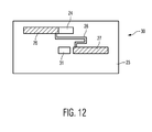
- Fig. 12 shows a further exemplary embodiment of an antenna 30. If not especially stated, then components of the antenna 30 are denoted by the same reference signs as components of the antenna 2.
- the antenna 30 is also a dipole antenna. Compared to the antenna 2, the bumps 20, 21 are not connected by the second conductive trace 27, but by a third conductive trace 31.
- the corresponding capacitors C 5 and C 6 are connected to the circuitry of the semiconductor chips 1, 91, in order to trim this circuitry.
Landscapes
- Engineering & Computer Science (AREA)
- Microelectronics & Electronic Packaging (AREA)
- Computer Hardware Design (AREA)
- Physics & Mathematics (AREA)
- General Physics & Mathematics (AREA)
- Theoretical Computer Science (AREA)
- Semiconductor Integrated Circuits (AREA)
Description
- The invention relates to a semiconductor chip, a transponder, and to a method of manufacturing a transponder.
- Published German patent application
101 33 588 A1 discloses a semiconductor chip arranged on a chip carrier and an antenna. The chip carrier and the antenna have each conductive surfaces, which are glued together by means of a non-conductive glue layer, so that the conductive surfaces are coupled capacitively. The conductive surfaces and the intermediate non-conductive glue layer constitute capacitors whose capacitances are determined, inter alia, by the thickness of the glue layer. The glue layer, however, cannot be applied accurately within a certain thickness, resulting in varying capacitances of different chips including the antenna. - International Patent Application Publication no
WO02/50890 - International Patent Application Publication no
WO2006/09934 - It is an object of the invention to provide a semiconductor chip for a transponder whose antenna is coupled capacitively to the chip, wherein said chip is designed such that this capacitive coupling can, in a relatively simple manner, be established with a predefined capacitance having a relatively small tolerance.
- A further object of the invention is to provide a corresponding method of manufacturing such a transponder.
- The object of the invention is achieved by means of a semiconductor chip for a transponder, as defined in
claim 1. - The inventive chip is supposed to be used in combination with an antenna to form a transponder. The antenna may capture a signal to be processed by circuitry of the chip or this circuitry may generate a signal to be emitted by the antenna. For this purpose, the antenna and the chip terminals are coupled capacitively. This coupling may be modelled by the first capacitors between the chip terminals and the antenna terminals. The corresponding capacitance depends, inter alia, on the thickness of a dielectric between the antenna terminals and the chip terminals. According to the invention, this dielectric is formed by the passivation layer covering the surface of the inventive chip and the chip terminals.
- Generally, a passivation layer is a sealing layer to prevent deterioration of electric properties of the inventive semiconductor chip through chemical action, corrosion, or handling during a packing process. The passivation layer also protects the semiconductor chip against moisture or contamination. Suitable materials for a passivation layer include silicon nitride and silicon dioxide. The advantage of such a passivation layer is that it can be deposited on the substrate surface within a relatively small tolerance by well known methods. Consequently, the passivation layer can be applied on the substrate surface with a predefined thickness having a relatively small tolerance, resulting in a capacitive coupling of the chip terminal and the antenna with a predefined capacitance having a relatively small tolerance.
- The passivation layer may particularly be a single homogeneous layer which partially or completely covers the substrate surface and completely covers the chip terminals. The passivation layer may also be one layer being comprised of different partial layers adjoining each other so that, for instance, one of the partial layers completely covers each chip terminal and another partial layer partially or completely covers the remaining substrate surface. Then, the material for the partial layer completely covering the chip terminals can be chosen to be especially suitable as a dielectric.
- The inventive chip is meant to be combined with the antenna to form a transponder. Since the antenna and the chip terminals are coupled capacitively, the chip terminals do not need to be exposed for a galvanic coupling of the chip terminals and the antenna by, for instance, etching the passivation layer. Hence, one step in the fabrication process of the chip may be saved.
- The antenna may be a loop antenna. Then conventional chips comprise necessary internal capacitors inside the semiconductor chip, which internal capacitors are connected in series to the antenna for preventing a d.c. short circuit. Since the inventive semiconductor chip is designed for a capacitive coupling between the chip and the antenna, such internal capacitors can be omitted. This may result in a reduced layout of the chip and thus a reduced chip area needed for the electronic parts.
- The inventive semiconductor chip may comprise first bumps to be electrically connected to the antenna terminals. The first bumps are deposited on the passivation layer above the chip terminals. The first bumps are electrically conductive and may be made of gold. Due to the first bumps, the distance between the antenna and the chip terminals is smaller than the distance between the antenna and the remaining substrate surface. This may result in reduced stray capacitances between the chip terminals and the antenna and may reduce the tolerance of the desired capacitance between the chip terminals and the antenna. The space between the passivation layer and the antenna at areas where no bumps are deposited on the passivation layer my be filled with an appropriate underfill material.
- The inventive semiconductor chip may comprise, on the surface and covered completely by the passivation layer, conductive areas, which form second capacitors with the antenna when the antenna is attached to the chip and/or which conductive areas form third capacitors with a conductive structure. The antenna and conductive areas may be formed such that the second capacitors can be connected in series and/or in parallel to the first capacitors formed by the chip terminals, the antenna terminals and the intermediate passivation layer by, for instance, electrically connecting conductive areas to the chip terminals or by interconnecting at least some of the conductive areas. The second capacitors, which may form binary stepped capacitors, can be used to tune the antenna to a desired resonance frequency. Thus, tolerances of the chip, the antenna, or the resulting capacitance during assembling of the resulting transponder may be compensated.
- If the conductive areas are connected together with a conductive structure, which may be deposited on a substrate of the antenna, then these resulting third capacitors can be used, for instance, as capacitors trimming circuitry of the semiconductor chip inside the chip substrate. Thus, these capacitors may be used for an application, which is different from the antenna coupling. Advantageously, chip area may be saved because just one plate of each capacitor is indeed within the chip. The other plate is outside the chip, arranged on the, for instance, antenna substrate.
- In a restricted version, the inventive semiconductor chip comprises switches for electrically connecting at least one of the conductive areas to the chip terminals or for electrically interconnecting at least some of the conductive areas. Then, the assembled transponder comprising the antenna and the inventive semiconductor chip can relatively easily be tuned by opening and closing these switches. The switches may be diode switches or transistor switches particularly integrated into the substrate.
- The inventive semiconductor chip may comprise second bumps to be electrically connected to the antenna and/or the conductive structure. The second bumps are deposited on the passivation layer above the conductive areas. Then, the resulting second and/or third capacitors may be fabricated with a relatively small tolerance.
- The object of the invention is also achieved by means of a transponder, comprising the inventive semiconductor chip and an antenna with antenna terminals attached to the chip above the chip terminals, so that the chip terminals, the passivation layer and the antenna terminals form the first capacitors. The antenna terminals may be electrically connected to the first bumps and/or the antenna may be electrically connected to the second bumps. Then, the resulting capacitance at the respective chip terminals are determined by the combination of the first and second capacitors, which may particularly be connected in series and/or in parallel to the first capacitors.
- The antenna may be attached to the passivation layer by means of a conductive or a non-conductive glue. The conductive glue assures a good electrical contact between the antenna and the bumps.
- The antenna may be inductive, has an inductance, or may comprise an additional inductance, so that a resulting resonance frequency of the inductance in combination with the first and second capacitors results in a resonance frequency. This resonance frequency may be tunable by establishing electrical connections between the chip terminals and the conductive areas and/or by breaking the antenna structure of the antenna, which antenna structure connects the second bumps.
- The object of the invention is also achieved by means of a method of manufacturing a transponder, the method comprising the steps of:
- depositing a passivation layer on a surface of a chip substrate; the surface comprising chip terminals and the passivation layer covering the surface and completely covering the chip terminals; and
- attaching, to the passivation layer at least indirectly, antenna terminals of an antenna above the chip terminals, so that the chip terminals, the antenna terminals, and the passivation layer form first capacitors.
- The inventive method may comprise, before attaching the antenna terminals to the passivation layer, the following steps:
- depositing conductive areas on the surface;
- depositing the passivation layer on the surface of the chip substrate, so that the passivation layer covers the surface, the chip terminals, and the conductive areas;
- depositing first bumps on the passivation layer, above the chip terminals,
- depositing second bumps on the passivation layer, above the conductive areas; and
- electrically connecting the first bumps to the antenna terminals and the second bumps to the antenna.
- The invention will be described in greater detail hereinafter, by way of nonlimiting examples, with reference to the embodiments shown in the drawings.
-
Figs. 1 to 5 are different steps illustrating the fabrication of a first exemplary embodiment of an inventive semiconductor chip; -
Figs. 6 ,7 are cross-sectional views of a first exemplary embodiment of an inventive transponder comprising the semiconductor chip ofFigs. 1 to 5 and an antenna; -
Fig. 8 is a top view of the antenna of the transponder ofFigs. 6 and7 ; -
Fig. 9 is a cross-sectional view of a second exemplary embodiment of an inventive semiconductor chip; -
Figs. 10 ,11 are cross-sectional views of a second exemplary embodiment of an inventive transponder comprising the semiconductor chip ofFig. 9 ; and -
Fig. 12 is a top view of a further antenna. -
Figures 1 to 5 show steps for manufacturing asemiconductor chip 1, which is to be combined with anantenna 2 to atransponder 3 shown inFigures 6 and7 . Thefinished semiconductor chip 1 is depicted inFigures 4 and5 and a top view of theantenna 2 is shown inFig. 8 . - The
semiconductor chip 1 comprises achip substrate 4 with asubstrate surface 5. Thechip substrate 4 includes, as is commonly known, circuitry not shown in the Figures. When thetransponder 3 is finished, then the circuitry of thesemiconductor chip 1 is coupled capacitively to theantenna 2 via afirst chip terminal 6 and asecond chip terminal 7. Thechip terminals substrate surface 5 of thechip substrate 4 and have each a rectangular area A for the exemplary embodiment, as is shown inFigures 1 and 2 , whereinFig. 2 is a top view of thesemiconductor chip 1 at the fabrication step ofFig. 1 . - For the exemplary embodiment, the
semiconductor chip 1 comprises a firstconductive area 8, a secondconductive area 9, a thirdconductive area 10 and a fourthconductive area 11, which all are deposited on thesubstrate surface 5 by well known deposition techniques. The first and thirdconductive areas second chip terminals conductive areas conductive areas Fig. 2 . - For the exemplary embodiment, the
first chip terminal 6 and the firstconductive area 8 can be electrically connected by afirst switch 12, the firstconductive area 8 and the secondconductive area 9 can be electrically connected by asecond switch 13, thesecond chip terminal 7 and the thirdconductive area 10 can be electrically connected by athird switch 14, and the thirdconductive area 10 and the fourthconductive area 11 can be electrically connected by afourth switch 15. Theswitches 12 to 15 are integrated within thechip substrate 4 and are based on transistor technology for the exemplary embodiment. - In a further fabrication step, a
passivation layer 22 is deposited on thesubstrate surface 5 completely covering thechip terminals Fig. 3 . Thepassivation layer 22 is a sealing layer to prevent deterioration of electric properties of thesemiconductor chip 1 through chemical action, corrosion, or handling during a packing process. Thepassivation layer 22 also protects thesemiconductor chip 1 against moisture or contamination. For the exemplary embodiment, thepassivation layer 22 is a layer of silicon nitride and is about 900 nm thick. Another suitable material for thepassivation layer 22 is, for instance, silicon dioxide. - After that, a
first bump 16 is deposited on thepassivation layer 22 directly above thefirst chip terminal 6, as is shown inFig. 4 and inFig. 5 , which is a cross-sectional view of thesemiconductor chip 1. For the exemplary embodiment, thefirst bump 16 is made of gold, has an rectangular area A' substantially equal to the area A of thefirst chip terminal 6 and forms, together with thefirst chip terminal 6 and theintermediate passivation layer 22, a first capacitor having the capacitance, C1, of:
wherein ε0 is the permittivity of free space which equals
approximately 8.8541878176 * 10-12 F/m, εr is the relative permittivity of the material of thepassivation layer 22 and equals approximately 4 for the exemplary embodiment, and d is the distance between thefirst chip terminal 6 and thefirst bump 16. The distance d is 900 nm and the areas A and A' of thefirst chip terminal 6 and thefirst bump 16, respectively, are 3600 pm2 (square-picometer) for the exemplary embodiment. Thus, the capacitance C1 is approximately 142 fF (Femto-Farad). - For the exemplary embodiment, a
second bump 17 made of gold is deposited on thepassivation layer 22 directly above thesecond chip terminal 7. Thesecond bump 17 is also square-shaped and has an area A' substantially equal to the areas A of the first andsecond chip terminals second bump 17 is spaced apart from thesecond chip terminal 7 by the same distance d and forms, with thesecond chip terminal 7 and theintermediate passivation layer 22, a second capacitor with the capacitance C2, which also equals approximately 142 fF (Femto-Farad). - For the exemplary embodiment, the
semiconductor chip 1 comprises athird bump 18, which is made of gold and is deposited on thepassivation layer 22 directly above the firstconductive area 8, afourth bump 19, which is made of gold and is deposited on thepassivation layer 22 directly above the secondconductive area 9, afifth bump 20, which is made of gold and is deposited on thepassivation layer 22 directly above the thirdconductive area 10, and asixth bump 21, which is made of gold and is deposited on thepassivation layer 22 directly above the fourthconductive area 11. The respective third to sixth bumps 18-21 have areas corresponding to the respective first to fourth conductive areas 8-11. The firstconductive area 8, thethird bump 18 and theintermediate passivation layer 22 form a third capacitor, whose capacitance C3 is smaller than the capacitance C1 or C2. The secondconductive area 9, thefourth bump 19 and theintermediate passivation layer 22 form a fourth capacitor, whose capacitance C4 is smaller than the capacitance C3. The thirdconductive area 10, thefifth bump 20 and theintermediate passivation layer 22 form a fifth capacitor, whose capacitance C5 approximately equals the capacitance C3 and the fourthconductive area 11, thesixth bump 21 and theintermediate passivation layer 22 form a sixth capacitor whose capacitance C6 approximately equals the capacitance C4. - The
semiconductor chip 1 is meant to be combined with theantenna 2 to thetransponder 3, which is depicted inFigures 6 and7 in a cross-sectional view. -
Fig. 8 shows theantenna 2 in a top view. For the exemplary embodiment, theantenna 2 is a dipole antenna, comprised of a firstconductive trace 26 and a secondconductive trace 27 made of metal. One end of the firstconductive trace 26 is afirst antenna terminal 24 and one end of the secondconductive trace 27 is asecond antenna terminal 25. The conductive traces 26, 27 are attached to anantenna substrate 23 for the exemplary embodiment, as is commonly known in the art. Theantenna substrate 23 is, for instance, a plastic sheet. Additionally, theconductive trances conductive loop 28 made of metal and attached to thesubstrate 23 for the exemplary embodiment. The conductive loop has an inductance L. - In order to obtain the
transponder 3, theantenna 2 is attached to thepassivation layer 22 such that thefirst antenna terminal 24 touches the first, third andfourth bumps second antenna terminal 25 touches the second, fifth, andsixth bumps antenna substrate 23 with the conductive traces 26, 27 and theconductive loop 28 are fixed to thesemiconductor chip 1 by means of a glue which forms aglue layer 29. For the exemplary embodiment, the glue comprises conductive particles (e.g. conductive balls in a non conductive gluey material), so that an electrical contact is established between the bumps 16-21 when theantenna substrate 23 is pressed against thepassivation layer 22 and the bumps 16-21. As a result, the first, third, andfourth bumps conductive trace 26, as is shown inFig. 8 , and the second, fifth, andsixth bumps conductive trace 27 for the exemplary embodiment. In areas where the glue is less compressed (i.e. in the gaps between the bumps 16-21), the conductive particles do not form a conductive chain. The great advantage is that filling the gaps between the bumps 16-21 and attaching theantenna substrate 23 to thechip 1 may be performed in one single process step. However, it is also imaginable to use a non-conductive glue for theglue layer 29. In this case theantenna terminals antenna substrate 23 is joined to thechip 1 by means of a conductive glue, which then forms a comparable thin layer between said surface and theantenna substrate 23 and said surface and theantenna terminals 24, 25 (not shown in Figs.) respectively. - As mentioned above, the
semiconductor chip 1 comprises switches 12-15 for electrically connecting thechip terminals conductive areas conductive areas conductive areas second switches first antenna terminal 24 can be adjusted. For example, if thefirst switch 12 is closed and thesecond switch 13 is open, as is illustrated inFig. 2 ,Fig. 5 , andFig. 7 , then the resulting capacitance, C1,res at thefirst antenna terminal 24 equals:
- The resulting capacitance, C2,res at the
second antenna terminal 25 can be adjusted by appropriately closing the third andfourth switches Fig. 2 , the third andfourth switches second antenna terminal 25 can be calculated according to:
-
Fig. 9 shows a second exemplary embodiment of asemiconductor chip 91, which can be combined with theantenna 2 to a second exemplary embodiment of atransponder 93 whose cross-sectional view is shown inFigures 10 and11 . If not especially stated, then components of thesemiconductor chip 91 and components of thetransponder 93 are denoted by the same reference signs as components of thesemiconductor chip 1 and thetransponder 3. - Compared to the
semiconductor chip 1 ofFig. 4 , thesemiconductor chip 91 ofFig. 9 does not comprise the switches 12-15. Instead, thechip terminals Fig. 9 shows only aconnector 94 electrically connecting thefirst chip terminal 6 to the firstconductive area 8 and aconnector 95 electrically connecting the firstconductive area 8 to the secondconductive area 9. Thus, the resulting capacitances, C1,res, C2,res at theantenna terminals transponder 93 can be calculated according to:

- In order to adjust the resulting capacitances, C1,res, C2,res at the
antenna terminals transponder 93, the conductive traces 26, 27 of theantenna 2 can be broken at predefined locations to break a connection between two bumps.Fig. 11 shows an example where theconductive trace 26 is broken at alocation 92 between the third andfourth bumps first antenna terminal 24 equals:
- The
antenna 2 of the exemplary embodiments described is a dipole antenna. The invention is, however, not restricted to such antenna structures and other antenna structures are within the scope of the invention. The described capacitors C1 to C5 are connected in series for the exemplary embodiments described. The bumps or the antenna structure can also be designed in such a way that these capacitors are connected in parallel or as a combination of the two. - Although, the embodiment shown just allows to change the capacitance by discrete steps, one skilled in the art can easily imagine that by forming one plate of a capacitor on the
chip substrate 4 and the second plate on theantenna substrate 23, the capacitance can be changed continuously by partly taking away said second plate or by just dividing said second plate into two parts at an arbitrary location, e.g. by means of a laser. By doing so, the change of the capacitance is not limited to discrete steps, that is to say just limited to the resolution of the removing or dividing process. -
Fig. 12 shows a further exemplary embodiment of anantenna 30. If not especially stated, then components of theantenna 30 are denoted by the same reference signs as components of theantenna 2. Theantenna 30 is also a dipole antenna. Compared to theantenna 2, thebumps conductive trace 27, but by a thirdconductive trace 31. The corresponding capacitors C5 and C6 are connected to the circuitry of thesemiconductor chips - Finally, it should be noted that the above-mentioned embodiments illustrate rather than limit the invention, and that those skilled in the art will be capable of designing many alternative embodiments without departing from the scope of the invention as defined by the appended claims. In the claims, any reference signs placed in parentheses shall not be construed as limiting the claims. The words "comprising" and "comprises", and the like, do not exclude the presence of elements or steps other than those listed in any claim or the specification as a whole. The singular reference of an element does not exclude the plural reference of such elements and vice-versa. In a device claim enumerating several means, several of these means may be embodied by one and the same item of hardware. The mere fact that certain measures are recited in mutually different dependent claims does not indicate that a combination of these measures cannot be used to advantage.
Claims (14)
- A semiconductor chip for a transponder (3, 93), the chip comprising:a chip substrate (4) with a surface (5);chip terminals (6, 7) arranged on said surface (5);characterised in that the chip further comprisesa passivation layer (22) covering said surface (5) and completely covering said chip terminals (6, 7), so that an antenna (2, 30) with antenna terminals (24, 25) can be attached to said chip (1, 91) above said chip terminals (6, 7), so that said chip terminals (6, 7), said passivation layer (22) and said antenna terminals (24, 25) form first capacitors.
- The chip of claim 1, comprising first bumps (16, 17) to be electrically connected to said antenna terminals (24, 25); said first bumps (16, 17) being deposited on said passivation layer (22) above said chip terminals (6, 7).
- The chip of claim 1, comprising, on said surface (5) and completely covered by said passivation layer (22), conductive areas (8-11) which form second capacitors with said antenna (2, 30) when said antenna (2, 30) is attached to said chip (1, 91) and/or which conductive areas (8-11) form third capacitors with a conductive structure (31).
- The chip of claim 3, wherein at least one of said conductive areas (8-11) is electrically connected to said chip terminals (6, 7) or at least some of said conductive areas (8-11) are electrically interconnected.
- The chip of claim 3, comprising switches (12-15) for electrically connecting at least one of said conductive areas (8-11) to said chip terminals (6, 7) or for electrically interconnecting at least some of said conductive areas (8-11).
- The chip of claim 3, wherein said conductive areas (8-11) are such that their corresponding second capacitors form binary stepped capacitors.
- The chip of claim 3, comprising second bumps (18-21) to be electrically connected to said antenna (2, 30) and/or said conductive structure (31); said second bumps (18-21) being deposited on said passivation layer (22) above said conductive areas (18-21).
- A transponder, comprising:said chip (1, 91) of any one of claims 1 to 7; andan antenna (2, 30) with antenna terminals (24, 25) attached to said chip (1, 91) above said chip terminals (6, 7)so that said chip terminals (6, 7), said passivation layer (22) and said antenna terminals (24, 25) form said first capacitors.
- The transponder of claim 8, when dependent on claim 2 or claim 7, wherein said antenna terminals (24, 25) and/or said antenna (2, 30) are electrically connected to said first bumps (16, 17) or to said second bumps (18-21) respectively.
- The transponder of claim 8, wherein said antenna (2, 30) is attached to said passivation layer (22) by means of a conductive or a non-conductive glue (29).
- The transponder of claim 8, when dependent on one of claims 3 to 7, further comprising first bumps (16,17) to be connected electrically to said antenna terminals (24,25); said first bumps (16,17) being deposited on said passivation layer (22) above said chip terminals (6,7), wherein said antenna (2, 30) is inductive, has an inductance, or comprises an additional inductance (28), so that a combination of (a) said inductance or said additional inductance and (b)said first and second capacitors results in a resonance frequency which is tunable by establishing electrical connections between said chip terminals (6, 7) and said conductive areas (8-11) and/or by breaking the antenna structure (92) of said antenna (2, 30), which antenna structure either connects said second bumps (18-21) or connects said first bumps (16, 17) to said second bumps (18-21).
- A method of manufacturing a transponder, the method comprising the steps of:depositing a passivation layer (22) on a surface (5) of a chip substrate (4); said surface (5) comprising chip terminals (6, 7) and said passivation layer (22) completely covering said surface (5) and covering said chip terminals (6, 7); andattaching, to said passivation layer (22) at least indirectly, antenna terminals (24, 25) of an antenna (2, 30) above said chip terminals (6, 7), so that said chip terminals (6, 7), said antenna terminals (24, 25), and said passivation layer (22) constitute first capacitors.
- The method of claim 12, comprising, before attaching said antenna terminals (24, 25) to said passivation layer (22), the steps of:depositing, on said passivation layer (22), bumps (16, 17) above said chip terminals (6, 7); andelectrically connecting said bumps (16, 17) to said antenna terminals (24, 25).
- The method of claim 12, comprising, before attaching said antenna terminals (24, 25) to said passivation layer (22), the following steps of:depositing conductive areas (8-11) on said surface (5);depositing said passivation layer (22) on said surface (5) of said chip substrate (4), so that said passivation layer (22) covers said surface (5), said chip terminals (6, 7), and said conductive areas (8-11);depositing first bumps (16, 17) on said passivation layer (22), above said chip terminals (6, 7),depositing second bumps (18-21) on said passivation layer (22), above said conductive areas (8-11); andelectrically connecting said first bumps (16, 17) to said antenna terminals (24, 25) and said second bumps (18-21) to said antenna (22).
Priority Applications (1)
| Application Number | Priority Date | Filing Date | Title |
|---|---|---|---|
| EP07735948.7A EP2038817B1 (en) | 2006-06-07 | 2007-05-16 | Semiconductor chip, transponder and method of manufacturing a transponder |
Applications Claiming Priority (3)
| Application Number | Priority Date | Filing Date | Title |
|---|---|---|---|
| EP06115080 | 2006-06-07 | ||
| EP07735948.7A EP2038817B1 (en) | 2006-06-07 | 2007-05-16 | Semiconductor chip, transponder and method of manufacturing a transponder |
| PCT/IB2007/051884 WO2007141686A1 (en) | 2006-06-07 | 2007-05-16 | Semiconductor chip, transponder and method of manufacturing a transponder |
Publications (2)
| Publication Number | Publication Date |
|---|---|
| EP2038817A1 EP2038817A1 (en) | 2009-03-25 |
| EP2038817B1 true EP2038817B1 (en) | 2015-04-01 |
Family
ID=38556390
Family Applications (1)
| Application Number | Title | Priority Date | Filing Date |
|---|---|---|---|
| EP07735948.7A Active EP2038817B1 (en) | 2006-06-07 | 2007-05-16 | Semiconductor chip, transponder and method of manufacturing a transponder |
Country Status (5)
| Country | Link |
|---|---|
| US (1) | US9047548B2 (en) |
| EP (1) | EP2038817B1 (en) |
| JP (1) | JP2009540418A (en) |
| CN (1) | CN101467162B (en) |
| WO (1) | WO2007141686A1 (en) |
Families Citing this family (7)
| Publication number | Priority date | Publication date | Assignee | Title |
|---|---|---|---|---|
| FR2927441B1 (en) * | 2008-02-13 | 2011-06-17 | Yannick Grasset | CONTACTLESS OBJECT WITH INTEGRATED CIRCUIT CONNECTED TO THE TERMINALS OF A CIRCUIT BY CAPACITIVE COUPLING |
| KR102287869B1 (en) * | 2013-11-18 | 2021-08-09 | 컴포시큐어 엘엘씨 | Card with a metal layer and an antenna |
| EP3146476B1 (en) | 2014-05-22 | 2026-02-18 | Composecure LLC | Transaction and id cards having selected texture and coloring |
| US10783422B2 (en) | 2014-11-03 | 2020-09-22 | Composecure, Llc | Ceramic-containing and ceramic composite transaction cards |
| CN107111413B (en) * | 2015-01-29 | 2020-02-07 | 株式会社和冠 | Electrostatic pen |
| CN110970711A (en) * | 2018-09-28 | 2020-04-07 | 日本电产株式会社 | Antenna element and antenna array |
| US20200212536A1 (en) * | 2018-12-31 | 2020-07-02 | Texas Instruments Incorporated | Wireless communication device with antenna on package |
Family Cites Families (17)
| Publication number | Priority date | Publication date | Assignee | Title |
|---|---|---|---|---|
| US5430441A (en) * | 1993-10-12 | 1995-07-04 | Motorola, Inc. | Transponding tag and method |
| JPH07321550A (en) | 1994-05-20 | 1995-12-08 | Murata Mfg Co Ltd | Antenna system |
| JP3150575B2 (en) | 1995-07-18 | 2001-03-26 | 沖電気工業株式会社 | Tag device and manufacturing method thereof |
| KR20000049028A (en) | 1996-10-09 | 2000-07-25 | 피에이브이 카드 게엠베하 | Method and connection arrangement for producing a smart card |
| WO1998040930A1 (en) | 1997-03-10 | 1998-09-17 | Precision Dynamics Corporation | Reactively coupled elements in circuits on flexible substrates |
| JP2003523700A (en) * | 2000-02-14 | 2003-08-05 | コーニンクレッカ フィリップス エレクトロニクス エヌ ヴィ | Transponders and appliances |
| DE10064411A1 (en) | 2000-12-21 | 2002-06-27 | Giesecke & Devrient Gmbh | Electrically conductive connection between a chip and a coupling element as well as security element, security paper and document of value with such a connection |
| US6407669B1 (en) | 2001-02-02 | 2002-06-18 | 3M Innovative Properties Company | RFID tag device and method of manufacturing |
| DE10108080C1 (en) * | 2001-02-20 | 2002-04-04 | Infineon Technologies Ag | Contactless data carrier with capacitively coupled antenna coil has spacer elements between IC substrate contacts and cooperating coil terminals |
| US6815809B2 (en) | 2001-03-16 | 2004-11-09 | Koninklijke Philips Electronics N.V. | Portable electronic device |
| ATE448527T1 (en) | 2001-04-26 | 2009-11-15 | Nxp Bv | DATA CARRIER WITH AN INTEGRATED CIRCUIT WITH INTEGRATED MAIN CAPACITY AND WITH ADDITIONAL INTEGRATED CAPACITIES |
| DE10133588A1 (en) | 2001-07-11 | 2002-09-05 | Infineon Technologies Ag | Semiconductor chip and conductive structure for contactless chip cards has capacitive coupling between integrated circuit and coil antenna |
| US6900536B1 (en) | 2002-04-26 | 2005-05-31 | Celis Semiconductor Corporation | Method for producing an electrical circuit |
| US7224280B2 (en) | 2002-12-31 | 2007-05-29 | Avery Dennison Corporation | RFID device and method of forming |
| JP2005093867A (en) * | 2003-09-19 | 2005-04-07 | Seiko Epson Corp | Semiconductor device and manufacturing method thereof |
| DE102004034768B4 (en) | 2004-07-19 | 2007-11-15 | Infineon Technologies Ag | Identification media |
| DE102005017655B4 (en) * | 2005-04-15 | 2008-12-11 | Polyic Gmbh & Co. Kg | Multilayer composite body with electronic function |
-
2007
- 2007-05-16 CN CN2007800213311A patent/CN101467162B/en not_active Expired - Fee Related
- 2007-05-16 WO PCT/IB2007/051884 patent/WO2007141686A1/en not_active Ceased
- 2007-05-16 US US12/303,705 patent/US9047548B2/en active Active
- 2007-05-16 JP JP2009513810A patent/JP2009540418A/en not_active Withdrawn
- 2007-05-16 EP EP07735948.7A patent/EP2038817B1/en active Active
Also Published As
| Publication number | Publication date |
|---|---|
| JP2009540418A (en) | 2009-11-19 |
| US20100224959A1 (en) | 2010-09-09 |
| CN101467162A (en) | 2009-06-24 |
| EP2038817A1 (en) | 2009-03-25 |
| CN101467162B (en) | 2011-11-23 |
| WO2007141686A1 (en) | 2007-12-13 |
| US9047548B2 (en) | 2015-06-02 |
Similar Documents
| Publication | Publication Date | Title |
|---|---|---|
| US7871008B2 (en) | Wireless IC device and manufacturing method thereof | |
| US9047548B2 (en) | Semiconductor chip, transponder and method of manufacturing a transponder | |
| DE102005053765B4 (en) | MEMS package and method of manufacture | |
| US7931206B2 (en) | Wireless IC device | |
| US7750862B2 (en) | Broadband antenna for a transponder of a radio frequency identification system | |
| US7988059B2 (en) | Method for connecting an electronic chip to a radiofrequency identification device | |
| GB2303523A (en) | Solderless tag device with integral capacitance between IC and antenna terminals | |
| US20220368003A1 (en) | Antenna module and manufacturing method thereof | |
| US12205858B2 (en) | Electronic component module and method for manufacturing electronic component module | |
| US12201028B2 (en) | Mountable electronic component and electronic circuit module | |
| US20110073357A1 (en) | Electronic device and method of manufacturing an electronic device | |
| US9779349B2 (en) | Method of producing a transponder and a transponder | |
| US9142485B2 (en) | Contactless object with integrated circuit connected to circuit terminals by capacitive coupling | |
| DE102008049371A1 (en) | Device with an RFID transponder in an electrically conductive object and manufacturing method thereof | |
| US9608307B2 (en) | Semiconductor substrate-based system for an RFID device, RFID device, and method for manufacturing such a semiconductor substrate-based system | |
| US8136737B2 (en) | System comprised of a chip and a substrate and method of assembling such a system | |
| CN114285391B (en) | Radio frequency filter and manufacturing method thereof | |
| US20080122074A1 (en) | Multi-chip electronic circuit module and a method of manufacturing | |
| DE102005063640B3 (en) | MEMS package and method of manufacture | |
| US20080061404A1 (en) | Electronic circuit package and fabricating method thereof | |
| US20110163442A1 (en) | Method of manufacturing a plurality of ics and transponders |
Legal Events
| Date | Code | Title | Description |
|---|---|---|---|
| PUAI | Public reference made under article 153(3) epc to a published international application that has entered the european phase |
Free format text: ORIGINAL CODE: 0009012 |
|
| 17P | Request for examination filed |
Effective date: 20090107 |
|
| AK | Designated contracting states |
Kind code of ref document: A1 Designated state(s): AT BE BG CH CY CZ DE DK EE ES FI FR GB GR HU IE IS IT LI LT LU LV MC MT NL PL PT RO SE SI SK TR |
|
| AX | Request for extension of the european patent |
Extension state: AL BA HR MK RS |
|
| 17Q | First examination report despatched |
Effective date: 20110201 |
|
| GRAP | Despatch of communication of intention to grant a patent |
Free format text: ORIGINAL CODE: EPIDOSNIGR1 |
|
| INTG | Intention to grant announced |
Effective date: 20141013 |
|
| RIC1 | Information provided on ipc code assigned before grant |
Ipc: H01L 23/64 20060101ALI20140926BHEP Ipc: H01L 23/498 20060101ALI20140926BHEP Ipc: H01L 23/00 20060101ALI20140926BHEP Ipc: G06K 19/077 20060101AFI20140926BHEP Ipc: H01L 23/48 20060101ALI20140926BHEP |
|
| GRAP | Despatch of communication of intention to grant a patent |
Free format text: ORIGINAL CODE: EPIDOSNIGR1 |
|
| GRAS | Grant fee paid |
Free format text: ORIGINAL CODE: EPIDOSNIGR3 |
|
| GRAA | (expected) grant |
Free format text: ORIGINAL CODE: 0009210 |
|
| INTG | Intention to grant announced |
Effective date: 20150216 |
|
| AK | Designated contracting states |
Kind code of ref document: B1 Designated state(s): AT BE BG CH CY CZ DE DK EE ES FI FR GB GR HU IE IS IT LI LT LU LV MC MT NL PL PT RO SE SI SK TR |
|
| AX | Request for extension of the european patent |
Extension state: AL BA HR MK RS |
|
| REG | Reference to a national code |
Ref country code: GB Ref legal event code: FG4D |
|
| REG | Reference to a national code |
Ref country code: CH Ref legal event code: EP |
|
| REG | Reference to a national code |
Ref country code: IE Ref legal event code: FG4D Ref country code: FR Ref legal event code: PLFP Year of fee payment: 9 |
|
| REG | Reference to a national code |
Ref country code: DE Ref legal event code: R096 Ref document number: 602007040868 Country of ref document: DE Effective date: 20150513 |
|
| REG | Reference to a national code |
Ref country code: AT Ref legal event code: REF Ref document number: 719465 Country of ref document: AT Kind code of ref document: T Effective date: 20150515 |
|
| PGFP | Annual fee paid to national office [announced via postgrant information from national office to epo] |
Ref country code: DE Payment date: 20150422 Year of fee payment: 9 Ref country code: GB Payment date: 20150527 Year of fee payment: 9 |
|
| REG | Reference to a national code |
Ref country code: NL Ref legal event code: VDEP Effective date: 20150401 |
|
| REG | Reference to a national code |
Ref country code: AT Ref legal event code: MK05 Ref document number: 719465 Country of ref document: AT Kind code of ref document: T Effective date: 20150401 |
|
| PGFP | Annual fee paid to national office [announced via postgrant information from national office to epo] |
Ref country code: FR Payment date: 20150422 Year of fee payment: 9 |
|
| REG | Reference to a national code |
Ref country code: LT Ref legal event code: MG4D |
|
| PG25 | Lapsed in a contracting state [announced via postgrant information from national office to epo] |
Ref country code: NL Free format text: LAPSE BECAUSE OF FAILURE TO SUBMIT A TRANSLATION OF THE DESCRIPTION OR TO PAY THE FEE WITHIN THE PRESCRIBED TIME-LIMIT Effective date: 20150401 |
|
| PG25 | Lapsed in a contracting state [announced via postgrant information from national office to epo] |
Ref country code: ES Free format text: LAPSE BECAUSE OF FAILURE TO SUBMIT A TRANSLATION OF THE DESCRIPTION OR TO PAY THE FEE WITHIN THE PRESCRIBED TIME-LIMIT Effective date: 20150401 Ref country code: FI Free format text: LAPSE BECAUSE OF FAILURE TO SUBMIT A TRANSLATION OF THE DESCRIPTION OR TO PAY THE FEE WITHIN THE PRESCRIBED TIME-LIMIT Effective date: 20150401 Ref country code: PT Free format text: LAPSE BECAUSE OF FAILURE TO SUBMIT A TRANSLATION OF THE DESCRIPTION OR TO PAY THE FEE WITHIN THE PRESCRIBED TIME-LIMIT Effective date: 20150803 Ref country code: CZ Free format text: LAPSE BECAUSE OF FAILURE TO SUBMIT A TRANSLATION OF THE DESCRIPTION OR TO PAY THE FEE WITHIN THE PRESCRIBED TIME-LIMIT Effective date: 20150401 Ref country code: LT Free format text: LAPSE BECAUSE OF FAILURE TO SUBMIT A TRANSLATION OF THE DESCRIPTION OR TO PAY THE FEE WITHIN THE PRESCRIBED TIME-LIMIT Effective date: 20150401 |
|
| PG25 | Lapsed in a contracting state [announced via postgrant information from national office to epo] |
Ref country code: IS Free format text: LAPSE BECAUSE OF FAILURE TO SUBMIT A TRANSLATION OF THE DESCRIPTION OR TO PAY THE FEE WITHIN THE PRESCRIBED TIME-LIMIT Effective date: 20150801 Ref country code: LV Free format text: LAPSE BECAUSE OF FAILURE TO SUBMIT A TRANSLATION OF THE DESCRIPTION OR TO PAY THE FEE WITHIN THE PRESCRIBED TIME-LIMIT Effective date: 20150401 Ref country code: AT Free format text: LAPSE BECAUSE OF FAILURE TO SUBMIT A TRANSLATION OF THE DESCRIPTION OR TO PAY THE FEE WITHIN THE PRESCRIBED TIME-LIMIT Effective date: 20150401 Ref country code: GR Free format text: LAPSE BECAUSE OF FAILURE TO SUBMIT A TRANSLATION OF THE DESCRIPTION OR TO PAY THE FEE WITHIN THE PRESCRIBED TIME-LIMIT Effective date: 20150702 |
|
| REG | Reference to a national code |
Ref country code: CH Ref legal event code: PL |
|
| REG | Reference to a national code |
Ref country code: DE Ref legal event code: R097 Ref document number: 602007040868 Country of ref document: DE |
|
| PG25 | Lapsed in a contracting state [announced via postgrant information from national office to epo] |
Ref country code: CH Free format text: LAPSE BECAUSE OF NON-PAYMENT OF DUE FEES Effective date: 20150531 Ref country code: LI Free format text: LAPSE BECAUSE OF NON-PAYMENT OF DUE FEES Effective date: 20150531 Ref country code: DK Free format text: LAPSE BECAUSE OF FAILURE TO SUBMIT A TRANSLATION OF THE DESCRIPTION OR TO PAY THE FEE WITHIN THE PRESCRIBED TIME-LIMIT Effective date: 20150401 Ref country code: MC Free format text: LAPSE BECAUSE OF FAILURE TO SUBMIT A TRANSLATION OF THE DESCRIPTION OR TO PAY THE FEE WITHIN THE PRESCRIBED TIME-LIMIT Effective date: 20150401 Ref country code: IT Free format text: LAPSE BECAUSE OF FAILURE TO SUBMIT A TRANSLATION OF THE DESCRIPTION OR TO PAY THE FEE WITHIN THE PRESCRIBED TIME-LIMIT Effective date: 20150401 Ref country code: EE Free format text: LAPSE BECAUSE OF FAILURE TO SUBMIT A TRANSLATION OF THE DESCRIPTION OR TO PAY THE FEE WITHIN THE PRESCRIBED TIME-LIMIT Effective date: 20150401 |
|
| PLBE | No opposition filed within time limit |
Free format text: ORIGINAL CODE: 0009261 |
|
| STAA | Information on the status of an ep patent application or granted ep patent |
Free format text: STATUS: NO OPPOSITION FILED WITHIN TIME LIMIT |
|
| REG | Reference to a national code |
Ref country code: IE Ref legal event code: MM4A |
|
| PG25 | Lapsed in a contracting state [announced via postgrant information from national office to epo] |
Ref country code: PL Free format text: LAPSE BECAUSE OF FAILURE TO SUBMIT A TRANSLATION OF THE DESCRIPTION OR TO PAY THE FEE WITHIN THE PRESCRIBED TIME-LIMIT Effective date: 20150401 Ref country code: RO Free format text: LAPSE BECAUSE OF NON-PAYMENT OF DUE FEES Effective date: 20150401 Ref country code: SK Free format text: LAPSE BECAUSE OF FAILURE TO SUBMIT A TRANSLATION OF THE DESCRIPTION OR TO PAY THE FEE WITHIN THE PRESCRIBED TIME-LIMIT Effective date: 20150401 |
|
| 26N | No opposition filed |
Effective date: 20160105 |
|
| PG25 | Lapsed in a contracting state [announced via postgrant information from national office to epo] |
Ref country code: IE Free format text: LAPSE BECAUSE OF NON-PAYMENT OF DUE FEES Effective date: 20150516 |
|
| PG25 | Lapsed in a contracting state [announced via postgrant information from national office to epo] |
Ref country code: SI Free format text: LAPSE BECAUSE OF FAILURE TO SUBMIT A TRANSLATION OF THE DESCRIPTION OR TO PAY THE FEE WITHIN THE PRESCRIBED TIME-LIMIT Effective date: 20150401 |
|
| PG25 | Lapsed in a contracting state [announced via postgrant information from national office to epo] |
Ref country code: BE Free format text: LAPSE BECAUSE OF FAILURE TO SUBMIT A TRANSLATION OF THE DESCRIPTION OR TO PAY THE FEE WITHIN THE PRESCRIBED TIME-LIMIT Effective date: 20150401 |
|
| REG | Reference to a national code |
Ref country code: DE Ref legal event code: R119 Ref document number: 602007040868 Country of ref document: DE |
|
| PG25 | Lapsed in a contracting state [announced via postgrant information from national office to epo] |
Ref country code: MT Free format text: LAPSE BECAUSE OF FAILURE TO SUBMIT A TRANSLATION OF THE DESCRIPTION OR TO PAY THE FEE WITHIN THE PRESCRIBED TIME-LIMIT Effective date: 20150401 |
|
| GBPC | Gb: european patent ceased through non-payment of renewal fee |
Effective date: 20160516 |
|
| REG | Reference to a national code |
Ref country code: FR Ref legal event code: ST Effective date: 20170131 |
|
| PG25 | Lapsed in a contracting state [announced via postgrant information from national office to epo] |
Ref country code: FR Free format text: LAPSE BECAUSE OF NON-PAYMENT OF DUE FEES Effective date: 20160531 Ref country code: DE Free format text: LAPSE BECAUSE OF NON-PAYMENT OF DUE FEES Effective date: 20161201 |
|
| PG25 | Lapsed in a contracting state [announced via postgrant information from national office to epo] |
Ref country code: BG Free format text: LAPSE BECAUSE OF FAILURE TO SUBMIT A TRANSLATION OF THE DESCRIPTION OR TO PAY THE FEE WITHIN THE PRESCRIBED TIME-LIMIT Effective date: 20150401 Ref country code: GB Free format text: LAPSE BECAUSE OF NON-PAYMENT OF DUE FEES Effective date: 20160516 Ref country code: HU Free format text: LAPSE BECAUSE OF FAILURE TO SUBMIT A TRANSLATION OF THE DESCRIPTION OR TO PAY THE FEE WITHIN THE PRESCRIBED TIME-LIMIT; INVALID AB INITIO Effective date: 20070516 |
|
| PG25 | Lapsed in a contracting state [announced via postgrant information from national office to epo] |
Ref country code: CY Free format text: LAPSE BECAUSE OF FAILURE TO SUBMIT A TRANSLATION OF THE DESCRIPTION OR TO PAY THE FEE WITHIN THE PRESCRIBED TIME-LIMIT Effective date: 20150401 Ref country code: SE Free format text: LAPSE BECAUSE OF FAILURE TO SUBMIT A TRANSLATION OF THE DESCRIPTION OR TO PAY THE FEE WITHIN THE PRESCRIBED TIME-LIMIT Effective date: 20150401 |
|
| PG25 | Lapsed in a contracting state [announced via postgrant information from national office to epo] |
Ref country code: TR Free format text: LAPSE BECAUSE OF FAILURE TO SUBMIT A TRANSLATION OF THE DESCRIPTION OR TO PAY THE FEE WITHIN THE PRESCRIBED TIME-LIMIT Effective date: 20150401 |
|
| PG25 | Lapsed in a contracting state [announced via postgrant information from national office to epo] |
Ref country code: LU Free format text: LAPSE BECAUSE OF NON-PAYMENT OF DUE FEES Effective date: 20150516 |