EP2037584A1 - Method for performing a digital to analog conversion of a digital signal, and corresponding electronic device. - Google Patents
Method for performing a digital to analog conversion of a digital signal, and corresponding electronic device. Download PDFInfo
- Publication number
- EP2037584A1 EP2037584A1 EP07301366A EP07301366A EP2037584A1 EP 2037584 A1 EP2037584 A1 EP 2037584A1 EP 07301366 A EP07301366 A EP 07301366A EP 07301366 A EP07301366 A EP 07301366A EP 2037584 A1 EP2037584 A1 EP 2037584A1
- Authority
- EP
- European Patent Office
- Prior art keywords
- signal
- radiofrequency
- digital
- control signal
- delay
- Prior art date
- Legal status (The legal status is an assumption and is not a legal conclusion. Google has not performed a legal analysis and makes no representation as to the accuracy of the status listed.)
- Withdrawn
Links
- 238000006243 chemical reaction Methods 0.000 title claims abstract description 43
- 238000000034 method Methods 0.000 title claims abstract description 14
- 230000017105 transposition Effects 0.000 claims abstract description 50
- 230000007704 transition Effects 0.000 claims abstract description 6
- 230000003111 delayed effect Effects 0.000 claims description 12
- 230000001934 delay Effects 0.000 claims description 7
- 230000005540 biological transmission Effects 0.000 description 6
- 101100247631 Metacordyceps chlamydosporia rdc2 gene Proteins 0.000 description 5
- 229920005994 diacetyl cellulose Polymers 0.000 description 5
- 102100022716 Atypical chemokine receptor 3 Human genes 0.000 description 4
- 101000678890 Homo sapiens Atypical chemokine receptor 3 Proteins 0.000 description 4
- 101000666856 Homo sapiens Vasoactive intestinal polypeptide receptor 1 Proteins 0.000 description 4
- 230000001413 cellular effect Effects 0.000 description 4
- 238000005516 engineering process Methods 0.000 description 4
- 238000010586 diagram Methods 0.000 description 2
- 238000001914 filtration Methods 0.000 description 2
- 230000010363 phase shift Effects 0.000 description 2
- 238000013139 quantization Methods 0.000 description 2
- 238000005070 sampling Methods 0.000 description 2
- XUIMIQQOPSSXEZ-UHFFFAOYSA-N Silicon Chemical compound [Si] XUIMIQQOPSSXEZ-UHFFFAOYSA-N 0.000 description 1
- 229910052710 silicon Inorganic materials 0.000 description 1
- 239000010703 silicon Substances 0.000 description 1
Images




Classifications
-
- H—ELECTRICITY
- H03—ELECTRONIC CIRCUITRY
- H03M—CODING; DECODING; CODE CONVERSION IN GENERAL
- H03M1/00—Analogue/digital conversion; Digital/analogue conversion
- H03M1/66—Digital/analogue converters
- H03M1/74—Simultaneous conversion
- H03M1/742—Simultaneous conversion using current sources as quantisation value generators
- H03M1/745—Simultaneous conversion using current sources as quantisation value generators with weighted currents
-
- H—ELECTRICITY
- H04—ELECTRIC COMMUNICATION TECHNIQUE
- H04L—TRANSMISSION OF DIGITAL INFORMATION, e.g. TELEGRAPHIC COMMUNICATION
- H04L27/00—Modulated-carrier systems
- H04L27/32—Carrier systems characterised by combinations of two or more of the types covered by groups H04L27/02, H04L27/10, H04L27/18 or H04L27/26
- H04L27/34—Amplitude- and phase-modulated carrier systems, e.g. quadrature-amplitude modulated carrier systems
- H04L27/36—Modulator circuits; Transmitter circuits
Definitions
- the invention relates to the processing of digital signals, in particular the digital to analog conversion of such signals delivered by sigma-delta modulation means.
- a non-limitative application of the invention is directed to a wireless apparatus, in particular cellular mobile phones, and is especially well adapted to the requirements of the W-CDMA, WiFi and WiMAX cellular and wireless standards.
- the transmission chain of a wireless apparatus like for example a mobile phone, comprises a digital stage and an analog front-end-module connected to an antenna.
- the digital stage and the front-end module are mutually connected through a digital to analog conversion stage.
- a high frequency sigma-delta modulator is used.
- a radiofrequency digital to analog converter which combines the digital signal and the radiofrequency transposition signal and generates a modulated radiofrequency analog signal whose power is proportional to a referenced current.
- the radiofrequency analog signal is delivered at a desired power level that is sufficient to drive a power amplifier, for example.
- DAC radiofrequency digital to analog converter
- Such an embodiment is for example directed to a wireless apparatus operating with two or more radio-systems simultaneously, for example one connectivity system like WiFi or WiMAX, and one cellular system in the DCS, PCS or W-CDMA bands.
- one connectivity system like WiFi or WiMAX
- one cellular system in the DCS, PCS or W-CDMA bands.
- an electronic device comprising a radiofrequency digital to analog conversion block having block input means adapted to receive a digital signal containing at least one stream of successive bits and block output means adapted to deliver a radiofrequency analog signal, said block including at least one cell having
- Controlling the digital to analog conversion means by the control signal which has the above-mentioned characteristics, in particular a frequency twice the frequency of the radiofrequency transposition signal, permits to reduce the phase noise of the transposed digital signal and to improve the quality of the digital transposed signal.
- controlling all the cells of the digital to analog conversion block with said control signal permits to correctly synchronize the several cells.
- the electronic device further comprises generation means, for example a Phase Locked Loop (PLL) adapted to deliver said control signal.
- generation means for example a Phase Locked Loop (PLL) adapted to deliver said control signal.
- PLL Phase Locked Loop
- a frequency divider for example, may be adapted to receive said control signal and to deliver said radiofrequency transposition signal.
- said radiofrequency transposition signal has a delay with respect to said control signal, said delay is preferably smaller than the half of the period of said control signal.
- said conversion means comprises first switching means adapted to be controlled by said control signal, and second switching means adapted to be controlled by said transposed digital signal.
- said conversion means comprises a logic circuit adapted to receive said control signal and said transposed digital signal and to deliver a combined control signal, and switching means controlled by said combined control signal.
- said transposition means comprises mixing means controlled by said radiofrequency transposition signal.
- said radiofrequency digital to analog conversion block includes several cells adapted to respectively receive the several parallel streams of bits, the several second, third, fourth input means and the several cell output means of the several cells being respectively mutually coupled ; said block output means is further coupled to the several cell output means, and said radiofrequency analog signal is thus obtained from the several cell radiofrequency analog signals.
- said cell may comprise several conversion means connected in parallel. Thus cells having different "weights" can be obtained.
- said electronic device may further comprise sigma-delta modulation means having output means adapted to deliver said digital data signal.
- said sigma-delta modulation means is adapted to operate with a clock signal
- said device further comprises a notch filter including at least two identical radiofrequency digital to analog conversion blocks, digital delay means (DM) controlled by said clock signal and including a delay block connected between the two first input means, the frequency of a notch of said notch filter being related to the delay's value of the delay block, and summation means adapted to sum said radiofrequency analog signals.
- a notch filter including at least two identical radiofrequency digital to analog conversion blocks, digital delay means (DM) controlled by said clock signal and including a delay block connected between the two first input means, the frequency of a notch of said notch filter being related to the delay's value of the delay block, and summation means adapted to sum said radiofrequency analog signals.
- DM digital delay means
- Such an embodiment is for example directed to a wireless apparatus operating with two or more radio-systems simultaneously, for example one connectivity system like WiFi or WiMAX, and one cellular system in the DCS, PCS or W-CDMA bands.
- one connectivity system like WiFi or WiMAX
- one cellular system in the DCS, PCS or W-CDMA bands.
- said notch filter comprises N identical radiofrequency digital to analog conversion blocks, N being greater than or equal to 2, and said digital delay means includes a chain of N-1 delay blocks respectively connected between the N first input means of the N digital to analog blocks.
- RF DAC instead of one RF DAC, several RF DACs are connected to a chain of (at least one) delay blocks.
- the delay blocks operate with the same clock as the one used by sigma-delta modulation means.
- the digital to analog conversion means are identical, thus easier to build.
- the useful signal amplitude is the sum of the DAC signal amplitudes. There is thus no signal power loss due to negative coefficients.
- the positions of the notches of the notch filter i.e. the frequencies of the notches are related to the delay values of the delay blocks.
- a notch filter is provided whereby the quantization noise in the desired frequency bands (for example the DCS, PCS or W-CDMA receive bands) is reduced.
- the ripple level of the output summed radiofrequency analog signal depends on the values of the delays. The man skilled in the art will be able to choose these delays values depending on the acceptable ripple level depending on the application.
- an acceptable solution consists in choosing the delay's value of the delay means, smaller than 1/(10*BW), and preferably smaller than 1/(30*BW), where BW is the frequency bandwidth of the summed radiofrequency analog signal.
- the best position of the notches can be chosen as a function of, for example, the transmission carrier frequency, and the actual coexistence requirements in the mobile phone.
- the electronic device may be realized within an integrated circuit.
- a wireless apparatus including an electronic device, as defined above.
- a method for processing a digital signal comprising an elementary processing including a radiofrequency transposition with a radiofrequency transposition signal and a digital to analog conversion of said transposed digital signal for delivering a radiofrequency analog signal, said digital to analog conversion being controlled by a control signal and a power control signal, said control signal having a frequency twice the frequency of the radiofrequency transposition signal, each transition of the radiofrequency transposition signal occurring between two consecutive pulses of said control signal.
- said digital signal is delivered by sigma-delta modulation means operating with a clock signal, and further comprising delaying said digital signal using said clock signal for obtaining at least one delayed digital signal, the frequency of a notch of said notch filter being related to the delay's value, processing said digital signal and said delayed digital signal with said elementary processing and summing all said radiofrequency analog signals.
- delaying said digital signal comprises successively delaying said digital signal with several respective delays for obtaining at least two different delayed signals
- said method comprises processing said digital signal and all said delayed signal with said identical processing, and summing all said radiofrequency analog signals.
- Each delay's value may be programmable.
- Figure 1 illustrates diagrammatically an example of a transmission chain TX of a wireless apparatus WAP, such as a mobile phone.
- the transmission chain comprises a digital stage DTX connected through a single radiofrequency digital to analog converter RDC, to an analog front end stage FE.
- the front end stage FE is connected to an antenna ANT.
- the digital stage DTX comprises low and high frequency digital logic, whose task is to change the sampling rate of the base-band (BB) signal delivered by a base-band processor, from Ffft (Base-Band Sampling Frequency, in the range of a few MHz) to Fc (Fcarrier) or a multiple of Fc, in the range of a few hundred MHz to a few GHz.
- Ffft Base-Band Sampling Frequency, in the range of a few MHz
- Fc Frecarrier
- a multiple of Fc in the range of a few hundred MHz to a few GHz.
- This upsampled signal is then processed by a sigma-delta modulator (SDM) in order to represent the high resolution base-band signal using a reduced number of bits.
- SDM sigma-delta modulator
- the front end stage comprises conventionally a matching network, bandpass filter (BPF), balun, as well as a linear power amplifier (PA) and other conventional elements.
- BPF bandpass filter
- PA linear power amplifier
- the block RDC performs both the radiofrequency transposition and the digital to analog conversion.
- the RF DAC block delivers the modulated radiofrequency analog signal at a desired power level, which is sufficient to drive the power amplifier PA.
- the RF DAC block RDC receives the digital signal (sigma-delta modulated Baseband data) as well as the radiofrequency transposition signal ALT having the carrier frequency Fc and another control signal LO which has a frequency twice the carrier frequency.
- the control signal LO is delivered by a Phase Locked Loop (PLL).
- PLL Phase Locked Loop
- a divider DV performing a frequency division by two is provided receiving the control signal LO and delivering the radiofrequency transposition signal ALT having the carrier frequency Fc.
- the radiofrequency digital to analog block RDC further receives a power control signal Bpwr delivered by the base band processor for adjusting the level of the radiofrequency modulated analog signal.
- the digital signal delivered by the sigma-delta modulator SDM comprises conventionally the I channel and the Q channel.
- the digital signal delivered by the sigma-delta modulator SDM is a multibit digital signal.
- a cell is associated to one stream of bits (bi0, bq0) delivered by the sigma-delta modulator.
- the cell CL comprises first input means FIM which is also the block input means of the block RDC.
- the cell comprises transposition means TRM which receive the digital signal and delivers a digital transposed signals DIP0, DIM0, DQP0, DQM0 at the carrier frequency Fc which is also the frequency of the radiofrequency transposition signals ALTi, ALTq.
- the digital transposed signal is then converted into a radiofrequency analog signal OPO, OMO in digital to analog conversion means CVM which are controlled by the control signal LO and the power control signal Bpwr.
- the output means OP, OM form here the cell output means but also the RF block output means when only one cell is provided.
- both cell output means OP, OM are connected to the supply voltage through a load and to the power amplifier PA through the other conventional elements of the front end module.
- the structure disclosed here is a differential structure but the invention is of course not limited to such a structure.
- the output bit bi0 coming from the I channel and its inverted signal are connected through two switches of the transposition means TRM to the DIP and DIM data inputs of the conversion means CVM.
- the switches of the transposition means are controllably commuted by the ALT signal to perform a digital mixing function between the Baseband digital signal delivered by the sigma-delta modulator and the radiofrequency transposition signal ALT.
- the radiofrequency transposition signal is obtained by dividing the control signal LO by two. Further, each transition of the radiofrequency transposition signal ALT occurs between two consecutive pulses of the control signal LO.
- a solution for obtaining such a result consists in using a divider DV having a phase shift such that the radiofrequency transposition signal ALT has a phase shift with respect to the control signal LO being smaller than the half of the period of the control signal LO.
- the resulting analog radiofrequency signal OUT0diff (or BB I x LO I ) is the difference OPO-OMO at the cell output OP, OM.
- the corresponding signal from the Q channel is shown in dotted line (BB Q x LO Q ).
- Controlling the digital to analog conversion by using the control signal LO does not modify the frequency transposition but reduces the phase noise of the signal, thus improving the quality of the digital transposed signal DIP, DIM, DQP, DQM. Further, when several cells are connected to the output of the sigma-delta modulator SDM, all the cells are controlled by the same control signal LO. Thus, a good synchronization between the several cells is provided.
- control power signal Bpwr permits to adjust the level of the radiofrequency analog signal at the desired level.
- the elementary processing 90, performed by the cell CL is illustrated in figure 9 and comprises, as indicated above, a radiofrequency transposition 900 using the radiofrequency transposition signal ALT followed by a digital to analog conversion 901 controlled by the control signal LO and the power control signal Bpwr.
- the digital to analog conversion means CVM may be implemented using global switching means GSWM controlled by the control signal LO and the digital transposed signal DIP, DIM, DQP, DQM.
- These global switching means GSWM are connected to a current source SC controlled by the power control signal Bpwr and allow to deliver level-controlled current pulses at the cell output.
- Figures 6 and 7 depict two possible circuit implementations of the conversion means CVM, using CMOS technology.
- the first one ( figure 6 ) is using first switching means SW1 (for example MOS transistors) controlled by the control signal LOI, LOQ, and second switching means SW2 (MOS transistors) controlled by the digital transposed signal DIP, DIM, DQP, DQM.
- first switching means SW1 for example MOS transistors
- LOI control signal
- LOQ control signal
- second switching means SW2 MOS transistors
- phase noise of the modulated radiofrequency analog signal is determined by the LO phase noise only.
- the contribution of the cell is negligible.
- a second solution is depicted in figure 7 .
- This switch is smaller than the ones used in the first solution depicted in figure 6 and thus needs less driver power.
- MOS transistors MSP are connected between the switching means and the cell output and are driven by the power control signal Bpwr such that, depending on the value of the power control signal, more or less current is delivered at the cell output.
- the digital to analog conversion block RDC comprises several cells CL1-CLn adapted to respectively process the several parallel streams of bits of the multi-bits signal delivered by the sigma-delta modulator SDM.
- the cell output means OP, OM of the several cells are respectively mutually coupled and form the block output means.
- the RF modulated analog signal delivered from the RF block RDC is obtained from the several cell analog signal respectively delivered by the several cells.
- all the cell analog signals (currents) are summed.
- the several second (ALT), third (LO), (Bpwr) input means of the several cells are also mutually coupled.
- the cell may have also a corresponding "weight”.
- LSB east Significant Bit
- MSB Mobile Bit
- CLn Cell having a "weight” equal to 8
- such cell may be realized by connecting 8 conversion means CVM in parallel.
- the example illustrated in figure 10 comprises in the transmitting chain Tx of the wireless apparatus WAP, instead of one RF DAC (block RDC), two identical RF DACs RDC1 and RDC2, both receiving the control signal LO at their LO input (second input means), and the radiofrequency transposition signal ALT at their third input means.
- a delay block DM is connected between the two data inputs of the RF DACs RDC 1 and RDC2.
- This delay block DM is clocked by the clock signal CK sdm with which the sigma-delta modulator is operated.
- the value of the delay is a multiple of the clock period T ck of the clock signal CK sdm . In the present case, the value of the multiple is equal to 5.
- the data input of the first RF DAC RDC1 is directly connected to the output of the sigma-delta modulator SDM
- the data input of the second RF DAC RDC2 is connected to the output of the sigma-delta-modulator SDM through the delay block DM.
- the two RF DACs RDC1 and RDC2 respectively deliver two radiofrequency analog signals ARFS1 and ARFS2, which are summed in summation means SM in order to deliver a summed analog signal RF OUT which is delivered to the front end module FE.
- the summation is here a summation in current.
- the sigma-delta modulated signal is delayed (step 40) in the delay block DM and both the sigma-delta modulated signal and the delayed signal are processed in the two RF DACs blocks RDC1 and RDC2 (step 41).
- step 41 The elementary processing 9 (step 41) is identical for both signals, and has been depicted in figure 9 .
- the frequency of the notch of the notch filter in the Baseband is related to the delay's value of the delay block. More precisely, the frequency of the notch in the Baseband is equal to F ck /2n, where Fck designates the frequency of the clock signal CKsdm and n designates the value of the multiple used in said delay block. In the present case, n is equal to 5.
- the summed radiofrequency analog signal RF OUT (step 42) comprises two notches having respectively the frequencies F c -f0 and F c +f0, where f0 is the frequency of the notch in the Baseband.
- the circuit of figure 10 is designed to operate using for example a 802.11 g (WiFi) baseband signal as input.
- the modulation is for example a 64 QAM OFDM.
- the carrier frequency is equal to 2,4 GHz and the Phase Locked Loop (PLL) and the high speed logic operate at a frequency equal to twice the carrier frequency, i.e. to 4,8 GHz.
- PLL Phase Locked Loop
- the signal comprises two notches NTCH1 et NTCH2 ( figure 11 ), respectively placed at 1,92 and 2,88 GHz.
- the first notch NTCH1 is useful, as it is placed near the PCS receive band.
- the notches are placed as for as possible from the carrier frequency.
- this threshold is only indicative and the man skilled in the art would be able to adjust it depending on the application.
- the notch filter may comprise N identical radiofrequency digital to analog conversion blocks, N being greater than or equal to 2, and the digital delay means may thus include a chain of N-1 delay blocks respectively connected between the N data inputs of the radiofrequency digital to analog conversion blocks.
- FIG. 13 Such an embodiment is illustrated in figure 13 , where m RF DAC blocks RDC1-RDCm are illustrated, using delay means DM including a chain of m-1 delay blocks.
- Each RF DAC block RDCi delivers a radiofrequency analog signal ARFSi.
- the delta-sigma modulated signal is successively delayed in the delay blocks (step 40) and the delta-sigma modulated signal and all delayed signals are processed (step 41) by using said identical elementary processing 9 illustrated and disclosed in figure 9 .
- All the radiofrequency analog signals ARFSi are summed in the summation means (step 82) in order to obtain the summed radiofrequency analog signal RF OUT.
- FIG 15 An example of such a notch filter is illustrated in figure 15 , using four RF DAC blocks and three delay blocks having respectively delays values equal to 7T ck , 2T ck and 7T ck .
- the filter transfer function of this notch filter in baseband is illustrated in figure 16 and comprises two notches NTCH1 and NTCH2 around 280 and 340 MHz, as well as the other notches which are replicas of these two notches.
- the carrier frequency is equal to 2,45 GHz in this example.
- the transfer function is transposed around the carrier frequency as shown in figure 17 and the two notches are now placed around 2,1 and 2,2 GHz, i.e. around the WCDMA receiving band ( figure 18 ), thus reducing the filter requirements from 70 to 40 dBs in this band.
- the values of the delays may be programmable, so that it is possible to place the notches within the WCDMA receiving band or the PCS receiving band or the DCS receiving band depending on the application.
Landscapes
- Engineering & Computer Science (AREA)
- Theoretical Computer Science (AREA)
- Computer Networks & Wireless Communication (AREA)
- Signal Processing (AREA)
- Compression, Expansion, Code Conversion, And Decoders (AREA)
Abstract
Description
- The invention relates to the processing of digital signals, in particular the digital to analog conversion of such signals delivered by sigma-delta modulation means.
- A non-limitative application of the invention is directed to a wireless apparatus, in particular cellular mobile phones, and is especially well adapted to the requirements of the W-CDMA, WiFi and WiMAX cellular and wireless standards.
- Generally speaking, the transmission chain of a wireless apparatus, like for example a mobile phone, comprises a digital stage and an analog front-end-module connected to an antenna. The digital stage and the front-end module are mutually connected through a digital to analog conversion stage.
- In order to reduce the number of bits in the digital to analog conversion stage, a high frequency sigma-delta modulator is used.
- According to an embodiment, it is proposed a radiofrequency digital to analog converter (RF DAC) which combines the digital signal and the radiofrequency transposition signal and generates a modulated radiofrequency analog signal whose power is proportional to a referenced current. Thus, the radiofrequency analog signal is delivered at a desired power level that is sufficient to drive a power amplifier, for example.
- When the radiofrequency transposition signals are obtained by frequency division, this leads to a resulting phase noise relatively high as well as to a poor quality of the transposed signal. Thus, according to an embodiment, it is proposed a method and a device which can remedy to this disadvantage.
- According to another embodiment, it is also proposed a device which offers the following advantages:
- it can be easily integrated in advanced digital CMOS technologies, without the need of special RF or analog options, this means that full SoC (System on Chip) solutions can be developed putting together the digital Base-Band and RF parts of a radio system,
- it can be easily ported to future CMOS processes like 45 or 32 nm,
- the power consumption of this solution, integrated in state-of-the-art technologies like 65 nm CMOS, is at the same level as that of the analog RF solutions, and will decrease using future technologies like 45 or 32 nm CMOS,
- the silicon area is smaller than that of the analog RF solutions,
- there is no analog base band (BB) circuitry, thus the nonlinearities and noises associated to analog filters, mixers, etc. do not exist and it is easier to design the circuit to satisfy the linearity and noise requirements of a given radio system.
- According to another embodiment, it is proposed to use a radiofrequency digital to analog converter (DAC) array allowing to place notches in the DAC transfer function, thus to reduce the quantization noise in critical frequency bands.
- Such an embodiment is for example directed to a wireless apparatus operating with two or more radio-systems simultaneously, for example one connectivity system like WiFi or WiMAX, and one cellular system in the DCS, PCS or W-CDMA bands.
- According to another embodiment, it is also proposed to allow the use of a much simpler sigma-delta modulator, e.g. one with cascaded first order stages, which can be realized at much higher clock frequencies without increasing too much the power consumption.
- According to an aspect, it is proposed an electronic device comprising a radiofrequency digital to analog conversion block having block input means adapted to receive a digital signal containing at least one stream of successive bits and block output means adapted to deliver a radiofrequency analog signal, said block including at least one cell having
- first input means coupled to said block input means,
- second input means adapted to receive a radiofrequency transposition signal,
- third input means adapted to receive a control signal having a frequency twice the frequency of the radiofrequency transposition signal, each transition of the radiofrequency transposition signal occurring between two consecutive pulses of said control signal,
- fourth input means adapted to receive a power control signal,
- cell output means coupled to said block output means,
- transposition means connected to said first input means and to said second input means and adapted to perform a radiofrequency transposition of said digital signal, and
- conversion means controllable by said control signal and said power control signal and adapted to receive said transposed digital signal and to perform a digital to analog conversion thereof for delivering a cell radiofrequency analog signal, said radiofrequency signal being obtained from said cell radiofrequency signal.
- Controlling the digital to analog conversion means by the control signal which has the above-mentioned characteristics, in particular a frequency twice the frequency of the radiofrequency transposition signal, permits to reduce the phase noise of the transposed digital signal and to improve the quality of the digital transposed signal.
- Further, when the digital signal is a multibit signal, controlling all the cells of the digital to analog conversion block with said control signal permits to correctly synchronize the several cells.
- According to an embodiment, the electronic device further comprises generation means, for example a Phase Locked Loop (PLL) adapted to deliver said control signal. Thus, a frequency divider, for example, may be adapted to receive said control signal and to deliver said radiofrequency transposition signal. When said radiofrequency transposition signal has a delay with respect to said control signal, said delay is preferably smaller than the half of the period of said control signal.
- According to an embodiment, said conversion means comprises first switching means adapted to be controlled by said control signal, and second switching means adapted to be controlled by said transposed digital signal.
- According to another embodiment, said conversion means comprises a logic circuit adapted to receive said control signal and said transposed digital signal and to deliver a combined control signal, and switching means controlled by said combined control signal.
- According to an embodiment, said transposition means comprises mixing means controlled by said radiofrequency transposition signal.
- According to an embodiment wherein said digital signal contains several parallel streams of bits, (i.e. said digital signal is a multibit signal), said radiofrequency digital to analog conversion block includes several cells adapted to respectively receive the several parallel streams of bits, the several second, third, fourth input means and the several cell output means of the several cells being respectively mutually coupled ; said block output means is further coupled to the several cell output means, and said radiofrequency analog signal is thus obtained from the several cell radiofrequency analog signals.
- Depending on the "weight" of the bit of the digital signal to be processed by the corresponding cell, said cell may comprise several conversion means connected in parallel. Thus cells having different "weights" can be obtained.
- According to an embodiment, said electronic device may further comprise sigma-delta modulation means having output means adapted to deliver said digital data signal.
- According to an embodiment, said sigma-delta modulation means is adapted to operate with a clock signal, and said device further comprises a notch filter including at least two identical radiofrequency digital to analog conversion blocks, digital delay means (DM) controlled by said clock signal and including a delay block connected between the two first input means, the frequency of a notch of said notch filter being related to the delay's value of the delay block, and summation means adapted to sum said radiofrequency analog signals.
- Such an embodiment is for example directed to a wireless apparatus operating with two or more radio-systems simultaneously, for example one connectivity system like WiFi or WiMAX, and one cellular system in the DCS, PCS or W-CDMA bands.
- According to an embodiment, said notch filter comprises N identical radiofrequency digital to analog conversion blocks, N being greater than or equal to 2, and said digital delay means includes a chain of N-1 delay blocks respectively connected between the N first input means of the N digital to analog blocks.
- In other words, instead of one RF DAC, several RF DACs are connected to a chain of (at least one) delay blocks. The delay blocks operate with the same clock as the one used by sigma-delta modulation means. Further, the digital to analog conversion means are identical, thus easier to build. And, as all the coefficients of the filter are positive, the useful signal amplitude is the sum of the DAC signal amplitudes. There is thus no signal power loss due to negative coefficients.
- The positions of the notches of the notch filter, i.e. the frequencies of the notches are related to the delay values of the delay blocks.
- Thus, a notch filter is provided whereby the quantization noise in the desired frequency bands (for example the DCS, PCS or W-CDMA receive bands) is reduced.
- The ripple level of the output summed radiofrequency analog signal depends on the values of the delays. The man skilled in the art will be able to choose these delays values depending on the acceptable ripple level depending on the application.
- However, an acceptable solution consists in choosing the delay's value of the delay means, smaller than 1/(10*BW), and preferably smaller than 1/(30*BW), where BW is the frequency bandwidth of the summed radiofrequency analog signal.
- Additional flexibility can be added by making the delays programmable. In this case, the best position of the notches can be chosen as a function of, for example, the transmission carrier frequency, and the actual coexistence requirements in the mobile phone.
- This flexibility reduces further the transmission filtering requirements.
- The electronic device may be realized within an integrated circuit.
- According to another aspect, it is proposed a wireless apparatus including an electronic device, as defined above.
- According to another aspect, it is proposed a method for processing a digital signal, comprising an elementary processing including a radiofrequency transposition with a radiofrequency transposition signal and a digital to analog conversion of said transposed digital signal for delivering a radiofrequency analog signal, said digital to analog conversion being controlled by a control signal and a power control signal, said control signal having a frequency twice the frequency of the radiofrequency transposition signal, each transition of the radiofrequency transposition signal occurring between two consecutive pulses of said control signal.
- According to an embodiment, said digital signal is delivered by sigma-delta modulation means operating with a clock signal, and further comprising delaying said digital signal using said clock signal for obtaining at least one delayed digital signal, the frequency of a notch of said notch filter being related to the delay's value, processing said digital signal and said delayed digital signal with said elementary processing and summing all said radiofrequency analog signals.
- According to an embodiment, delaying said digital signal comprises successively delaying said digital signal with several respective delays for obtaining at least two different delayed signals, and said method comprises processing said digital signal and all said delayed signal with said identical processing, and summing all said radiofrequency analog signals.
- Each delay's value may be programmable.
- Other advantages and features of the invention will appear on examining the detailed description of embodiments, these being in no way limiting, and of the appended drawings in which:
-
figure 1 illustrates diagrammatically an example of an electronic device according to the invention, incorporated in a wireless apparatus ; -
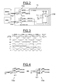
figure 2 illustrates more in details but still diagrammatically an example of a cell incorporated in a RF DAC block according to the invention ; -
figure 3 illustrates timing diagrams of signals related to the embodiment offigure 2 ; -
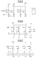
figures 4-7 illustrate diagrammatically examples of different elements of a cell according to the invention; -
figure 8 illustrates another embodiment of a RF DAC block according to the invention ; -
figure 9 illustrates diagrammatically a flow chart related to an embodiment of a method according to the invention ; -
figure 10 illustrates an example of a device according to another embodiment of the present invention ; -
figure 11 illustrates two notches resulting from the notch filter illustrated infigure 10 ; -
figure 12 illustrates diagrammatically a flow chart corresponding to another example of a method according to the invention ; -
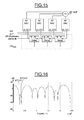
figures 13 to 18 illustrate diagrammatically other examples and embodiments of a device and a method according to the invention. -
Figure 1 illustrates diagrammatically an example of a transmission chain TX of a wireless apparatus WAP, such as a mobile phone. - The transmission chain comprises a digital stage DTX connected through a single radiofrequency digital to analog converter RDC, to an analog front end stage FE. The front end stage FE is connected to an antenna ANT.
- The digital stage DTX comprises low and high frequency digital logic, whose task is to change the sampling rate of the base-band (BB) signal delivered by a base-band processor, from Ffft (Base-Band Sampling Frequency, in the range of a few MHz) to Fc (Fcarrier) or a multiple of Fc, in the range of a few hundred MHz to a few GHz.
- This upsampled signal is then processed by a sigma-delta modulator (SDM) in order to represent the high resolution base-band signal using a reduced number of bits.
- The front end stage comprises conventionally a matching network, bandpass filter (BPF), balun, as well as a linear power amplifier (PA) and other conventional elements.
- The block RDC performs both the radiofrequency transposition and the digital to analog conversion.
- Further, the RF DAC block delivers the modulated radiofrequency analog signal at a desired power level, which is sufficient to drive the power amplifier PA.
- In this respect, the RF DAC block RDC receives the digital signal (sigma-delta modulated Baseband data) as well as the radiofrequency transposition signal ALT having the carrier frequency Fc and another control signal LO which has a frequency twice the carrier frequency.
- As it is usually the case in ZeroIF (direct conversion or intermediate frequency equal to zero) or lowIF (low intermediate frequency) transmitters, the control signal LO is delivered by a Phase Locked Loop (PLL). Thus, for example, a divider DV performing a frequency division by two is provided receiving the control signal LO and delivering the radiofrequency transposition signal ALT having the carrier frequency Fc.
- The radiofrequency digital to analog block RDC further receives a power control signal Bpwr delivered by the base band processor for adjusting the level of the radiofrequency modulated analog signal.
- As illustrated in
figure 2 , the digital signal delivered by the sigma-delta modulator SDM comprises conventionally the I channel and the Q channel. - Further, in this example, the digital signal delivered by the sigma-delta modulator SDM is a multibit digital signal. A cell is associated to one stream of bits (bi0, bq0) delivered by the sigma-delta modulator.
- The cell CL associated to the bit b0 (bi0, bq0) will be now disclosed more in details, bearing in mind that the other cells respectively associated to the other streams of bits bi are identical to the one which is now disclosed.
- The cell CL comprises first input means FIM which is also the block input means of the block RDC.
- The cell comprises transposition means TRM which receive the digital signal and delivers a digital transposed signals DIP0, DIM0, DQP0, DQM0 at the carrier frequency Fc which is also the frequency of the radiofrequency transposition signals ALTi, ALTq.
- The digital transposed signal is then converted into a radiofrequency analog signal OPO, OMO in digital to analog conversion means CVM which are controlled by the control signal LO and the power control signal Bpwr.
- The output means OP, OM form here the cell output means but also the RF block output means when only one cell is provided.
- Further, for example, both cell output means OP, OM are connected to the supply voltage through a load and to the power amplifier PA through the other conventional elements of the front end module.
- The structure disclosed here is a differential structure but the invention is of course not limited to such a structure.
- The operation of the cell CL is illustrated with the timing diagrams of
figure 3 . - More precisely, the output bit bi0 coming from the I channel and its inverted signal, are connected through two switches of the transposition means TRM to the DIP and DIM data inputs of the conversion means CVM.
- The switches of the transposition means are controllably commuted by the ALT signal to perform a digital mixing function between the Baseband digital signal delivered by the sigma-delta modulator and the radiofrequency transposition signal ALT.
- As indicated above, the radiofrequency transposition signal is obtained by dividing the control signal LO by two. Further, each transition of the radiofrequency transposition signal ALT occurs between two consecutive pulses of the control signal LO.
- A solution for obtaining such a result consists in using a divider DV having a phase shift such that the radiofrequency transposition signal ALT has a phase shift with respect to the control signal LO being smaller than the half of the period of the control signal LO.
- The resulting analog radiofrequency signal OUT0diff (or BBI x LOI) is the difference OPO-OMO at the cell output OP, OM. The corresponding signal from the Q channel is shown in dotted line (BBQ x LOQ).
- Controlling the digital to analog conversion by using the control signal LO does not modify the frequency transposition but reduces the phase noise of the signal, thus improving the quality of the digital transposed signal DIP, DIM, DQP, DQM. Further, when several cells are connected to the output of the sigma-delta modulator SDM, all the cells are controlled by the same control signal LO. Thus, a good synchronization between the several cells is provided.
- Further, the control power signal Bpwr permits to adjust the level of the radiofrequency analog signal at the desired level.
- The
elementary processing 90, performed by the cell CL is illustrated infigure 9 and comprises, as indicated above, aradiofrequency transposition 900 using the radiofrequency transposition signal ALT followed by a digital toanalog conversion 901 controlled by the control signal LO and the power control signal Bpwr. - Several solutions exist for implementing the transposition means TRM (mixing means).
- One solution is depicted diagrammatically in
figure 4 . In this figure, the switches are realized by XOR and XNOR gates as shown in the right part offigure 4 . - Turning now more particularly to
figure 5 , it can be seen that the digital to analog conversion means CVM may be implemented using global switching means GSWM controlled by the control signal LO and the digital transposed signal DIP, DIM, DQP, DQM. - These global switching means GSWM are connected to a current source SC controlled by the power control signal Bpwr and allow to deliver level-controlled current pulses at the cell output.
-
Figures 6 and 7 depict two possible circuit implementations of the conversion means CVM, using CMOS technology. - The first one (
figure 6 ) is using first switching means SW1 (for example MOS transistors) controlled by the control signal LOI, LOQ, and second switching means SW2 (MOS transistors) controlled by the digital transposed signal DIP, DIM, DQP, DQM. - These two switching means SW1 and SW2 are connected in series to thus combine the data and LO signals in the same way as it is described in
figure 5 . - The advantage of this solution is that the phase noise of the modulated radiofrequency analog signal is determined by the LO phase noise only. The contribution of the cell is negligible.
- A second solution is depicted in
figure 7 . - In this solution, only one MOS transistor MT per current switch is used, which is driven by a logic circuit LC (including here gate and inverter) that combines the data and LO signals.
- This switch is smaller than the ones used in the first solution depicted in
figure 6 and thus needs less driver power. - On these two solutions, other MOS transistors MSP are connected between the switching means and the cell output and are driven by the power control signal Bpwr such that, depending on the value of the power control signal, more or less current is delivered at the cell output.
- As illustrated in
figure 8 and explained above, the digital to analog conversion block RDC comprises several cells CL1-CLn adapted to respectively process the several parallel streams of bits of the multi-bits signal delivered by the sigma-delta modulator SDM. - The cell output means OP, OM of the several cells are respectively mutually coupled and form the block output means.
- Thus, the RF modulated analog signal delivered from the RF block RDC is obtained from the several cell analog signal respectively delivered by the several cells. In the present example all the cell analog signals (currents) are summed.
- Further, the several second (ALT), third (LO), (Bpwr) input means of the several cells are also mutually coupled.
- Further, depending on the "weight" of the bit of the digital word delivered by the sigma-delta modulator, the cell may have also a corresponding "weight".
- For example, as illustrated in
figure 8 , for a LSB (Least Significant Bit) a cell having a "weight" equal to 1 (i.e. a cell as the one disclosed above) may be used. For a MSB (Most Significant Bit) a cell CLn having a "weight" equal to 8 may be used. In this respect, such cell may be realized by connecting 8 conversion means CVM in parallel. - The examples illustrated in
figures 10 and following will permit to realize a notch filter allowing to place the notches around a desired band (for example the DCS, PCS or W-CDMA receive band), in order to reduce the filtering requirements of the transmission chain TX. - The example illustrated in
figure 10 comprises in the transmitting chain Tx of the wireless apparatus WAP, instead of one RF DAC (block RDC), two identical RF DACs RDC1 and RDC2, both receiving the control signal LO at their LO input (second input means), and the radiofrequency transposition signal ALT at their third input means. - A delay block DM is connected between the two data inputs of the
RF DACs RDC 1 and RDC2. - This delay block DM is clocked by the clock signal CKsdm with which the sigma-delta modulator is operated. The value of the delay is a multiple of the clock period Tck of the clock signal CKsdm. In the present case, the value of the multiple is equal to 5.
- Whereas the data input of the first RF DAC RDC1 is directly connected to the output of the sigma-delta modulator SDM, the data input of the second RF DAC RDC2 is connected to the output of the sigma-delta-modulator SDM through the delay block DM.
- The two RF DACs RDC1 and RDC2 respectively deliver two radiofrequency analog signals ARFS1 and ARFS2, which are summed in summation means SM in order to deliver a summed analog signal RF OUT which is delivered to the front end module FE.
- The summation is here a summation in current.
- The operation of the device illustrated in
figure 10 is depicted infigure 12 . - The sigma-delta modulated signal is delayed (step 40) in the delay block DM and both the sigma-delta modulated signal and the delayed signal are processed in the two RF DACs blocks RDC1 and RDC2 (step 41).
- The elementary processing 9 (step 41) is identical for both signals, and has been depicted in
figure 9 . - The frequency of the notch of the notch filter in the Baseband is related to the delay's value of the delay block. More precisely, the frequency of the notch in the Baseband is equal to Fck/2n, where Fck designates the frequency of the clock signal CKsdm and n designates the value of the multiple used in said delay block. In the present case, n is equal to 5.
- After frequency transposition to the carrier frequency Fc, the summed radiofrequency analog signal RF OUT (step 42) comprises two notches having respectively the frequencies Fc-f0 and Fc+f0, where f0 is the frequency of the notch in the Baseband.
- In the present example, the circuit of
figure 10 is designed to operate using for example a 802.11 g (WiFi) baseband signal as input. The modulation is for example a 64 QAM OFDM. The carrier frequency is equal to 2,4 GHz and the Phase Locked Loop (PLL) and the high speed logic operate at a frequency equal to twice the carrier frequency, i.e. to 4,8 GHz. - Thus, after frequency transposition, the signal comprises two notches NTCH1 et NTCH2 (
figure 11 ), respectively placed at 1,92 and 2,88 GHz. For the present application only the first notch NTCH1 is useful, as it is placed near the PCS receive band. - In order to avoid too much ripple in the radiofrequency analog output signal RF OUT, it is preferable that the notches are placed as for as possible from the carrier frequency.
- This can be obtained by adjusting the value of the delay, so that this value is smaller than 1/(30*BW), where BW is the frequency bandwidth of the summed radiofrequency analog signal RF OUT (
figure 11 ). - However, this threshold is only indicative and the man skilled in the art would be able to adjust it depending on the application.
- Generally speaking, the notch filter may comprise N identical radiofrequency digital to analog conversion blocks, N being greater than or equal to 2, and the digital delay means may thus include a chain of N-1 delay blocks respectively connected between the N data inputs of the radiofrequency digital to analog conversion blocks.
- Such an embodiment is illustrated in
figure 13 , where m RF DAC blocks RDC1-RDCm are illustrated, using delay means DM including a chain of m-1 delay blocks. - Each RF DAC block RDCi delivers a radiofrequency analog signal ARFSi.
- The operation of such an embodiment is illustrated diagrammatically in
figure 14 . - The delta-sigma modulated signal is successively delayed in the delay blocks (step 40) and the delta-sigma modulated signal and all delayed signals are processed (step 41) by using said identical
elementary processing 9 illustrated and disclosed infigure 9 . - All the radiofrequency analog signals ARFSi are summed in the summation means (step 82) in order to obtain the summed radiofrequency analog signal RF OUT.
- An example of such a notch filter is illustrated in
figure 15 , using four RF DAC blocks and three delay blocks having respectively delays values equal to 7Tck, 2Tck and 7Tck. The filter transfer function of this notch filter in baseband is illustrated infigure 16 and comprises two notches NTCH1 and NTCH2 around 280 and 340 MHz, as well as the other notches which are replicas of these two notches. - The carrier frequency is equal to 2,45 GHz in this example. The transfer function is transposed around the carrier frequency as shown in
figure 17 and the two notches are now placed around 2,1 and 2,2 GHz, i.e. around the WCDMA receiving band (figure 18 ), thus reducing the filter requirements from 70 to 40 dBs in this band. - It is also particularly advantageous that the values of the delays may be programmable, so that it is possible to place the notches within the WCDMA receiving band or the PCS receiving band or the DCS receiving band depending on the application.
Claims (18)
- Electronic device, comprising a radiofrequency digital to analog conversion block (RDC) having block input means (FIM) adapted to receive a digital signal containing at least one stream of successive bits and block output means adapted to deliver a radiofrequency analog signal, said block including at least one cell (CL) having first input means (FIM) coupled to said block input means, second input means adapted to receive a radiofrequency transposition signal (ALT), third input means adapted to receive a control signal (LO) having a frequency twice the frequency of the radiofrequency transposition signal, each transition of the radiofrequency transposition signal (ALT) occurring between two consecutive pulses of said control signal (LO), fourth input means adapted to receive a power control signal (Bpwr), cell output means (OP, OM) coupled to said block output means, transposition means (TRM) connected to said first input means and to said second input means and adapted to perform a radiofrequency transposition of said digital signal, and conversion means (CVM) controllable by said control signal (LO) and said power control signal (Bpwr) and adapted to receive said transposed digital signal and to perform a digital to analog conversion thereof for delivering a cell radiofrequency analog signal, said radiofrequency signal being obtained from said cell radiofrequency signal.
- Electronic device according to claim 1, further comprising generation means (PLL) adapted to deliver said control signal, and a frequency divider (DV) adapted to receive said control signal and to deliver said radiofrequency transposition signal having a delay with respect to said control signal, said delay being smaller than the half of the period of said control signal.
- Electronic device according to claim 1 or 2, wherein said conversion means (CVM) comprises first switching means (SW1) adapted to be controlled by said control signal, and second switching means (SW2) adapted to be controlled by said transposed digital signal.
- Electronic device according to claim 1 or 2, wherein said conversion means (CVM) comprises a logic circuit (LC) adapted to receive said control signal and said transposed digital signal and to deliver a combined control signal, and switching means (MT) controlled by said combined control signal.
- Electronic device according to any one of the preceding claims, wherein said transposition means (TRM) comprises mixing means controlled by said radiofrequency transposition signal.
- Electronic device according to any one of the preceding claims, wherein said digital signal contains several parallel streams of bits and said radiofrequency digital to analog conversion block includes several cells (CL1-CLn) adapted to respectively receive the several parallel streams of bits, the several second, third, fourth input means and the several cell output means of the several cells being respectively mutually coupled, said block output means being coupled to the several cell output means, said radiofrequency analog signal being obtained from the several cell radiofrequency analog signals.
- Electronic device according to any one of the preceding claims, wherein at least one cell (CLn) comprises several conversion means connected in parallel.
- Electronic device according to any one of the preceding claims, further comprising sigma-delta modulation means (SDM) having output means adapted to deliver said digital data signal.
- Electronic device, according to claim 8, wherein said sigma-delta modulation means (SDM) is adapted to operate with a clock signal, and said device further comprises a notch filter including at least two identical radiofrequency digital to analog conversion blocks (RDCi), digital delay means (DM) controlled by said clock signal and including a delay block connected between the two first input means, the frequency of a notch of said notch filter being related to the delay's value of the delay block, and summation means (SM) adapted to sum said radiofrequency analog signals (ARFSi).
- Electronic device according to claim 9, wherein said notch filter comprises N identical radiofrequency digital to analog conversion blocks, N being greater than or equal to 2, and said digital delay means (DM) includes a chain of N-1 delay blocks respectively connected between the N first input means.
- Electronic device according to claim 9 or 10, wherein the delay's value of the delay means is smaller than (1/(30*BW)), where BW is the frequency band width of the radiofrequency analog signal.
- Electronic device according to any one of the claims 9 to 11, wherein the delay means are programmable.
- Electronic device according to any one of the preceding claims, realized within an integrated circuit.
- Wireless apparatus, including an electronic device according to any one of the preceding claims.
- Method for processing a digital signal, comprising an elementary processing (9) including a radiofrequency transposition (900) with a radiofrequency transposition signal and a digital to analog conversion (901) of said transposed digital signal for delivering a radiofrequency analog signal, said digital to analog conversion being controlled by a control signal and a power control signal, said control signal having a frequency twice the frequency of the radiofrequency transposition signal, each transition of the radiofrequency transposition signal occurring between two consecutive pulses of said control signal.
- Method according to claim 15, wherein said digital signal is delivered by sigma-delta modulation means operating with a clock signal, and further comprising delaying (40) said digital signal using said clock signal for obtaining at least one delayed digital signal, the frequency of a notch of said notch filter being related to the delay's value, processing (41) said digital signal and said delayed digital signal with said elementary processing (9) and summing (42) all said radiofrequency analog signals.
- Method according to claim 16, wherein delaying said digital signal comprises successively delaying (40) said digital signal with several respective delays for obtaining at least two different delayed signals, processing (41) said digital signal and all said delayed signal with said elementary processing (9), and summing (82) all said radiofrequency analog signals.
- Method according to claim 7 or 8, wherein each delay's value is programmable.
Priority Applications (2)
| Application Number | Priority Date | Filing Date | Title |
|---|---|---|---|
| EP07301366A EP2037584A1 (en) | 2007-09-14 | 2007-09-14 | Method for performing a digital to analog conversion of a digital signal, and corresponding electronic device. |
| US12/208,966 US7755524B2 (en) | 2007-09-14 | 2008-09-11 | Method for performing a digital to analog conversion of a digital signal, and corresponding electronic device |
Applications Claiming Priority (1)
| Application Number | Priority Date | Filing Date | Title |
|---|---|---|---|
| EP07301366A EP2037584A1 (en) | 2007-09-14 | 2007-09-14 | Method for performing a digital to analog conversion of a digital signal, and corresponding electronic device. |
Publications (1)
| Publication Number | Publication Date |
|---|---|
| EP2037584A1 true EP2037584A1 (en) | 2009-03-18 |
Family
ID=38925482
Family Applications (1)
| Application Number | Title | Priority Date | Filing Date |
|---|---|---|---|
| EP07301366A Withdrawn EP2037584A1 (en) | 2007-09-14 | 2007-09-14 | Method for performing a digital to analog conversion of a digital signal, and corresponding electronic device. |
Country Status (2)
| Country | Link |
|---|---|
| US (1) | US7755524B2 (en) |
| EP (1) | EP2037584A1 (en) |
Cited By (3)
| Publication number | Priority date | Publication date | Assignee | Title |
|---|---|---|---|---|
| US7755524B2 (en) * | 2007-09-14 | 2010-07-13 | Stmicroelectronics N.V. | Method for performing a digital to analog conversion of a digital signal, and corresponding electronic device |
| EP2328273A1 (en) * | 2009-11-26 | 2011-06-01 | Nxp B.V. | Digital radio frequency modulators |
| EP2541776A1 (en) * | 2011-06-29 | 2013-01-02 | Imec | Radio frequency modulators |
Families Citing this family (6)
| Publication number | Priority date | Publication date | Assignee | Title |
|---|---|---|---|---|
| EP3678294B1 (en) * | 2007-09-14 | 2022-02-02 | Telefonaktiebolaget LM Ericsson (publ) | Method for notch filtering a digital signal, and corresponding electronic device |
| EP2266203B1 (en) * | 2008-04-18 | 2012-05-23 | STMicroelectronics SA | Integrated circuit and corresponding method of processing a multitype radio frequency digital signal |
| KR100960022B1 (en) * | 2008-08-22 | 2010-05-28 | 전자부품연구원 | Digital Intermediate Frequency Radio Transmitter, High Frequency Modulation Device and Method |
| DE102009024284A1 (en) * | 2009-06-05 | 2010-12-09 | Rheinisch-Westfälische Technische Hochschule Aachen | Digital RF modulator with sigma-delta based notch filter |
| US10587354B1 (en) * | 2018-11-26 | 2020-03-10 | Intel Corporation | Multiphase transmitter digital front end |
| US12592728B2 (en) * | 2022-08-30 | 2026-03-31 | Apple Inc. | Digital-to-analog converter with localized frequency multiplication circuits |
Citations (1)
| Publication number | Priority date | Publication date | Assignee | Title |
|---|---|---|---|---|
| WO2006117590A1 (en) * | 2005-04-29 | 2006-11-09 | Nokia Corporation | Polar transmitter with digital to rf converter |
Family Cites Families (9)
| Publication number | Priority date | Publication date | Assignee | Title |
|---|---|---|---|---|
| GB9422683D0 (en) | 1994-11-10 | 1995-01-04 | At & T Wireless Communicat | RF transmitter |
| KR100457175B1 (en) * | 2002-12-14 | 2004-11-16 | 한국전자통신연구원 | Quadrature modulation transmitter |
| US7116253B2 (en) * | 2003-08-05 | 2006-10-03 | Stmicroelectronics N.V. | Radio frequency digital-to-analog converter |
| WO2005015752A2 (en) | 2003-08-05 | 2005-02-17 | Stmicroelectronics, Inc. | Noise shaped interpolator and decimator apparatus and method |
| US6952177B1 (en) * | 2004-03-08 | 2005-10-04 | The Boeing Company | Traveling wave, multiplying D/A converter |
| US7236112B2 (en) | 2005-01-21 | 2007-06-26 | Technoconcepts, Inc. | Self-tuning output digital filter for direct conversion delta-sigma transmitter |
| US7528754B1 (en) * | 2006-02-09 | 2009-05-05 | Arizona Board Of Regents | Finite impulse response digital to analog converter |
| US7317412B2 (en) * | 2006-05-15 | 2008-01-08 | M/A-Com, Inc. | Techniques for biasing a radio frequency digital to analog converter |
| EP2037584A1 (en) * | 2007-09-14 | 2009-03-18 | STMicroelectronics N.V. | Method for performing a digital to analog conversion of a digital signal, and corresponding electronic device. |
-
2007
- 2007-09-14 EP EP07301366A patent/EP2037584A1/en not_active Withdrawn
-
2008
- 2008-09-11 US US12/208,966 patent/US7755524B2/en active Active
Patent Citations (1)
| Publication number | Priority date | Publication date | Assignee | Title |
|---|---|---|---|---|
| WO2006117590A1 (en) * | 2005-04-29 | 2006-11-09 | Nokia Corporation | Polar transmitter with digital to rf converter |
Non-Patent Citations (1)
| Title |
|---|
| LEE H-S ET AL: "Radio Frequency Digital-to-Analog Converter", IEEE JOURNAL OF SOLID-STATE CIRCUITS, IEEE SERVICE CENTER, PISCATAWAY, NJ, US, vol. 39, no. 9, September 2004 (2004-09-01), pages 1462 - 1467, XP011117965, ISSN: 0018-9200 * |
Cited By (3)
| Publication number | Priority date | Publication date | Assignee | Title |
|---|---|---|---|---|
| US7755524B2 (en) * | 2007-09-14 | 2010-07-13 | Stmicroelectronics N.V. | Method for performing a digital to analog conversion of a digital signal, and corresponding electronic device |
| EP2328273A1 (en) * | 2009-11-26 | 2011-06-01 | Nxp B.V. | Digital radio frequency modulators |
| EP2541776A1 (en) * | 2011-06-29 | 2013-01-02 | Imec | Radio frequency modulators |
Also Published As
| Publication number | Publication date |
|---|---|
| US20090073013A1 (en) | 2009-03-19 |
| US7755524B2 (en) | 2010-07-13 |
Similar Documents
| Publication | Publication Date | Title |
|---|---|---|
| EP3678294B1 (en) | Method for notch filtering a digital signal, and corresponding electronic device | |
| US7755524B2 (en) | Method for performing a digital to analog conversion of a digital signal, and corresponding electronic device | |
| Eloranta et al. | A Multimode Transmitter in 0.13$\mu\hbox {m} $ CMOS Using Direct-Digital RF Modulator | |
| EP2097984B1 (en) | Digital linear transmitter architecture | |
| US7061989B2 (en) | Fully digital transmitter including a digital band-pass sigma-delta modulator | |
| US5557642A (en) | Direct conversion receiver for multiple protocols | |
| US8417750B2 (en) | Filters for communication systems | |
| US8542773B2 (en) | Digital RF converter, digital RF modulator and transmitter including the same | |
| US7548180B2 (en) | Method and system for digital to analog conversion for power amplifier driver amplitude modulation | |
| US20050118977A1 (en) | Method, apparatus, and systems for digital radio communication systems | |
| WO2007117761A2 (en) | Rf transmitter with interleaved iq modulation | |
| EP2266208A2 (en) | Output stage for a digital rf transmitter, method for providing an rf output signal in a digital rf transmitter, and digital rf transmitter | |
| EP1349284B1 (en) | Apparatus and methods for digital-to-analog conversion | |
| EP1925094A1 (en) | Multi-band radio frequency modulator | |
| US7310386B2 (en) | Radio receiver utilizing a single analog to digital converter | |
| US6888485B2 (en) | Digital-analog converter | |
| KR101292667B1 (en) | Digital RF converter and digital RF modulator and transmitter including the same | |
| Strasser et al. | Reconfigurable mixed-signal single-chip transmitter for multistandard-terminals | |
| Frappé et al. | Multimode transmitters with ΔΣ-based all-digital RF signal generation | |
| Frappé | Digital radio frequency signal generation towards ultimate transmitters | |
| KR20050116304A (en) | Direct conversion delta-sigma receiver |
Legal Events
| Date | Code | Title | Description |
|---|---|---|---|
| PUAI | Public reference made under article 153(3) epc to a published international application that has entered the european phase |
Free format text: ORIGINAL CODE: 0009012 |
|
| AK | Designated contracting states |
Kind code of ref document: A1 Designated state(s): AT BE BG CH CY CZ DE DK EE ES FI FR GB GR HU IE IS IT LI LT LU LV MC MT NL PL PT RO SE SI SK TR |
|
| AX | Request for extension of the european patent |
Extension state: AL BA HR MK RS |
|
| 17P | Request for examination filed |
Effective date: 20090915 |
|
| 17Q | First examination report despatched |
Effective date: 20091008 |
|
| AKX | Designation fees paid |
Designated state(s): DE FR GB |
|
| STAA | Information on the status of an ep patent application or granted ep patent |
Free format text: STATUS: THE APPLICATION IS DEEMED TO BE WITHDRAWN |
|
| 18D | Application deemed to be withdrawn |
Effective date: 20150401 |