EP2037575A1 - Micromechanical resonator - Google Patents
Micromechanical resonator Download PDFInfo
- Publication number
- EP2037575A1 EP2037575A1 EP07116580A EP07116580A EP2037575A1 EP 2037575 A1 EP2037575 A1 EP 2037575A1 EP 07116580 A EP07116580 A EP 07116580A EP 07116580 A EP07116580 A EP 07116580A EP 2037575 A1 EP2037575 A1 EP 2037575A1
- Authority
- EP
- European Patent Office
- Prior art keywords
- layer
- resonator
- electrode
- semiconductor
- depositing
- Prior art date
- Legal status (The legal status is an assumption and is not a legal conclusion. Google has not performed a legal analysis and makes no representation as to the accuracy of the status listed.)
- Withdrawn
Links
- 239000004065 semiconductor Substances 0.000 claims abstract description 84
- 239000000758 substrate Substances 0.000 claims abstract description 62
- 238000002955 isolation Methods 0.000 claims abstract description 57
- 238000000151 deposition Methods 0.000 claims abstract description 30
- 230000003071 parasitic effect Effects 0.000 claims abstract description 15
- 238000004519 manufacturing process Methods 0.000 claims abstract description 10
- 238000000034 method Methods 0.000 claims description 23
- 238000000926 separation method Methods 0.000 description 11
- 238000005229 chemical vapour deposition Methods 0.000 description 8
- 239000000463 material Substances 0.000 description 8
- VYPSYNLAJGMNEJ-UHFFFAOYSA-N silicon dioxide Inorganic materials O=[Si]=O VYPSYNLAJGMNEJ-UHFFFAOYSA-N 0.000 description 8
- XUIMIQQOPSSXEZ-UHFFFAOYSA-N Silicon Chemical compound [Si] XUIMIQQOPSSXEZ-UHFFFAOYSA-N 0.000 description 7
- 238000009792 diffusion process Methods 0.000 description 7
- 229910052710 silicon Inorganic materials 0.000 description 7
- 239000010703 silicon Substances 0.000 description 7
- 229910052814 silicon oxide Inorganic materials 0.000 description 6
- 239000013078 crystal Substances 0.000 description 5
- 229910021420 polycrystalline silicon Inorganic materials 0.000 description 5
- 239000012535 impurity Substances 0.000 description 4
- 229910052751 metal Inorganic materials 0.000 description 4
- 239000002184 metal Substances 0.000 description 4
- RYGMFSIKBFXOCR-UHFFFAOYSA-N Copper Chemical compound [Cu] RYGMFSIKBFXOCR-UHFFFAOYSA-N 0.000 description 3
- 239000004411 aluminium Substances 0.000 description 3
- 229910052782 aluminium Inorganic materials 0.000 description 3
- XAGFODPZIPBFFR-UHFFFAOYSA-N aluminium Chemical compound [Al] XAGFODPZIPBFFR-UHFFFAOYSA-N 0.000 description 3
- 229910052802 copper Inorganic materials 0.000 description 3
- 239000010949 copper Substances 0.000 description 3
- 230000008878 coupling Effects 0.000 description 3
- 238000010168 coupling process Methods 0.000 description 3
- 238000005859 coupling reaction Methods 0.000 description 3
- 229910021421 monocrystalline silicon Inorganic materials 0.000 description 3
- JBRZTFJDHDCESZ-UHFFFAOYSA-N AsGa Chemical compound [As]#[Ga] JBRZTFJDHDCESZ-UHFFFAOYSA-N 0.000 description 2
- GPXJNWSHGFTCBW-UHFFFAOYSA-N Indium phosphide Chemical compound [In]#P GPXJNWSHGFTCBW-UHFFFAOYSA-N 0.000 description 2
- 229910052581 Si3N4 Inorganic materials 0.000 description 2
- 238000005530 etching Methods 0.000 description 2
- 229910052732 germanium Inorganic materials 0.000 description 2
- GNPVGFCGXDBREM-UHFFFAOYSA-N germanium atom Chemical compound [Ge] GNPVGFCGXDBREM-UHFFFAOYSA-N 0.000 description 2
- 238000003780 insertion Methods 0.000 description 2
- 230000037431 insertion Effects 0.000 description 2
- 238000005468 ion implantation Methods 0.000 description 2
- 150000002739 metals Chemical class 0.000 description 2
- 230000010287 polarization Effects 0.000 description 2
- 239000010453 quartz Substances 0.000 description 2
- HQVNEWCFYHHQES-UHFFFAOYSA-N silicon nitride Chemical compound N12[Si]34N5[Si]62N3[Si]51N64 HQVNEWCFYHHQES-UHFFFAOYSA-N 0.000 description 2
- 230000001808 coupling effect Effects 0.000 description 1
- 230000001419 dependent effect Effects 0.000 description 1
- 230000008021 deposition Effects 0.000 description 1
- 238000009795 derivation Methods 0.000 description 1
- 230000000694 effects Effects 0.000 description 1
- 230000010354 integration Effects 0.000 description 1
- 238000001228 spectrum Methods 0.000 description 1
- 235000012431 wafers Nutrition 0.000 description 1
Images


Classifications
-
- H—ELECTRICITY
- H03—ELECTRONIC CIRCUITRY
- H03H—IMPEDANCE NETWORKS, e.g. RESONANT CIRCUITS; RESONATORS
- H03H3/00—Apparatus or processes specially adapted for the manufacture of impedance networks, resonating circuits, resonators
- H03H3/007—Apparatus or processes specially adapted for the manufacture of impedance networks, resonating circuits, resonators for the manufacture of electromechanical resonators or networks
- H03H3/0072—Apparatus or processes specially adapted for the manufacture of impedance networks, resonating circuits, resonators for the manufacture of electromechanical resonators or networks of microelectro-mechanical resonators or networks
-
- H—ELECTRICITY
- H03—ELECTRONIC CIRCUITRY
- H03H—IMPEDANCE NETWORKS, e.g. RESONANT CIRCUITS; RESONATORS
- H03H9/00—Networks comprising electromechanical or electro-acoustic elements; Electromechanical resonators
- H03H9/02—Details
- H03H9/02244—Details of microelectro-mechanical resonators
- H03H9/02433—Means for compensation or elimination of undesired effects
-
- H—ELECTRICITY
- H03—ELECTRONIC CIRCUITRY
- H03H—IMPEDANCE NETWORKS, e.g. RESONANT CIRCUITS; RESONATORS
- H03H9/00—Networks comprising electromechanical or electro-acoustic elements; Electromechanical resonators
- H03H9/24—Constructional features of resonators of material which is not piezoelectric, electrostrictive, or magnetostrictive
- H03H9/2405—Constructional features of resonators of material which is not piezoelectric, electrostrictive, or magnetostrictive of microelectro-mechanical resonators
- H03H9/2447—Beam resonators
- H03H9/2457—Clamped-free beam resonators
-
- H—ELECTRICITY
- H03—ELECTRONIC CIRCUITRY
- H03H—IMPEDANCE NETWORKS, e.g. RESONANT CIRCUITS; RESONATORS
- H03H9/00—Networks comprising electromechanical or electro-acoustic elements; Electromechanical resonators
- H03H9/24—Constructional features of resonators of material which is not piezoelectric, electrostrictive, or magnetostrictive
- H03H9/2405—Constructional features of resonators of material which is not piezoelectric, electrostrictive, or magnetostrictive of microelectro-mechanical resonators
- H03H9/2447—Beam resonators
- H03H9/2463—Clamped-clamped beam resonators
-
- H—ELECTRICITY
- H03—ELECTRONIC CIRCUITRY
- H03H—IMPEDANCE NETWORKS, e.g. RESONANT CIRCUITS; RESONATORS
- H03H9/00—Networks comprising electromechanical or electro-acoustic elements; Electromechanical resonators
- H03H9/02—Details
- H03H9/02244—Details of microelectro-mechanical resonators
- H03H9/02433—Means for compensation or elimination of undesired effects
- H03H2009/02456—Parasitic elements or effects, e.g. parasitic capacitive coupling between input and output
-
- H—ELECTRICITY
- H03—ELECTRONIC CIRCUITRY
- H03H—IMPEDANCE NETWORKS, e.g. RESONANT CIRCUITS; RESONATORS
- H03H9/00—Networks comprising electromechanical or electro-acoustic elements; Electromechanical resonators
- H03H9/02—Details
- H03H9/02244—Details of microelectro-mechanical resonators
- H03H2009/02488—Vibration modes
- H03H2009/02511—Vertical, i.e. perpendicular to the substrate plane
Definitions
- the present invention relates to resonators, and more particularly, to micromechanical resonators.
- Crystal resonators are electronic circuits that use the mechanical resonance of a vibrating crystal of piezoelectric material to create an electrical signal with a very precise frequency. This frequency is commonly used to keep track of time, to provide a stable clock signal for digital integrated circuits, and to stabilize frequencies for radio transmitters.
- quartz crystal resonators have been used in spread spectrum, radio frequency and wireless applications.
- crystal resonators have problems of compatibility with semiconductors' fabrication processes.
- micromechanical resonators Unlike quartz crystal resonators, micromechanical ones are excellent candidates for integration within a semiconductor substrate, due to its compatibility with the semiconductors' fabrication process.
- micromechanical resonators built on semiconductor wafers present some embedded parasitic components, such as resonator to substrate capacitance, series resistance, etc. These parasitic components reduce the electrical performance (Q-factor, insertion loss, etc.) of the resonators.
- the coupling of high frequency signals through the semiconductor substrate underneath a micromechanical resonator causes severe problems.
- this coupling allows signals to pass through the substrate, thereby reducing the signal amplitude through the resonator.
- the resonator performance is thus reduced by this coupling effect.
- a method of manufacturing a micromechanical resonator which comprises the steps of: depositing a first semiconductor layer on a semiconductor substrate, wherein the doping type of this first semiconductor layer is the opposite of the doping type of the semiconductor substrate; depositing a first dielectric layer on that first semiconductor layer; depositing a first electrode layer and a second electrode layer on the first dielectric layer, the electrode layers corresponding to the electrodes of a micromechanical resonator; depositing a second dielectric layer configured for creating a resonator gap after removing that second dielectric layer; depositing a structure layer, which corresponds to the structure of a micromechanical resonator.
- the method further comprises the step of, after depositing that first semiconductor layer and before depositing that first dielectric layer, depositing an electrical isolation layer on a portion of the first semiconductor layer, for reducing the parasitic effect caused by an electric path created between the electrodes of the resonator and the substrate.
- the doping type of the electrical isolation layer is the opposite of the doping type of the first semiconductor layer.
- a step of depositing a highly concentrated doping layer on the semiconductor substrate is done, the doping type of the highly concentrated doping layer being the opposite of the doping type of the semiconductor substrate.
- the electrical isolation layer which is deposited on a portion of the first semiconductor layer has a cross-sectional length smaller than the cross-sectional distance between a first end of a first electrode and a second end of a second electrode of the resonator, these first and second ends being facing.
- the first end of the first electrode is the end of the first electrode which is closest to the end of the second electrode which is closest to the first electrode.
- That portion of the first semiconductor layer on which that electrical isolation layer is deposited further extends along an area above which at least a whole one of those electrodes is designed to be deposited.
- the invention also refers to a micromechanical resonator which comprises: a semiconductor substrate having a doping type; a first semiconductor layer deposited on that semiconductor substrate, wherein the doping type of that first semiconductor layer is the opposite of the doping type of the semiconductor substrate; an electrical isolation layer deposited on the first semiconductor layer for reducing the parasitic effect caused by an electric path created between the electrodes of the resonator and the substrate; a first dielectric layer deposited on the electrical isolation layer and on the portion of the first semiconductor layer not covered by the electrical isolation layer; a first electrode layer and a second electrode layer deposited on the first dielectric layer, those electrode layers corresponding to the electrodes of the micromechanical resonator; a structure layer corresponding to the structure of the micromechanical resonator; a resonator gap located between the electrode layers and the structure layer.
- the doping type of the electrical isolation layer is the opposite of the doping type of the first semiconductor layer.
- the resonator further comprises a highly concentrated doping layer between the semiconductor substrate and the first semiconductor layer, the doping type of the highly concentrated doping layer being the opposite of the doping type of the semiconductor substrate.
- the electrical isolation layer which is placed on a portion of the first semiconductor layer has a cross-sectional length smaller than the cross-sectional distance between a first end of a first electrode and a second end of a second electrode of the resonator, these first and second ends being facing.
- the portion of the first semiconductor layer on which the electrical isolation layer is placed further extends underneath at least a whole one of the electrodes.
- a bridge type resonator having at least three electrodes and two electrical isolation layers is presented.
- the resonator further comprises electrical connections for providing input/output ports from/to other equipment to which the micromechanical resonator is configured to be connected.
- the term “highly” used in the expression “highly concentrated” refers to doping concentrations higher than about 10 14 cm -3 .
- sacrificial referred to a “sacrificial layer of a material” means that such a layer is etched in order to later release a resonator structure for mechanical vibration. Since during the fabrication process it is not possible to deposit or grow any structure on an air space, a “sacrificial" layer is required.
- a semiconductor substrate 1 has to be chosen.
- conventional semiconductor substrates are silicon substrates, such as p-type or n-type silicon substrates.
- Other examples of semiconductor substrates are those made of germanium (Ge), gallium arsenide (GaAs) and indium phosphorus (InP).
- Figure 2a shows a p-type silicon semiconductor substrate, but the invention should not be limited to p-type substrates.
- highly concentrated doping 2 can be added to the semiconductor substrate 1 in order to reduce resistivity of the next layer to be deposited, as will be explained later.
- Highly concentrated doping 2 is deposited by any conventional means, such as thermal diffusion, ion implantation, etc. If the semiconductor substrate 1 is of p-type, the doping 2 is of n-type, and vice versa.
- the doping 2 illustrated in figure 2b is n-type.
- a semiconductor layer 3 is deposited on the semiconductor substrate 1 and on the doping area 2, if this optional doping 2 has been deposited.
- Layer 3 is deposited or grown by any conventional means, such as thermal diffusion, chemical vapour deposition (CVD), epitaxial growth, etc. If the semiconductor substrate 1 is of p-type, layer 3 is of n-type, and vice versa. Layer 3 illustrated in figure 2c is n-type.
- Non-limiting examples of conventional semiconductor substrates are silicon substrates, germanium (Ge) substrates, gallium arsenide (GaAs) substrates and indium phosphorus (InP) substrates.
- doping area 2 is optional. Adding this doping area 2 is, however, recommended, since thanks to said highly concentrated doping area 2, the resistivity of layer 3 is reduced.
- This doping area 2 is of the same type as layer 3, but in a higher concentration. In accordance with the definition of "highly concentrated” already given, the doping concentration of this doping area 2 is about at least 10 times higher than that of semiconductor layer 3.
- a dielectric layer 5 is then deposited, as shown in figure 1 .
- the purpose of this dielectric layer 5 is to isolate the resonator from the substrate.
- the electrode layers 6 of the resonator are grown.
- a doping area or electrical isolation layer 4 whose type is the opposite one to the one of layer 3 is grown.
- doping area 4 is of p-type and vice versa.
- This doping area or electrical isolation layer 4 is deposited on semiconductor layer 3. This is illustrated in figure 2d , in which case doping area or electrical isolation layer 4 is a p-type one. Non-limiting examples of depositing this doping area or electrical isolation layer 4 are by thermal diffusion and ion implantation among others. In figure 2d , several doping areas 4 are deposited, because several resonators can be built on the same substrate.
- dielectric layer 5 is grown, covering all the surface of the already deposited materials, as shown in figure 2e .
- dielectric layer 5 covers the electrical isolation layer 4 and the parts of the semiconductor layer 3 not covered by these electrical isolation layer or layers 4.
- Non-limiting examples of dielectric layers are Silicon Oxide (SiO 2 ), silicon nitride and silicon oxynitride.
- dielectric layer 5 is made of silicon oxide.
- Dielectric 5 is deposited or grown by any conventional means, such as thermal diffusion, chemical vapour deposition (CVD), epitaxial growth, etc.
- first and second electrodes of the micromechanical resonator are created, for which a first electrode layer 6 and a second electrode layer 6' are deposited or grown.
- reference 10 represents the end of the first electrode layer 6 which is closest to the second electrode layer 6'
- reference 10' represents the end of the second electrode layer 6' which is closest to the first electrode layer 6.
- the two separate electrodes formed by layers 6 6' represent different electrical nodes, which form different ports of the resonator (input, output, etc.)
- Non-limiting examples of materials for creating an electrode layer are poly-Silicon, single crystal silicon and metal, such as aluminium or copper.
- deposited electrode layers 6 6' are made of poly-silicon. Pattern etching is then done.
- the cross-sectional distance d ele between the ends 10 and 10' of electrode layers 6 and 6' has to be a bit longer than the cross-sectional length d iso of doping area or electrical isolation layer 4.
- the doping area or electrical isolation layer 4 is a bit narrower d iso than the separation d ele between the ends 10 and 10' of electrode layers 6 and 6'.
- the reason why d iso has to be shorter than d ele is that it prevents the parasitic signal path to travel directly to the electrical isolation layer 4. If d ele ⁇ d iso , the isolation effect of the electrical isolation layer 4 does not work well. This is explained in detail with reference to figures 3b and 3c .
- the cross-sectional length d iso only needs to satisfy the above mentioned requirement of d iso ⁇ d ele .
- the minimum value of d iso is only limited by practical constraints, such as the equipment of deposition, thermal diffusion, etc. These constraints are out of the scope of the present invention.
- the minimum value of d ele is dependent on or defined by the pattern etching resolution of electrodes 10 and 10'.
- a sacrificial dielectric layer 7 for creating a resonator gap is deposited.
- dielectric layers are Silicon Oxide (SiO 2 ), silicon nitride and silicon oxynitride.
- dielectric layer 7 is made of silicon oxide.
- Dielectric layer 7 is deposited or grown by any conventional means, such as thermal diffusion, chemical vapour deposition (CVD), epitaxial growth, etc. This dielectric layer 7 is later removed and a gap remains. This gap or hole forms an electrical contact between the resonator's electrode layers 6 6' and the top layer or layers of the resonator structure, as will be shown later.
- This sacrificial dielectric layer 7 does not need to cover the whole surface of the electrode layers 6 6'.
- the amount of electrode layers 6 6', as well as the amount of the remaining dielectric layer 5 which is covered by the sacrificial dielectric layer 7 depends on the specific resonator's design and application.
- another layer 8 is deposited on part of the electrode layers 6 6' and on part of said sacrificial dielectric layer 7.
- This layer is the resonator structure layer 8 and is deposited or grown by any conventional means, such as thermal diffusion, chemical vapour deposition (CVD), epitaxial growth, etc.
- Non-limiting examples of materials for making such a structure are poly-Silicon, single crystal silicon and metals, such as aluminium or copper.
- Layer 8 of figure 2h is made of poly-silicon.
- This structure is resonant, that is, if an AC signal is applied between electrodes 6 and 6', the resonator formed by resonator layer 8 vibrates at the same frequency as the resonator's frequency of vibration of the normal mode (Eigen value), which is the resonance frequency.
- Eigen value the normal mode
- the amount of electrode layers 6 6', as well as the amount of the sacrificial dielectric layer 7 which is covered by the structure layer 8 depends on the specific resonator's design and application.
- the dielectric layer 7 i.e. sacrificial oxide
- the fabrication process is finished.
- Figure 3a illustrates the micromechanical resonator 30 obtained by the process described with reference to figures 2a-2i .
- Reference 9 represents the separation area achieved by the invention. This separation area 9 is limited, at its upper side, by the ends 10 10' of the resonator's electrodes 6 6', and at its bottom side, by doping area or electrical isolation layer 4.
- the purpose of the doping area or electrical isolation layer 4 is to isolate the ends 10 10' of resonant's electrodes or layers 6 6'. Without the doping area or electrical isolation layer 4 which creates the separation area 9, parasitic current flows between both ends of the electrode layers.
- Figure 1b shows a possible equivalent circuit of such a micromechanical resonator without doping area.
- Figure 1c shows an alternative, possible equivalent circuit of such a micromechanical resonator without doping area. The choice of one of the two possible equivalent circuits depends on the electrical characteristic of the materials used.
- Figure 3b shows the equivalent circuit of resonator 30 of the invention, in which d iso ⁇ d ele . Capacitances 11 and 11' create an open circuit, thus avoiding parasitic current to flow.
- Figure 3c represents the equivalent circuit of a similar resonator, which differs from the one of the present invention in that d iso > d ele . As can be noticed, in this the equivalent circuit parasitic signal path is not cut. This equivalent circuit is similar to that of figure 1b .
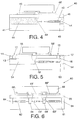
- Figure 4 shows an alternative embodiment of a micromechanical resonator 40 of the invention.
- semiconductor layer 43 is an n-type one.
- Reference 42 represents an optional doping layer similar to the one referred to as 2 in figure 2b .
- Reference 44 represents a doping area or electrical isolation layer thanks to which a separation area 49 is achieved.
- doping area or electrical isolation layer 44 is a p-type one. As can be seen, this doping area or electrical isolation layer 44 occupies a larger portion than doping layer 4 in figure 3a . In fact, doping area or electrical isolation layer 44 extends all beneath one 46 of the resonant's electrodes 46 46'.
- doping area or electrical isolation layer 44 creates an electrical separation area 49 between the ends of the electrodes and the doping area 44. At the other end of doping area or electrical isolation layer 44, this doping layer or electrical isolation layer 44 does not start exactly under the end of electrode layer 46', but a bit towards the end of the facing electrode 46, In other words, the projection of the end of the electrode layer 46' which is closest to the facing electrode layer 46 does not overlap with the beginning of the doping area or electrical isolation layer 44.
- the micromechanical resonator of the invention also comprises electrical connections, designed for providing input/output ports from/to other equipment.
- Figure 5 shows such electrical connections 12 15 comprised in the resonator 40 of figure 4 .
- Electrical connection 12 is deposited on a p-type area (doping area 54).
- electrical connection 12 requires a high-concentrated p-doping or impurity area 13, deposited or diffused on active p-type doping area 54, in order to make ohmic contact between buried layer 54 and interconnection layer 14.
- an interconnection area 14 is deposited on top of this high-concentrated p-doping area 13 deposited.
- interconnection area 14 is made of metal.
- Non-limiting examples of materials for interconnection layer 14 are metals, such as aluminium, copper, etc. and low resistive silicon layers, such as n/p-doped poly-crystalline silicon and single crystal silicon.
- electrical connection 15 is deposited on an n-type area (layer 53)
- electrical connection 15 requires a high-concentrated n-doping or impurity area 16, deposited on active n-type layer 53, in order to make ohmic contact between buried layer 53 and interconnection layer 17.
- an interconnection layer 17 is deposited on top of this high-concentrated n-doping area 16 deposited. Examples of interconnection layer 17 are the same ones as indicated for interconnection layer 14.
- FIG. 6 shows an example of a micromechanical resonator 60 of the invention.
- resonator 60 is a bridge type resonator.
- a highly concentrated doping 62 is deposited, and then a semiconductor layer 63 is grown.
- two doping areas or electrical isolation layers 64 64' whose type is the opposite one to the one of layer 63 are deposited.
- a dielectric layer 65 is grown, covering all the surface of the already deposited materials.
- three electrode layers 66 66' 66" are deposited.
- Left-handed and right-handed electrode layers 66 66" are the same node/terminal, that is to say, the same electrical node or electrical terminal which can be connected to a circuit, a signal source, a load, etc.
- Centered electrode layer 66' is of different node/terminal from electrode layer 66 66''.
- Each electrode layer 66 66' 66'' is separated by isolation from the adjacent one or ones by means of doping areas or electrical isolation layers 64 64', because doping area 64 creates an isolation or separation area 69' between the end of electrode layer 66 which is closest to electrode layer 66' and the end of electrode layer 66' which is closest to the said electrode layer 66 and said electrode layer 66.
- doping area 64' creates an isolation or separation area 69'' between the end of electrode layer 66' which is closest to right-handed electrode layer 66'' and the end of the right-handed electrode layer 66'' which is closest to electrode layer 66'.
- a sacrificial dielectric layer 67 for creating a resonator gap is deposited.
- a resonator structure 68 is added and the dielectric layer 67 is removed.
- Each electrode layer is thus separated by isolation or separation layers that are buried in substrate.
- a detail structure of bridge type resonator is described, for example, in European patent application EP1777815 , by this applicant.
- the polarization of impurities used in the following layer to be deposited is exchanged (to p-type).
- the polarization of impurities used in the following layer to be deposited is exchanged to n-type.
- the method of the present invention improves the electrical performance of the micromechanical resonator obtained therefrom, by separating the coupling signal path through the substrate on which the resonator is built.
- the term "layer” when applied to the highly concentrated doping layer 2 42 62, the electrode layer 6 6' 46 46' 66 66' 66', the electrical isolation layer 4 44 54 64 64', the dielectric layer 7 and the structure layer 8 is not limited to a film covering the whole surface on which it is deposited. On the contrary, it refers to a specific area smaller than or equal to the whole surface on which it is deposited, as apparent from the current description and drawings.
- the invention solves the problems derived from parasitic components between a semiconductor substrate and a micromechanical resonator, by applying an isolation process under the region between the ports or ends of the resonator's electrode.
- the signal path through the substrate 1 between the electrodes 6 6' 46 46' 66 66' 66" is cut by introducing a separation (isolation) layer 4 44 54 64 64' just between the area in the substrate 1 underneath the resonator's electrodes 6 6' 46 46' 66 66' 66''. Consequently, the resonator signal is not reduced or damaged by parasitic effects.
- the electrical performance of the resonator is thus improved with respect to conventional resonators of the state of the art.
Landscapes
- Physics & Mathematics (AREA)
- Acoustics & Sound (AREA)
- Engineering & Computer Science (AREA)
- Manufacturing & Machinery (AREA)
- Micromachines (AREA)
Abstract
Method of manufacturing a micromechanical resonator (30,40,60) which comprises the steps of: depositing a first semiconductor layer (3,43,53,63) on a semiconductor substrate (1,41,61), wherein the doping type of said first semiconductor layer (3,43,63) is the opposite of the doping type of said semiconductor substrate (1,41,61); depositing a first dielectric layer (5,45,65) on said first semiconductor layer (3,43,53,63); depositing a first electrode layer (6,46,66) and a second electrode layer (6',46',66') on said first dielectric layer (5,45,65), said electrode layers (6,6',46,46',66,66',66'') corresponding to the electrodes of a micromechanical resonator (30,40,60); depositing a second dielectric layer (7) configured for creating a resonator gap after removing said second dielectric layer (7); depositing a structure layer (8,48,68), said structure layer (8,48,68) corresponding to the structure of said micromechanical resonator (30,40,60); after depositing said first semiconductor layer (3,43,53,63) and before depositing said first dielectric layer (5,45,65), depositing an electrical isolation layer (4,44,54,64,64') on said first semiconductor layer (3,43,53,63), for reducing the parasitic effect caused by an electric path created between the electrodes of the resonator and said substrate (1,41,61).
Description
- The present invention relates to resonators, and more particularly, to micromechanical resonators.
- Crystal resonators are electronic circuits that use the mechanical resonance of a vibrating crystal of piezoelectric material to create an electrical signal with a very precise frequency. This frequency is commonly used to keep track of time, to provide a stable clock signal for digital integrated circuits, and to stabilize frequencies for radio transmitters. For example, quartz crystal resonators have been used in spread spectrum, radio frequency and wireless applications.
- However, crystal resonators have problems of compatibility with semiconductors' fabrication processes.
- These problems have been overcome by means of micromechanical resonators. Unlike quartz crystal resonators, micromechanical ones are excellent candidates for integration within a semiconductor substrate, due to its compatibility with the semiconductors' fabrication process.
- Y-W. Lin, S. Lee, S-S. Li, Y. Xie, Z. Ren and C. T.-C. Nguyen describe one of these micromechanical resonators in "Series-Resonant VHF Micromechanical Resonator Reference Oscillators," IEEE J. Solid-State Circuits, Vol. 39, No. 12, pp. 2477-2491, Dec. 2004.
- Nevertheless, such micromechanical resonators built on semiconductor wafers present some embedded parasitic components, such as resonator to substrate capacitance, series resistance, etc. These parasitic components reduce the electrical performance (Q-factor, insertion loss, etc.) of the resonators.
- In particular, the coupling of high frequency signals through the semiconductor substrate underneath a micromechanical resonator causes severe problems. Depending on the operation frequency, and especially upper high frequency (HF) band, this coupling allows signals to pass through the substrate, thereby reducing the signal amplitude through the resonator. The resonator performance is thus reduced by this coupling effect.
- It is a primary aim of the present invention to overcome the above mentioned problems derived from conventional micromechanical resonators.
- This is achieved by means of a method of manufacturing a micromechanical resonator which comprises the steps of: depositing a first semiconductor layer on a semiconductor substrate, wherein the doping type of this first semiconductor layer is the opposite of the doping type of the semiconductor substrate; depositing a first dielectric layer on that first semiconductor layer; depositing a first electrode layer and a second electrode layer on the first dielectric layer, the electrode layers corresponding to the electrodes of a micromechanical resonator; depositing a second dielectric layer configured for creating a resonator gap after removing that second dielectric layer; depositing a structure layer, which corresponds to the structure of a micromechanical resonator. The method further comprises the step of, after depositing that first semiconductor layer and before depositing that first dielectric layer, depositing an electrical isolation layer on a portion of the first semiconductor layer, for reducing the parasitic effect caused by an electric path created between the electrodes of the resonator and the substrate.
- The doping type of the electrical isolation layer is the opposite of the doping type of the first semiconductor layer.
- Preferably, before depositing that first semiconductor layer on that semiconductor substrate, a step of depositing a highly concentrated doping layer on the semiconductor substrate is done, the doping type of the highly concentrated doping layer being the opposite of the doping type of the semiconductor substrate.
- Preferably, the electrical isolation layer which is deposited on a portion of the first semiconductor layer has a cross-sectional length smaller than the cross-sectional distance between a first end of a first electrode and a second end of a second electrode of the resonator, these first and second ends being facing.
- In that situation, the first end of the first electrode is the end of the first electrode which is closest to the end of the second electrode which is closest to the first electrode.
- Alternatively, that portion of the first semiconductor layer on which that electrical isolation layer is deposited, further extends along an area above which at least a whole one of those electrodes is designed to be deposited.
- The invention also refers to a micromechanical resonator which comprises: a semiconductor substrate having a doping type; a first semiconductor layer deposited on that semiconductor substrate, wherein the doping type of that first semiconductor layer is the opposite of the doping type of the semiconductor substrate; an electrical isolation layer deposited on the first semiconductor layer for reducing the parasitic effect caused by an electric path created between the electrodes of the resonator and the substrate; a first dielectric layer deposited on the electrical isolation layer and on the portion of the first semiconductor layer not covered by the electrical isolation layer; a first electrode layer and a second electrode layer deposited on the first dielectric layer, those electrode layers corresponding to the electrodes of the micromechanical resonator; a structure layer corresponding to the structure of the micromechanical resonator; a resonator gap located between the electrode layers and the structure layer.
- The doping type of the electrical isolation layer is the opposite of the doping type of the first semiconductor layer.
- Preferably, the resonator further comprises a highly concentrated doping layer between the semiconductor substrate and the first semiconductor layer, the doping type of the highly concentrated doping layer being the opposite of the doping type of the semiconductor substrate.
- Preferably, the electrical isolation layer which is placed on a portion of the first semiconductor layer has a cross-sectional length smaller than the cross-sectional distance between a first end of a first electrode and a second end of a second electrode of the resonator, these first and second ends being facing.
- Alternatively, the portion of the first semiconductor layer on which the electrical isolation layer is placed further extends underneath at least a whole one of the electrodes.
- In a particular embodiment, a bridge type resonator having at least three electrodes and two electrical isolation layers is presented.
- In a particular embodiment, the resonator further comprises electrical connections for providing input/output ports from/to other equipment to which the micromechanical resonator is configured to be connected.
- The advantages of the proposed invention will become apparent in the description that follows.
- To complete the description and in order to provide for a better understanding of the invention, a set of drawings is provided. Said drawings form an integral part of the description and illustrate a preferred embodiment of the invention, which should not be interpreted as restricting the scope of the invention, but just as an example of how the invention can be embodied. The drawings comprise the following figures:
-
Figure 1a is a schematic representation of a substrate and electrodes of a conventional micromechanical resonator. -
Figures 1b and 1c show two possible equivalent circuits of the conventional micromechanical resonator offigure 1a . -
Figure 2a shows a first step of the method of the present invention. -
Figure 2b shows an optional step of the method of the present invention. -
Figure 2c shows another step of the method of the present invention. -
Figure 2d shows another step of the method of the present invention. -
Figure 2e shows a further step of the method of the present invention. -
Figure 2f shows a further step of the method of the present invention. -
Figure 2g shows another step of the method of the present invention. -
Figure 2h shows a further step of the method of the present invention. -
Figure 2i shows a last step of the method of the present invention. -
Figure 3a shows a micromechanical resonator according to an embodiment of the present invention. -
Figure 3b shows the equivalent circuit of the micromechanical resonator offigure 3a . -
Figure 3c shows the equivalent circuit of a micromechanical resonator. -
Figure 4 shows a micromechanical resonator according to an alternative embodiment of the present invention. -
Figure 5 shows a detailed aspect of a micromechanical resonator according to the present invention. -
Figure 6 shows a bridge type resonator according to the present invention. - In the context of the present invention, the term "highly" used in the expression "highly concentrated" refers to doping concentrations higher than about 1014 cm-3.
- In the context of the present invention, the term "sacrificial" referred to a "sacrificial layer of a material" means that such a layer is etched in order to later release a resonator structure for mechanical vibration. Since during the fabrication process it is not possible to deposit or grow any structure on an air space, a "sacrificial" layer is required.
- The implementation of the present invention can be carried out as follows:
- With reference to the following figures, the fabrication or manufacturing process of the
micromechanical resonator 30 of the present invention is described. The following figures represent a cross section of the layers which form the micromechanical resonator. The actual layers obviously form a three-dimensional resonator. - First of all, a
semiconductor substrate 1 has to be chosen. Non-limiting examples of conventional semiconductor substrates are silicon substrates, such as p-type or n-type silicon substrates. Other examples of semiconductor substrates are those made of germanium (Ge), gallium arsenide (GaAs) and indium phosphorus (InP).Figure 2a shows a p-type silicon semiconductor substrate, but the invention should not be limited to p-type substrates. - Optionally, highly
concentrated doping 2 can be added to thesemiconductor substrate 1 in order to reduce resistivity of the next layer to be deposited, as will be explained later. Highlyconcentrated doping 2 is deposited by any conventional means, such as thermal diffusion, ion implantation, etc. If thesemiconductor substrate 1 is of p-type, thedoping 2 is of n-type, and vice versa. Thedoping 2 illustrated infigure 2b is n-type. - Next, a
semiconductor layer 3 is deposited on thesemiconductor substrate 1 and on thedoping area 2, if thisoptional doping 2 has been deposited.Layer 3 is deposited or grown by any conventional means, such as thermal diffusion, chemical vapour deposition (CVD), epitaxial growth, etc. If thesemiconductor substrate 1 is of p-type,layer 3 is of n-type, and vice versa.Layer 3 illustrated infigure 2c is n-type. Non-limiting examples of conventional semiconductor substrates are silicon substrates, germanium (Ge) substrates, gallium arsenide (GaAs) substrates and indium phosphorus (InP) substrates. - As said before,
doping area 2 is optional. Adding thisdoping area 2 is, however, recommended, since thanks to said highlyconcentrated doping area 2, the resistivity oflayer 3 is reduced. Thisdoping area 2 is of the same type aslayer 3, but in a higher concentration. In accordance with the definition of "highly concentrated" already given, the doping concentration of thisdoping area 2 is about at least 10 times higher than that ofsemiconductor layer 3. - In conventional processes of manufacture, a
dielectric layer 5 is then deposited, as shown infigure 1 . The purpose of thisdielectric layer 5 is to isolate the resonator from the substrate. - After this dielectric, the electrode layers 6 of the resonator are grown.
- However, inventors have surprisingly found that, if an electrical separation or isolation layer is added underneath the resonator's electrodes and above the
substrate 1, the signal path between thesubstrate 1 and the electrodes is cut, thus reducing the parasitic effect, thereby improving the electrical performance of the resonator. - Therefore, a doping area or
electrical isolation layer 4 whose type is the opposite one to the one oflayer 3 is grown. In other words, iflayer 3 is of n-type,doping area 4 is of p-type and vice versa. This doping area orelectrical isolation layer 4 is deposited onsemiconductor layer 3. This is illustrated infigure 2d , in which case doping area orelectrical isolation layer 4 is a p-type one. Non-limiting examples of depositing this doping area orelectrical isolation layer 4 are by thermal diffusion and ion implantation among others. Infigure 2d ,several doping areas 4 are deposited, because several resonators can be built on the same substrate. - Next, a
dielectric layer 5 is grown, covering all the surface of the already deposited materials, as shown infigure 2e . As can be seen,dielectric layer 5 covers theelectrical isolation layer 4 and the parts of thesemiconductor layer 3 not covered by these electrical isolation layer or layers 4. Non-limiting examples of dielectric layers are Silicon Oxide (SiO2), silicon nitride and silicon oxynitride. Infigure 2e ,dielectric layer 5 is made of silicon oxide. Dielectric 5 is deposited or grown by any conventional means, such as thermal diffusion, chemical vapour deposition (CVD), epitaxial growth, etc. - Afterwards, first and second electrodes of the micromechanical resonator are created, for which a
first electrode layer 6 and a second electrode layer 6' are deposited or grown. This is shown infigure 2f , whereinreference 10 represents the end of thefirst electrode layer 6 which is closest to the second electrode layer 6' and reference 10' represents the end of the second electrode layer 6' which is closest to thefirst electrode layer 6. The two separate electrodes formed bylayers 6 6' represent different electrical nodes, which form different ports of the resonator (input, output, etc.) Non-limiting examples of materials for creating an electrode layer are poly-Silicon, single crystal silicon and metal, such as aluminium or copper. Infigure 2f , depositedelectrode layers 6 6' are made of poly-silicon. Pattern etching is then done. - As can be appreciated in the cross section of
figure 2f , the cross-sectional distance dele between theends 10 and 10' ofelectrode layers 6 and 6' has to be a bit longer than the cross-sectional length diso of doping area orelectrical isolation layer 4. In other words, the doping area orelectrical isolation layer 4 is a bit narrower diso than the separation dele between theends 10 and 10' ofelectrode layers 6 and 6'. The reason why diso has to be shorter than dele is that it prevents the parasitic signal path to travel directly to theelectrical isolation layer 4. If dele < diso, the isolation effect of theelectrical isolation layer 4 does not work well. This is explained in detail with reference tofigures 3b and 3c . The cross-sectional length diso only needs to satisfy the above mentioned requirement of diso < dele. The minimum value of diso is only limited by practical constraints, such as the equipment of deposition, thermal diffusion, etc. These constraints are out of the scope of the present invention. The minimum value of dele is dependent on or defined by the pattern etching resolution ofelectrodes 10 and 10'. - Next, a
sacrificial dielectric layer 7 for creating a resonator gap is deposited. Non-limiting examples of dielectric layers are Silicon Oxide (SiO2), silicon nitride and silicon oxynitride. Infigure 2g ,dielectric layer 7 is made of silicon oxide.Dielectric layer 7 is deposited or grown by any conventional means, such as thermal diffusion, chemical vapour deposition (CVD), epitaxial growth, etc. Thisdielectric layer 7 is later removed and a gap remains. This gap or hole forms an electrical contact between the resonator'selectrode layers 6 6' and the top layer or layers of the resonator structure, as will be shown later. This sacrificialdielectric layer 7 does not need to cover the whole surface of the electrode layers 6 6'. The amount ofelectrode layers 6 6', as well as the amount of the remainingdielectric layer 5 which is covered by thesacrificial dielectric layer 7 depends on the specific resonator's design and application. - Afterwards, another
layer 8 is deposited on part of the electrode layers 6 6' and on part of saidsacrificial dielectric layer 7. This layer is theresonator structure layer 8 and is deposited or grown by any conventional means, such as thermal diffusion, chemical vapour deposition (CVD), epitaxial growth, etc. Non-limiting examples of materials for making such a structure are poly-Silicon, single crystal silicon and metals, such as aluminium or copper.Layer 8 offigure 2h is made of poly-silicon. This structure is resonant, that is, if an AC signal is applied betweenelectrodes 6 and 6', the resonator formed byresonator layer 8 vibrates at the same frequency as the resonator's frequency of vibration of the normal mode (Eigen value), which is the resonance frequency. The amount ofelectrode layers 6 6', as well as the amount of thesacrificial dielectric layer 7 which is covered by thestructure layer 8 depends on the specific resonator's design and application. - Finally, the dielectric layer 7 (i.e. sacrificial oxide) is removed, as illustrated in
figure 2i . The fabrication process is finished. -
Figure 3a illustrates themicromechanical resonator 30 obtained by the process described with reference tofigures 2a-2i . Reference 9 represents the separation area achieved by the invention. This separation area 9 is limited, at its upper side, by theends 10 10' of the resonator'selectrodes 6 6', and at its bottom side, by doping area orelectrical isolation layer 4. - The purpose of the doping area or
electrical isolation layer 4 is to isolate theends 10 10' of resonant's electrodes orlayers 6 6'. Without the doping area orelectrical isolation layer 4 which creates the separation area 9, parasitic current flows between both ends of the electrode layers.Figure 1b shows a possible equivalent circuit of such a micromechanical resonator without doping area.Figure 1c shows an alternative, possible equivalent circuit of such a micromechanical resonator without doping area. The choice of one of the two possible equivalent circuits depends on the electrical characteristic of the materials used. - On the contrary, thanks to the doping area or
electrical isolation layer 4, parasitic current is minimized.Figure 3b shows the equivalent circuit ofresonator 30 of the invention, in which diso < dele. Capacitances 11 and 11' create an open circuit, thus avoiding parasitic current to flow.Figure 3c represents the equivalent circuit of a similar resonator, which differs from the one of the present invention in that diso > dele. As can be noticed, in this the equivalent circuit parasitic signal path is not cut. This equivalent circuit is similar to that offigure 1b . - Focussing on the doping area or
electrical isolation layer 4, it must be placed, as explained with reference tofigure 2f , at least, underneath the electrode ends 10 10'. According to the embodiment offigure 3b , it has to cover a corresponding part oflayer 3 having cross-sectional length = diso. It is not necessary for it to cover or be inserted within thesubstrate 1. However, a small insertion therein occurs as a consequence ofdoping semiconductor layer 3 withdoping area 4. -
Figure 4 shows an alternative embodiment of amicromechanical resonator 40 of the invention. Likelayer 3 offigure 2c ,semiconductor layer 43 is an n-type one.Reference 42 represents an optional doping layer similar to the one referred to as 2 infigure 2b .Reference 44 represents a doping area or electrical isolation layer thanks to which aseparation area 49 is achieved. Like the one infigure 2b , doping area orelectrical isolation layer 44 is a p-type one. As can be seen, this doping area orelectrical isolation layer 44 occupies a larger portion thandoping layer 4 infigure 3a . In fact, doping area orelectrical isolation layer 44 extends all beneath one 46 of the resonant'selectrodes 46 46'. Like infigure 2d , several doping areas are deposited, because several resonators can be built on the same substrate. Like doping are 4, doping area orelectrical isolation layer 44 creates anelectrical separation area 49 between the ends of the electrodes and thedoping area 44. At the other end of doping area orelectrical isolation layer 44, this doping layer orelectrical isolation layer 44 does not start exactly under the end of electrode layer 46', but a bit towards the end of the facingelectrode 46, In other words, the projection of the end of the electrode layer 46' which is closest to the facingelectrode layer 46 does not overlap with the beginning of the doping area orelectrical isolation layer 44. - The micromechanical resonator of the invention also comprises electrical connections, designed for providing input/output ports from/to other equipment.
Figure 5 shows suchelectrical connections 12 15 comprised in theresonator 40 offigure 4 .Electrical connection 12 is deposited on a p-type area (doping area 54). Thus,electrical connection 12 requires a high-concentrated p-doping orimpurity area 13, deposited or diffused on active p-type doping area 54, in order to make ohmic contact between buriedlayer 54 andinterconnection layer 14. On top of this high-concentrated p-doping area 13 aninterconnection area 14 is deposited. Infigure 5 ,interconnection area 14 is made of metal. Non-limiting examples of materials forinterconnection layer 14 are metals, such as aluminium, copper, etc. and low resistive silicon layers, such as n/p-doped poly-crystalline silicon and single crystal silicon. Unlikeelectrical connection 12,electrical connection 15 is deposited on an n-type area (layer 53), Thus,electrical connection 15 requires a high-concentrated n-doping orimpurity area 16, deposited on active n-type layer 53, in order to make ohmic contact between buriedlayer 53 andinterconnection layer 17. On top of this high-concentrated n-doping area 16 aninterconnection layer 17 is deposited. Examples ofinterconnection layer 17 are the same ones as indicated forinterconnection layer 14. -
Figure 6 shows an example of amicromechanical resonator 60 of the invention. In particular,resonator 60 is a bridge type resonator. On asame semiconductor substrate 61, a highlyconcentrated doping 62 is deposited, and then a semiconductor layer 63 is grown. Then, two doping areas or electrical isolation layers 64 64' whose type is the opposite one to the one of layer 63 are deposited. Next, adielectric layer 65 is grown, covering all the surface of the already deposited materials. Next, threeelectrode layers 66 66' 66" are deposited. Left-handed and right-handed electrode layers 66 66" are the same node/terminal, that is to say, the same electrical node or electrical terminal which can be connected to a circuit, a signal source, a load, etc. Centered electrode layer 66' is of different node/terminal fromelectrode layer 66 66''. Eachelectrode layer 66 66' 66'' is separated by isolation from the adjacent one or ones by means of doping areas or electrical isolation layers 64 64', becausedoping area 64 creates an isolation or separation area 69' between the end ofelectrode layer 66 which is closest to electrode layer 66' and the end of electrode layer 66' which is closest to the saidelectrode layer 66 and saidelectrode layer 66. Similarly, doping area 64' creates an isolation or separation area 69'' between the end of electrode layer 66' which is closest to right-handed electrode layer 66'' and the end of the right-handed electrode layer 66'' which is closest to electrode layer 66'. Then, a sacrificial dielectric layer 67 for creating a resonator gap is deposited. Finally, aresonator structure 68 is added and the dielectric layer 67 is removed. Each electrode layer is thus separated by isolation or separation layers that are buried in substrate. A detail structure of bridge type resonator is described, for example, in European patent applicationEP1777815 , by this applicant. - As already mentioned, if substrate is n-type, the polarization of impurities used in the following layer to be deposited is exchanged (to p-type). Similarly, if substrate is p-type, the polarization of impurities used in the following layer to be deposited is exchanged to n-type.
- In conclusion, the method of the present invention improves the electrical performance of the micromechanical resonator obtained therefrom, by separating the coupling signal path through the substrate on which the resonator is built.
- It should be remarked that the term "layer" when applied to the highly
concentrated doping layer 2 42 62, theelectrode layer 6 6' 46 46' 66 66' 66'', theelectrical isolation layer 4 44 54 64 64', thedielectric layer 7 and thestructure layer 8 is not limited to a film covering the whole surface on which it is deposited. On the contrary, it refers to a specific area smaller than or equal to the whole surface on which it is deposited, as apparent from the current description and drawings. - The invention solves the problems derived from parasitic components between a semiconductor substrate and a micromechanical resonator, by applying an isolation process under the region between the ports or ends of the resonator's electrode. The signal path through the
substrate 1 between theelectrodes 6 6' 46 46' 66 66' 66" is cut by introducing a separation (isolation)layer 4 44 54 64 64' just between the area in thesubstrate 1 underneath the resonator'selectrodes 6 6' 46 46' 66 66' 66''. Consequently, the resonator signal is not reduced or damaged by parasitic effects. The electrical performance of the resonator is thus improved with respect to conventional resonators of the state of the art. - In this text, the term "comprises" and its derivations (such as "comprising", etc.) should not be understood in an excluding sense, that is, these terms should not be interpreted as excluding the possibility that what is described and defined may include further elements, steps, etc.
- The invention is obviously not limited to the specific embodiments described herein, but also encompasses any variations that may be considered by any person skilled in the art (for example, as regards the choice of components, configuration, etc.), within the general scope of the invention as defined in the appended claims.
Claims (13)
- Method of manufacturing a micromechanical resonator (30, 40, 60) which comprises the steps of:- depositing a first semiconductor layer (3, 43, 63) on a semiconductor substrate (1, 41, 61), wherein the doping type of said first semiconductor layer (3, 43, 63) is the opposite of the doping type of said semiconductor substrate (1, 41, 61);- depositing a first dielectric layer (5, 45, 65) on said first semiconductor layer (3, 43, 53, 63);- depositing a first electrode layer (6, 46, 66, 66'') and a second electrode layer (6', 46', 66') on said first dielectric layer (5, 45, 65), said electrode layers (6, 6', 46, 46', 66, 66', 66") corresponding to the electrodes of a micromechanical resonator (30, 40, 60);- depositing a second dielectric layer (7) configured for creating a resonator gap after removing said second dielectric layer (7);- depositing a structure layer (8, 48, 68), said structure layer (8, 48, 68) corresponding to the structure of said micromechanical resonator (30, 40, 60);characterised in that it comprises the step of, after depositing said first semiconductor layer (3, 43, 53, 63) and before depositing said first dielectric layer (5, 45, 65), depositing an electrical isolation layer (4, 44, 54, 64, 64') on a portion of said first semiconductor layer (3, 43, 53, 63), for reducing the parasitic effect caused by an electric path created between said electrodes of said resonator and said substrate (1, 41, 61).
- Method according to claim 1, wherein the doping type of said electrical isolation layer (4, 44, 54, 64, 64') is the opposite of the doping type of said first semiconductor layer (3, 43, 63).
- Method according to either claim 1 or 2, further comprising a step of, before depositing said first semiconductor layer (3, 43, 63) on said semiconductor substrate (1, 41, 61), depositing a highly concentrated doping layer (2, 42, 62) on said semiconductor substrate (1, 41, 61), the doping type of said highly concentrated doping layer (2, 42, 62) being the opposite of the doping type of said semiconductor substrate (1, 41, 61).
- Method according to any preceding claim, wherein said electrical isolation layer (4, 44, 54, 64, 64') which is deposited on a portion of said first semiconductor layer (3, 43, 63) has a cross-sectional length (diso) smaller than the cross-sectional distance (dele) between a first end (10) of a first electrode (6, 46, 66) and a second end (10') of a second electrode (6', 46', 66') of said resonator, said first end (10) and said second end (10') being facing.
- Method according to claim 4, wherein said first end (10) of said first electrode (6, 46, 66) is the end of said first electrode which is closest to the end of said second electrode (6', 46', 66') which is closest to said first electrode (6, 46, 66).
- Method according to claim 4, wherein said portion of said first semiconductor layer (43) on which said electrical isolation layer (44) is deposited, further extends along an area above which at least a whole one of said electrodes (46, 46') is designed to be deposited.
- Micromechanical resonator (30, 40, 60) which comprises:- a semiconductor substrate (1, 41, 61) having a doping type;- a first semiconductor layer (3, 43, 53, 63) deposited on said semiconductor substrate (1, 41, 61), wherein the doping type of said first semiconductor layer (3, 43, 53, 63) is the opposite of the doping type of said semiconductor substrate (1, 41, 61);- an electrical isolation layer (4, 44, 54, 64, 64') deposited on said first semiconductor layer (3, 43, 53, 63) for reducing the parasitic effect caused by an electric path created between the electrodes of the resonator and said substrate (1, 41, 61);- a first dielectric layer (5, 45, 65) deposited on said electrical isolation layer (4, 44, 54, 64, 64') and on the portion of said first semiconductor layer (3, 43, 53, 63) not covered by said electrical isolation layer (4, 44, 54, 64, 64');- a first electrode layer (6, 46, 66, 66'') and a second electrode layer (6', 46', 66') deposited on said first dielectric layer (5, 45, 65), said electrode layers (6, 6', 46, 46', 66, 66', 66'') corresponding to the electrodes of said micromechanical resonator (30, 40, 60);- a structure layer (8, 48, 68) corresponding to the structure of said micromechanical resonator (30, 40, 60);- a resonator gap located between said electrode layers (6, 6', 46, 46', 66, 66', 66'') and said structure layer (8, 48, 68).
- Micromechanical resonator (30, 40, 60) according to claim 7, wherein the doping type of said electrical isolation layer (4, 44, 54, 64, 64') is the opposite of the doping type of said first semiconductor layer (3, 43, 53, 63).
- Micromechanical resonator (30, 40, 60) according to either claim 7 or 8, further comprising a highly concentrated doping layer (2, 42, 62) between said semiconductor substrate (1, 41, 61) and said first semiconductor layer (3, 43, 53, 63), the doping type of said highly concentrated doping layer (2, 42, 62) being the opposite of the doping type of said semiconductor substrate (1, 41, 61).
- Micromechanical resonator (30, 40, 60) according to any claim from 7 to 9, wherein said electrical isolation layer (4, 44, 54, 64, 64') which is placed on a portion of said first semiconductor layer (3, 43, 53, 63) has a cross-sectional length (diso) smaller than the cross-sectional distance (dele) between a first end (10) of a first electrode (6, 46, 66) and a second end (10') of a second electrode (6', 46', 66') of said resonator, said first end (10) and said second end (10') being facing.
- Micromechanical resonator (40) according to claim 10, wherein said portion of said first semiconductor layer (43) on which said electrical isolation layer (44) is placed further extends underneath at least a whole one of said electrodes (66, 66').
- Micromechanical resonator (60) according to claim 10 which is a bridge type resonator, having at least three electrodes (66, 66', 66'') and two electrical isolation layers(64, 64').
- Micromechanical resonator (30, 40, 60) according to any claim from 7 to 12, further comprising electrical connections (12, 15) for providing input/output ports from/to other equipment to which said micromechanical resonator is configured to be connected.
Priority Applications (1)
| Application Number | Priority Date | Filing Date | Title |
|---|---|---|---|
| EP07116580A EP2037575A1 (en) | 2007-09-17 | 2007-09-17 | Micromechanical resonator |
Applications Claiming Priority (1)
| Application Number | Priority Date | Filing Date | Title |
|---|---|---|---|
| EP07116580A EP2037575A1 (en) | 2007-09-17 | 2007-09-17 | Micromechanical resonator |
Publications (1)
| Publication Number | Publication Date |
|---|---|
| EP2037575A1 true EP2037575A1 (en) | 2009-03-18 |
Family
ID=39158723
Family Applications (1)
| Application Number | Title | Priority Date | Filing Date |
|---|---|---|---|
| EP07116580A Withdrawn EP2037575A1 (en) | 2007-09-17 | 2007-09-17 | Micromechanical resonator |
Country Status (1)
| Country | Link |
|---|---|
| EP (1) | EP2037575A1 (en) |
Cited By (1)
| Publication number | Priority date | Publication date | Assignee | Title |
|---|---|---|---|---|
| EP2603964A1 (en) * | 2010-08-13 | 2013-06-19 | Hochschule Für Angewandte Wissenschaften FH München | Wireless energy transmission |
Citations (1)
| Publication number | Priority date | Publication date | Assignee | Title |
|---|---|---|---|---|
| EP1777815A1 (en) * | 2005-10-18 | 2007-04-25 | Seiko Epson Corporation | Flap resonator, method of manufacturing a flap resonator, and integrated circuit including the flap resonator |
-
2007
- 2007-09-17 EP EP07116580A patent/EP2037575A1/en not_active Withdrawn
Patent Citations (1)
| Publication number | Priority date | Publication date | Assignee | Title |
|---|---|---|---|---|
| EP1777815A1 (en) * | 2005-10-18 | 2007-04-25 | Seiko Epson Corporation | Flap resonator, method of manufacturing a flap resonator, and integrated circuit including the flap resonator |
Non-Patent Citations (2)
| Title |
|---|
| LEE S ET AL: "Series-Resonant VHF Micromechanical Resonator Reference Oscillators", IEEE JOURNAL OF SOLID-STATE CIRCUITS, IEEE SERVICE CENTER, PISCATAWAY, NJ, US, vol. 39, no. 12, December 2004 (2004-12-01), pages 2477 - 2491, XP011122684, ISSN: 0018-9200 * |
| TANAKA ET AL: "Parasitic effect on silicon MEMS resonator model parameters", MICROELECTRONIC ENGINEERING, ELSEVIER PUBLISHERS BV., AMSTERDAM, NL, vol. 84, no. 5-8, 6 May 2007 (2007-05-06), pages 1363 - 1368, XP022062016, ISSN: 0167-9317 * |
Cited By (1)
| Publication number | Priority date | Publication date | Assignee | Title |
|---|---|---|---|---|
| EP2603964A1 (en) * | 2010-08-13 | 2013-06-19 | Hochschule Für Angewandte Wissenschaften FH München | Wireless energy transmission |
Similar Documents
| Publication | Publication Date | Title |
|---|---|---|
| US6873088B2 (en) | Vibratory beam electromechanical resonator | |
| US11975965B2 (en) | MEMS resonator | |
| US7943412B2 (en) | Low temperature Bi-CMOS compatible process for MEMS RF resonators and filters | |
| US9029986B2 (en) | Transistors with dual layer passivation | |
| US20070212857A1 (en) | Integrated Circuit With Bulk and SOI Devices Connected with an Epitaxial Region | |
| US7625772B2 (en) | Method for making an electromechanical component on a plane substrate | |
| WO2002078075A1 (en) | Fabrication method of so1 semiconductor devices | |
| JP2004337991A (en) | Micromachine and manufacturing method thereof | |
| CN118476032A (en) | Structure and preparation method of gallium nitride field effect transistor | |
| US7579662B2 (en) | MEMS resonator and method of enhancing an output signal current from a MEMS resonator | |
| CN106653676A (en) | Substrate structure, semiconductor device and manufacturing method thereof | |
| EP2037575A1 (en) | Micromechanical resonator | |
| CN101208801B (en) | Semiconductor device and method of manufacturing such a device | |
| US7598825B2 (en) | Flap resonator, method of manufacturing a flap resonator, and integrated circuit including the flap resonator | |
| US20050199970A1 (en) | Electromechanical resonator and method for fabricating such a resonator | |
| US7723198B2 (en) | Integrated semiconductor cascode circuit for high-frequency applications | |
| JP2001223331A (en) | Semiconductor device and manufacturing method thereof | |
| TW506020B (en) | Hetero-bipolar transistor with T-formed emitter-terminal-contact and its production | |
| US12445104B2 (en) | FBAR filter with trap rich layer | |
| CN120955041A (en) | Methods for forming semiconductor dies | |
| KR100248415B1 (en) | Manufacturing method of single chip microwave integrated circuit | |
| KR20240125676A (en) | Multilayer resonator assembly and method for manufacturing the same | |
| FI116378B (en) | Micromechanical combined component and high frequency filter | |
| CN114826199A (en) | Resonator, filter and electronic device with acoustic mirror limiting structure | |
| KR20080052195A (en) | Method of manufacturing heterojunction bipolar transistor using sidewall |
Legal Events
| Date | Code | Title | Description |
|---|---|---|---|
| PUAI | Public reference made under article 153(3) epc to a published international application that has entered the european phase |
Free format text: ORIGINAL CODE: 0009012 |
|
| AK | Designated contracting states |
Kind code of ref document: A1 Designated state(s): AT BE BG CH CY CZ DE DK EE ES FI FR GB GR HU IE IS IT LI LT LU LV MC MT NL PL PT RO SE SI SK TR |
|
| AX | Request for extension of the european patent |
Extension state: AL BA HR MK RS |
|
| AKX | Designation fees paid | ||
| REG | Reference to a national code |
Ref country code: DE Ref legal event code: 8566 |
|
| STAA | Information on the status of an ep patent application or granted ep patent |
Free format text: STATUS: THE APPLICATION IS DEEMED TO BE WITHDRAWN |
|
| 18D | Application deemed to be withdrawn |
Effective date: 20090919 |