EP2034041B1 - Process for forming a ferroelectric film - Google Patents
Process for forming a ferroelectric film Download PDFInfo
- Publication number
- EP2034041B1 EP2034041B1 EP20080015564 EP08015564A EP2034041B1 EP 2034041 B1 EP2034041 B1 EP 2034041B1 EP 20080015564 EP20080015564 EP 20080015564 EP 08015564 A EP08015564 A EP 08015564A EP 2034041 B1 EP2034041 B1 EP 2034041B1
- Authority
- EP
- European Patent Office
- Prior art keywords
- film
- ferroelectric
- ferroelectric film
- substrate
- shield
- Prior art date
- Legal status (The legal status is an assumption and is not a legal conclusion. Google has not performed a legal analysis and makes no representation as to the accuracy of the status listed.)
- Not-in-force
Links
- 238000000034 method Methods 0.000 title claims description 95
- 230000008569 process Effects 0.000 title claims description 55
- 239000000758 substrate Substances 0.000 claims description 76
- 230000015572 biosynthetic process Effects 0.000 claims description 54
- 239000000203 mixture Substances 0.000 claims description 42
- 238000004544 sputter deposition Methods 0.000 claims description 28
- 238000007667 floating Methods 0.000 claims description 23
- 229910052732 germanium Inorganic materials 0.000 claims description 9
- 229910052710 silicon Inorganic materials 0.000 claims description 8
- 229910052720 vanadium Inorganic materials 0.000 claims description 7
- 229910052797 bismuth Inorganic materials 0.000 claims description 6
- 238000004458 analytical method Methods 0.000 claims description 4
- 229910052747 lanthanoid Inorganic materials 0.000 claims description 4
- 150000002602 lanthanoids Chemical class 0.000 claims description 3
- 238000004876 x-ray fluorescence Methods 0.000 claims description 2
- 239000010408 film Substances 0.000 description 251
- 150000002500 ions Chemical class 0.000 description 92
- 229910052451 lead zirconate titanate Inorganic materials 0.000 description 82
- 230000005684 electric field Effects 0.000 description 28
- 239000013078 crystal Substances 0.000 description 27
- 230000000694 effects Effects 0.000 description 26
- 238000007639 printing Methods 0.000 description 25
- 239000000470 constituent Substances 0.000 description 24
- 238000005245 sintering Methods 0.000 description 24
- 238000012545 processing Methods 0.000 description 19
- 239000007789 gas Substances 0.000 description 17
- 239000007788 liquid Substances 0.000 description 17
- 230000007812 deficiency Effects 0.000 description 14
- 239000000126 substance Substances 0.000 description 13
- 238000005259 measurement Methods 0.000 description 12
- 230000010287 polarization Effects 0.000 description 12
- 239000000523 sample Substances 0.000 description 12
- 239000000463 material Substances 0.000 description 11
- 125000006850 spacer group Chemical group 0.000 description 10
- 239000002245 particle Substances 0.000 description 9
- 238000001035 drying Methods 0.000 description 8
- 229910052758 niobium Inorganic materials 0.000 description 8
- 229910052715 tantalum Inorganic materials 0.000 description 8
- 238000010438 heat treatment Methods 0.000 description 7
- 230000007423 decrease Effects 0.000 description 6
- 238000000151 deposition Methods 0.000 description 6
- 230000008021 deposition Effects 0.000 description 6
- 239000010409 thin film Substances 0.000 description 6
- 230000007704 transition Effects 0.000 description 6
- -1 Pb2+ ions Chemical group 0.000 description 5
- 230000006870 function Effects 0.000 description 5
- HFGPZNIAWCZYJU-UHFFFAOYSA-N lead zirconate titanate Chemical compound [O-2].[O-2].[O-2].[O-2].[O-2].[Ti+4].[Zr+4].[Pb+2] HFGPZNIAWCZYJU-UHFFFAOYSA-N 0.000 description 5
- 230000002093 peripheral effect Effects 0.000 description 5
- 238000012360 testing method Methods 0.000 description 5
- 230000002411 adverse Effects 0.000 description 4
- 230000004075 alteration Effects 0.000 description 4
- WMWLMWRWZQELOS-UHFFFAOYSA-N bismuth(iii) oxide Chemical compound O=[Bi]O[Bi]=O WMWLMWRWZQELOS-UHFFFAOYSA-N 0.000 description 4
- 229910052751 metal Inorganic materials 0.000 description 4
- 239000002184 metal Substances 0.000 description 4
- 238000001552 radio frequency sputter deposition Methods 0.000 description 4
- 238000002441 X-ray diffraction Methods 0.000 description 3
- 239000000919 ceramic Substances 0.000 description 3
- 238000007599 discharging Methods 0.000 description 3
- 238000010304 firing Methods 0.000 description 3
- 239000012535 impurity Substances 0.000 description 3
- 229910052760 oxygen Inorganic materials 0.000 description 3
- 238000010791 quenching Methods 0.000 description 3
- 230000000171 quenching effect Effects 0.000 description 3
- 230000002269 spontaneous effect Effects 0.000 description 3
- 229910001220 stainless steel Inorganic materials 0.000 description 3
- 239000010935 stainless steel Substances 0.000 description 3
- 229910052719 titanium Inorganic materials 0.000 description 3
- 229910052726 zirconium Inorganic materials 0.000 description 3
- VYPSYNLAJGMNEJ-UHFFFAOYSA-N Silicium dioxide Chemical compound O=[Si]=O VYPSYNLAJGMNEJ-UHFFFAOYSA-N 0.000 description 2
- XUIMIQQOPSSXEZ-UHFFFAOYSA-N Silicon Chemical compound [Si] XUIMIQQOPSSXEZ-UHFFFAOYSA-N 0.000 description 2
- QVGXLLKOCUKJST-UHFFFAOYSA-N atomic oxygen Chemical compound [O] QVGXLLKOCUKJST-UHFFFAOYSA-N 0.000 description 2
- 230000008859 change Effects 0.000 description 2
- 239000003086 colorant Substances 0.000 description 2
- 230000008602 contraction Effects 0.000 description 2
- 238000006073 displacement reaction Methods 0.000 description 2
- 239000002019 doping agent Substances 0.000 description 2
- 239000007772 electrode material Substances 0.000 description 2
- 238000005530 etching Methods 0.000 description 2
- YBMRDBCBODYGJE-UHFFFAOYSA-N germanium dioxide Chemical compound O=[Ge]=O YBMRDBCBODYGJE-UHFFFAOYSA-N 0.000 description 2
- 238000003475 lamination Methods 0.000 description 2
- 229910052745 lead Inorganic materials 0.000 description 2
- 238000004519 manufacturing process Methods 0.000 description 2
- 230000015654 memory Effects 0.000 description 2
- 229910044991 metal oxide Inorganic materials 0.000 description 2
- 150000004706 metal oxides Chemical class 0.000 description 2
- 150000002739 metals Chemical class 0.000 description 2
- 239000001301 oxygen Substances 0.000 description 2
- 238000000059 patterning Methods 0.000 description 2
- 238000000623 plasma-assisted chemical vapour deposition Methods 0.000 description 2
- 230000009467 reduction Effects 0.000 description 2
- WOCIAKWEIIZHES-UHFFFAOYSA-N ruthenium(iv) oxide Chemical compound O=[Ru]=O WOCIAKWEIIZHES-UHFFFAOYSA-N 0.000 description 2
- 239000010703 silicon Substances 0.000 description 2
- 238000011144 upstream manufacturing Methods 0.000 description 2
- 206010021143 Hypoxia Diseases 0.000 description 1
- 229910002340 LaNiO3 Inorganic materials 0.000 description 1
- 229910002370 SrTiO3 Inorganic materials 0.000 description 1
- 230000001133 acceleration Effects 0.000 description 1
- 229910052782 aluminium Inorganic materials 0.000 description 1
- PNEYBMLMFCGWSK-UHFFFAOYSA-N aluminium oxide Inorganic materials [O-2].[O-2].[O-2].[Al+3].[Al+3] PNEYBMLMFCGWSK-UHFFFAOYSA-N 0.000 description 1
- 238000000137 annealing Methods 0.000 description 1
- 239000011230 binding agent Substances 0.000 description 1
- 238000007664 blowing Methods 0.000 description 1
- 229910010293 ceramic material Inorganic materials 0.000 description 1
- 229910052804 chromium Inorganic materials 0.000 description 1
- 238000004140 cleaning Methods 0.000 description 1
- 229910052681 coesite Inorganic materials 0.000 description 1
- 229910052802 copper Inorganic materials 0.000 description 1
- RKTYLMNFRDHKIL-UHFFFAOYSA-N copper;5,10,15,20-tetraphenylporphyrin-22,24-diide Chemical compound [Cu+2].C1=CC(C(=C2C=CC([N-]2)=C(C=2C=CC=CC=2)C=2C=CC(N=2)=C(C=2C=CC=CC=2)C2=CC=C3[N-]2)C=2C=CC=CC=2)=NC1=C3C1=CC=CC=C1 RKTYLMNFRDHKIL-UHFFFAOYSA-N 0.000 description 1
- 229910052906 cristobalite Inorganic materials 0.000 description 1
- 238000013461 design Methods 0.000 description 1
- 238000011161 development Methods 0.000 description 1
- 239000006185 dispersion Substances 0.000 description 1
- 238000002474 experimental method Methods 0.000 description 1
- 238000010285 flame spraying Methods 0.000 description 1
- 239000011521 glass Substances 0.000 description 1
- 229910052737 gold Inorganic materials 0.000 description 1
- 231100000086 high toxicity Toxicity 0.000 description 1
- 238000003384 imaging method Methods 0.000 description 1
- 229910052738 indium Inorganic materials 0.000 description 1
- 229910052741 iridium Inorganic materials 0.000 description 1
- HTXDPTMKBJXEOW-UHFFFAOYSA-N iridium(IV) oxide Inorganic materials O=[Ir]=O HTXDPTMKBJXEOW-UHFFFAOYSA-N 0.000 description 1
- 229910052746 lanthanum Inorganic materials 0.000 description 1
- 238000011068 loading method Methods 0.000 description 1
- 238000013508 migration Methods 0.000 description 1
- 230000005012 migration Effects 0.000 description 1
- 238000012986 modification Methods 0.000 description 1
- 230000004048 modification Effects 0.000 description 1
- 238000000465 moulding Methods 0.000 description 1
- 230000007935 neutral effect Effects 0.000 description 1
- 239000000615 nonconductor Substances 0.000 description 1
- 238000005457 optimization Methods 0.000 description 1
- 230000001151 other effect Effects 0.000 description 1
- 229910052697 platinum Inorganic materials 0.000 description 1
- 230000001737 promoting effect Effects 0.000 description 1
- 229910052594 sapphire Inorganic materials 0.000 description 1
- 239000010980 sapphire Substances 0.000 description 1
- 229910052706 scandium Inorganic materials 0.000 description 1
- 238000005204 segregation Methods 0.000 description 1
- 239000004065 semiconductor Substances 0.000 description 1
- HBMJWWWQQXIZIP-UHFFFAOYSA-N silicon carbide Chemical compound [Si+]#[C-] HBMJWWWQQXIZIP-UHFFFAOYSA-N 0.000 description 1
- 229910010271 silicon carbide Inorganic materials 0.000 description 1
- 239000000377 silicon dioxide Substances 0.000 description 1
- 238000005549 size reduction Methods 0.000 description 1
- 239000006104 solid solution Substances 0.000 description 1
- 229910002076 stabilized zirconia Inorganic materials 0.000 description 1
- 229910052682 stishovite Inorganic materials 0.000 description 1
- 229910052905 tridymite Inorganic materials 0.000 description 1
- 239000013585 weight reducing agent Substances 0.000 description 1
- 229910052727 yttrium Inorganic materials 0.000 description 1
- VWQVUPCCIRVNHF-UHFFFAOYSA-N yttrium atom Chemical compound [Y] VWQVUPCCIRVNHF-UHFFFAOYSA-N 0.000 description 1
Images
Classifications
-
- C—CHEMISTRY; METALLURGY
- C23—COATING METALLIC MATERIAL; COATING MATERIAL WITH METALLIC MATERIAL; CHEMICAL SURFACE TREATMENT; DIFFUSION TREATMENT OF METALLIC MATERIAL; COATING BY VACUUM EVAPORATION, BY SPUTTERING, BY ION IMPLANTATION OR BY CHEMICAL VAPOUR DEPOSITION, IN GENERAL; INHIBITING CORROSION OF METALLIC MATERIAL OR INCRUSTATION IN GENERAL
- C23C—COATING METALLIC MATERIAL; COATING MATERIAL WITH METALLIC MATERIAL; SURFACE TREATMENT OF METALLIC MATERIAL BY DIFFUSION INTO THE SURFACE, BY CHEMICAL CONVERSION OR SUBSTITUTION; COATING BY VACUUM EVAPORATION, BY SPUTTERING, BY ION IMPLANTATION OR BY CHEMICAL VAPOUR DEPOSITION, IN GENERAL
- C23C14/00—Coating by vacuum evaporation, by sputtering or by ion implantation of the coating forming material
- C23C14/06—Coating by vacuum evaporation, by sputtering or by ion implantation of the coating forming material characterised by the coating material
- C23C14/08—Oxides
- C23C14/088—Oxides of the type ABO3 with A representing alkali, alkaline earth metal or Pb and B representing a refractory or rare earth metal
-
- B—PERFORMING OPERATIONS; TRANSPORTING
- B41—PRINTING; LINING MACHINES; TYPEWRITERS; STAMPS
- B41J—TYPEWRITERS; SELECTIVE PRINTING MECHANISMS, i.e. MECHANISMS PRINTING OTHERWISE THAN FROM A FORME; CORRECTION OF TYPOGRAPHICAL ERRORS
- B41J2/00—Typewriters or selective printing mechanisms characterised by the printing or marking process for which they are designed
- B41J2/005—Typewriters or selective printing mechanisms characterised by the printing or marking process for which they are designed characterised by bringing liquid or particles selectively into contact with a printing material
- B41J2/01—Ink jet
- B41J2/135—Nozzles
- B41J2/14—Structure thereof only for on-demand ink jet heads
- B41J2/14201—Structure of print heads with piezoelectric elements
- B41J2/14233—Structure of print heads with piezoelectric elements of film type, deformed by bending and disposed on a diaphragm
-
- B—PERFORMING OPERATIONS; TRANSPORTING
- B41—PRINTING; LINING MACHINES; TYPEWRITERS; STAMPS
- B41J—TYPEWRITERS; SELECTIVE PRINTING MECHANISMS, i.e. MECHANISMS PRINTING OTHERWISE THAN FROM A FORME; CORRECTION OF TYPOGRAPHICAL ERRORS
- B41J2/00—Typewriters or selective printing mechanisms characterised by the printing or marking process for which they are designed
- B41J2/005—Typewriters or selective printing mechanisms characterised by the printing or marking process for which they are designed characterised by bringing liquid or particles selectively into contact with a printing material
- B41J2/01—Ink jet
- B41J2/135—Nozzles
- B41J2/145—Arrangement thereof
- B41J2/155—Arrangement thereof for line printing
-
- C—CHEMISTRY; METALLURGY
- C04—CEMENTS; CONCRETE; ARTIFICIAL STONE; CERAMICS; REFRACTORIES
- C04B—LIME, MAGNESIA; SLAG; CEMENTS; COMPOSITIONS THEREOF, e.g. MORTARS, CONCRETE OR LIKE BUILDING MATERIALS; ARTIFICIAL STONE; CERAMICS; REFRACTORIES; TREATMENT OF NATURAL STONE
- C04B35/00—Shaped ceramic products characterised by their composition; Ceramics compositions; Processing powders of inorganic compounds preparatory to the manufacturing of ceramic products
- C04B35/01—Shaped ceramic products characterised by their composition; Ceramics compositions; Processing powders of inorganic compounds preparatory to the manufacturing of ceramic products based on oxide ceramics
- C04B35/48—Shaped ceramic products characterised by their composition; Ceramics compositions; Processing powders of inorganic compounds preparatory to the manufacturing of ceramic products based on oxide ceramics based on zirconium or hafnium oxides, zirconates, zircon or hafnates
- C04B35/49—Shaped ceramic products characterised by their composition; Ceramics compositions; Processing powders of inorganic compounds preparatory to the manufacturing of ceramic products based on oxide ceramics based on zirconium or hafnium oxides, zirconates, zircon or hafnates containing also titanium oxides or titanates
- C04B35/491—Shaped ceramic products characterised by their composition; Ceramics compositions; Processing powders of inorganic compounds preparatory to the manufacturing of ceramic products based on oxide ceramics based on zirconium or hafnium oxides, zirconates, zircon or hafnates containing also titanium oxides or titanates based on lead zirconates and lead titanates, e.g. PZT
- C04B35/493—Shaped ceramic products characterised by their composition; Ceramics compositions; Processing powders of inorganic compounds preparatory to the manufacturing of ceramic products based on oxide ceramics based on zirconium or hafnium oxides, zirconates, zircon or hafnates containing also titanium oxides or titanates based on lead zirconates and lead titanates, e.g. PZT containing also other lead compounds
-
- C—CHEMISTRY; METALLURGY
- C23—COATING METALLIC MATERIAL; COATING MATERIAL WITH METALLIC MATERIAL; CHEMICAL SURFACE TREATMENT; DIFFUSION TREATMENT OF METALLIC MATERIAL; COATING BY VACUUM EVAPORATION, BY SPUTTERING, BY ION IMPLANTATION OR BY CHEMICAL VAPOUR DEPOSITION, IN GENERAL; INHIBITING CORROSION OF METALLIC MATERIAL OR INCRUSTATION IN GENERAL
- C23C—COATING METALLIC MATERIAL; COATING MATERIAL WITH METALLIC MATERIAL; SURFACE TREATMENT OF METALLIC MATERIAL BY DIFFUSION INTO THE SURFACE, BY CHEMICAL CONVERSION OR SUBSTITUTION; COATING BY VACUUM EVAPORATION, BY SPUTTERING, BY ION IMPLANTATION OR BY CHEMICAL VAPOUR DEPOSITION, IN GENERAL
- C23C14/00—Coating by vacuum evaporation, by sputtering or by ion implantation of the coating forming material
- C23C14/22—Coating by vacuum evaporation, by sputtering or by ion implantation of the coating forming material characterised by the process of coating
- C23C14/34—Sputtering
- C23C14/3407—Cathode assembly for sputtering apparatus, e.g. Target
-
- H—ELECTRICITY
- H10—SEMICONDUCTOR DEVICES; ELECTRIC SOLID-STATE DEVICES NOT OTHERWISE PROVIDED FOR
- H10N—ELECTRIC SOLID-STATE DEVICES NOT OTHERWISE PROVIDED FOR
- H10N30/00—Piezoelectric or electrostrictive devices
- H10N30/01—Manufacture or treatment
- H10N30/07—Forming of piezoelectric or electrostrictive parts or bodies on an electrical element or another base
- H10N30/074—Forming of piezoelectric or electrostrictive parts or bodies on an electrical element or another base by depositing piezoelectric or electrostrictive layers, e.g. aerosol or screen printing
- H10N30/076—Forming of piezoelectric or electrostrictive parts or bodies on an electrical element or another base by depositing piezoelectric or electrostrictive layers, e.g. aerosol or screen printing by vapour phase deposition
-
- H10N30/704—
-
- H—ELECTRICITY
- H10—SEMICONDUCTOR DEVICES; ELECTRIC SOLID-STATE DEVICES NOT OTHERWISE PROVIDED FOR
- H10N—ELECTRIC SOLID-STATE DEVICES NOT OTHERWISE PROVIDED FOR
- H10N30/00—Piezoelectric or electrostrictive devices
- H10N30/80—Constructional details
- H10N30/85—Piezoelectric or electrostrictive active materials
- H10N30/853—Ceramic compositions
- H10N30/8548—Lead based oxides
- H10N30/8554—Lead zirconium titanate based
-
- B—PERFORMING OPERATIONS; TRANSPORTING
- B41—PRINTING; LINING MACHINES; TYPEWRITERS; STAMPS
- B41J—TYPEWRITERS; SELECTIVE PRINTING MECHANISMS, i.e. MECHANISMS PRINTING OTHERWISE THAN FROM A FORME; CORRECTION OF TYPOGRAPHICAL ERRORS
- B41J2202/00—Embodiments of or processes related to ink-jet or thermal heads
- B41J2202/01—Embodiments of or processes related to ink-jet heads
- B41J2202/03—Specific materials used
-
- C—CHEMISTRY; METALLURGY
- C04—CEMENTS; CONCRETE; ARTIFICIAL STONE; CERAMICS; REFRACTORIES
- C04B—LIME, MAGNESIA; SLAG; CEMENTS; COMPOSITIONS THEREOF, e.g. MORTARS, CONCRETE OR LIKE BUILDING MATERIALS; ARTIFICIAL STONE; CERAMICS; REFRACTORIES; TREATMENT OF NATURAL STONE
- C04B2235/00—Aspects relating to ceramic starting mixtures or sintered ceramic products
- C04B2235/02—Composition of constituents of the starting material or of secondary phases of the final product
- C04B2235/30—Constituents and secondary phases not being of a fibrous nature
- C04B2235/32—Metal oxides, mixed metal oxides, or oxide-forming salts thereof, e.g. carbonates, nitrates, (oxy)hydroxides, chlorides
- C04B2235/3224—Rare earth oxide or oxide forming salts thereof, e.g. scandium oxide
- C04B2235/3227—Lanthanum oxide or oxide-forming salts thereof
-
- C—CHEMISTRY; METALLURGY
- C04—CEMENTS; CONCRETE; ARTIFICIAL STONE; CERAMICS; REFRACTORIES
- C04B—LIME, MAGNESIA; SLAG; CEMENTS; COMPOSITIONS THEREOF, e.g. MORTARS, CONCRETE OR LIKE BUILDING MATERIALS; ARTIFICIAL STONE; CERAMICS; REFRACTORIES; TREATMENT OF NATURAL STONE
- C04B2235/00—Aspects relating to ceramic starting mixtures or sintered ceramic products
- C04B2235/02—Composition of constituents of the starting material or of secondary phases of the final product
- C04B2235/30—Constituents and secondary phases not being of a fibrous nature
- C04B2235/32—Metal oxides, mixed metal oxides, or oxide-forming salts thereof, e.g. carbonates, nitrates, (oxy)hydroxides, chlorides
- C04B2235/3231—Refractory metal oxides, their mixed metal oxides, or oxide-forming salts thereof
- C04B2235/3251—Niobium oxides, niobates, tantalum oxides, tantalates, or oxide-forming salts thereof
-
- C—CHEMISTRY; METALLURGY
- C04—CEMENTS; CONCRETE; ARTIFICIAL STONE; CERAMICS; REFRACTORIES
- C04B—LIME, MAGNESIA; SLAG; CEMENTS; COMPOSITIONS THEREOF, e.g. MORTARS, CONCRETE OR LIKE BUILDING MATERIALS; ARTIFICIAL STONE; CERAMICS; REFRACTORIES; TREATMENT OF NATURAL STONE
- C04B2235/00—Aspects relating to ceramic starting mixtures or sintered ceramic products
- C04B2235/02—Composition of constituents of the starting material or of secondary phases of the final product
- C04B2235/30—Constituents and secondary phases not being of a fibrous nature
- C04B2235/32—Metal oxides, mixed metal oxides, or oxide-forming salts thereof, e.g. carbonates, nitrates, (oxy)hydroxides, chlorides
- C04B2235/3231—Refractory metal oxides, their mixed metal oxides, or oxide-forming salts thereof
- C04B2235/3258—Tungsten oxides, tungstates, or oxide-forming salts thereof
-
- C—CHEMISTRY; METALLURGY
- C04—CEMENTS; CONCRETE; ARTIFICIAL STONE; CERAMICS; REFRACTORIES
- C04B—LIME, MAGNESIA; SLAG; CEMENTS; COMPOSITIONS THEREOF, e.g. MORTARS, CONCRETE OR LIKE BUILDING MATERIALS; ARTIFICIAL STONE; CERAMICS; REFRACTORIES; TREATMENT OF NATURAL STONE
- C04B2235/00—Aspects relating to ceramic starting mixtures or sintered ceramic products
- C04B2235/02—Composition of constituents of the starting material or of secondary phases of the final product
- C04B2235/30—Constituents and secondary phases not being of a fibrous nature
- C04B2235/32—Metal oxides, mixed metal oxides, or oxide-forming salts thereof, e.g. carbonates, nitrates, (oxy)hydroxides, chlorides
- C04B2235/3298—Bismuth oxides, bismuthates or oxide forming salts thereof, e.g. zinc bismuthate
-
- C—CHEMISTRY; METALLURGY
- C04—CEMENTS; CONCRETE; ARTIFICIAL STONE; CERAMICS; REFRACTORIES
- C04B—LIME, MAGNESIA; SLAG; CEMENTS; COMPOSITIONS THEREOF, e.g. MORTARS, CONCRETE OR LIKE BUILDING MATERIALS; ARTIFICIAL STONE; CERAMICS; REFRACTORIES; TREATMENT OF NATURAL STONE
- C04B2235/00—Aspects relating to ceramic starting mixtures or sintered ceramic products
- C04B2235/70—Aspects relating to sintered or melt-casted ceramic products
- C04B2235/72—Products characterised by the absence or the low content of specific components, e.g. alkali metal free alumina ceramics
Definitions
- This invention relates to a process for forming a ferroelectric film containing a perovskite type oxide, which is of a PZT type. Described herein is also a ferroelectric film obtainable by the process for forming a ferroelectric film, a ferroelectric device, which comprises the ferroelectric film, and a liquid discharge apparatus utilizing the ferroelectric device.
- Piezoelectric devices provided with a piezoelectric body, which has piezoelectric characteristics such that the piezoelectric body expands and contracts in accordance with an increase and a decrease in electric field applied across the piezoelectric body, and electrodes for applying the electric field across the piezoelectric body have heretofore been used for use applications, such as actuators to be loaded on ink jet type recording heads.
- piezoelectric body materials there have heretofore been widely used perovskite type oxides, such as lead zirconate titanate (PZT).
- PZT lead zirconate titanate
- the materials described above are ferroelectric substances, which have spontaneous polarization characteristics at the time free from electric field application.
- PZT having been doped with donor ions having a valence number higher than the valence number of substitutable ions exhibit the characteristics, such as ferroelectric performance, having been enhanced over the characteristics of genuine PZT.
- the donor ions capable of substituting Pb 2+ ions at an A site there have been known Bi 3+ ions and various kinds of lanthanoid cations, such as La 3+ ions.
- the donor ions capable of substituting Zr 4+ ions and/or Ti 4+ ions at a B site there have been known V 5+ ions, Nb 5+ ions, Ta 5+ ions, Sb 5+ ions, Mo 6+ ions, W 6+ ions, and the like.
- the ferroelectric substances have heretofore been produced with, for example, a technique wherein multiple kinds of oxide particles containing constituent elements for a desired composition are mixed together, and wherein the thus obtained mixed particles are subjected to molding processing and firing processing, or a technique wherein multiple kinds of oxide particles containing constituent elements for a desired composition are dispersed in an organic binder, and wherein the thus obtained dispersion is coated on a substrate and fired.
- the ferroelectric substances have been produced via the firing processing at a temperature of at least 600°C, ordinarily at a temperature of at least 1,000°C.
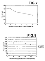
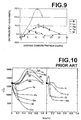
- Figure 10 is a graph illustrating Fig. 14 of the literature described above. Specifically, Figure 10 is a graph showing a relationship between a donor ion doping concentration and a dielectric constant.
- ferroelectric substances in which the donor ions have been doped at the A site at doping concentrations higher than those in " Effects of Impurity Doping in Lead Zirconate-Titanate Ceramics", S. Takahashi, Ferroelectrics, Vol. 41, pp. 143-156, 1982 , have been disclosed in, for example, Japanese Unexamined Patent Publication Nos. 2006-096647 , 2001-206769 , 2001-253774 , and 2006-188414 .
- a PZT type ferroelectric film in which Bi has been doped at the A site at a doping concentration falling within the range of more than 0 mol% to less than 100 mol%, and in which Nb or Ta has been doped at the B site at a doping concentration falling within the range of 5 mol% to 40 mol%, is disclosed in Japanese Unexamined Patent Publication No. 2006-096647 (Claim 1 thereof).
- the disclosed ferroelectric film is formed with a sol-gel technique.
- the sol-gel technique is the thermal-equilibrium processing.
- V used in Japanese Unexamined Patent Publication No. 2001-253774 acts as the donor ions at the B site.
- An ionic radius of V is smaller than the ionic radius of each of Nb and Ta, and it is considered that the effect of V as the donor ions will be smaller than the effect of each of Nb and Ta. Further, it is preferable that V 2 O 5 , which has a high toxicity, is not used.
- the donor ions having a high valence number and the acceptor ions having a low valence number are co-doped.
- the acceptor ions having a low valence number act to lower the ferroelectric characteristics.
- the effect of the donor ion doping is not always capable of being derived sufficiently.
- the ferroelectric substances should preferably take on the form of a thin film.
- the bulk sintered body is taken as the object.
- Japanese Unexamined Patent Publication No. 2006-096647 the formation of the ferroelectric filmwith the sol-gel technique is described.
- the sol-gel technique in cases where the film thickness is set to be large, cracks arise readily. Therefore, with the sol-gel technique, it is not always possible to form a thin film having a thickness larger than 1 ⁇ m.
- the ferroelectric film may be a thin film having a thickness of at most 1 ⁇ m.
- the film thickness of the ferroelectric film should preferably be at least 3 ⁇ m. It will be possible to set the film thickness to be large with a technique, wherein the lamination of a thin film is iterated. However, the technique for iterating the lamination of a thin film will not be practicable. Also, with the sol-gel technique, Pb deficiency is apt to occur. In cases where the Pb deficiency occurs, there is a tendency for the ferroelectric performance to become bad.
- a crystalline perovskite type film is formed at a deposition temperature of 500 °C.
- the composition of the film is 7 % La, 65 % Zr and 35 % Ti with Pb and O added stoichiometrically, assuming that the target composition matches the film composition. Any details regarding the sputtering procedure are not disclosed.
- US 6,287,986 B1 discloses a sputtering process for forming PLZT thin films on a substrate.
- Three shields are stacked vertically with a certain height at the periphery of the substrate.
- An alternating bias voltage is applied to the shield, and thus change over time of the ion energy is prevented, and the relative volume of the ion energy is controlled.
- the primary object of the present invention is to provide a process for forming a ferroelectric film containing a perovskite type oxide, which is of a PZT type, wherein a sintering auxiliary or acceptor ions need not be doped, and wherein donor ions are capable of being doped in a doping concentration of at least 5 mol% at an A site.
- the process shall yield a ferroelectric film containing a perovskite type oxide, which is of a PZT type, which has been doped with donor ions in a doping concentration of at least 5 mol% at an A site, and which has good ferroelectric performance.
- the process of the present invention shall also yield a ferroelectric film containing a perovskite type oxide, which is of a PZT type, which is free from A site deficiency, which has been doped with donor ions in a doping concentration of at least 5 mol% at the A site, and which has good ferroelectric performance.
- the process of the present invention shall yield a ferroelectric film containing a perovskite type oxide, which is of a PZT type, which has been doped with donor ions in a doping concentration of at least 5 mol% at an A site, and which has good ferroelectric performance, the ferroelectric film being capable of having a film thickness of at least 3.0 ⁇ m.
- ferroelectric device which comprises the ferroelectric film, and a liquid discharge apparatus utilizing the ferroelectric device.
- the present invention provides a process for forming a ferroelectric film on a substrate by a sputtering technique, the ferroelectric film containing a perovskite type oxide that is represented by Formula (P) shown below, wherein a target, which has a composition in accordance with the film composition of the ferroelectric film to be formed, and the substrate are located at a spacing from each other, a shield, which surrounds an outer periphery of the target on the substrate side, is located in a non-contact state with respect to the target, the shield being provided with a plurality of shielding layers, which are superposed one upon another at intervals with respect to the direction of the superposition, and the ferroelectric film is formed on the substrate by the sputtering technique under conditions of a height of the shield such that a difference Vs-Vf (V) between a plasma potential Vs (V) in plasma at the time of the film formation by the sputtering technique and a floating potential Vf (V) becomes equal to at most 35eV
- V s -V f (v) The difference V s -V f (v) is controlled by adjustments of the height of the shield.
- film formation temperature Ts (°C) as used herein means the center temperature of the substrate, on which the film is to be formed.
- each of the term "plasma potential Vs" and the term “floating potential Vf” as used herein means the value as measured with a single probe technique utilizing a Langmuir probe. Such that an error may not occur due to clinging of the film, which is being formed, or the like, to the probe, the measurement of the floating potential Vf should be performed as quickly as possible with a probe end being located in the vicinity of the substrate (at a position approximately 10mm spaced from the substrate).
- the potential difference Vs-Vf (V) between the plasma potential Vs and the floating potential Vf is capable of being converted directly into an electron temperature (eV).
- the electron temperature of 1eV corresponds to 11,600K (where K represents the absolute temperature).
- the process for forming a ferroelectric film in accordance with the present invention should preferably be modified such that M in Formula (P) represents Bi.
- the process for forming a ferroelectric film in accordance with the present invention should more preferably be modified such that x represents a number satisfying the condition of 0.05 ⁇ x ⁇ 0.25.
- the process for forming a ferroelectric film in accordance with the present invention is capable of providing the ferroelectric film containing the perovskite type oxide having a composition, in which ⁇ represents a number satisfying the condition of 0 ⁇ ⁇ ⁇ 0.2, and which is rich in A site element.
- the process for forming a ferroelectric film in accordance with the present invention is capable of providing the ferroelectric film containing the perovskite type oxide, which is substantially free from Si, Ge, and V.
- substantially free from Si, Ge, and V means that the concentration of each element, which concentration is detected with an X-ray fluorescence analysis from a surface of the perovskite type oxide (e.g., in the cases of a perovskite type oxide film, a surface of the film), is less than 0.1 wt% in the cases of Si and is less than 0.01% in the cases of each of Ge and V.
- the process of the present invention provides a ferroelectric film.
- the ferroelectric film obtainable by the process of the present invention is capable of being furnished as the ferroelectric film having characteristics such that a value of (Ec1+Ec2) / (Ec1-Ec2) ⁇ 100 (%) is equal to at most 25%, wherein Ec1 represents the coercive field on the positive electric field side in a bipolar polarization-electric field curve, and Ec2 represents the coercive field on the negative electric field side in the bipolar polarization-electric field curve.
- the ferroelectric film obtainable by the process of the present invention is capable of being furnished as the ferroelectric film having a film structure containing a plurality of pillar-shaped crystals.
- ferroelectric film obtainable by the process of the present invention is capable of being furnished as the ferroelectric film having a film thickness of at least 3.0 ⁇ m.
- ferroelectric device comprising:
- the inventors have found that, in cases where the film formation is performed by the sputtering technique, which is the non-thermal-equilibrium processing, the sintering auxiliary or the acceptor ions need not be doped, and the donor ions are capable of being doped in the doping concentration of at least 5 mol% at the A site of lead zirconate titanate (PZT). Specifically, the inventors have found that the donor ions are capable of being doped in the doping concentration falling within the range of 5 mol% to 40 mol% at the A site of PZT.
- M represents at least one kind of element selected from the group consisting of Bi and
- the ferroelectric film obtainable by the process of the present invention is characterized by containing the aforesaid perovskite type oxide.
- the present invention is capable of providing the ferroelectric film, which contains the aforesaid perovskite type oxide as a principal constituent.
- the term "principal constituent" as used herein means that the proportion of the constituent is equal to at least 80% by mass.
- ferroelectric substances described in Japanese Unexamined Patent Publication Nos. 2006-096647 , 2001-206769 , and 2001-253774 it is essential to dope Si, Ge, or V as the sintering auxiliary.
- the ferroelectric film containing the perovskite type oxide which is substantially free from Si, Ge, and V.
- Sn As the sintering auxiliary, there has also been known Sn.
- the doping of the sintering auxiliary or the acceptor ions causes the ferroelectric performance to become low.
- the ferroelectric film containing the perovskite type oxide formed in accordance with the process of the present invention wherein the sintering auxiliary or the acceptor ions need not be doped, the lowering of the ferroelectric performance due to the sintering auxiliary or the acceptor ions is capable of being suppressed, and the enhancement of the ferroelectric performance by the doping with the donor ions is capable of being derived sufficiently.
- the sintering auxiliary or the acceptor ions need not be doped.
- the sintering auxiliary or the acceptor ions may be doped within a range such that the adverse effect on the characteristics may not occur markedly.
- the perovskite type oxide contained in the ferroelectric film formed in accordance with the process of the present invention which perovskite type oxide has been doped with the donor ions in the doping concentration falling within the range of 5 mol% to 40 mol% at the A site, is advantageous over genuine PZT or PZT, which has been doped with the donor ions at the B site of PZT, in that the Pb concentration may be kept low, and in that a load on the environment may be kept light.
- the PZT film in which Nb, Ta, or W acting as the donor ions has been doped at the B site of PZT, exhibits an asymmetric hysteresis, in which a bipolar polarization-electric field curve (PE curve) is biased toward the positive electric field side, and that the ferroelectric film containing the perovskite type oxide formed in accordance with the process of the present invention, in which to donor ions have been doped at the A site, the asymmetric hysteresis of the PE curve is relieved to hysteresis close to a symmetric hysteresis.
- PE curve bipolar polarization-electric field curve
- the asymmetry of the PE hysteresis may be defined by the state in which the coercive field Ec1 on the positive electric field side and the absolute value of the coercive field Ec2 on the negative electric field side are different from each other (i.e., Ec1 ⁇
- the ferroelectric film is used in the form of a ferroelectric device, in which a bottom electrode, the ferroelectric film, and a top electrode are overlaid one upon another in this order. Either one of the bottom electrode and the top electrode is taken as a ground electrode, at which the applied electrode is fixed at 0V, and the other electrode is taken as an address electrode, at which the applied voltage is varied. Ordinarily, for easiness of actuation, the bottom electrode is taken as the ground electrode, and the top electrode is taken as the address electrode.
- state in which a negative electric field is applied to a ferroelectric film means that a negative voltage is applied to the address electrode.
- the term “state in which a positive electric field is applied to a ferroelectric film” as used herein means that a positive voltage is applied to the address electrode.
- the polarization is not apt to occur with the application of the positive electric field and is apt to occur with the application of the negative electric field.
- the piezoelectric characteristics are not apt to occur with the application of the positive electric field and are apt to occur with the application of the negative electric field.
- an actuation driver IC for the top electrode it is necessary for an actuation driver IC for the top electrode to be set for the negative voltage.
- the IC for the negative voltage is not used widely and requires a high IC development cost.
- an actuation driver IC for the positive electrode which IC has been used widely, is capable of being utilized.
- the production process is not capable of being kept simple.
- the ferroelectric film in accordance with the process of the present invention With the ferroelectric film formed in accordance with the process of the present invention, the PE curve becomes close to the symmetric hysteresis. Therefore, the ferroelectric film in accordance with the present invention is advantageous from the view point of easiness of the actuation.
- the level of the asymmetric hysteresis of the PE curve is capable of being evaluated with the value of (Ec1+Ec2) / (Ec1-Ec2) ⁇ 100 (%), wherein Ec1 represents the coercive field on the positive electric field side in the PE curve, and Ec2 represents the coercive field on the negative electric field side in the PE curve.
- a large value of (Ec1+Ec2)/(Ec1-Ec2) ⁇ 100 (%) represents that the asymmetry of the PE hysteresis is high.
- the process of the present invention is capable of providing the ferroelectric film having the characteristics such that the value of (Ec1+Ec2)/(Ec1-Ec2) ⁇ 100 (%) is equal to at most 25%.
- the perovskite type oxide contained in the ferroelectric film formed in accordance with the process of the present invention should preferably be modified such that M in Formula (P) represents Bi.
- M in Formula (P) represents Bi
- the inventors have found that, in cases where M in Formula (P) represents Bi, it is possible to obtain the ferroelectric film, which exhibits the PE curve close to the symmetric hysteresis, and which at the same time has good ferroelectric performance.
- M in Formula (P) represents Bi
- the perovskite type oxide contained in the ferroelectric film formed in accordance with the process of the present invention may contain a heterogeneous phase within a range such that the adverse effect on the characteristics may not occur markedly.
- XRD X-ray diffraction
- the inventors have found that, in cases where M in Formula (P) represents Bi, and x in Formula (P) represents a number falling within the range of 0.05 ⁇ x ⁇ 0.25, the perovskite type oxide is capable of being obtained, which exhibits a particularly high dielectric constant ⁇ , a particularly high maximum polarization intensity Pmax, and the like, and which has good ferroelectric performance. (Reference may be made to Example 1, which will be described later, and Figure 8 .) Therefore, from the view point of the ferroelectric performance, in cases where M in Formula (P) represents Bi, x in Formula (P) should preferably represent a number falling within the range of 0.05 ⁇ x ⁇ 0.25.
- x in Formula (P) should preferably represent a number falling within the range of 0.25 ⁇ x ⁇ 0.40, such that the Bi doping concentration may be higher than the range described above.
- y in Formula (P) which value is associated with the composition of Ti and Zr, should fall within the range of 0 ⁇ y ⁇ 0.7.
- the value of y in Formula (P) should preferably be set such that a composition in the vicinity of the composition at a morphotropic phase boundary (MPB), which represents the phase transition point between a tetragonal phase and a rhombohedral phase, may be obtained.
- MPB morphotropic phase boundary
- the value of y in Formula (P) should preferably fall within the range of 0.45 ⁇ y ⁇ 0.7, and should more preferably fall within the range of 0.47 ⁇ y ⁇ 0.57.
- the Pb deficiency is apt to occur.
- the ferroelectric performance it is possible to provide the ferroelectric film containing the perovskite type oxide having the composition, in which the value of ⁇ in Formula (P) falls within the range of ⁇ ⁇ 0, and which is free from deficiency in A site element.
- the ferroelectric film containing the perovskite type oxide having the composition in which the value of ⁇ in Formula (P) falls within the range of ⁇ > 0, and which is rich in A site element.
- the inventors have found that, in accordance with the process of the present invention, it is possible to provide the ferroelectric film containing the perovskite type oxide having the composition, in which the value of ⁇ in Formula (P) falls within the range of 0 ⁇ ⁇ ⁇ 0.2, and which is rich in A site element.
- the ferroelectric film containing the perovskite type oxide having the composition in which the value of ⁇ in Formula (P) falls within the range of ⁇ ⁇ 0, and which is free from the deficiency in A site element.
- the ferroelectric film containing the perovskite type oxide formed in accordance with the process of the present invention there may be present the A site deficiency within a range such that the adverse effect on the characteristics may not occur markedly.
- the film structure containing the plurality of the pillar-shaped crystals is not capable of being obtained.
- the film structure containing the plurality of the pillar-shaped crystals, each of which extends in a direction nonparallel with respect to a substrate surface it is possible to obtain an orientational film, in which the crystal orientation is uniform.
- the film structure containing the plurality of the pillar-shaped crystals, each of which extends in a direction nonparallel with respect to a substrate surface it is possible to obtain high piezoelectric performance. Examples of piezoelectric strains include the following:
- the ferroelectric film should preferably have the crystal orientational characteristics. For example, in the cases of the PZT type ferroelectric film, which has the MPB composition, a pillar-shaped crystal film having the (100) orientation is capable of being obtained.
- the direction of growth of the pillar-shaped crystals may be nonparallel with respect to the substrate surface.
- the direction of growth of the pillar-shaped crystals may be approximately normal to the substrate surface.
- the direction of growth of the pillar-shaped crystals may be oblique with respect to the substrate surface.
- the mean pillar diameter of the plurality of the pillar-shaped crystals, which constitute the ferroelectric film, is not limited and should preferably fall within the range of 30nm to 1 ⁇ m. If the mean pillar diameter of the pillar-shaped crystals is markedly small, there will be the risk that the crystal growth sufficient for the ferroelectric substance will not arise, and that the desired ferroelectric performance (piezoelectric performance) will not be capable of being obtained. If the mean pillar diameter of the pillar-shaped crystals is markedly large, there will be the risk that the shape accuracy after patterning processing has been performed will become low.
- the ferroelectric film which contains the perovskite type oxide represented by Formula (P), and which has a film thickness of at least 3.0 ⁇ m.
- the process of the present invention provides the ferroelectric film containing the perovskite type oxide, which is of the PZT type, and which has been doped with the donor ions in a doping concentration falling within the range of 5 mol% to 40 mol% at the A site, the ferroelectric film containing the perovskite type oxide being capable of being formed with the process wherein the sintering auxiliary or the acceptor ions need not be doped.
- the ferroelectric film containing the perovskite type oxide formed in accordance with the process of the present invention, which has been doped with the donor ions in the high doping concentration falling within the range of 5 mol% to 40 mol% at the A site has good ferroelectric performance (good piezoelectric performance).
- the ferroelectric film containing the perovskite type oxide formed in accordance with the process of the present invention wherein the sintering auxiliary or the acceptor ions need not be doped, and wherein the donor ions are capable of being doped in the high doping concentration described above at the A site, the lowering of the ferroelectric performance due to the sintering auxiliary or the acceptor ions is capable of being suppressed, and the enhancement of the ferroelectric performance by the doping with the donor ions is capable of being derived sufficiently.
- the ferroelectric film described above containing the perovskite type oxide that is represented by Formula (P), which perovskite type oxide has been doped with the donor ions M in the doping concentration falling within the range of 5 mol% to 40 mol% at the A site, is capable of being formed by the sputtering technique, which is the non-thermal-equilibrium processing.
- the film formation techniques appropriate for the ferroelectric film described above include the sputtering technique, a plasma enhanced chemical vapor deposition technique (a plasma enhanced CVD technique), a firing quenching technique, an annealing quenching technique, and a flame spraying quenching technique.
- the sputtering technique is particularly preferable.
- the thermal-equilibrium processing such as the sol-gel technique
- the contrivance as described above is not necessary, and the donor ions are capable of being doped in a high doping concentration.
- the sputtering apparatus should preferably be constituted such that the sputtering apparatus is provided with the shield, which surrounds the outer periphery of a target holder on the film formation substrate side, and such that the state of the potential of the plasma space is capable of being adjusted by the presence of the shield.
- the shield which surrounds the outer periphery of a target holder on the film formation substrate side
- the state of the potential of the plasma space is capable of being adjusted by the presence of the shield.
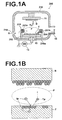
- FIG. 1A is a schematic sectional view showing a film forming apparatus (a sputtering apparatus) employed in this embodiment.
- Figure 1B is an explanatory view showing how a film is formed.
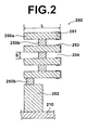
- Figure 2 is an enlarged view showing a shield and its vicinity in Figure 1A .
- a film forming apparatus 200 is approximately constituted of a vacuum chamber 210, in which a substrate holder 11, such as an electrostatic chuck, and a plasma electrode (a cathode electrode) 12 are provided.
- the substrate holder 11 is capable of supporting a substrate (a film formation substrate) B and heating the substrate B to a predetermined temperature.
- the plasma electrode 12 acts to generate plasma.
- the plasma electrode 12 corresponds to the target holder for supporting a target T.
- the substrate holder 11 and the plasma electrode 12 are located at a spacing from each other so as to stand facing each other. Also, a target T, which has a composition in accordance with the composition of the film to be formed, is located on the plasma electrode 12.
- the plasma electrode 12 is connected to a radiofrequency electric power source 13.
- the plasma electrode 12 and the radiofrequency electric power source 13 together constitute a plasma forming section.
- the film forming apparatus 200 is provided with a shield 150, which surrounds the outer periphery of the target T on the film formation substrate side.
- This constitution may be expressed such that the film forming apparatus 200 is provided with the shield 250, which surrounds the outer periphery of the plasma electrode 12 for supporting the target T, i.e., the outer periphery of the target holder, on the film formation substrate side.
- the vacuum chamber 210 is provided with a gas introducing aperture 214, through which a gas (film formation gas) G necessary for the film formation is to be introduced into the vacuum chamber 210.
- the vacuum chamber 210 is also provided with a gas exhaust pipe 15, through which an exhaust gas V is to be taken out from the vacuum chamber 210.
- the gas introducing aperture 214, through which the gas G is to be introduced into the vacuum chamber 210, is located on the side opposite to the gas exhaust pipe 15 and at the height approximately identical with the height of the shield 250.
- an Ar gas, an Ar/O 2 mixed gas, or the like is utilized as the gas G.
- the gas G having been introduced into the vacuum chamber 210 is converted into the plasma by electrical discharge of the plasma electrode 12, and a plus ion Ip, such as an Ar ion, is thereby produced.
- the plus ion Ip having thus been produced sputters the target T.
- a constituent element Tp of the target T having thus been sputtered by the plus ion Ip is released from the target T and is deposited on the substrate B in a neutral state or in an ionized state.
- a reference letter P represents a plasma space.
- the potential of the plasma space P constitutes the plasma potential Vs (V).
- the substrate B is an electrical insulator and is electrically isolated from the ground. Therefore, the substrate B is in a floating state, and the potential of the substrate B constitutes the floating potential Vf (V). It is considered that the constituent element Tp of the target T, which constituent element is located between the target T and the substrate B, collides with the substrate B during the film formation by having kinetic energy corresponding to acceleration voltage of the potential difference Vs-Vf between the potential of the plasma space P and the potential of the substrate B.
- the plasma potential Vs and the floating potential Vf are capable of being measured by use of the Langmuir probe.
- the probe potential, at which the current becomes equal to zero is the floating potential Vf. In this state, the quantities of the ion current and the electron current flowing into the probe surface become equal to each other.
- a metal surface and the substrate surface in the electrically isolated state are set at the floating potential Vf.
- the ion current decreases successively, and only the electron current reaches the probe.
- the voltage at the boundary is the plasma potential Vs.
- the difference Vs-Vf has the correlation with the kinetic energy of the constituent element Tp of the target T, which constituent element collides with the substrate B.
- the kinetic energy E may be represented by a function of the temperature T. Therefore, it is considered that the difference Vs-Vf has the effects identical with the effects of the temperature upon the substrate B.
- Vs-Vf also has the effects of promoting the surface migration, the effects of etching the weak binding regions, and the like.
- the vacuum chamber 210 illustrated in Figure 1A is characterized by the provision of the shield 250, which is located within the vacuum chamber 210 so as to surround the outer periphery of the target T on the film formation substrate side.
- the shield 250 is located on a ground shield, i.e., a grounding member 202, so as to surround the outer periphery of the target T on the film formation substrate side.
- the grounding member 202 stands on a bottom surface 210a of the vacuum chamber 210 so as to surround the plasma electrode 12.
- the grounding member 202 acts to prevent electrical discharge from the plasma electrode 12 laterally or downwardly toward the vacuum chamber 210.
- the shield 250 is provided with a plurality of annular metal plates, i.e., rings (or fins or shielding layers) 250a, 250a, ....
- the shield 250 is provided with four sheets of the rings 250a, 250a, ..., and a plurality of electrically conductive spacers 250b, 250b, ... are located between the adjacent rings 250a, 250a.
- the plurality of the spacers 250b, 250b, ... are located at intervals along the circumferential direction of each of the rings 250a, 250a, ...
- a plurality of the spacers 250b, 250b, ... should preferably be located also between the grounding member 202 and the ring 250a that is located just above the grounding member 202.
- the shield 250 is electrically connected with the grounding member 202 and is thus grounded.
- No limitation is imposed upon the materials of the rings 250a, 250a, ..., and the spacers 250b, 250b, ....
- the rings 250a, 250a, ..., and the spacers 250b, 250b, ... should preferably be made from stainless steel (SUS), or the like.
- the constitution described above may be modified such that electrical connection members (not shown) for electrically connecting the plurality of the rings 250a, 250a, ... with one another are fitted to the outer periphery side of the shield 250.
- the rings 250a, 250a, ... of the shield 250 are electrically connected with one another by the electrically conductive spacers 250b, 250b, ... and are thus capable of being grounded.
- the electrical connection members (not shown) described above are fitted to the outer periphery side of the shield 250, the plurality of the rings 250a, 250a, ... of the shield 250 are capable of being grounded reliably.
- the shield 250 is located so as to surround the outer periphery of the target T on the film formation substrate side. Therefore, a grounding potential is formed by the shield 250 at the outer periphery of the target T on the film formation substrate side.
- the plasma conditions are capable of being adjusted and optimized by the shield 250 having the constitution described above, and the difference Vs-Vf (V), which is the difference between the plasma potential Vs (V) and the floating potential Vf (V), is capable of being adjusted and optimized by the shield 250.
- Vs-Vf (V) which is the difference between the plasma potential Vs (V) and the floating potential Vf (V)
- the aforesaid effects of the shield 250 are considered as described below.
- the plasma is formed above the target T, and electrical discharge occurs between the shield 250 and the target T. It is considered that, due to the thus occurring electrical discharge, the plasma is confined within the region defined by the shield 250, the plasma potential Vs (V) is caused to become low, and the difference Vs-Vf (V), which is the difference between the plasma potential Vs (V) and the floating potential Vf (V), is thus caused to become low.
- the value of the difference Vs-Vf (V) most appropriate as the film formation conditions is capable of being obtained.
- V the value of the difference Vs-Vf (V) most appropriate as the film formation conditions.
- the ring 250a which is located at the bottom end of the shield 250, is located at a spacing from the outer periphery of the target T. If the linear distance of the spacing between the target T and the shield 250 is zero, the electrical discharge will not occur. Also, if the linear distance of the spacing between the target T and the shield 250 is markedly long, the effects of the shield 250 will become small. Therefore, in order for the effects of the shield 250 to be obtained efficiently, the spacing distance between the target T and the shield 250 should preferably fall within the range of approximately 1mm to approximately 30mm.
- the constituent element Tp of the target T having been released from the target T is deposited on the substrate B and is also deposited on the rings 250a, 250a, ... of the shield 250 located around the target T.
- the constituent element Tp of the target T is deposited predominantly on an inner peripheral edge 251 of each of the rings 250a, 250a, ..., which inner peripheral edge 251 stands facing the target T, and on the regions in the vicinity of the inner peripheral edge 251.
- the state of the deposition is illustrated in Figure 2 .
- particles (deposition particles) of the constituent element Tp are deposited to form a film 253 on the inner peripheral edge 251 of each of the rings 250a, 250a, ...
- the shield 250 should preferably be constituted such that the film 253 may not be formed as much as possible.
- the shield 250 is provided with the plurality of the rings 250a, 250a, ..., which are superposed one upon another at intervals with respect to the direction of the superposition, such that the space 204 may intervene between the adjacent rings 250a, 250a. Therefore, the problems are capable of being prevented from occurring in that the deposition particles of the constituent element Tp having been released from the target T are deposited on the entire area of the shield 250, and in that the state of the potential of the shield 250 is thus caused to alter. Accordingly, in cases where the film formation is iterated, the shield 250 is capable of functioning reliably, and the difference Vs-Vf (V) between the plasma potential Vs (V) and the floating potential Vf (V) is capable of being kept reliably.
- a thickness L of the wall material of the shield 250 which thickness is taken in the direction normal to the direction of the superposition of the rings 250a, 250a, ... acting as the shielding layers, and a distance S between the rings 250a, 250a, which are adjacent to each other with respect to the direction of the superposition, i.e. the distance S between the adjacent shielding layers, should preferably have the relationship expressed as L ⁇ S.
- the relationship described above has the effects such that the thickness L of the wall material of the shield 250 may be set to be large within a predetermined range with respect to the distance S between the adjacent rings 250a, 250a, and such that the film 253 may not be apt to be deposited over the entire area of each of the rings 250a, 250a, ....
- the constituent element Tp is not capable of easily entering toward the outer periphery side of the space 204, and the problems are capable of being prevented from occurring in that the shield 250 quickly loses its functions.
- the space 204 also has other effects. Specifically, since the space 204 fulfils the roles as the path for the film formation gas G, the film formation gas G is capable of passing through the space 204 of the shield 250 and is thus capable of easily arriving at the plasma space in the vicinity of the target T. Therefore, the gas ion having been converted into the plasma in the vicinity of the target T is capable of easily arriving at the target T and is capable of efficiently causing the constituent element Tp of the target T to be released from the target T. As a result, the film having good quality and the desired characteristics is capable of being formed reliably.
- the shield 250 having the space 204 forms a wall of the equal potential on the inner periphery side. Therefore, the shield 250 having the space 204 has the effects of adjusting the difference Vs-Vf (V), which effects are of the level equivalent to the level of the effects of the shield free from the space.
- the difference Vs-Vf (V) is capable of being controlled by the adjustment of the height of the shield 250.
- the difference Vs-Vf (V) is also capable of being adjusted by an alteration of the electric power applied to the target T, the film formation pressure, or the like.
- the problems often occur in that a different parameter, such as the film formation rate, alters, and therefore the desired film quality is not capable of being obtained.
- the inventors have found that the film formation should be performed under the film formation conditions such that the difference Vs-Vf (V) between the plasma potential Vs (V) and the floating potential Vf (V) is equal to at most 35eV, and such that the temperature of the substrate B is equal to at least 400°C.
- the perovskite crystal containing little pyrochlore phase is capable of being caused to grow reliably
- the occurrence of the Pb deficiency is capable of being suppressed reliably
- the ferroelectric film having good quality which has a good crystal structure and a good film composition, is capable of being formed reliably.
- the characteristics such that the element is apt to be sputtered represent that the atom is apt to be re-sputtered after the atom has been deposited on the substrate surface. It is considered that, as the difference between the plasma potential and the potential of the substrate becomes large, i.e. as the difference Vs-Vf becomes large, the re-sputtering rate becomes high, and the Pb deficiency becomes apt to occur.
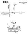
- FIG. 4 is a sectional view showing a major part of an ink jet type recording head (acting as a liquid discharge apparatus), which is provided with an embodiment of the piezoelectric device described above.
- Figure 4 for clearness, reduced scales of constituent elements of the ink jet type recording head are varied from actual reduced scales.
- a piezoelectric device (a ferroelectric device) 2 comprises a substrate 20.
- the piezoelectric device 2 also comprises a bottom electrode 30, a ferroelectric film (a piezoelectric film) 40, and top electrodes 50, 50, ..., which are overlaid in this order on a surface of the substrate 20.
- An electric field is capable of being applied by the bottom electrode 30 and each of the top electrodes 50, 50, ... in the thickness direction of the ferroelectric film 40.
- the ferroelectric film 40 is constituted of the ferroelectric film obtainable by the process in accordance with the present invention, which contains the perovskite type oxide represented by Formula (P) shown above.
- the bottom electrode 30 is formed over approximately the entire area of the surface of the substrate 20.
- the ferroelectric film 40 is formed on the bottom plate 30.
- the ferroelectric film 40 has a pattern comprising line-like protruding areas 41, 41, ..., which extend along a line normal to the plane of the sheet of Figure 3 and are arrayed in a striped pattern.
- Each of the top electrodes 50, 50, ... is formed on one of the protruding areas 41, 41, ....
- the pattern of the ferroelectric film 40 is not limited to the one illustrated in Figure 4 and may be designed arbitrarily.
- the ferroelectric film 40 may be formed as a continuous film.
- the ferroelectric film 40 is not formed as a continuous film and is formed in the pattern comprising the plurality of the protruding areas 41, 41, ... separated from one another, the expansion and the contraction of each of the protruding areas 41, 41, ... are capable of occurring smoothly, and therefore a large displacement quantity is capable of being obtained.
- the ferroelectric film 40 should preferably be formed in the pattern comprising the plurality of the protruding areas 41, 41, ... separated from one another.
- the substrate 20 may also be constituted of a laminate substrate, such as an SOI substrate, which contains an SiO 2 oxide film having been formed on a surface of a silicon substrate.
- the principal constituents of the bottom electrode 30 include metals, such as Au, Pt, and Ir; metal oxides, such as IrO 2 , RuO 2 , LaNiO 3 , and SrRUO 3 ; and combinations of the above-enumerated metals and/or the above-enumerated metal oxides.
- top electrodes 50, 50, ... examples include the materials exemplified above for the bottom electrode 30; electrode materials ordinarily utilized in semiconductor processes, such as Al, Ta, Cr, and Cu; and combinations of the materials exemplified above for the bottom electrode 30 and/or the above-enumerated electrode materials.
- the thickness of the bottom electrode 30 and the thickness of each of the top electrodes 50, 50, .... may be approximately 200nm.
- the thickness of the ferroelectric film 40 may ordinarily be at least 1 ⁇ m and may fall within the range of, for example, 1 ⁇ m to 5 ⁇ m.
- the thickness of the ferroelectric film 40 should preferably be at least 3 ⁇ m.
- An ink jet type recording head (acting as the liquid discharge apparatus described above) 3 approximately has a constitution, in which a vibrating plate 60 is secured to a bottom surface of the substrate 20 of the piezoelectric device 2 having the constitution described above, and in which an ink nozzle (acting as the liquid storing and discharging member) 70 is secured to the bottom surface of the vibrating plate 60.
- the ink nozzle 70 comprises a plurality of ink chambers (acting as the liquid storing chambers) 71, 71, ..., in which ink is to be stored.
- the ink nozzle 70 also comprises a plurality of ink discharge openings (acting as the liquid discharge openings) 72, 72, ..., through which the ink is to be discharged from the ink chambers 71, 71, ... to the exterior of the ink chambers 71, 71, ....
- the plurality of the ink chambers 71, 71, ... are located in accordance with the number and the pattern of the protruding areas 41, 41, ... of the ferroelectric film 40.
- the ink jet type recording head 3 is constituted such that each of the protruding areas 41, 41, ... of the piezoelectric device 2 is expanded or contracted through alteration of the electric field applied across each of the protruding areas 41, 41, ... of the piezoelectric device 2, and such that the discharge of the ink from each of the ink chambers 71, 71, ... and the quantity of the ink discharged from each of the ink chambers 71, 71, ... are thereby controlled.
- a part of the substrate 20 may be processed to form the vibrating plate 60 and the ink nozzle 70.
- the substrate 20 is constituted of the laminate substrate, such as the SOI substrate
- etching processing may be performed on the substrate 20 from the rear surface side of the substrate 20 in order to form the ink chamber 71, and the vibrating plate 60 and the ink nozzle 70 may be formed with processing of the substrate 20.
- the embodiment of the piezoelectric device 2 and the ink jet type recording head 3 are constituted in the manner described above.
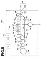
- Figure 5 is a schematic view showing an example of an ink jet type recording system, in which the aforesaid embodiment of the ink jet type recording head of Figure 4 is employed.
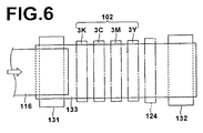
- Figure 6 is a plan view showing a part of the ink jet type recording system of Figure 5 .
- an ink jet type recording system 100 comprises a printing section 102, which is provided with a plurality of ink jet type recording heads (hereinbelow referred to simply as the heads) 3K, 3C, 3M, and 3Y. Each of the heads 3K, 3C, 3M, and 3Y is utilized for one of different ink colors.
- the ink jet type recording system 100 also comprises an ink stocking and loading section 114 for storing ink compositions, each of which is to be furnished to one of the heads 3K, 3C, 3M, and 3Y.
- the ink jet type recording system 100 further comprises a paper supply section 118 for supplying recording paper 116.
- the ink jet type recording system 100 still further comprises a de-curling processing section 120 for eliminating roll set curl of the recording paper 116 having been received from the paper supply section 118.
- the ink jet type recording system 100 also comprises a suction belt conveyor section 122, which is located so as to stand facing a nozzle bottom surface (i.e., an ink discharge surface) of the printing section 102.
- the suction belt conveyor section 122 conveys the recording paper 116, while flatness of the recording paper 116 is being kept.
- the ink jet type recording system 100 further comprises a print detecting section 124 for reading out the results of the printing performed with the printing section 102.
- the ink jet type recording system 100 still further comprises a paper discharge section 126 for discharging the printed recording paper (i.e., the printed paper) to the exterior of the ink jet type recording system 100.
- Each of the heads 3K, 3C, 3M, and 3Y of the printing section 102 is constituted of the aforesaid embodiment of the ink jet type recording head 3.
- the de-curling processing section 120 heat is given by a heating drum 130 to the recording paper 116 in the direction reverse to the direction of the roll set curl, and the de-curling processing is thereby performed.
- a cutter 128 is located at the stage after the de-curling processing section 120, and the rolled paper is cut by the cutter 128 into a desired size.
- the cutter 128 is constituted of a stationary blade 128A, which has a length equal to at least the width of the conveyance path for the recording paper 116, and a round blade 128B, which is capable of being moved along the stationary blade 128A.
- the stationary blade 128A is located on the side of the rear surface of the recording paper 116, which rear surface is opposite to the printing surface of the recording paper 116.
- the round blade 128B is located on the side of the printing surface of the recording paper 116 with the conveyance path intervening between the stationary blade 128A and the round blade 128B. In the cases of a system utilizing cut paper sheets, the system need not be provided with the cutter 128.
- the recording paper 116 which has been subjected to the de-curling processing and has then been cut into the desired size, is sent into the suction belt conveyor section 122.
- the suction belt conveyor section 122 has the structure, in which an endless belt 133 is threaded over two rollers 131 and 132.
- the suction belt conveyor section 122 is constituted such that at least a part of the suction belt conveyor section 122, which part stands facing the nozzle bottom surface of the printing section 102 and a sensor surface of the print detecting section 124, may constitute a horizontal surface (a flat surface).
- the belt 133 has a width larger than the width of the recording paper 116.
- the belt 133 has a plurality of suction holes (not shown), which are open at the belt surface.
- a suction chamber 134 is located within the space defined by the belt 133, which is threaded over the two rollers 131 and 132. Specifically, the suction chamber 134 is located at the position that stands facing the nozzle bottom surface of the printing section 102 and the sensor surface of the print detecting section 124. The region within the suction chamber 134 is evacuated into a negative pressure by use of a fan 135, and the recording paper 116 located on the belt 133 is thereby supported by suction on the belt 133.
- Rotation power of a motor (not shown) is transferred to at least either one of the rollers 131 and 132, over which the belt 133 is threaded.
- the belt 133 is thus rotated clockwise in Figure 5 , and the recording paper 116 having been supported on the belt 133 is thereby conveyed toward the right in Figure 5 .
- a belt cleaning section 136 is located at a predetermined position on the side outward from the space defined by the belt 133 (specifically, at an appropriate position other than the printing region).
- a heating fan 140 is located on the side upstream from the printing section 102 with respect to the paper conveyance path, which is formed by the suction belt conveyor section 122.
- the heating fan 140 blows dry air against the recording paper 116 before being subjected to the printing and thereby heats the recording paper 116. In cases where the recording paper 116 is thus heated just before the recording paper is subjected to the printing, the ink composition having been jetted out onto the recording paper 116 is capable of drying easily.
- the printing section 102 is constituted of the full-line type heads.
- the line type heads having a length corresponding to a maximum paper width are located so as to extend in the direction (i.e., the main scanning direction), which is normal to the paper feed direction.
- Each of the heads 3K, 3C, 3M, and 3Y is constituted of the line type head provided with a plurality of ink discharge openings (of the nozzles), which are arrayed over a length at least longer than one side of the recording paper 116 of the maximum size to be processed by the ink jet type recording system 100.
- the heads 3K, 3C, 3M, and 3Y corresponding to the ink colors are located in the order of black (K), cyan (C), magenta (M), and yellow (Y) from the upstream side with respect to the feed direction of the recording paper 116.
- the color ink compositions are discharged respectively from the heads 3K, 3C, 3M, and 3Y, while the recording paper 116 is being conveyed. A color image is thus recorded on the recording paper 116.
- the print detecting section 124 may be constituted of, for example, a line sensor for imaging the results of the droplet jetting-out operation performed by the printing section 102.
- the print detecting section 124 thus detects discharge failures, such as nozzle clogging, in accordance with the droplet jetting-out image having been read out by the line sensor.
- a post-drying section 142 is located at the stage after the print detecting section 124.
- the post-drying section 142 may be constituted of, for example, a heating fan for drying the printed image surface.
- the printing surface should preferably be free from contact with a drying member, or the like. Therefore, the post-drying section 142 should preferably employ a drying technique for blowing hot air against the printing surface.
- a heating and pressure applying section 144 is located at the stage after the post-drying section 142.
- a pressure is applied to the image surface by a press roller 145 having a predetermined surface recess-protrusion pattern, while the image surface is being heated. The recess-protrusion pattern is thus transferred from the press roller 145 to the image surface.
- the printed paper having thus been obtained is then discharged through the paper discharge section 126.
- the printed paper, on which a regular image (an object image) to be recorded has been printed, and the printed paper, on which a test printing image has been printed, should preferably be discharged to different destinations.
- the ink jet type recording system 100 is provided with sorting means (not shown) for sorting out the printed paper, on which the regular image to be recorded has been printed, and the printed paper, on which the test printing image has been printed, and changing over the paper discharge paths to each other in order to send the printed paper, on which the regular image to be recorded has been printed, and the printed paper, on which the test printing image has been printed, into a discharge section 126A and a discharge section 126B, respectively.
- a cutter 148 may be located in order to separate the paper sheet region, on which the test printing image has been printed, from the paper sheet region, on which the regular image to be recorded has been printed.
- the ink jet type recording system 100 is constituted in the manner described above.
- a commercially available sputtering apparatus was prepared. Five sheets of the rings 250a, 250a, ... made from stainless steel (SUS), each of which had an inner diameter of 130mm, an outer diameter of 180mm, and a thickness of 1mm, were set at the grounding potential and located along a side of a target T having a diameter of 120mm in the sputtering apparatus. In this manner, the film forming apparatus as illustrated in Figure 1A was obtained. The rings 250a, 250a, ... were superposed one upon another such that pillar-shaped, electrically conductive spacers 250b, 250b, ..., each of which had a diameter of 10mm and a thickness of 5mm, intervened between the adjacent rings 250a, 250a.
- SUS stainless steel
- Each of the spacers 250b, 250b, ... was sufficiently smaller than the size of each of the rings 250a, 250a, .... Therefore, the gas G having been introduced into the vacuum chamber 210 was capable of passing through the space 204 between the adjacent rings 250a, 250a without being adversely affected by the spacers 250b, 250b, ... and was thus capable of easily arriving at the target T.
- the spacing distance between the substrate B and the target T was set at 60mm.
- An electric power of 700W was applied to the radiofrequency electric power source under the conditions of a vacuum degree of 0.5Pa and in an Ar/O 2 mixed atmosphere (O 2 volume fraction: 2.5%).
- the number of the sheets of the rings 250a, 250a, ... was set at various different values falling within the range of 0 to four sheets, and the measurement was made in the same manner as that described above.
- Figure 7 shows the relationship between the number of sheets of the rings 250a, 250a, ... and the difference Vs-Vf (V).
- the difference Vs-Vf (V) became small in accordance with an increase of the number of the sheets of the rings 250a, 250a, ....
- the difference Vs-Vf (V) was thus capable of being controlled by the alteration of the number of the sheets of the rings 250a, 250a, ....
- an electrode-fitted substrate in which a 30nm-thick Ti close contact layer and a 300nm-thick Ir bottom electrode had been overlaid in this order on a 25mm-square Si substrate, was prepared.
- film formation was performed by use of the aforesaid RF sputtering apparatus, in which the number of the sheets of the rings 250a, 250a, ... was set at five sheets, under the same conditions as those described above.
- the target composition was set at various different compositions, and each of a plurality of kinds of Bi-doped PZT ferroelectric films having different Bi doping concentrations was thereby formed.
- the film formation temperature Ts was set at 450°C.
- the film thickness of the ferroelectric film was set at 5 ⁇ m.
- the Bi-doped PZT will hereinbelow be referred to as Bi-PZT.
- a Pt top electrode having a thickness of 100nm was formed on each of the aforesaid ferroelectric films by use of the sputtering technique. In this manner, each of ferroelectric devices in accordance with the present invention was obtained.
- La-doped PZT ferroelectric film having an identical La doping concentration was performed a plurality of times in the same manner as that described above, except that the target composition was altered. With respect to each of the La-doped PZT ferroelectric films having the identical La doping concentration, the ferroelectric device was obtained.
- the La-doped PZT will hereinbelow be referred to as La-PZT.
- Nb-doped PZT ferroelectric films having different Nb doping concentrations were formed in the same manner as that described above, except that the target composition was altered. With respect to each of the Nb-doped PZT ferroelectric films having thus been formed, the ferroelectric device was obtained.
- the Nb-doped PZT will hereinbelow be referred to as Nb-PZT.
- each of a plurality of kinds of Bi, Nb co-doped PZT ferroelectric films having different Bi doping concentrations and different Nb doping concentrations was performed in the same manner as that described above, except that the target composition was altered. With respect to each of the Bi, Nb co-doped PZT ferroelectric films having thus been formed, the ferroelectric device was obtained.
- the Bi, Nb co-doped PZT will hereinbelow be referred to as Bi, Nb-PZT.
- Ta-doped PZT ferroelectric films having different Ta doping concentrations were formed in the same manner as that described above, except that the target composition was altered. With respect to each of the Ta-doped PZT ferroelectric films having thus been formed, the ferroelectric device was obtained.
- the Ta-doped PZT will hereinbelow be referred to as Ta-PZT.
- each of a plurality of kinds of W-doped PZT ferroelectric films having different W doping concentrations was performed in the same manner as that described above, except that the target composition was altered. With respect to each of the W-doped PZT ferroelectric films having thus been formed, the ferroelectric device was obtained.
- the W-doped PZT will hereinbelow be referred to as W-PZT.
- each of the plurality of kinds of the Bi-PZT ferroelectric films having the different Bi doping concentrations had the composition, which might be represented by the formula shown below: (Pb 1-x+ ⁇ Bi x ) (Zr 0.52 Ti 0.48 ) O z
- the composition analysis with EDX was performed in the same manner as that described above.
- each of the plurality of kinds of the Bi-PZT ferroelectric films having the different Bi doping concentrations SEM cross-sectional observation was performed. It was found that each of the plurality of kinds of the Bi-PZT ferroelectric films having the different Bi doping concentrations was a pillar-shaped crystal structure film containing a plurality of pillar-shaped crystals (mean pillar diameter: approximately 150nm) having been grown in the direction approximately normal to the substrate surface.
- Each of the Bi-PZT films having the Bi doping concentration falling within the range of 6 mol% to 30 mol% was the film of the perovskite single phase structure having the (100) orientation.
- Figure 8 is a graph showing relationship between a Bi doping concentration (a molar concentration at the A site) and a maximum polarization intensity Pmax, which relationship has been obtained with respect to each of Bi-PZT films having been formed in Example 1.
- the sintering auxiliary or the acceptor ions need not be doped, and the donor ions were capable of being doped in the doping concentration of at least 5 mol% at the A site of PZT, and that high ferroelectric performance was capable of being obtained with the doping concentration falling within the range of 5 mol% to 20 mol%.
- the PE hysteresis measurement was performed with respect to the La-PZT films, the Nb-PZT films, Ta-PZT films, and W-PZT films. Also, with respect to the various kinds of the PZT type films having been formed in Example 1, calculations were made to find relationships among a kind of donor ions, a donor ion doping concentration, and a value of (Ec1+Ec2)/(Ec1-Ec2) ⁇ 100 (%). The results as illustrated in Figure 9 were obtained.
- the parameter value of (Ec1+Ec2) / (Ec1-Ec2) ⁇ 100 (%) representing the level of the asymmetry of the PE hysteresis was large and exceeded 25%.
- the parameter value described above was small, and good symmetry of the PE hysteresis was capable of being obtained.
- the parameter value fell within the range of (Ec1+Ec2)/(Ec1-Ec2) ⁇ 100 (%) ⁇ 25. Also, it was revealed that, as for the Bi, Nb-PZT film, in which the donor ions were doped at the A site and the B site, the asymmetry of the PE hysteresis was relieved than the PE hysteresis of the Nb-PZT film, in which the donor ions were doped only at the B site.
- the ferroelectric film formed in accordance with the process of the present invention is capable of being utilized appropriately for the ferroelectric devices for piezoelectric actuators for use in ink jet type recording heads, magnetic recording and reproducing heads, micro electro-mechanical systems (MEMS) devices, micro pumps, ultrasonic probes, and the like.
- MEMS micro electro-mechanical systems
- the ferroelectric film formed in accordance with the process of the present invention is also capable of being utilized appropriately for the ferroelectric devices for ferroelectric memories, and the like.
Description
- This invention relates to a process for forming a ferroelectric film containing a perovskite type oxide, which is of a PZT type. Described herein is also a ferroelectric film obtainable by the process for forming a ferroelectric film, a ferroelectric device, which comprises the ferroelectric film, and a liquid discharge apparatus utilizing the ferroelectric device.
- Piezoelectric devices provided with a piezoelectric body, which has piezoelectric characteristics such that the piezoelectric body expands and contracts in accordance with an increase and a decrease in electric field applied across the piezoelectric body, and electrodes for applying the electric field across the piezoelectric body have heretofore been used for use applications, such as actuators to be loaded on ink jet type recording heads. As piezoelectric body materials, there have heretofore been widely used perovskite type oxides, such as lead zirconate titanate (PZT). The materials described above are ferroelectric substances, which have spontaneous polarization characteristics at the time free from electric field application.
- It has been known from the 1960s that PZT having been doped with donor ions having a valence number higher than the valence number of substitutable ions exhibit the characteristics, such as ferroelectric performance, having been enhanced over the characteristics of genuine PZT. As the donor ions capable of substituting Pb2+ ions at an A site, there have been known Bi3+ ions and various kinds of lanthanoid cations, such as La3+ ions. As the donor ions capable of substituting Zr4+ ions and/or Ti4+ ions at a B site, there have been known V5+ ions, Nb5+ ions, Ta5+ ions, Sb5+ ions, Mo6+ ions, W6+ ions, and the like.
- The ferroelectric substances have heretofore been produced with, for example, a technique wherein multiple kinds of oxide particles containing constituent elements for a desired composition are mixed together, and wherein the thus obtained mixed particles are subjected to molding processing and firing processing, or a technique wherein multiple kinds of oxide particles containing constituent elements for a desired composition are dispersed in an organic binder, and wherein the thus obtained dispersion is coated on a substrate and fired. With the aforesaid techniques for producing the ferroelectric substances, the ferroelectric substances have been produced via the firing processing at a temperature of at least 600°C, ordinarily at a temperature of at least 1,000°C. With the aforesaid techniques for producing the ferroelectric substances, since the production processing is performed in the high-temperature thermal-equilibrium state, a dopant having a valence number, which does not match, is not capable of being doped at a high concentration.
- Studies on doping of various kinds of donor ions to a PZT bulk ceramic material are described in, for example, "Effects of Impurity Doping in Lead Zirconate-Titanate Ceramics", S. Takahashi, Ferroelectrics, Vol. 41, pp. 143-156, 1982.
Figure 10 is a graph illustrating Fig. 14 of the literature described above. Specifically,Figure 10 is a graph showing a relationship between a donor ion doping concentration and a dielectric constant. InFigure 10 , it is illustrated that the characteristics become best at a donor ion doping concentration of approximately 1.0 mol% (corresponding to approximately 0.5 wt% in the cases ofFigure 10 ), and that the characteristics become bad in cases where the donor ion doping concentration is higher than approximately 1.0 mol%. It is presumed that, in cases where the donor ion doping concentration is higher than approximately 1.0 mol%, a part of the donor ions, which part are not capable of forming a solid solution because of valence number mismatch, undergo segregation at particle boundaries, and the like, and the characteristics are thus caused to become bad. - Recently, ferroelectric substances, in which the donor ions have been doped at the A site at doping concentrations higher than those in "Effects of Impurity Doping in Lead Zirconate-Titanate Ceramics", S. Takahashi, Ferroelectrics, Vol. 41, pp. 143-156, 1982, have been disclosed in, for example, Japanese Unexamined Patent Publication Nos.
2006-096647 2001-206769 2001-253774 2006-188414 - A PZT type ferroelectric film, in which Bi has been doped at the A site at a doping concentration falling within the range of more than 0 mol% to less than 100 mol%, and in which Nb or Ta has been doped at the B site at a doping concentration falling within the range of 5 mol% to 40 mol%, is disclosed in Japanese Unexamined Patent Publication No.
2006-096647 Claim 1 thereof). The disclosed ferroelectric film is formed with a sol-gel technique. The sol-gel technique is the thermal-equilibrium processing. With the ferroelectric film disclosed in Japanese Unexamined Patent Publication No.2006-096647 2006-096647 2006-096647 2006-096647 2006-096647
[0114] of Japanese Unexamined Patent Publication No.2006-096647 2001-206769 2001-253774 2001-206769 2001-253774 - Further, a PZT type bulk sintered body wherein, for the valence number matching, Bi acting as donor ions having a high valence number and Sc or In acting as acceptor ions having a low valence number have been co-doped, is disclosed in Japanese Unexamined Patent Publication No.
2006-188414 - With the ferroelectric substances described in Japanese Unexamined Patent Publication Nos.
2006-096647 2001-206769 2001-253774 2006-096647 2001-206769 2001-253774 - Also, V used in Japanese Unexamined Patent Publication No.
2001-253774 - With the ferroelectric substance described in Japanese Unexamined Patent Publication No.
2006-188414 - Also, with size reduction and weight reduction made in electronic equipment and enhancement of functions made in electronic equipment in recent years, there has arisen a tendency toward the reduction in size and weight of piezoelectric devices and enhancement of functions of the piezoelectric devices. For example, in the cases of the piezoelectric devices for use in the ink jet type recording heads, such that images having good image quality may be obtained, it has recently been studied to enhance array density of the piezoelectric devices. Further, such that the array density of the piezoelectric devices may be enhanced, it has recently been studied to reduce the thicknesses of the piezoelectric devices. The ferroelectric substances should preferably take on the form of a thin film.
- In Japanese Unexamined Patent Publication Nos.
2001-206769 2001-253774 2006-188414 2006-096647 - Higuma Y et al.: "Epitaxial Growth of PLZT Single Crystal Film on SrTiO3 by RF sputtering" Japan Journal of Applied Physics, Japan, vol. 16, no. 9, 5 September 1977, pages 1707 to 1708, discloses a process for forming a ferroelectric film on a substrate by sputtering. A crystalline perovskite type film is formed at a deposition temperature of 500 °C. The composition of the film is 7 % La, 65 % Zr and 35 % Ti with Pb and O added stoichiometrically, assuming that the target composition matches the film composition. Any details regarding the sputtering procedure are not disclosed.
-
US 6,287,986 B1 discloses a sputtering process for forming PLZT thin films on a substrate. Three shields are stacked vertically with a certain height at the periphery of the substrate. An alternating bias voltage is applied to the shield, and thus change over time of the ion energy is prevented, and the relative volume of the ion energy is controlled. - The primary object of the present invention is to provide a process for forming a ferroelectric film containing a perovskite type oxide, which is of a PZT type, wherein a sintering auxiliary or acceptor ions need not be doped, and wherein donor ions are capable of being doped in a doping concentration of at least 5 mol% at an A site.
- The process shall yield a ferroelectric film containing a perovskite type oxide, which is of a PZT type, which has been doped with donor ions in a doping concentration of at least 5 mol% at an A site, and which has good ferroelectric performance.
- The process of the present invention shall also yield a ferroelectric film containing a perovskite type oxide, which is of a PZT type, which is free from A site deficiency, which has been doped with donor ions in a doping concentration of at least 5 mol% at the A site, and which has good ferroelectric performance.
- Further, the process of the present invention shall yield a ferroelectric film containing a perovskite type oxide, which is of a PZT type, which has been doped with donor ions in a doping concentration of at least 5 mol% at an A site, and which has good ferroelectric performance, the ferroelectric film being capable of having a film thickness of at least 3.0µm.
- Described herein are also a ferroelectric device, which comprises the ferroelectric film, and a liquid discharge apparatus utilizing the ferroelectric device.
- The present invention provides a process for forming a ferroelectric film on a substrate by a sputtering technique, the ferroelectric film containing a perovskite type oxide that is represented by Formula (P) shown below,
wherein a target, which has a composition in accordance with the film composition of the ferroelectric film to be formed, and the substrate are located at a spacing from each other,
a shield, which surrounds an outer periphery of the target on the substrate side, is located in a non-contact state with respect to the target, the shield being provided with a plurality of shielding layers, which are superposed one upon another at intervals with respect to the direction of the superposition, and
the ferroelectric film is formed on the substrate by the sputtering technique under conditions of a height of the shield such that a difference Vs-Vf (V) between a plasma potential Vs (V) in plasma at the time of the film formation by the sputtering technique and a floating potential Vf (V) becomes equal to at most 35eV, and under conditions such that a temperature of the substrate becomes equal to at least 400°C:
(Pb1-x+δMx) (ZryTi1-y) Oz P
wherein M represents at least one kind of element selected from the group consisting of Bi and lanthanide elements (i.e., the elements (La to Lu) of the element numbers 57 to 71), x represents a number satisfying the condition of 0.05 ≤ x ≤ 0.4, and
y represents a number satisfying the condition of 0 < y ≤ 0.7,
the standard composition being such that δ=0, and z=3, with the proviso that the value of δ and the value of z may deviate from the standard values of 0 and 3, respectively, within a range such that the perovskite structure is capable of being attained. - The difference Vs-Vf(v) is controlled by adjustments of the height of the shield.
- The term "film formation temperature Ts (°C)" as used herein means the center temperature of the substrate, on which the film is to be formed.
- Also, each of the term "plasma potential Vs" and the term "floating potential Vf" as used herein means the value as measured with a single probe technique utilizing a Langmuir probe. Such that an error may not occur due to clinging of the film, which is being formed, or the like, to the probe, the measurement of the floating potential Vf should be performed as quickly as possible with a probe end being located in the vicinity of the substrate (at a position approximately 10mm spaced from the substrate).
- The potential difference Vs-Vf (V) between the plasma potential Vs and the floating potential Vf is capable of being converted directly into an electron temperature (eV). The electron temperature of 1eV corresponds to 11,600K (where K represents the absolute temperature).
- The process for forming a ferroelectric film in accordance with the present invention should preferably be modified such that M in Formula (P) represents Bi. In such cases, the process for forming a ferroelectric film in accordance with the present invention should more preferably be modified such that x represents a number satisfying the condition of 0.05 ≤ x ≤ 0.25.
- The process for forming a ferroelectric film in accordance with the present invention is capable of providing the ferroelectric film containing the perovskite type oxide having a composition, in which δ represents a number satisfying the condition of 0 < δ ≤ 0.2, and which is rich in A site element.
- The process for forming a ferroelectric film in accordance with the present invention is capable of providing the ferroelectric film containing the perovskite type oxide, which is substantially free from Si, Ge, and V. The term "substantially free from Si, Ge, and V" as used herein means that the concentration of each element, which concentration is detected with an X-ray fluorescence analysis from a surface of the perovskite type oxide (e.g., in the cases of a perovskite type oxide film, a surface of the film), is less than 0.1 wt% in the cases of Si and is less than 0.01% in the cases of each of Ge and V.
- The process of the present invention provides a ferroelectric film.
- The ferroelectric film obtainable by the process of the present invention is capable of being furnished as the ferroelectric film having characteristics such that a value of (Ec1+Ec2) / (Ec1-Ec2) ×100 (%) is equal to at most 25%, wherein Ec1 represents the coercive field on the positive electric field side in a bipolar polarization-electric field curve, and Ec2 represents the coercive field on the negative electric field side in the bipolar polarization-electric field curve.
- Also, the ferroelectric film obtainable by the process of the present invention is capable of being furnished as the ferroelectric film having a film structure containing a plurality of pillar-shaped crystals.
- Further, the ferroelectric film obtainable by the process of the present invention is capable of being furnished as the ferroelectric film having a film thickness of at least 3.0µm.
- Described herein is also a ferroelectric device, comprising:
- i) a ferroelectric film obtainable by the process of the present invention, and
- ii) electrodes for applying an electric field across the ferroelectric film.
The liquid discharge apparatus comprises: - i) a piezoelectric device, which is constituted of a ferroelectric device as described herein, and
- ii) a liquid storing and discharging member provided with:
- a) a liquid storing chamber, in which a liquid is to be stored, and
- b) a liquid discharge opening, through which the liquid is to be discharged from the liquid storing chamber to the exterior of the liquid storing chamber.
With the process for forming a ferroelectric film containing the perovskite type oxide, which is of the PZT type, in accordance with the present invention, the sintering auxiliary or the acceptor ions need not be doped, and the donor ions are capable of being doped in a doping concentration falling within the range of 5 mol% to 40 mol% at the A site. With the process for forming a ferroelectric film containing the perovskite type oxide in accordance with the present invention, it is possible to obtain the ferroelectric film containing the perovskite type oxide, which has been doped with the donor ions in the high doping concentration falling within the range of 5 mol% to 40 mol% at the A site, and which has good ferroelectric performance (good piezoelectric performance). With the process for forming a ferroelectric film containing the perovskite type oxide in accordance with the present invention, wherein the sintering auxiliary or the acceptor ions need not be doped, and wherein the donor ions are capable of being doped in the high doping concentration described above at the A site, the lowering of the ferroelectric performance due to the sintering auxiliary or the acceptor ions is capable of being suppressed, and the enhancement of the ferroelectric performance by the doping with the donor ions is capable of being derived sufficiently.
The present invention will hereinbelow be described in further detail with reference to the accompanying drawings.
-
-
Figure 1A is a schematic sectional view showing a sputtering apparatus, -
Figure 1B is an explanatory view showing how a film is formed, -
Figure 2 is an enlarged view showing a shield and its vicinity inFigure 1A , -
Figure 3 is an explanatory view showing how a plasma potential Vs and a floating potential Vf are measured, -
Figure 4 is a sectional view showing an embodiment of a piezoelectric device (acting as the ferroelectric device) and an ink jet type recording head (acting as the liquid discharge apparatus) provided with the embodiment of the piezoelectric device, -
Figure 5 is a schematic view showing an example of an ink jet type recording system, in which the ink jet type recording head ofFigure 4 is employed, -
Figure 6 is a plan view showing a part of the ink jet type recording system ofFigure 5 , -
Figure 7 is a graph showing results of measurement made in Example 1 (i.e., relationship between the number of sheets of rings and the difference between the plasma potential and the floating potential), -
Figure 8 is a graph showing relationship between a Bi doping concentration and a maximum polarization intensity Pmax, which relationship has been obtained with respect to each of Bi-PZT films having been formed in Example 1, -
Figure 9 is a graph showing relationships among a kind of donor ions, a donor ion doping concentration, and a value of (Ec1+Ec2) / (Ec1-Ec2) ×100 (%), which relationships have been obtained with respect to various kinds of PZT type films having been formed in Example 1, and -
Figure 10 is a graph illustrating Fig. 14 of "Effects of Impurity Doping in Lead Zirconate-Titanate Ceramics", S. Takahashi, Ferroelectrics, Vol. 41, pp. 143-156, 1982. - The inventors have found that, in cases where the film formation is performed by the sputtering technique, which is the non-thermal-equilibrium processing, the sintering auxiliary or the acceptor ions need not be doped, and the donor ions are capable of being doped in the doping concentration of at least 5 mol% at the A site of lead zirconate titanate (PZT). Specifically, the inventors have found that the donor ions are capable of being doped in the doping concentration falling within the range of 5 mol% to 40 mol% at the A site of PZT.
- More specifically, the perovskite type oxide contained in the ferroelectric film obtainable by the process of the present invention is characterized by being represented by Formula (P) shown below:
(Pb1-x+δMx) (ZryTi1-y) Oz P
wherein M represents at least one kind of element selected from the group consisting of Bi and lanthanide elements, x represents a number satisfying the condition of 0.05 ≤ x ≤ 0.4, and
y represents a number satisfying the condition of 0 < y ≤ 0.7, the standard composition being such that δ=0, and z=3, with the proviso that the value of δ and the value of z may deviate from the standard values of 0 and 3, respectively, within a range such that the perovskite structure is capable of being attained. - The ferroelectric film obtainable by the process of the present invention is characterized by containing the aforesaid perovskite type oxide.
- The present invention is capable of providing the ferroelectric film, which contains the aforesaid perovskite type oxide as a principal constituent. The term "principal constituent" as used herein means that the proportion of the constituent is equal to at least 80% by mass.
- With the ferroelectric substances described in Japanese Unexamined Patent Publication Nos.
2006-096647 2001-206769 2001-253774 - With the technique disclosed in Japanese Unexamined Patent Publication No.
2006-188414 - It has been known that the doping of the sintering auxiliary or the acceptor ions causes the ferroelectric performance to become low. With the ferroelectric film containing the perovskite type oxide formed in accordance with the process of the present invention, wherein the sintering auxiliary or the acceptor ions need not be doped, the lowering of the ferroelectric performance due to the sintering auxiliary or the acceptor ions is capable of being suppressed, and the enhancement of the ferroelectric performance by the doping with the donor ions is capable of being derived sufficiently. As described above, with the ferroelectric film containing the perovskite type oxide formed in accordance with the process of the present invention, the sintering auxiliary or the acceptor ions need not be doped. However, the sintering auxiliary or the acceptor ions may be doped within a range such that the adverse effect on the characteristics may not occur markedly.
- The perovskite type oxide contained in the ferroelectric film formed in accordance with the process of the present invention, which perovskite type oxide has been doped with the donor ions in the doping concentration falling within the range of 5 mol% to 40 mol% at the A site, is advantageous over genuine PZT or PZT, which has been doped with the donor ions at the B site of PZT, in that the Pb concentration may be kept low, and in that a load on the environment may be kept light.
- The inventors have found that the PZT film, in which Nb, Ta, or W acting as the donor ions has been doped at the B site of PZT, exhibits an asymmetric hysteresis, in which a bipolar polarization-electric field curve (PE curve) is biased toward the positive electric field side, and that the ferroelectric film containing the perovskite type oxide formed in accordance with the process of the present invention, in which to donor ions have been doped at the A site, the asymmetric hysteresis of the PE curve is relieved to hysteresis close to a symmetric hysteresis. The asymmetry of the PE hysteresis may be defined by the state in which the coercive field Ec1 on the positive electric field side and the absolute value of the coercive field Ec2 on the negative electric field side are different from each other (i.e., Ec1≠|Ec2|).
- Ordinarily, the ferroelectric film is used in the form of a ferroelectric device, in which a bottom electrode, the ferroelectric film, and a top electrode are overlaid one upon another in this order. Either one of the bottom electrode and the top electrode is taken as a ground electrode, at which the applied electrode is fixed at 0V, and the other electrode is taken as an address electrode, at which the applied voltage is varied. Ordinarily, for easiness of actuation, the bottom electrode is taken as the ground electrode, and the top electrode is taken as the address electrode. The term "state in which a negative electric field is applied to a ferroelectric film" as used herein means that a negative voltage is applied to the address electrode. Also, the term "state in which a positive electric field is applied to a ferroelectric film" as used herein means that a positive voltage is applied to the address electrode.
- As for the ferroelectric film, which has the PE asymmetric hysteresis biased to the positive electric field side, the polarization is not apt to occur with the application of the positive electric field and is apt to occur with the application of the negative electric field. In such cases, the piezoelectric characteristics are not apt to occur with the application of the positive electric field and are apt to occur with the application of the negative electric field. In order for the negative electric field to be applied, it is necessary for an actuation driver IC for the top electrode to be set for the negative voltage. However, the IC for the negative voltage is not used widely and requires a high IC development cost. In cases where the bottom electrode is subjected to patterning processing and is taken as the address electrode, and the top electrode is taken as the ground electrode, an actuation driver IC for the positive electrode, which IC has been used widely, is capable of being utilized. However, in such cases, the production process is not capable of being kept simple.
- With the ferroelectric film formed in accordance with the process of the present invention, the PE curve becomes close to the symmetric hysteresis. Therefore, the ferroelectric film in accordance with the present invention is advantageous from the view point of easiness of the actuation.
- The level of the asymmetric hysteresis of the PE curve is capable of being evaluated with the value of (Ec1+Ec2) / (Ec1-Ec2) ×100 (%), wherein Ec1 represents the coercive field on the positive electric field side in the PE curve, and Ec2 represents the coercive field on the negative electric field side in the PE curve. A large value of (Ec1+Ec2)/(Ec1-Ec2) ×100 (%) represents that the asymmetry of the PE hysteresis is high. The process of the present invention is capable of providing the ferroelectric film having the characteristics such that the value of (Ec1+Ec2)/(Ec1-Ec2) ×100 (%) is equal to at most 25%. (Reference may be made to Example 1, which will be described later, and
Figure 9 .) The perovskite type oxide contained in the ferroelectric film formed in accordance with the process of the present invention should preferably be modified such that M in Formula (P) represents Bi. The inventors have found that, in cases where M in Formula (P) represents Bi, it is possible to obtain the ferroelectric film, which exhibits the PE curve close to the symmetric hysteresis, and which at the same time has good ferroelectric performance. As described above under "Description of the Related Art," it is described in Japanese Unexamined Patent Publication No.2006-096647 2006-096647 - The perovskite type oxide contained in the ferroelectric film formed in accordance with the process of the present invention may contain a heterogeneous phase within a range such that the adverse effect on the characteristics may not occur markedly. However, the inventors have confirmed with X-ray diffraction (XRD) measurement that, in cases where M in Formula (P) represents Bi, the perovskite type oxide having a single phase structure is capable of being obtained at least within the range of x in Formula (P) of 0.05 ≤ x ≤ 0.30.
- Also, the inventors have found that, in cases where M in Formula (P) represents Bi, and x in Formula (P) represents a number falling within the range of 0.05 ≤ x ≤ 0.25, the perovskite type oxide is capable of being obtained, which exhibits a particularly high dielectric constant ε, a particularly high maximum polarization intensity Pmax, and the like, and which has good ferroelectric performance. (Reference may be made to Example 1, which will be described later, and
Figure 8 .) Therefore, from the view point of the ferroelectric performance, in cases where M in Formula (P) represents Bi, x in Formula (P) should preferably represent a number falling within the range of 0.05 ≤ x ≤ 0.25. From the view point of the effect of reducing the load with respect to the environment by virtue of the reduction in Pb concentration, x in Formula (P) should preferably represent a number falling within the range of 0.25 ≤ x ≤ 0.40, such that the Bi doping concentration may be higher than the range described above. Further, the value of y in Formula (P), which value is associated with the composition of Ti and Zr, should fall within the range of 0 < y ≤ 0.7. In order for the ferroelectric performance having been enhanced even further to be obtained, the value of y in Formula (P) should preferably be set such that a composition in the vicinity of the composition at a morphotropic phase boundary (MPB), which represents the phase transition point between a tetragonal phase and a rhombohedral phase, may be obtained. Specifically, the value of y in Formula (P) should preferably fall within the range of 0.45 < y ≤ 0.7, and should more preferably fall within the range of 0.47 < y < 0.57. - With the sol-gel technique described in Japanese Unexamined Patent Publication No.
2006-096647 - In accordance with the process of the present invention, it is also possible to provide the ferroelectric film containing the perovskite type oxide having the composition, in which the value of δ in Formula (P) falls within the range of δ > 0, and which is rich in A site element. Specifically, the inventors have found that, in accordance with the process of the present invention, it is possible to provide the ferroelectric film containing the perovskite type oxide having the composition, in which the value of δ in Formula (P) falls within the range of 0 < δ ≤ 0.2, and which is rich in A site element. As described above, in accordance with the process of the present invention, it is possible to provide the ferroelectric film containing the perovskite type oxide having the composition, in which the value of δ in Formula (P) falls within the range of δ ≥ 0, and which is free from the deficiency in A site element. However, in the ferroelectric film containing the perovskite type oxide formed in accordance with the process of the present invention, there may be present the A site deficiency within a range such that the adverse effect on the characteristics may not occur markedly. In accordance with the process of the present invention, it is possible to provide the ferroelectric film having the film structure containing the plurality of the pillar-shaped crystals. With the sol-gel technique described in Japanese Unexamined Patent Publication No.
2006-096647
Examples of piezoelectric strains include the following: - (1) an ordinary electric field-induced piezoelectric strain of the ferroelectric substance, which strain is caused by the increase and decrease in applied electric field to undergo the expansion and contraction in the direction of the electric field application in cases where a vector component of a spontaneous polarization axis and the direction of the electric field application coincide with each other,
- (2) a piezoelectric strain, which is caused to occur when the polarization axis is reversibly rotated by an angle different from 180° due to the increase and decrease in applied electric field,
- (3) a piezoelectric strain, which is caused to occur in cases where the crystal is caused by the increase and decrease in applied electric field to undergo phase transition, and a volume change occurring due to the phase transition of the crystal is utilized, and
- (4) a piezoelectric strain, which is caused to occur by the utilization of an engineered domain effect, wherein a large strain is capable of being obtained in cases where a material having characteristics, such that the material is caused by electric field application to undergo phase transition, is utilized, and in cases where a crystal orientation structure is set so as to contain a ferroelectric phase having the crystal orientational characteristics in the direction different from the direction of the spontaneous polarization axis (in cases where the engineered domain effect is utilized, the actuation may be carried out under the conditions under which the phase transition may occur, or under the conditions such that the phase transition may not occur).
- In cases where each of the piezoelectric strains (1), (2), (3), and (4) described above is utilized alone, or two or more kinds of the piezoelectric strains (1), (2), (3), and (4) described above are utilized in combination, a desired level of the piezoelectric strain is capable of being obtained. Also, as for each of the piezoelectric strains (1), (2), (3), and (4) described above, in cases where the crystal orientation structure in accordance with the principle of the strain generation corresponding to the piezoelectric strain is employed, an enhanced level of the piezoelectric strain is capable of being obtained. Therefore, in order for high piezoelectric performance to be obtained, the ferroelectric film should preferably have the crystal orientational characteristics. For example, in the cases of the PZT type ferroelectric film, which has the MPB composition, a pillar-shaped crystal film having the (100) orientation is capable of being obtained.
- It is sufficient for the direction of growth of the pillar-shaped crystals to be nonparallel with respect to the substrate surface. For example, the direction of growth of the pillar-shaped crystals may be approximately normal to the substrate surface. Alternatively, the direction of growth of the pillar-shaped crystals may be oblique with respect to the substrate surface.
- The mean pillar diameter of the plurality of the pillar-shaped crystals, which constitute the ferroelectric film, is not limited and should preferably fall within the range of 30nm to 1µm. If the mean pillar diameter of the pillar-shaped crystals is markedly small, there will be the risk that the crystal growth sufficient for the ferroelectric substance will not arise, and that the desired ferroelectric performance (piezoelectric performance) will not be capable of being obtained. If the mean pillar diameter of the pillar-shaped crystals is markedly large, there will be the risk that the shape accuracy after patterning processing has been performed will become low.
- In accordance with the process of the present invention, it is possible to provide the ferroelectric film, which contains the perovskite type oxide represented by Formula (P), and which has a film thickness of at least 3.0µm.
- As described above, the process of the present invention provides the ferroelectric film containing the perovskite type oxide, which is of the PZT type, and which has been doped with the donor ions in a doping concentration falling within the range of 5 mol% to 40 mol% at the A site, the ferroelectric film containing the perovskite type oxide being capable of being formed with the process wherein the sintering auxiliary or the acceptor ions need not be doped. The ferroelectric film containing the perovskite type oxide formed in accordance with the process of the present invention, which has been doped with the donor ions in the high doping concentration falling within the range of 5 mol% to 40 mol% at the A site, has good ferroelectric performance (good piezoelectric performance). With the ferroelectric film containing the perovskite type oxide formed in accordance with the process of the present invention, wherein the sintering auxiliary or the acceptor ions need not be doped, and wherein the donor ions are capable of being doped in the high doping concentration described above at the A site, the lowering of the ferroelectric performance due to the sintering auxiliary or the acceptor ions is capable of being suppressed, and the enhancement of the ferroelectric performance by the doping with the donor ions is capable of being derived sufficiently.
- [Process for forming a ferroelectric film]
- The ferroelectric film described above containing the perovskite type oxide that is represented by Formula (P), which perovskite type oxide has been doped with the donor ions M in the doping concentration falling within the range of 5 mol% to 40 mol% at the A site, is capable of being formed by the sputtering technique, which is the non-thermal-equilibrium processing. Examples of the film formation techniques appropriate for the ferroelectric film described above include the sputtering technique, a plasma enhanced chemical vapor deposition technique (a plasma enhanced CVD technique), a firing quenching technique, an annealing quenching technique, and a flame spraying quenching technique. As the film formation technique for the ferroelectric film described above the sputtering technique is particularly preferable.
- With the thermal-equilibrium processing, such as the sol-gel technique, it is not always possible to dope a dopant, which primarily has a mismatching valence number, in a high doping concentration, and it is necessary to contrive to utilize, for example, the sintering auxiliary or the acceptor ions. However, with the non-thermal-equilibrium processing, the contrivance as described above is not necessary, and the donor ions are capable of being doped in a high doping concentration.
- In cases where the ferroelectric substance film described above is formed by the sputtering technique, though not limited in particular, the sputtering apparatus should preferably be constituted such that the sputtering apparatus is provided with the shield, which surrounds the outer periphery of a target holder on the film formation substrate side, and such that the state of the potential of the plasma space is capable of being adjusted by the presence of the shield. (Reference may be made to Japanese Patent Application No.
2006-263981 Figures 1A and 1B andFigure 2 . An RF sputtering apparatus, which utilizes an RF electric power source, is herein taken as an example. However, it is also possible to employ a DC sputtering apparatus, which utilizes a DC electric power source.Figure 1A is a schematic sectional view showing a film forming apparatus (a sputtering apparatus) employed in this embodiment.Figure 1B is an explanatory view showing how a film is formed.Figure 2 is an enlarged view showing a shield and its vicinity inFigure 1A . - As illustrated in
Figure 1A , afilm forming apparatus 200 is approximately constituted of avacuum chamber 210, in which asubstrate holder 11, such as an electrostatic chuck, and a plasma electrode (a cathode electrode) 12 are provided. Thesubstrate holder 11 is capable of supporting a substrate (a film formation substrate) B and heating the substrate B to a predetermined temperature. Theplasma electrode 12 acts to generate plasma. Theplasma electrode 12 corresponds to the target holder for supporting a target T. - The
substrate holder 11 and theplasma electrode 12 are located at a spacing from each other so as to stand facing each other. Also, a target T, which has a composition in accordance with the composition of the film to be formed, is located on theplasma electrode 12. Theplasma electrode 12 is connected to a radiofrequencyelectric power source 13. Theplasma electrode 12 and the radiofrequencyelectric power source 13 together constitute a plasma forming section. In this embodiment, thefilm forming apparatus 200 is provided with a shield 150, which surrounds the outer periphery of the target T on the film formation substrate side. This constitution may be expressed such that thefilm forming apparatus 200 is provided with theshield 250, which surrounds the outer periphery of theplasma electrode 12 for supporting the target T, i.e., the outer periphery of the target holder, on the film formation substrate side. - The
vacuum chamber 210 is provided with agas introducing aperture 214, through which a gas (film formation gas) G necessary for the film formation is to be introduced into thevacuum chamber 210. Thevacuum chamber 210 is also provided with agas exhaust pipe 15, through which an exhaust gas V is to be taken out from thevacuum chamber 210. Thegas introducing aperture 214, through which the gas G is to be introduced into thevacuum chamber 210, is located on the side opposite to thegas exhaust pipe 15 and at the height approximately identical with the height of theshield 250. - As the gas G, an Ar gas, an Ar/O2 mixed gas, or the like, is utilized. As illustrated in
Figure 1B , the gas G having been introduced into thevacuum chamber 210 is converted into the plasma by electrical discharge of theplasma electrode 12, and a plus ion Ip, such as an Ar ion, is thereby produced. The plus ion Ip having thus been produced sputters the target T. A constituent element Tp of the target T having thus been sputtered by the plus ion Ip is released from the target T and is deposited on the substrate B in a neutral state or in an ionized state. InFigure 1B , a reference letter P represents a plasma space. - The potential of the plasma space P constitutes the plasma potential Vs (V). Ordinarily, the substrate B is an electrical insulator and is electrically isolated from the ground. Therefore, the substrate B is in a floating state, and the potential of the substrate B constitutes the floating potential Vf (V). It is considered that the constituent element Tp of the target T, which constituent element is located between the target T and the substrate B, collides with the substrate B during the film formation by having kinetic energy corresponding to acceleration voltage of the potential difference Vs-Vf between the potential of the plasma space P and the potential of the substrate B.
- The plasma potential Vs and the floating potential Vf are capable of being measured by use of the Langmuir probe. In cases where the end of the Langmuir probe is inserted into the plasma P, and the voltage applied to the probe is altered, current-voltage characteristics as illustrated in, for example,
Figure 3 , are obtained. (Reference may be made to "Fundamentals of Plasma and Film Formation," Mitsuharu Konuma, p. 90, published by Nikkan Kogyo Shinbun-sha.) InFigure 3 , the probe potential, at which the current becomes equal to zero, is the floating potential Vf. In this state, the quantities of the ion current and the electron current flowing into the probe surface become equal to each other. A metal surface and the substrate surface in the electrically isolated state are set at the floating potential Vf. In cases where the probe voltage is successively set at values higher than the floating potential Vf, the ion current decreases successively, and only the electron current reaches the probe. The voltage at the boundary is the plasma potential Vs. As described above, the difference Vs-Vf has the correlation with the kinetic energy of the constituent element Tp of the target T, which constituent element collides with the substrate B. Ordinarily, as represented by the formula shown below, the kinetic energy E may be represented by a function of the temperature T. Therefore, it is considered that the difference Vs-Vf has the effects identical with the effects of the temperature upon the substrate B.
wherein m represents the mass, v represents the velocity, k represents the constant, and T represents the absolute temperature. - It is considered that, besides the effects identical with the effects of the temperature, the difference Vs-Vf also has the effects of promoting the surface migration, the effects of etching the weak binding regions, and the like.
- The
vacuum chamber 210 illustrated inFigure 1A is characterized by the provision of theshield 250, which is located within thevacuum chamber 210 so as to surround the outer periphery of the target T on the film formation substrate side. Theshield 250 is located on a ground shield, i.e., a groundingmember 202, so as to surround the outer periphery of the target T on the film formation substrate side. The groundingmember 202 stands on abottom surface 210a of thevacuum chamber 210 so as to surround theplasma electrode 12. The groundingmember 202 acts to prevent electrical discharge from theplasma electrode 12 laterally or downwardly toward thevacuum chamber 210. - By way of example, as illustrated in
Figure 1A andFigure 2 , theshield 250 is provided with a plurality of annular metal plates, i.e., rings (or fins or shielding layers) 250a, 250a, .... In the example illustrated inFigure 1A andFigure 2 , theshield 250 is provided with four sheets of therings conductive spacers adjacent rings spacers rings space 204 between theadjacent rings space 204. From the view point described above, a plurality of thespacers member 202 and thering 250a that is located just above the groundingmember 202. - With the constitution described above, the
shield 250 is electrically connected with the groundingmember 202 and is thus grounded. No limitation is imposed upon the materials of therings spacers rings spacers - The constitution described above may be modified such that electrical connection members (not shown) for electrically connecting the plurality of the
rings shield 250. Therings shield 250 are electrically connected with one another by the electricallyconductive spacers shield 250, the plurality of therings shield 250 are capable of being grounded reliably. - As described above, the
shield 250 is located so as to surround the outer periphery of the target T on the film formation substrate side. Therefore, a grounding potential is formed by theshield 250 at the outer periphery of the target T on the film formation substrate side. - With the
film forming apparatus 200, the plasma conditions are capable of being adjusted and optimized by theshield 250 having the constitution described above, and the difference Vs-Vf (V), which is the difference between the plasma potential Vs (V) and the floating potential Vf (V), is capable of being adjusted and optimized by theshield 250. The aforesaid effects of theshield 250 are considered as described below. - Specifically, in cases where the voltage of the radiofrequency
electric power source 13 is applied to theplasma electrode 12 in order for the film to be formed on the substrate B, the plasma is formed above the target T, and electrical discharge occurs between theshield 250 and the target T. It is considered that, due to the thus occurring electrical discharge, the plasma is confined within the region defined by theshield 250, the plasma potential Vs (V) is caused to become low, and the difference Vs-Vf (V), which is the difference between the plasma potential Vs (V) and the floating potential Vf (V), is thus caused to become low. In cases where the difference Vs-Vf (V), which is the difference between the plasma potential Vs (V) and the floating potential Vf (V), becomes low, the level of energy, with which the constituent element Tp of the target T having been released from the target T collides with the substrate B, becomes low. By the optimization of the difference Vs-Vf (V), which is the difference between the plasma potential Vs (V) and the floating potential Vf (V), particle energy of the constituent element Tp of the target T is capable of being optimized, and a film having good quality is capable of being formed. - In cases where the number of sheets of the
rings entire shield 250 thus becomes large, there is a tendency for the difference Vs-Vf (V), which is the difference between the plasma potential Vs (V) and the floating potential Vf (V), to become small. (Reference may be made toFigure 7 showing the results of measurement made in Example 1.) The aforesaid tendency will arise presumably since, as the height of theentire shield 250 becomes large, the electrical discharge between theshield 250 and the target T becomes strong, and the difference Vs-Vf (V), which is the difference between the plasma potential Vs (V) and the floating potential Vf (V), becomes small. - With respect to a specific film formation temperature, the value of the difference Vs-Vf (V) most appropriate as the film formation conditions is capable of being obtained. In order for the most appropriate potential difference to be obtained, it is possible to make an adjustment for obtaining the desired potential difference by an increase or a decrease in number of sheets of the
rings rings spacers rings rings - The
ring 250a, which is located at the bottom end of theshield 250, is located at a spacing from the outer periphery of the target T. If the linear distance of the spacing between the target T and theshield 250 is zero, the electrical discharge will not occur. Also, if the linear distance of the spacing between the target T and theshield 250 is markedly long, the effects of theshield 250 will become small. Therefore, in order for the effects of theshield 250 to be obtained efficiently, the spacing distance between the target T and theshield 250 should preferably fall within the range of approximately 1mm to approximately 30mm. - The constituent element Tp of the target T having been released from the target T is deposited on the substrate B and is also deposited on the
rings shield 250 located around the target T. As for the deposition on therings shield 250, the constituent element Tp of the target T is deposited predominantly on an innerperipheral edge 251 of each of therings peripheral edge 251 stands facing the target T, and on the regions in the vicinity of the innerperipheral edge 251. The state of the deposition is illustrated inFigure 2 . As illustrated inFigure 2 , particles (deposition particles) of the constituent element Tp are deposited to form afilm 253 on the innerperipheral edge 251 of each of therings ring 250a in the vicinity of the innerperipheral edge 251. If thefilm 253 is formed over the entire surface of each of therings shield 250 for the grounding potential will be lost. Therefore, theshield 250 should preferably be constituted such that thefilm 253 may not be formed as much as possible. - With the
film forming apparatus 200, theshield 250 is provided with the plurality of therings space 204 may intervene between theadjacent rings shield 250, and in that the state of the potential of theshield 250 is thus caused to alter. Accordingly, in cases where the film formation is iterated, theshield 250 is capable of functioning reliably, and the difference Vs-Vf (V) between the plasma potential Vs (V) and the floating potential Vf (V) is capable of being kept reliably.
Particularly, a thickness L of the wall material of theshield 250, which thickness is taken in the direction normal to the direction of the superposition of therings rings shield 250 may be set to be large within a predetermined range with respect to the distance S between theadjacent rings film 253 may not be apt to be deposited over the entire area of each of therings rings space 204, and the problems are capable of being prevented from occurring in that theshield 250 quickly loses its functions. - It is expected that the
space 204 also has other effects. Specifically, since thespace 204 fulfils the roles as the path for the film formation gas G, the film formation gas G is capable of passing through thespace 204 of theshield 250 and is thus capable of easily arriving at the plasma space in the vicinity of the target T. Therefore, the gas ion having been converted into the plasma in the vicinity of the target T is capable of easily arriving at the target T and is capable of efficiently causing the constituent element Tp of the target T to be released from the target T. As a result, the film having good quality and the desired characteristics is capable of being formed reliably. - As in the cases of a shield free from the space, the
shield 250 having thespace 204 forms a wall of the equal potential on the inner periphery side. Therefore, theshield 250 having thespace 204 has the effects of adjusting the difference Vs-Vf (V), which effects are of the level equivalent to the level of the effects of the shield free from the space. - With the
film forming apparatus 200, the difference Vs-Vf (V) is capable of being controlled by the adjustment of the height of theshield 250. The difference Vs-Vf (V) is also capable of being adjusted by an alteration of the electric power applied to the target T, the film formation pressure, or the like. However, in cases where the difference Vs-Vf (V) is controlled by the alteration of the electric power applied to the target T, the film formation pressure, or the like, the problems often occur in that a different parameter, such as the film formation rate, alters, and therefore the desired film quality is not capable of being obtained. Experiments conducted under certain conditions by the inventors have revealed that, in cases where the electric power applied to the target T is altered from 700W to 300W, though the difference Vs-Vf (V) is capable of being lowered from 38eV to 25eV, the film formation rate becomes low from 4µm/h to 2µm/h. With this embodiment of thefilm forming apparatus 200, the difference Vs-Vf (V) is capable of being adjusted without a different parameter, such as the film formation rate, being altered. Therefore, with this embodiment of thefilm forming apparatus 200, the film formation conditions are capable of being optimized easily, and the film having good quality is capable of being formed reliably. - Also, with respect to the film formation of the piezoelectric film, such as the PZT type ferroelectric film, the inventors have found that the film formation should be performed under the film formation conditions such that the difference Vs-Vf (V) between the plasma potential Vs (V) and the floating potential Vf (V) is equal to at most 35eV, and such that the temperature of the substrate B is equal to at least 400°C. In cases where the height of the
shield 250 in thefilm forming apparatus 200 and the temperature of the substrate B are adjusted such that the film formation may be performed under the film formation conditions described above, the perovskite crystal containing little pyrochlore phase is capable of being caused to grow reliably, the occurrence of the Pb deficiency is capable of being suppressed reliably, and the ferroelectric film having good quality, which has a good crystal structure and a good film composition, is capable of being formed reliably. - As for the film formation of the PZT type ferroelectric film by the sputtering technique, it has been known that, in cases where the film formation is performed at a high temperature, the Pb deficiency is apt to occur. The inventors have found that, besides the film formation temperature, the occurrence of the Pb deficiency also depends upon the difference Vs-Vf. Of Pb, Zr, and Ti, which are the constituent elements of PZT, Pb exhibits the highest sputtering rate and is apt to be sputtered. For example, in Table 8.1.7 of "Vacuum Handbook," edited by ULVAC, Inc., published by Ohmsha, Ltd., it is described that the sputtering rates under the conditions of Ar ion 300ev are such that Pb=0.75, Zr=0.48, andTi=0.65. The characteristics such that the element is apt to be sputtered represent that the atom is apt to be re-sputtered after the atom has been deposited on the substrate surface. It is considered that, as the difference between the plasma potential and the potential of the substrate becomes large, i.e. as the difference Vs-Vf becomes large, the re-sputtering rate becomes high, and the Pb deficiency becomes apt to occur.
- Under the conditions such that both the film formation temperature Ts and the difference Vs-Vf take markedly small values, there is a tendency that the perovskite crystal is not capable of being caused to grow appropriately. Also, under the conditions such that at least either one of the film formation temperature Ts and the difference Vs-Vf takes a markedly large value, there is a tendency for the Pb deficiency to occur readily.
- Specifically, under the film formation conditions of Ts (°C) ≥ 400, in cases where the film formation temperature Ts is comparatively low, it is necessary for the difference Vs-Vf to be set at a comparatively large value, such that the perovskite crystal may be caused to grow appropriately. Also, under the film formation conditions of Ts (°C) ≥ 400, in cases where the film formation temperature Ts is comparatively high, it is necessary for the difference Vs-Vf to be set at a comparatively small value, such that the occurrence of the Pb deficiency may be suppressed. [Ferroelectric device (piezoelectric device) and ink jet type recording head]
- An embodiment of a piezoelectric device (ferroelectric device) and an ink jet type recording head (acting as the liquid discharge apparatus), which is provided with the embodiment of the piezoelectric device described above will be described hereinbelow with reference to
Figure 4. Figure 4 is a sectional view showing a major part of an ink jet type recording head (acting as a liquid discharge apparatus), which is provided with an embodiment of the piezoelectric device described above. InFigure 4 , for clearness, reduced scales of constituent elements of the ink jet type recording head are varied from actual reduced scales. - With reference to
Figure 4 , a piezoelectric device (a ferroelectric device) 2 comprises asubstrate 20. Thepiezoelectric device 2 also comprises abottom electrode 30, a ferroelectric film (a piezoelectric film) 40, andtop electrodes substrate 20. An electric field is capable of being applied by thebottom electrode 30 and each of thetop electrodes ferroelectric film 40. Theferroelectric film 40 is constituted of the ferroelectric film obtainable by the process in accordance with the present invention, which contains the perovskite type oxide represented by Formula (P) shown above. Thebottom electrode 30 is formed over approximately the entire area of the surface of thesubstrate 20. Also, theferroelectric film 40 is formed on thebottom plate 30. Theferroelectric film 40 has a pattern comprising line-like protrudingareas Figure 3 and are arrayed in a striped pattern. Each of thetop electrodes areas - The pattern of the
ferroelectric film 40 is not limited to the one illustrated inFigure 4 and may be designed arbitrarily. - Also, the
ferroelectric film 40 may be formed as a continuous film. However, in cases where theferroelectric film 40 is not formed as a continuous film and is formed in the pattern comprising the plurality of the protrudingareas areas ferroelectric film 40 should preferably be formed in the pattern comprising the plurality of the protrudingareas - No limitation is imposed upon a material of the
substrate 20. Examples of the materials of thesubstrate 20 include silicon, glass, stainless steel (SUS), yttrium stabilized zirconia (YSZ), alumina, sapphire, and silicon carbide. Thesubstrate 20 may also be constituted of a laminate substrate, such as an SOI substrate, which contains an SiO2 oxide film having been formed on a surface of a silicon substrate. - No limitation is imposed upon a principal constituent of the
bottom electrode 30. Examples of the principal constituents of thebottom electrode 30 include metals, such as Au, Pt, and Ir; metal oxides, such as IrO2, RuO2, LaNiO3, and SrRUO3; and combinations of the above-enumerated metals and/or the above-enumerated metal oxides. - Also, no limitation is imposed upon a principal constituent of the
top electrodes top electrodes bottom electrode 30; electrode materials ordinarily utilized in semiconductor processes, such as Al, Ta, Cr, and Cu; and combinations of the materials exemplified above for thebottom electrode 30 and/or the above-enumerated electrode materials. - No limitation is imposed upon the thickness of the
bottom electrode 30 and the thickness of each of thetop electrodes bottom electrode 30 and the thickness of each of thetop electrodes ferroelectric film 40. The thickness of theferroelectric film 40 may ordinarily be at least 1µm and may fall within the range of, for example, 1µm to 5µm. The thickness of theferroelectric film 40 should preferably be at least 3µm.
An ink jet type recording head (acting as the liquid discharge apparatus described above) 3 approximately has a constitution, in which a vibratingplate 60 is secured to a bottom surface of thesubstrate 20 of thepiezoelectric device 2 having the constitution described above, and in which an ink nozzle (acting as the liquid storing and discharging member) 70 is secured to the bottom surface of the vibratingplate 60. Theink nozzle 70 comprises a plurality of ink chambers (acting as the liquid storing chambers) 71, 71, ..., in which ink is to be stored. Theink nozzle 70 also comprises a plurality of ink discharge openings (acting as the liquid discharge openings) 72, 72, ..., through which the ink is to be discharged from theink chambers ink chambers ink chambers areas ferroelectric film 40. - The ink jet
type recording head 3 is constituted such that each of the protrudingareas piezoelectric device 2 is expanded or contracted through alteration of the electric field applied across each of the protrudingareas piezoelectric device 2, and such that the discharge of the ink from each of theink chambers ink chambers - In lieu of the vibrating
plate 60 and theink nozzle 70 being secured as the independent members to thesubstrate 20, a part of thesubstrate 20 may be processed to form the vibratingplate 60 and theink nozzle 70. For example, in cases where thesubstrate 20 is constituted of the laminate substrate, such as the SOI substrate, etching processing may be performed on thesubstrate 20 from the rear surface side of thesubstrate 20 in order to form theink chamber 71, and the vibratingplate 60 and theink nozzle 70 may be formed with processing of thesubstrate 20. - The embodiment of the
piezoelectric device 2 and the ink jettype recording head 3 are constituted in the manner described above. - [Ink jet type recording system]
- An example of an ink jet type recording system, in which the aforesaid embodiment of the ink jet
type recording head 3 ofFigure 4 is employed, will be described hereinbelow with reference toFigure 5 andFigure 6 .Figure 5 is a schematic view showing an example of an ink jet type recording system, in which the aforesaid embodiment of the ink jet type recording head ofFigure 4 is employed.Figure 6 is a plan view showing a part of the ink jet type recording system ofFigure 5 . - With reference to
Figure 5 andFigure 6 , an ink jettype recording system 100 comprises aprinting section 102, which is provided with a plurality of ink jet type recording heads (hereinbelow referred to simply as the heads) 3K, 3C, 3M, and 3Y. Each of theheads type recording system 100 also comprises an ink stocking andloading section 114 for storing ink compositions, each of which is to be furnished to one of theheads type recording system 100 further comprises apaper supply section 118 for supplyingrecording paper 116. The ink jettype recording system 100 still further comprises ade-curling processing section 120 for eliminating roll set curl of therecording paper 116 having been received from thepaper supply section 118. The ink jettype recording system 100 also comprises a suctionbelt conveyor section 122, which is located so as to stand facing a nozzle bottom surface (i.e., an ink discharge surface) of theprinting section 102. The suctionbelt conveyor section 122 conveys therecording paper 116, while flatness of therecording paper 116 is being kept. The ink jettype recording system 100 further comprises aprint detecting section 124 for reading out the results of the printing performed with theprinting section 102. The ink jettype recording system 100 still further comprises apaper discharge section 126 for discharging the printed recording paper (i.e., the printed paper) to the exterior of the ink jettype recording system 100. - Each of the
heads printing section 102 is constituted of the aforesaid embodiment of the ink jettype recording head 3. - In the
de-curling processing section 120, heat is given by aheating drum 130 to therecording paper 116 in the direction reverse to the direction of the roll set curl, and the de-curling processing is thereby performed. - As illustrated in
Figure 5 , in the cases of the ink jettype recording system 100 utilizing the rolled paper, acutter 128 is located at the stage after thede-curling processing section 120, and the rolled paper is cut by thecutter 128 into a desired size. Thecutter 128 is constituted of astationary blade 128A, which has a length equal to at least the width of the conveyance path for therecording paper 116, and around blade 128B, which is capable of being moved along thestationary blade 128A. Thestationary blade 128A is located on the side of the rear surface of therecording paper 116, which rear surface is opposite to the printing surface of therecording paper 116. Also, theround blade 128B is located on the side of the printing surface of therecording paper 116 with the conveyance path intervening between thestationary blade 128A and theround blade 128B. In the cases of a system utilizing cut paper sheets, the system need not be provided with thecutter 128. - The
recording paper 116, which has been subjected to the de-curling processing and has then been cut into the desired size, is sent into the suctionbelt conveyor section 122. The suctionbelt conveyor section 122 has the structure, in which anendless belt 133 is threaded over tworollers belt conveyor section 122 is constituted such that at least a part of the suctionbelt conveyor section 122, which part stands facing the nozzle bottom surface of theprinting section 102 and a sensor surface of theprint detecting section 124, may constitute a horizontal surface (a flat surface). - The
belt 133 has a width larger than the width of therecording paper 116. Thebelt 133 has a plurality of suction holes (not shown), which are open at the belt surface. Also, asuction chamber 134 is located within the space defined by thebelt 133, which is threaded over the tworollers suction chamber 134 is located at the position that stands facing the nozzle bottom surface of theprinting section 102 and the sensor surface of theprint detecting section 124. The region within thesuction chamber 134 is evacuated into a negative pressure by use of afan 135, and therecording paper 116 located on thebelt 133 is thereby supported by suction on thebelt 133. - Rotation power of a motor (not shown) is transferred to at least either one of the
rollers belt 133 is threaded. Thebelt 133 is thus rotated clockwise inFigure 5 , and therecording paper 116 having been supported on thebelt 133 is thereby conveyed toward the right inFigure 5 . - In the cases of brimless printing, or the like, it will occur that the ink composition clings to the
belt 133 beyond the area of therecording paper 116. Therefore, abelt cleaning section 136 is located at a predetermined position on the side outward from the space defined by the belt 133 (specifically, at an appropriate position other than the printing region). - A
heating fan 140 is located on the side upstream from theprinting section 102 with respect to the paper conveyance path, which is formed by the suctionbelt conveyor section 122. Theheating fan 140 blows dry air against therecording paper 116 before being subjected to the printing and thereby heats therecording paper 116. In cases where therecording paper 116 is thus heated just before the recording paper is subjected to the printing, the ink composition having been jetted out onto therecording paper 116 is capable of drying easily. - As illustrated in
Figure 6 , theprinting section 102 is constituted of the full-line type heads. Specifically, in theprinting section 102, the line type heads having a length corresponding to a maximum paper width are located so as to extend in the direction (i.e., the main scanning direction), which is normal to the paper feed direction. Each of theheads recording paper 116 of the maximum size to be processed by the ink jettype recording system 100. - The
heads recording paper 116. The color ink compositions are discharged respectively from theheads recording paper 116 is being conveyed. A color image is thus recorded on therecording paper 116. - The
print detecting section 124 may be constituted of, for example, a line sensor for imaging the results of the droplet jetting-out operation performed by theprinting section 102. Theprint detecting section 124 thus detects discharge failures, such as nozzle clogging, in accordance with the droplet jetting-out image having been read out by the line sensor. - A
post-drying section 142 is located at the stage after theprint detecting section 124. Thepost-drying section 142 may be constituted of, for example, a heating fan for drying the printed image surface. At the stage before the ink composition having been jetted out onto therecording paper 116 dries, the printing surface should preferably be free from contact with a drying member, or the like. Therefore, thepost-drying section 142 should preferably employ a drying technique for blowing hot air against the printing surface. - In order to control surface gloss of the image surface, a heating and
pressure applying section 144 is located at the stage after thepost-drying section 142. In the heating andpressure applying section 144, a pressure is applied to the image surface by apress roller 145 having a predetermined surface recess-protrusion pattern, while the image surface is being heated. The recess-protrusion pattern is thus transferred from thepress roller 145 to the image surface. - The printed paper having thus been obtained is then discharged through the
paper discharge section 126. Ordinarily, the printed paper, on which a regular image (an object image) to be recorded has been printed, and the printed paper, on which a test printing image has been printed, should preferably be discharged to different destinations. The ink jettype recording system 100 is provided with sorting means (not shown) for sorting out the printed paper, on which the regular image to be recorded has been printed, and the printed paper, on which the test printing image has been printed, and changing over the paper discharge paths to each other in order to send the printed paper, on which the regular image to be recorded has been printed, and the printed paper, on which the test printing image has been printed, into adischarge section 126A and adischarge section 126B, respectively. - In cases where both the regular image to be recorded and the test printing image are printed in parallel on a single large-sized paper sheet at the
printing section 102, acutter 148 may be located in order to separate the paper sheet region, on which the test printing image has been printed, from the paper sheet region, on which the regular image to be recorded has been printed. - The ink jet
type recording system 100 is constituted in the manner described above. - (Design modification)
- The present invention is not limited to the embodiments described above and may be embodied in various other ways.
- The present invention will further be illustrated by the following non-limitative examples.
- A commercially available sputtering apparatus was prepared. Five sheets of the
rings Figure 1A was obtained. Therings conductive spacers adjacent rings spacers rings vacuum chamber 210 was capable of passing through thespace 204 between theadjacent rings spacers - The spacing distance between the substrate B and the target T was set at 60mm. An electric power of 700W was applied to the radiofrequency electric power source under the conditions of a vacuum degree of 0.5Pa and in an Ar/O2 mixed atmosphere (O2 volume fraction: 2.5%). The plasma potential Vs, which was generated under the conditions described above, and the floating potential Vf were measured. It was found that Vs = 38V, and Vf = 16V (Vs-Vf = 22eV). The number of the sheets of the
rings -
Figure 7 shows the relationship between the number of sheets of therings - In the state in which the number of the sheets of the
rings rings rings rings rings rings - As a substrate for film formation, an electrode-fitted substrate, in which a 30nm-thick Ti close contact layer and a 300nm-thick Ir bottom electrode had been overlaid in this order on a 25mm-square Si substrate, was prepared. With respect to the electrode-fitted substrate having thus been prepared, film formation was performed by use of the aforesaid RF sputtering apparatus, in which the number of the sheets of the
rings - The film formation temperature Ts was set at 450°C. The film thickness of the ferroelectric film was set at 5µm. The Bi-doped PZT will hereinbelow be referred to as Bi-PZT.
- A Pt top electrode having a thickness of 100nm was formed on each of the aforesaid ferroelectric films by use of the sputtering technique. In this manner, each of ferroelectric devices in accordance with the present invention was obtained.
- The film formation of an La-doped PZT ferroelectric film having an identical La doping concentration was performed a plurality of times in the same manner as that described above, except that the target composition was altered. With respect to each of the La-doped PZT ferroelectric films having the identical La doping concentration, the ferroelectric device was obtained. The La-doped PZT will hereinbelow be referred to as La-PZT.
- The film formation of each of a plurality of kinds of Nb-doped PZT ferroelectric films having different Nb doping concentrations was performed in the same manner as that described above, except that the target composition was altered. With respect to each of the Nb-doped PZT ferroelectric films having thus been formed, the ferroelectric device was obtained. The Nb-doped PZT will hereinbelow be referred to as Nb-PZT.
- The film formation of each of a plurality of kinds of Bi, Nb co-doped PZT ferroelectric films having different Bi doping concentrations and different Nb doping concentrations was performed in the same manner as that described above, except that the target composition was altered. With respect to each of the Bi, Nb co-doped PZT ferroelectric films having thus been formed, the ferroelectric device was obtained. The Bi, Nb co-doped PZT will hereinbelow be referred to as Bi, Nb-PZT.
- The film formation of each of a plurality of kinds of Ta-doped PZT ferroelectric films having different Ta doping concentrations was performed in the same manner as that described above, except that the target composition was altered. With respect to each of the Ta-doped PZT ferroelectric films having thus been formed, the ferroelectric device was obtained. The Ta-doped PZT will hereinbelow be referred to as Ta-PZT.
- The film formation of each of a plurality of kinds of W-doped PZT ferroelectric films having different W doping concentrations was performed in the same manner as that described above, except that the target composition was altered. With respect to each of the W-doped PZT ferroelectric films having thus been formed, the ferroelectric device was obtained. The W-doped PZT will hereinbelow be referred to as W-PZT.
In each of the target compositions, the Zr:Ti molar ratio was set to be Zr:Ti=52:48. - With respect to each of the plurality of kinds of the Bi-PZT ferroelectric films having the different Bi doping concentrations, a composition analysis with EDX was performed.
- It was found that each of the plurality of kinds of the Bi-PZT ferroelectric films having the different Bi doping concentrations had the composition, which might be represented by the formula shown below:
(Pb1-x+δBix) (Zr0.52Ti0.48) Oz
- It was possible to obtain the films, wherein x=0.06, 0.10, 0.11, 0.14, 0.16, 0.21, and 0.30. Each of the films had the composition, in which 1+δ=1.02 to 1.10, and which was rich in A site element. Since a K line intensity of oxygen was low, it was found that z took a value falling within the range of approximately 2 < z ≤ 3, but the oxygen quantity z was not capable of being specified.
With respect to the other kinds of the ferroelectric films described above, the composition analysis with EDX was performed in the same manner as that described above. - With respect to each of the plurality of kinds of the Bi-PZT ferroelectric films having the different Bi doping concentrations, SEM cross-sectional observation was performed. It was found that each of the plurality of kinds of the Bi-PZT ferroelectric films having the different Bi doping concentrations was a pillar-shaped crystal structure film containing a plurality of pillar-shaped crystals (mean pillar diameter: approximately 150nm) having been grown in the direction approximately normal to the substrate surface.
- With respect to each of the plurality of kinds of the Bi-PZT ferroelectric films having the different Bi doping concentrations, XRD measurement was performed.
- Each of the Bi-PZT films having the Bi doping concentration falling within the range of 6 mol% to 30 mol% was the film of the perovskite single phase structure having the (100) orientation.
- With respect to each of the plurality of kinds of the Bi-PZT ferroelectric films having the different Bi doping concentrations (0.06 ≤ x ≤ 0.21), polarization-electric field hysteresis measurement (PE hysteresis measurement) was performed. Calculations were made to find a maximum polarization intensity Pmax (µC/cm2). The polarization intensity at E=100kV/cm, at which saturation is approximately reached in polarization intensity, was taken as the maximum polarization intensity Pmax.
-
Figure 8 is a graph showing relationship between a Bi doping concentration (a molar concentration at the A site) and a maximum polarization intensity Pmax, which relationship has been obtained with respect to each of Bi-PZT films having been formed in Example 1. As illustrated inFigure 8 , it was revealed that, in cases where the film formation was performed by use of the sputtering apparatus described above, the sintering auxiliary or the acceptor ions need not be doped, and the donor ions were capable of being doped in the doping concentration of at least 5 mol% at the A site of PZT, and that high ferroelectric performance was capable of being obtained with the doping concentration falling within the range of 5 mol% to 20 mol%. - In the same manner as that for the Bi-PZT films, the PE hysteresis measurement was performed with respect to the La-PZT films, the Nb-PZT films, Ta-PZT films, and W-PZT films. Also, with respect to the various kinds of the PZT type films having been formed in Example 1, calculations were made to find relationships among a kind of donor ions, a donor ion doping concentration, and a value of (Ec1+Ec2)/(Ec1-Ec2)×100 (%). The results as illustrated in
Figure 9 were obtained. - As for each of the Nb-PZT film, the Ta-PZT film, and the W-PZT film, in which the donor ions were doped in a doping concentration of at least 5 mol% at the B site, the parameter value of (Ec1+Ec2) / (Ec1-Ec2) ×100 (%) representing the level of the asymmetry of the PE hysteresis was large and exceeded 25%. As for each of the Bi-PZT film and the La-PZT film, in which the donor ions were doped at the A site, the parameter value described above was small, and good symmetry of the PE hysteresis was capable of being obtained.
As for each of the Bi-PZT film, in which the Bi doping concentration fell within the range of 6 mol% to 21 mol%, and the La-PZT film, in which the La doping concentration was equal to 1 mol%, the parameter value fell within the range of (Ec1+Ec2)/(Ec1-Ec2) ×100 (%) ≤ 25.
Also, it was revealed that, as for the Bi, Nb-PZT film, in which the donor ions were doped at the A site and the B site, the asymmetry of the PE hysteresis was relieved than the PE hysteresis of the Nb-PZT film, in which the donor ions were doped only at the B site. It was further revealed that, as for the PZT film having been doped with Bi alone, the symmetry of the PE hysteresis was markedly better than the PE hysteresis of the PZT film having been co-doped with Bi and Nb. - The ferroelectric film formed in accordance with the process of the present invention is capable of being utilized appropriately for the ferroelectric devices for piezoelectric actuators for use in ink jet type recording heads, magnetic recording and reproducing heads, micro electro-mechanical systems (MEMS) devices, micro pumps, ultrasonic probes, and the like. The ferroelectric film formed in accordance with the process of the present invention is also capable of being utilized appropriately for the ferroelectric devices for ferroelectric memories, and the like.
Claims (6)
- A process for forming a ferroelectric film (40) on a substrate (20, B) by a sputtering technique, the ferroelectric film (40) containing a perovskite type oxide that is represented by Formula (P) shown below,
wherein a target (T), which has a composition in accordance with the film composition of the ferroelectric film (40) to be formed, and the substrate (20, B) are located at a spacing from each other,
a shield (250), which surrounds an outer periphery of the target (T) on the substrate (20, B) side, is located in a non-contact state with respect to the target (T), the shield (250) being provided with a plurality of shielding layers (250a, 250a, ...), which are superposed one upon another at intervals with respect to the direction of the superposition, and
the ferroelectric film (40) is formed on the substrate (20, B) by the sputtering technique under conditions of a height of the shield (250) such that a difference Vs-Vf (V) between a plasma potential Vs (V) in plasma at the time of the film formation by the sputtering technique and a floating potential Vf (V) becomes equal to at most 35V, and under conditions such that a temperature of the substrate (20, B) becomes equal to at least 400°C: wherein M represents at least one kind of element selected from the group consisting of Bi and lanthanide elements,x represents a number satisfying the condition of 0.05 ≤ x ≤ 0.4, andy represents a number satisfying the condition of 0 < y ≤ 0.7,the standard composition being such that δ=0, and z=3, with the proviso that the value of δ and the value of z may deviate from the standard values of 0 and 3, respectively, within a range such that the perovskite structure is capable of being attained,
characterized in that
the difference Vs-Vf (v) is controlled by adjustments of the height of the shield (250). - Aprocess for forming a ferroelectric film (40) as defined in Claim 1 wherein M in Formula (P) represents Bi.
- A process for forming a ferroelectric film (40) as defined in Claim 1 or 2 wherein x in Formula (P) represents a number satisfying the condition of 0.05 ≤ x 5 0.25.
- A process for forming a ferroelectric film (40) as defined in Claim 1, 2, or 3 wherein 6 in Formula (P) represents a number satisfying the condition of 0 < δ ≤ 0.2.
- A process for forming a ferroelectric film (40) as defined in Claim 1, 2, 3, or 4 wherein the concentration of Si, Ge, and V in the perovskite type oxide, which is detected by X-ray fluorescence analysis from a surface of the perovskite type oxide, is less than 0.1 wt% in the cases of Si, and is less than 0.01 % in the cases of each of Ge and V.
- A process for forming a ferroelectric film (40) as defined in Claim 1 wherein an inner periphery side of shield is of an equal electric potential.
Applications Claiming Priority (1)
| Application Number | Priority Date | Filing Date | Title |
|---|---|---|---|
| JP2007229792A JP4993294B2 (en) | 2007-09-05 | 2007-09-05 | Perovskite oxide, ferroelectric film and manufacturing method thereof, ferroelectric element, and liquid ejection device |
Publications (3)
| Publication Number | Publication Date |
|---|---|
| EP2034041A2 EP2034041A2 (en) | 2009-03-11 |
| EP2034041A3 EP2034041A3 (en) | 2009-11-25 |
| EP2034041B1 true EP2034041B1 (en) | 2012-07-25 |
Family
ID=40130510
Family Applications (1)
| Application Number | Title | Priority Date | Filing Date |
|---|---|---|---|
| EP20080015564 Not-in-force EP2034041B1 (en) | 2007-09-05 | 2008-09-03 | Process for forming a ferroelectric film |
Country Status (4)
| Country | Link |
|---|---|
| US (1) | US7923906B2 (en) |
| EP (1) | EP2034041B1 (en) |
| JP (1) | JP4993294B2 (en) |
| CN (1) | CN101665907B (en) |
Families Citing this family (6)
| Publication number | Priority date | Publication date | Assignee | Title |
|---|---|---|---|---|
| JP2009529579A (en) | 2006-03-10 | 2009-08-20 | アドバンスド テクノロジー マテリアルズ,インコーポレイテッド | Precursor compositions for atomic layer deposition and chemical vapor deposition of titanate, lanthanate and tantalate dielectric films |
| JP5367242B2 (en) * | 2007-03-22 | 2013-12-11 | 富士フイルム株式会社 | Ferroelectric film and manufacturing method thereof, ferroelectric element, and liquid ejection apparatus |
| WO2012177642A2 (en) * | 2011-06-20 | 2012-12-27 | Advanced Technology Materials, Inc. | High-k perovskite material and methods of making and using the same |
| US10186570B2 (en) | 2013-02-08 | 2019-01-22 | Entegris, Inc. | ALD processes for low leakage current and low equivalent oxide thickness BiTaO films |
| CN109688686B (en) * | 2018-12-10 | 2021-02-02 | 兰州空间技术物理研究所 | Langmuir probe volt-ampere characteristic simulation device in plasma environment |
| CN112689376B (en) * | 2021-03-15 | 2021-06-18 | 四川大学 | Microwave plasma jet excitation device adopting piezoelectric material |
Family Cites Families (21)
| Publication number | Priority date | Publication date | Assignee | Title |
|---|---|---|---|---|
| US3864239A (en) * | 1974-04-22 | 1975-02-04 | Nasa | Multitarget sequential sputtering apparatus |
| JP2532381B2 (en) | 1986-03-04 | 1996-09-11 | 松下電器産業株式会社 | Ferroelectric thin film element and manufacturing method thereof |
| KR100277849B1 (en) * | 1996-04-12 | 2001-01-15 | 김영환 | Thin film forming method using a sputtering apparatus having a chamber |
| JP3126698B2 (en) * | 1998-06-02 | 2001-01-22 | 富士通株式会社 | Sputter film forming method, sputter film forming apparatus, and semiconductor device manufacturing method |
| JP3482883B2 (en) * | 1998-08-24 | 2004-01-06 | 株式会社村田製作所 | Ferroelectric thin film element and method of manufacturing the same |
| US6964873B2 (en) | 1999-10-29 | 2005-11-15 | Fujitsu Limited | Semiconductor device having a ferroelectric capacitor and a fabrication process thereof |
| JP4266474B2 (en) | 2000-01-21 | 2009-05-20 | キヤノン株式会社 | Method for manufacturing piezoelectric ceramic composition and method for manufacturing piezoelectric element |
| JP4266480B2 (en) | 2000-03-08 | 2009-05-20 | キヤノン株式会社 | Piezoelectric ceramic composition and manufacturing method thereof, piezoelectric element and manufacturing method thereof, and ink jet printer head and ultrasonic motor using the same |
| JP2005244174A (en) * | 2004-01-27 | 2005-09-08 | Matsushita Electric Ind Co Ltd | Piezoelectric device and manufacturing method therefor as well as ink jet head and ink jet type recording equipment using piezoelectric device |
| JP4324796B2 (en) | 2004-08-30 | 2009-09-02 | セイコーエプソン株式会社 | Ferroelectric film, ferroelectric film manufacturing method, ferroelectric capacitor, and ferroelectric memory |
| JP2006188414A (en) | 2004-12-07 | 2006-07-20 | Murata Mfg Co Ltd | Piezoelectric ceramic composition and piezoelectric ceramic electronic component |
| JP4489621B2 (en) | 2005-03-22 | 2010-06-23 | 富士フイルム株式会社 | Dampening solution composition for lithographic printing |
| JP5030252B2 (en) * | 2005-06-14 | 2012-09-19 | 富士フイルム株式会社 | Piezoelectric actuator, method for manufacturing piezoelectric actuator, and liquid discharge head |
| CN100546064C (en) * | 2005-07-08 | 2009-09-30 | 精工爱普生株式会社 | Actuator devices, jet head liquid and liquid injection apparatus |
| US20070046153A1 (en) | 2005-08-23 | 2007-03-01 | Canon Kabushiki Kaisha | Piezoelectric substrate, piezoelectric element, liquid discharge head and liquid discharge apparatus |
| JP4237208B2 (en) * | 2005-09-26 | 2009-03-11 | 富士フイルム株式会社 | Piezoelectric element and driving method thereof, piezoelectric device, and liquid ejection device |
| US20070084717A1 (en) * | 2005-10-16 | 2007-04-19 | Makoto Nagashima | Back-biased face target sputtering based high density non-volatile caching data storage |
| JP4142706B2 (en) * | 2006-09-28 | 2008-09-03 | 富士フイルム株式会社 | Film forming apparatus, film forming method, insulating film, dielectric film, piezoelectric film, ferroelectric film, piezoelectric element, and liquid discharge apparatus |
| EP1973177B8 (en) * | 2007-03-22 | 2015-01-21 | FUJIFILM Corporation | Ferroelectric film, process for producing the same, ferroelectric device, and liquid discharge device |
| JP5095315B2 (en) * | 2007-09-05 | 2012-12-12 | 富士フイルム株式会社 | Perovskite oxide, ferroelectric film and manufacturing method thereof, ferroelectric element, and liquid ejection device |
| JP5052455B2 (en) * | 2008-08-13 | 2012-10-17 | 富士フイルム株式会社 | Film forming apparatus, film forming method, piezoelectric film, and liquid discharge apparatus |
-
2007
- 2007-09-05 JP JP2007229792A patent/JP4993294B2/en not_active Expired - Fee Related
-
2008
- 2008-09-02 CN CN2008102133892A patent/CN101665907B/en not_active Expired - Fee Related
- 2008-09-03 EP EP20080015564 patent/EP2034041B1/en not_active Not-in-force
- 2008-09-03 US US12/203,596 patent/US7923906B2/en not_active Expired - Fee Related
Also Published As
| Publication number | Publication date |
|---|---|
| CN101665907B (en) | 2011-11-09 |
| CN101665907A (en) | 2010-03-10 |
| EP2034041A2 (en) | 2009-03-11 |
| US7923906B2 (en) | 2011-04-12 |
| EP2034041A3 (en) | 2009-11-25 |
| US20090058953A1 (en) | 2009-03-05 |
| JP2009062208A (en) | 2009-03-26 |
| JP4993294B2 (en) | 2012-08-08 |
Similar Documents
| Publication | Publication Date | Title |
|---|---|---|
| EP1973177B1 (en) | Ferroelectric film, process for producing the same, ferroelectric device, and liquid discharge device | |
| JP4808689B2 (en) | Ferroelectric film and manufacturing method thereof, ferroelectric element, and liquid ejection apparatus | |
| US8728283B2 (en) | Process for forming a film, piezoelectric film, piezoelectric device, and liquid discharge apparatus | |
| EP2034042A2 (en) | Process for forming a ferroelectric film, ferroelectric film, ferroelectric device, and liquid discharge apparatus | |
| JP4505492B2 (en) | Perovskite oxide, ferroelectric film, ferroelectric element, and liquid ejection device | |
| EP2034534A2 (en) | Process for forming a ferroelectric film, ferroelectric film, ferroelectric device, and liquid discharge apparatus | |
| EP2034040A2 (en) | Perovskite type oxide, ferroelectric film, process for producing same, ferroelectric device, and liquid discharge apparatus | |
| EP2261948A2 (en) | Plasma discharge film-forming apparatus and method | |
| US8215753B2 (en) | Piezoelectric material, method for producing piezoelectric material, piezoelectric device and liquid discharge device | |
| EP2034041B1 (en) | Process for forming a ferroelectric film | |
| US20170256700A1 (en) | Piezoelectric film, piezoelectric element including the same, and liquid discharge apparatus | |
| US20100253749A1 (en) | Piezoelectric material, method for producing piezoelectric material, piezoelectric device and liquid discharge device | |
| US20080081215A1 (en) | Process for forming a film, piezoelectric film, and piezoelectric device | |
| US20090255804A1 (en) | Piezoelectric film forming method | |
| US8672457B2 (en) | Piezoelectric film and method of manufacturing same, piezoelectric device and liquid ejection apparatus | |
| JP2009293130A (en) | Perovskite-type oxide, ferroelectric film, ferroelectric element, and liquid discharge apparatus | |
| JP4142726B2 (en) | Film-forming method, piezoelectric film, and piezoelectric element |
Legal Events
| Date | Code | Title | Description |
|---|---|---|---|
| PUAI | Public reference made under article 153(3) epc to a published international application that has entered the european phase |
Free format text: ORIGINAL CODE: 0009012 |
|
| AK | Designated contracting states |
Kind code of ref document: A2 Designated state(s): AT BE BG CH CY CZ DE DK EE ES FI FR GB GR HR HU IE IS IT LI LT LU LV MC MT NL NO PL PT RO SE SI SK TR |
|
| AX | Request for extension of the european patent |
Extension state: AL BA MK RS |
|
| PUAL | Search report despatched |
Free format text: ORIGINAL CODE: 0009013 |
|
| AK | Designated contracting states |
Kind code of ref document: A3 Designated state(s): AT BE BG CH CY CZ DE DK EE ES FI FR GB GR HR HU IE IS IT LI LT LU LV MC MT NL NO PL PT RO SE SI SK TR |
|
| AX | Request for extension of the european patent |
Extension state: AL BA MK RS |
|
| 17P | Request for examination filed |
Effective date: 20100521 |
|
| AKX | Designation fees paid |
Designated state(s): CH DE FR GB LI |
|
| 17Q | First examination report despatched |
Effective date: 20110720 |
|
| GRAP | Despatch of communication of intention to grant a patent |
Free format text: ORIGINAL CODE: EPIDOSNIGR1 |
|
| RTI1 | Title (correction) |
Free format text: PROCESS FOR FORMING A FERROELECTRIC FILM |
|
| GRAS | Grant fee paid |
Free format text: ORIGINAL CODE: EPIDOSNIGR3 |
|
| GRAA | (expected) grant |
Free format text: ORIGINAL CODE: 0009210 |
|
| AK | Designated contracting states |
Kind code of ref document: B1 Designated state(s): CH DE FR GB LI |
|
| REG | Reference to a national code |
Ref country code: GB Ref legal event code: FG4D |
|
| REG | Reference to a national code |
Ref country code: CH Ref legal event code: EP |
|
| REG | Reference to a national code |
Ref country code: CH Ref legal event code: NV Representative=s name: MICHELI & CIE SA |
|
| REG | Reference to a national code |
Ref country code: DE Ref legal event code: R096 Ref document number: 602008017349 Country of ref document: DE Effective date: 20120920 |
|
| PLBE | No opposition filed within time limit |
Free format text: ORIGINAL CODE: 0009261 |
|
| STAA | Information on the status of an ep patent application or granted ep patent |
Free format text: STATUS: NO OPPOSITION FILED WITHIN TIME LIMIT |
|
| 26N | No opposition filed |
Effective date: 20130426 |
|
| REG | Reference to a national code |
Ref country code: DE Ref legal event code: R097 Ref document number: 602008017349 Country of ref document: DE Effective date: 20130426 |
|
| REG | Reference to a national code |
Ref country code: FR Ref legal event code: PLFP Year of fee payment: 9 |
|
| REG | Reference to a national code |
Ref country code: DE Ref legal event code: R082 Ref document number: 602008017349 Country of ref document: DE Representative=s name: KLUNKER IP PATENTANWAELTE PARTG MBB, DE |
|
| REG | Reference to a national code |
Ref country code: FR Ref legal event code: PLFP Year of fee payment: 10 |
|
| REG | Reference to a national code |
Ref country code: FR Ref legal event code: PLFP Year of fee payment: 11 |
|
| PGFP | Annual fee paid to national office [announced via postgrant information from national office to epo] |
Ref country code: GB Payment date: 20200826 Year of fee payment: 13 Ref country code: DE Payment date: 20200819 Year of fee payment: 13 Ref country code: FR Payment date: 20200812 Year of fee payment: 13 |
|
| PGFP | Annual fee paid to national office [announced via postgrant information from national office to epo] |
Ref country code: CH Payment date: 20200916 Year of fee payment: 13 |
|
| REG | Reference to a national code |
Ref country code: DE Ref legal event code: R119 Ref document number: 602008017349 Country of ref document: DE |
|
| REG | Reference to a national code |
Ref country code: CH Ref legal event code: PL |
|
| GBPC | Gb: european patent ceased through non-payment of renewal fee |
Effective date: 20210903 |
|
| PG25 | Lapsed in a contracting state [announced via postgrant information from national office to epo] |
Ref country code: GB Free format text: LAPSE BECAUSE OF NON-PAYMENT OF DUE FEES Effective date: 20210903 Ref country code: FR Free format text: LAPSE BECAUSE OF NON-PAYMENT OF DUE FEES Effective date: 20210930 Ref country code: DE Free format text: LAPSE BECAUSE OF NON-PAYMENT OF DUE FEES Effective date: 20220401 |
|
| PG25 | Lapsed in a contracting state [announced via postgrant information from national office to epo] |
Ref country code: LI Free format text: LAPSE BECAUSE OF NON-PAYMENT OF DUE FEES Effective date: 20210930 Ref country code: CH Free format text: LAPSE BECAUSE OF NON-PAYMENT OF DUE FEES Effective date: 20210930 |