EP2028522A1 - Optical element and optical device - Google Patents
Optical element and optical device Download PDFInfo
- Publication number
- EP2028522A1 EP2028522A1 EP07742085A EP07742085A EP2028522A1 EP 2028522 A1 EP2028522 A1 EP 2028522A1 EP 07742085 A EP07742085 A EP 07742085A EP 07742085 A EP07742085 A EP 07742085A EP 2028522 A1 EP2028522 A1 EP 2028522A1
- Authority
- EP
- European Patent Office
- Prior art keywords
- film
- magnetic field
- optical element
- magnetostrictive
- optical
- Prior art date
- Legal status (The legal status is an assumption and is not a legal conclusion. Google has not performed a legal analysis and makes no representation as to the accuracy of the status listed.)
- Withdrawn
Links
Images




Classifications
-
- G—PHYSICS
- G21—NUCLEAR PHYSICS; NUCLEAR ENGINEERING
- G21K—HANDLING OF PARTICLES OR IONISING RADIATION NOT OTHERWISE PROVIDED FOR; IRRADIATION DEVICES; GAMMA RAY OR X-RAY MICROSCOPES
- G21K1/00—Arrangements for handling particles or ionising radiation, e.g. focusing or moderating
- G21K1/06—Arrangements for handling particles or ionising radiation, e.g. focusing or moderating using diffraction, refraction or reflection, e.g. monochromators
- G21K1/062—Devices having a multilayer structure
-
- G—PHYSICS
- G02—OPTICS
- G02B—OPTICAL ELEMENTS, SYSTEMS OR APPARATUS
- G02B26/00—Optical devices or arrangements for the control of light using movable or deformable optical elements
- G02B26/08—Optical devices or arrangements for the control of light using movable or deformable optical elements for controlling the direction of light
-
- B—PERFORMING OPERATIONS; TRANSPORTING
- B82—NANOTECHNOLOGY
- B82Y—SPECIFIC USES OR APPLICATIONS OF NANOSTRUCTURES; MEASUREMENT OR ANALYSIS OF NANOSTRUCTURES; MANUFACTURE OR TREATMENT OF NANOSTRUCTURES
- B82Y10/00—Nanotechnology for information processing, storage or transmission, e.g. quantum computing or single electron logic
-
- B—PERFORMING OPERATIONS; TRANSPORTING
- B82—NANOTECHNOLOGY
- B82Y—SPECIFIC USES OR APPLICATIONS OF NANOSTRUCTURES; MEASUREMENT OR ANALYSIS OF NANOSTRUCTURES; MANUFACTURE OR TREATMENT OF NANOSTRUCTURES
- B82Y40/00—Manufacture or treatment of nanostructures
-
- G—PHYSICS
- G02—OPTICS
- G02B—OPTICAL ELEMENTS, SYSTEMS OR APPARATUS
- G02B17/00—Systems with reflecting surfaces, with or without refracting elements
- G02B17/02—Catoptric systems, e.g. image erecting and reversing system
- G02B17/06—Catoptric systems, e.g. image erecting and reversing system using mirrors only, i.e. having only one curved mirror
- G02B17/0647—Catoptric systems, e.g. image erecting and reversing system using mirrors only, i.e. having only one curved mirror using more than three curved mirrors
- G02B17/0663—Catoptric systems, e.g. image erecting and reversing system using mirrors only, i.e. having only one curved mirror using more than three curved mirrors off-axis or unobscured systems in which not all of the mirrors share a common axis of rotational symmetry, e.g. at least one of the mirrors is warped, tilted or decentered with respect to the other elements
-
- G—PHYSICS
- G03—PHOTOGRAPHY; CINEMATOGRAPHY; ANALOGOUS TECHNIQUES USING WAVES OTHER THAN OPTICAL WAVES; ELECTROGRAPHY; HOLOGRAPHY
- G03F—PHOTOMECHANICAL PRODUCTION OF TEXTURED OR PATTERNED SURFACES, e.g. FOR PRINTING, FOR PROCESSING OF SEMICONDUCTOR DEVICES; MATERIALS THEREFOR; ORIGINALS THEREFOR; APPARATUS SPECIALLY ADAPTED THEREFOR
- G03F1/00—Originals for photomechanical production of textured or patterned surfaces, e.g., masks, photo-masks, reticles; Mask blanks or pellicles therefor; Containers specially adapted therefor; Preparation thereof
- G03F1/22—Masks or mask blanks for imaging by radiation of 100nm or shorter wavelength, e.g. X-ray masks, extreme ultraviolet [EUV] masks; Preparation thereof
- G03F1/24—Reflection masks; Preparation thereof
-
- G—PHYSICS
- G03—PHOTOGRAPHY; CINEMATOGRAPHY; ANALOGOUS TECHNIQUES USING WAVES OTHER THAN OPTICAL WAVES; ELECTROGRAPHY; HOLOGRAPHY
- G03F—PHOTOMECHANICAL PRODUCTION OF TEXTURED OR PATTERNED SURFACES, e.g. FOR PRINTING, FOR PROCESSING OF SEMICONDUCTOR DEVICES; MATERIALS THEREFOR; ORIGINALS THEREFOR; APPARATUS SPECIALLY ADAPTED THEREFOR
- G03F1/00—Originals for photomechanical production of textured or patterned surfaces, e.g., masks, photo-masks, reticles; Mask blanks or pellicles therefor; Containers specially adapted therefor; Preparation thereof
- G03F1/38—Masks having auxiliary features, e.g. special coatings or marks for alignment or testing; Preparation thereof
-
- G—PHYSICS
- G03—PHOTOGRAPHY; CINEMATOGRAPHY; ANALOGOUS TECHNIQUES USING WAVES OTHER THAN OPTICAL WAVES; ELECTROGRAPHY; HOLOGRAPHY
- G03F—PHOTOMECHANICAL PRODUCTION OF TEXTURED OR PATTERNED SURFACES, e.g. FOR PRINTING, FOR PROCESSING OF SEMICONDUCTOR DEVICES; MATERIALS THEREFOR; ORIGINALS THEREFOR; APPARATUS SPECIALLY ADAPTED THEREFOR
- G03F7/00—Photomechanical, e.g. photolithographic, production of textured or patterned surfaces, e.g. printing surfaces; Materials therefor, e.g. comprising photoresists; Apparatus specially adapted therefor
- G03F7/20—Exposure; Apparatus therefor
Definitions
- the present invention relates to an optical technique, and more particularly, to an optical element and an optical apparatus.
- EUV extreme ultraviolet
- EUV light is easily absorbed into all the substances.
- a refractive index of the substance becomes in the vicinity of 1.0, and hence a dioptric system that has been used in the conventional exposure system cannot be used.
- a catoptric system constituted of a plurality of mirrors is employed.
- the reflectance of a mirror for EUV light is normally about 70%, and 30% of energy of EUV light incident on the mirror is absorbed into the mirror, thereby causing thermal expansion.
- a method in which an air bag is arranged inside the mirror, and deformation of the mirror resulting from the thermal expansion is corrected by the expansion/contraction of the air bag is proposed (see, for example, Jpn. Pat. Appln. KOKAI Publication No. 2004-56125 ).
- An optical element of the present invention is characterized by comprising: a substrate; a magnetostrictive film which is arranged on the substrate, a film thickness of the magnetostrictive film varying in accordance with intensity of a magnetic field; and a reflection film which is arranged on the magnetostrictive film and reflects light.
- An optical apparatus of the present invention is characterized by comprising: a stage including a holder provided with a plurality of holes arranged in a carrying surface thereof for carrying an optical element provided with a magnetostrictive film which is arranged on a substrate, a film thickness of the magnetostrictive film varying in accordance with intensity of a magnetic field, and a reflection film arranged on the magnetostrictive film and reflecting light; a plurality of magnetic field generation parts embedded in the plurality of holes of the holder; and a control mechanism for controlling the magnetic field generated by each of the plurality of magnetic field generation parts, and controlling the film thickness of the magnetostrictive film of the optical element.
- An optical apparatus is an exposure system for manufacturing a semiconductor device.
- the exposure system includes a light source 31 for emitting light, an illumination optical system 130 for propagating light emitted from the light source 31, and a mask stage 41 for holding a mask 40 irradiated with the light propagated by the illumination optical system 130.
- the exposure system includes a projection optical system 131 for propagating light reflected by the mask 40, and a wafer stage 48 for holding a wafer 57 coated with a resist film to be exposed to the light propagated by the projection optical system 131.
- the light source emits laser light having wavelengths from the infrared range to the visible range.
- laser light having wavelengths from the infrared range to the visible range.
- YAG yttrium-aluminum-garnet
- excimer laser or the like by the semiconductor laser excitation is emitted from the light source 31.
- a condensing lens 32 is arranged adjacent to the light source 31.
- the condensing lens 32 condenses the laser light emitted from the light source 31 at a focal point 33.
- the focal point 33 is supplied with xenon (Xe) gas.
- Xe gas is brought to a high temperature by being irradiated with laser light. Further, the Xe is excited to a plasmatic state, and when the Xe makes the transition to a low-potential state, EUV light in the soft X-ray range having a wavelength of 12 to 14 nm is released.
- the released EUV light is condensed by an elliptical mirror 34, and is reflected by a parabolic mirror 35.
- the illumination optical system 130 by which the EUV light reflected by the parabolic mirror 35 is propagated includes reflecting mirrors 36 and 37, a condenser mirror 38, and a light path folding mirror 39.
- the EUV light is reflected by the reflecting mirrors 36 and 37, further the EUV light reflected and condensed by the condenser mirror 38 is reflected by the light path folding mirror 39, and then reaches a mask 40 fixed to the mask stage 41 by the electrostatic attraction force.
- the projection optical system 131 is arranged below the mask 40. Further, the wafer stage 48 for holding a wafer 57 is arranged below the projection optical system 131.
- the projection optical system 131 includes a condenser mirror 47.
- the EUV light reflected by the mask 40 is reflected and condensed by a condenser mirror 42, and is reflected by light path folding mirrors 43 and 44. Further, the EUV light is reflected and condensed by a condenser mirror 45, and is reflected by a light path folding mirror 46. The EUV light reflected by the light path folding mirror 46 is reflected and condensed by a condenser mirror 47, and then converges into a focus on a resist film applied to the surface of the wafer 57.
- the magnification of the projection optical system 131 is, for example, 1/4.
- the EUV light is absorbed into air, and hence it is desirable that the environment of the illumination optical system 130, the projection optical system 131, and the like be maintained in a vacuum.
- the mask stage 41 includes a support body 141 provided with a plurality of openings 51 (51a, 51b, 51c, 51d, ...) in a matrix form.
- a plurality of magnetic field generation parts 61 (61a, 61b, 61c, 61d, ...) are arranged inside the plurality of openings 51.
- a magnetic coil or the like can be used as each of the plurality of magnetic field generation parts 61.
- a power source 62 (62a, 62b, 62c, 62d, ...) and a switch 63 (63a, 63b, 63c, 63d, ...) are connected to each of the plurality of magnetic field generation parts 61.
- a switch 63 (63a, 63b, 63c, 63d, ...) is connected to each of the plurality of magnetic field generation parts 61.
- the switch 63a when the switch 63a is turned on, a current is supplied from the power source 62a to the magnetic field generation part 61a, and a magnetic field is generated by the magnetic field generation part 61a.
- Each of the plurality of switches 63 and each of the plurality of power sources 62 are connected to a control mechanism 150 shown in FIG. 1 .
- the control mechanism 150 controls opening/closing of each of the plurality of switches 63, and the magnitude of a current supplied by each of the plurality of power sources 62, and controls the magnitude of a magnetic field generated by each of the plurality of magnetic field generation parts 61.
- the mask 40 which is an optical element according to the first embodiment includes, as shown in FIG. 4 , a substrate 10, a magnetostrictive film 11 which is arranged on the substrate 10, the film thickness of the magnetostrictive film varying in accordance with the intensity of the magnetic field, a reflection film 12 which is arranged on the magnetostrictive film 11 and reflects EUV light, a reflection film 12 which is partly arranged on the reflection film 12 and reflects EUV light, and an absorption film 15 which is partly arranged on the reflection film 12 and absorbs EUV light.
- the magnetostrictive film 11 is arranged between the reflection film 12 and the substrate 10, the film 11 may be arranged on the reflection film 12.
- a low thermal expansion material such as molten silica (Si) doped with titanium (Ti)
- a material for the magnetostrictive film 11 iron group elements such as iron (Fe), cobalt (Co), nickel (Ni), and the like, or lanthanoids such as lanthanum (La), cerium (Ce), praseodymium (Pr), neodymium (Nd), promethium (Pm), samarium (Sm), europium (Eu), thulium (Tm), ytterbium (Yb), and lutetium (Lu), or a Heusler alloy (an alloy containing, for example, Mn, Al, and Cu) can be used.
- lanthanoids such as lanthanum (La), cerium (Ce), praseodymium (Pr), neodymium (Nd), promethium (Pm), samarium (Sm), europium (Eu), thulium (T
- the reflection film 12 is a multilayer film formed by alternately accumulating Mo thin films made of molybdenum (Mo) and Si thin films made of silicon (Si) one on top of the other to form a multilayer structure of 40 to 50 layers.
- Mo molybdenum
- Si silicon
- the film thickness of an Mo thin film and an Si thin film forming a pair is 6.6 nm.
- the ratio of the film thickness of the Mo thin film to the film thickness of the paired Mo thin film and the Si thin film is 0.33.
- a protective film 13 for preventing oxidation and the like of the reflection film 12 is arranged on the reflection film 12.
- Si silicon
- ruthenium (Ru) or the like can be used as a material for the protective film 13.
- An intermediate layer 14 is partly arranged on the protective film 13. The intermediate layer 14 is arranged to protect the reflection film 12 and the protective film 13 from dry etching when the absorption film 15 is formed on the reflection film 12.
- the intermediate layer 14 silane oxide (SiO 2 ) and the like can be used.
- the intermediate layer 14 and the absorption film 15 are partly arranged on the reflection film 12 to be correspondent to a circuit pattern of the semiconductor device to be manufactured.
- the mask 40 is fixed to the mask stage 41 shown in FIG. 1 with the surface on which the absorption film 15 is arranged directed downward.
- a conductive film 16 is arranged on the surface of the substrate 10 opposite to the surface on which the magnetostrictive film 11 is arranged.
- the magnetostrictive film 11 is constituted of a plurality of magnetic domains 111a, 111b, 111c, 111d, and the like.
- FIG. 6 when each of the plurality of switches 63a to 63d is opened, no magnetic field is applied to the magnetostrictive film 11.
- the plurality of magnetic domains 111a to 111d in the longitudinal section of the magnetostrictive film 11 have various magnetization directions 113 as shown in FIG. 5 .
- each of the plurality of magnetic domains 111a, 111b, 111c, and 111d changes its shape, and extends in the direction 115 of the magnetic field.
- the film thickness of the magnetostrictive film 11 of the mask 40 shown in FIG. 6 can be partly expanded or contracted by each of the plurality of magnetic field generation parts 61a to 61d of the exposure system. Therefore, even when the absorption film 15 or the reflection film 12 is thermally expanded, it becomes possible to correct the position of the reflection film 12 or correct the aberration of the projection optical system 131. Thus, it becomes possible to correct the positional deviation of the projection image of the mask 40 on the wafer 57 shown in FIG. 1 or correct distortion of the projection image caused by the aberration.
- the film thickness of the magnetostrictive film 11 of the mask 40 shown in FIG. 6 is not controlled by mechanical drive, and is controlled by magnetic fields generated by the plurality of magnetic field generation parts 61. Accordingly, it becomes possible to easily control the film thickness of the magnetostrictive film 11 even in a vacuum without causing crosstalk.
- the plurality of magnetic field generation parts 61 are provided in the mask stage, and hence it is not necessary to provide the mask 40 with a complicated mechanism for controlling the film thickness other than the magnetostrictive film 11. It is also unnecessary to provide electric wiring or mechanical connection between the mask 40 and the mask stage 41. Accordingly, it becomes possible to hold down the manufacturing cost of the semiconductor device. Although in the manufacturing job site of the semiconductor device, replacement of the mask is frequently performed, the manufacturing cost of the semiconductor device can be held down by using the mask 40 according to this embodiment.
- the thermal expansion of the reflection film 12 of the mask 40 may be predicted by a simulation or the like in step S102 of FIG. 19 , and a magnetic field may be applied to the magnetostrictive film 11 to correct the thermal expansion of the reflection film 12 in step S105.
- the method of manufacturing the semiconductor device shown above even when a protrusion or a recess is present in the absorption film 13, the protective film 13, or the reflection film 12, it becomes possible to correct the protrusion or the recess of the absorption film 15 and the protective film 13 by controlling the film thickness of the magnetostrictive film 11. Accordingly, it becomes possible to make the allowable range of the surface roughness of the absorption film 15 and the protective film 13 wide at the time of manufacturing the mask 40. Therefore, it becomes possible to reduce the manufacturing cost of the mask 40, and improve the manufacturing yield of the mask 40.
- the substrate 10 of the mask 40 shown in FIG. 6 is not always flat, and is curved in some cases. Further, there are cases where a plurality of masks 40 corresponding to different circuit patterns are manufactured, and the mask 40 on the mask stage 41 is successively replaced with another to thereby manufacture a semiconductor device. However, the degrees of the curved states of substrates 10 of a plurality of masks do not coincide with each other in some cases. However, when the degree of the curved state of the substrate 10 or the support body 141 is also measured in step S102 of FIG.
- FIG. 20 is a schematic view showing the configuration of a reflecting mirror (device) according to a second embodiment of the present invention.
- a reflecting mirror 36 includes a substrate 110, a magnetostrictive film 211 arranged on the substrate 110, and a reflection film 112 arranged on the magnetostrictive film 211.
- the reflecting mirror 36 further includes a conductive film 116 on the underside thereof, and is fixed to a reflecting mirror stage 341 by the electrostatic attraction force or the like.
- the magnetostrictive film 211 is arranged between the reflection film 112 and the substrate 110, the film 211 may be arranged in the reflection film 112.
- the reflecting mirror stage 341 includes, as in the case of the first embodiment, a support body 241 provided with a plurality of openings, a plurality of magnetic field generation parts 161 (161a, 161b, 161c, 161d, . .
- a plurality of power sources 162 (162a, 162b, 162c, 162d, ...) connected to the plurality of magnetic field generation parts 161, and a plurality of switches 163 (163a, 163b, 163c, 163d, ...) each of which is arranged between each of the plurality of magnetic field generation parts 161 and each of the plurality of power sources 162 to be connected to the corresponding magnetic field generation part 161 and the corresponding power source 162.
- a magnetic field is generated by each of the plurality of magnetic field generation parts 161 shown in FIG. 20 to adjust the film thickness of the magnetostrictive film 211 of the reflecting mirror 36, whereby the aberration or falare can be removed.
- the second embodiment it is possible to provide a reflecting mirror capable of controlling the surface roughness with a high degree of accuracy.
- the exposure system and the reflecting mirror have been described as the optical apparatus, besides the present invention can be applied to an optical microscope, a hologram formation apparatus, and the like.
Landscapes
- Physics & Mathematics (AREA)
- Engineering & Computer Science (AREA)
- General Physics & Mathematics (AREA)
- Nanotechnology (AREA)
- Chemical & Material Sciences (AREA)
- Crystallography & Structural Chemistry (AREA)
- Optics & Photonics (AREA)
- Condensed Matter Physics & Semiconductors (AREA)
- Manufacturing & Machinery (AREA)
- Spectroscopy & Molecular Physics (AREA)
- General Engineering & Computer Science (AREA)
- High Energy & Nuclear Physics (AREA)
- Mathematical Physics (AREA)
- Theoretical Computer Science (AREA)
- Exposure And Positioning Against Photoresist Photosensitive Materials (AREA)
- Exposure Of Semiconductors, Excluding Electron Or Ion Beam Exposure (AREA)
- Preparing Plates And Mask In Photomechanical Process (AREA)
- Optical Elements Other Than Lenses (AREA)
Abstract
Description
- The present invention relates to an optical technique, and more particularly, to an optical element and an optical apparatus.
- In recent years, the improvement in the finer microstructure of the semiconductor device has been further advanced, and even use of extreme ultraviolet (EUV) light having a wavelength of 5 to 15 nm in an exposure system for manufacturing a semiconductor device is now considered. However, EUV light is easily absorbed into all the substances. Further, when the EUV light is used, a refractive index of the substance becomes in the vicinity of 1.0, and hence a dioptric system that has been used in the conventional exposure system cannot be used. For this reason, in an exposure system in which EUV light is used, a catoptric system constituted of a plurality of mirrors is employed. However, the reflectance of a mirror for EUV light is normally about 70%, and 30% of energy of EUV light incident on the mirror is absorbed into the mirror, thereby causing thermal expansion. For this reason, a method in which an air bag is arranged inside the mirror, and deformation of the mirror resulting from the thermal expansion is corrected by the expansion/contraction of the air bag is proposed (see, for example, Jpn. Pat. Appln. KOKAI Publication No.
2004-56125 - Thus, realization of an optical element and an optical apparatus capable of controlling the surface roughness with a high degree of accuracy has been desired.
- An optical element of the present invention is characterized by comprising: a substrate; a magnetostrictive film which is arranged on the substrate, a film thickness of the magnetostrictive film varying in accordance with intensity of a magnetic field; and a reflection film which is arranged on the magnetostrictive film and reflects light.
- An optical apparatus of the present invention is characterized by comprising: a stage including a holder provided with a plurality of holes arranged in a carrying surface thereof for carrying an optical element provided with a magnetostrictive film which is arranged on a substrate, a film thickness of the magnetostrictive film varying in accordance with intensity of a magnetic field, and a reflection film arranged on the magnetostrictive film and reflecting light; a plurality of magnetic field generation parts embedded in the plurality of holes of the holder; and a control mechanism for controlling the magnetic field generated by each of the plurality of magnetic field generation parts, and controlling the film thickness of the magnetostrictive film of the optical element.
-
-
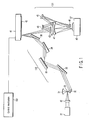
FIG. 1 is a schematic view showing an exposure system according to a first embodiment of the present invention. -
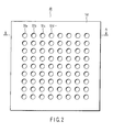
FIG. 2 is a top view of a mask stage according to the first embodiment. -
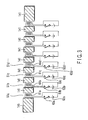
FIG. 3 is a cross-sectional view of the mask stage according to the first embodiment. -
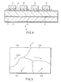
FIG. 4 is a cross-sectional view of a mask according to the first embodiment. -
FIG. 5 is a first schematic view showing a plurality of magnetic domains in the longitudinal section of a magnetostrictive film according to the first embodiment. -
FIG. 6 is a first cross-sectional view of the mask stage and the mask according to the first embodiment. -
FIG. 7 is a first cross-sectional view of the mask stage and the mask according to the first embodiment. -
FIG. 8 is a second schematic view showing a plurality of magnetic domains in the longitudinal section of a magnetostrictive film according to the first embodiment - -
FIG. 9 is a graph showing the characteristics of the magnetostrictive film according to the first embodiment. -
FIG. 10 is a cross-sectional view of a mask for explaining a method of manufacturing the mask according the first embodiment. -
FIG. 11 is a cross-sectional view of the mask of the step succeedingFIG. 10 . -
FIG. 12 is a cross-sectional view of the mask of the step succeedingFIG. 11 . -
FIG. 13 is a cross-sectional view of the mask of the step succeedingFig. 12 . -
FIG. 14 is a cross-sectional view of the mask of the step succeedingFIG. 13 . -
FIG. 15 is a cross-sectional view of the mask of the step succeedingFIG. 14 . -
FIG. 16 is a cross-sectional view of the mask of the step succeedingFIG. 15 . -
FIG. 17 is a cross-sectional view of the mask of the step succeeding FTG. 16. -
FIG. 18 is a cross-sectional view of the mask of the step succeedingFIG. 17 . -
FIG. 19 is a flowchart for explaining a method of manufacturing a semiconductor device according to the first embodiment. -
FIG. 20 is a cross-sectional view of a reflecting mirror according to a second embodiment. - Embodiments of the present invention will be described below with reference to the accompanying drawings. In the description of the following drawings, the same or similar parts are denoted by the same or similar reference symbols. Incidentally, the following embodiments exemplify the devices and methods for embodying the technical idea of the present invention, and the technical idea of the present invention does not specify the arrangements or the like of the constituent components to limit them to the following.
- An optical apparatus according to a first embodiment of the present invention is an exposure system for manufacturing a semiconductor device. As shown in
FIG. 1 , the exposure system includes alight source 31 for emitting light, an illuminationoptical system 130 for propagating light emitted from thelight source 31, and amask stage 41 for holding amask 40 irradiated with the light propagated by the illuminationoptical system 130. - Further, the exposure system includes a projection
optical system 131 for propagating light reflected by themask 40, and awafer stage 48 for holding awafer 57 coated with a resist film to be exposed to the light propagated by the projectionoptical system 131. - The light source emits laser light having wavelengths from the infrared range to the visible range. For example, an yttrium-aluminum-garnet (YAG) laser, excimer laser, or the like by the semiconductor laser excitation is emitted from the
light source 31. - A
condensing lens 32 is arranged adjacent to thelight source 31. Thecondensing lens 32 condenses the laser light emitted from thelight source 31 at afocal point 33. Thefocal point 33 is supplied with xenon (Xe) gas. The Xe gas is brought to a high temperature by being irradiated with laser light. Further, the Xe is excited to a plasmatic state, and when the Xe makes the transition to a low-potential state, EUV light in the soft X-ray range having a wavelength of 12 to 14 nm is released. The released EUV light is condensed by anelliptical mirror 34, and is reflected by aparabolic mirror 35. - The illumination
optical system 130 by which the EUV light reflected by theparabolic mirror 35 is propagated includes reflectingmirrors condenser mirror 38, and a lightpath folding mirror 39. The EUV light is reflected by thereflecting mirrors condenser mirror 38 is reflected by the lightpath folding mirror 39, and then reaches amask 40 fixed to themask stage 41 by the electrostatic attraction force. - The projection
optical system 131 is arranged below themask 40. Further, thewafer stage 48 for holding awafer 57 is arranged below the projectionoptical system 131. The projectionoptical system 131 includes acondenser mirror 47. - The EUV light reflected by the
mask 40 is reflected and condensed by acondenser mirror 42, and is reflected by lightpath folding mirrors condenser mirror 45, and is reflected by a lightpath folding mirror 46. The EUV light reflected by the lightpath folding mirror 46 is reflected and condensed by acondenser mirror 47, and then converges into a focus on a resist film applied to the surface of thewafer 57. The magnification of the projectionoptical system 131 is, for example, 1/4. The EUV light is absorbed into air, and hence it is desirable that the environment of the illuminationoptical system 130, the projectionoptical system 131, and the like be maintained in a vacuum. - As shown in the top view of
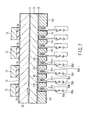
FIG. 2 , themask stage 41 includes asupport body 141 provided with a plurality of openings 51 (51a, 51b, 51c, 51d, ...) in a matrix form. As shown inFIG. 3 which is a cross-sectional view viewed from the A-A direction, a plurality of magnetic field generation parts 61 (61a, 61b, 61c, 61d, ...) are arranged inside the plurality of openings 51. As each of the plurality of magnetic field generation parts 61, a magnetic coil or the like can be used. - A power source 62 (62a, 62b, 62c, 62d, ...) and a switch 63 (63a, 63b, 63c, 63d, ...) are connected to each of the plurality of magnetic field generation parts 61. For example, when the
switch 63a is turned on, a current is supplied from thepower source 62a to the magneticfield generation part 61a, and a magnetic field is generated by the magneticfield generation part 61a. The above applies to the magneticfield generation parts - Each of the plurality of switches 63 and each of the plurality of power sources 62 are connected to a
control mechanism 150 shown inFIG. 1 . Thecontrol mechanism 150 controls opening/closing of each of the plurality of switches 63, and the magnitude of a current supplied by each of the plurality of power sources 62, and controls the magnitude of a magnetic field generated by each of the plurality of magnetic field generation parts 61. - The
mask 40 which is an optical element according to the first embodiment includes, as shown inFIG. 4 , asubstrate 10, amagnetostrictive film 11 which is arranged on thesubstrate 10, the film thickness of the magnetostrictive film varying in accordance with the intensity of the magnetic field, areflection film 12 which is arranged on themagnetostrictive film 11 and reflects EUV light, areflection film 12 which is partly arranged on thereflection film 12 and reflects EUV light, and anabsorption film 15 which is partly arranged on thereflection film 12 and absorbs EUV light. Incidentally, although themagnetostrictive film 11 is arranged between thereflection film 12 and thesubstrate 10, thefilm 11 may be arranged on thereflection film 12. - As a material for the
substrate 10, a low thermal expansion material (LTEM) such as molten silica (Si) doped with titanium (Ti) can be used. As a material for themagnetostrictive film 11, iron group elements such as iron (Fe), cobalt (Co), nickel (Ni), and the like, or lanthanoids such as lanthanum (La), cerium (Ce), praseodymium (Pr), neodymium (Nd), promethium (Pm), samarium (Sm), europium (Eu), thulium (Tm), ytterbium (Yb), and lutetium (Lu), or a Heusler alloy (an alloy containing, for example, Mn, Al, and Cu) can be used. - The
reflection film 12 is a multilayer film formed by alternately accumulating Mo thin films made of molybdenum (Mo) and Si thin films made of silicon (Si) one on top of the other to form a multilayer structure of 40 to 50 layers. For example, the film thickness of an Mo thin film and an Si thin film forming a pair is 6.6 nm. Further, the ratio of the film thickness of the Mo thin film to the film thickness of the paired Mo thin film and the Si thin film is 0.33. - A
protective film 13 for preventing oxidation and the like of thereflection film 12 is arranged on thereflection film 12. As a material for theprotective film 13, Si, ruthenium (Ru) or the like can be used. Anintermediate layer 14 is partly arranged on theprotective film 13. Theintermediate layer 14 is arranged to protect thereflection film 12 and theprotective film 13 from dry etching when theabsorption film 15 is formed on thereflection film 12. - As a material for the
intermediate layer 14, silane oxide (SiO2) and the like can be used. As a material for theabsorption film 15, aluminum (Al), tantalum nitride (TaN), tungsten (W), and the like can be used. Theintermediate layer 14 and theabsorption film 15 are partly arranged on thereflection film 12 to be correspondent to a circuit pattern of the semiconductor device to be manufactured. - Incidentally, the
mask 40 is fixed to themask stage 41 shown inFIG. 1 with the surface on which theabsorption film 15 is arranged directed downward. On the surface of thesubstrate 10 opposite to the surface on which themagnetostrictive film 11 is arranged, aconductive film 16 is arranged. By arranging theconductive film 16 on thesubstrate 10, it becomes possible to fix themask 40 to themask stage 41 by the electrostatic attraction force. - As shown in
FIG. 5 , themagnetostrictive film 11 is constituted of a plurality ofmagnetic domains FIG. 6 , when each of the plurality ofswitches 63a to 63d is opened, no magnetic field is applied to themagnetostrictive film 11. When no magnetic field is applied, the plurality ofmagnetic domains 111a to 111d in the longitudinal section of themagnetostrictive film 11 havevarious magnetization directions 113 as shown inFIG. 5 . - Conversely, for example, in the case where there is a concave part on the undersurface of the
reflection film 12 as shown inFIG. 7 , when theswitch 63a is closed, and a magnetic field is generated by the magneticfield generation part 61a, a magnetic field is applied to a part of themagnetostrictive film 11 above the magneticfield generation part 61a, the film thickness of thefilm 11 varies, and thefilm 11 changes its shape to fill the concave part of the reflection film. - The mechanism which changes the film thickness of the
magnetostrictive film 11 will be described below in more detail. When the magnetic field is applied to themagnetostrictive film 11, themagnetization directions 113 of the plurality ofmagnetic domains 111a to 111d are made uniform so as to be coincident with thedirection 115 of the magnetic field as shown inFIG. 8 . Accordingly, each of the plurality ofmagnetic domains direction 115 of the magnetic field. Assuming that the film thickness of themagnetostrictive film 11 in the case where no magnetic field is applied is t, and an increment in the film thickness of a part of themagnetostrictive film 11 to which the magnetic field is applied is Δt, the relationship between the magnetic field and the increment Δt in the film thickness t of themagnetostrictive film 11 is given byFIG. 9 . - When light is absorbed into the
absorption film 15 and thereflection film 12 of the mask shown inFIG. 4 , the film thicknesses of theabsorption film 15 and thereflection film 12 are changed by the thermal expansion, and the height position of theabsorption film 15 is changed. When the height position of theabsorption film 15 is changed, the position of the projection image of themask 40 on thewafer 57 shown inFIG. 1 is deviated, and a manufacturing error of the semiconductor device is caused. Further, when the film thicknesses of theabsorption film 15 and thereflection film 12 are changed by the thermal expansion, an aberration or flare is caused in the projectionoptical system 131 shown inFIG. 1 in some cases. - Further, when the
substrate 10 of themask 40 is not flat because of a defect or the like, or when thesupport body 141 of themask stage 41 is curved, or when there are particles such as dust or the like between themask 40 and themask stage 41, too, the image on themask 40 on thewafer 57 shown inFIG. 1 is shifted. - Conversely, the film thickness of the
magnetostrictive film 11 of themask 40 shown inFIG. 6 can be partly expanded or contracted by each of the plurality of magneticfield generation parts 61a to 61d of the exposure system. Therefore, even when theabsorption film 15 or thereflection film 12 is thermally expanded, it becomes possible to correct the position of thereflection film 12 or correct the aberration of the projectionoptical system 131. Thus, it becomes possible to correct the positional deviation of the projection image of themask 40 on thewafer 57 shown inFIG. 1 or correct distortion of the projection image caused by the aberration. - Further, the film thickness of the
magnetostrictive film 11 of themask 40 shown inFIG. 6 is not controlled by mechanical drive, and is controlled by magnetic fields generated by the plurality of magnetic field generation parts 61. Accordingly, it becomes possible to easily control the film thickness of themagnetostrictive film 11 even in a vacuum without causing crosstalk. - Furthermore, the plurality of magnetic field generation parts 61 are provided in the mask stage, and hence it is not necessary to provide the
mask 40 with a complicated mechanism for controlling the film thickness other than themagnetostrictive film 11. It is also unnecessary to provide electric wiring or mechanical connection between themask 40 and themask stage 41. Accordingly, it becomes possible to hold down the manufacturing cost of the semiconductor device. Although in the manufacturing job site of the semiconductor device, replacement of the mask is frequently performed, the manufacturing cost of the semiconductor device can be held down by using themask 40 according to this embodiment. - Next, with reference to
FIGS. 10 to 18 , the method of manufacturing the mask according to this embodiment will be described below. - (a) First, a
substrate 10 shown inFIG. 10 having a firstprincipal surface 101 and a secondprincipal surface 102 opposed to the first principal surface is prepared. Then, aconductive film 16 is formed on the secondprincipal surface 102 of thesubstrate 10 by a vapor deposition method or the like. Thereafter, amagnetostrictive film 11 manufactured by a powder metallurgical process or the like is prepared, and themagnetostrictive film 11 is brought into close contact with the firstprincipal surface 101 of thesubstrate 10 as shown inFIG. 11 . - (b) As shown in
FIG. 12 , an Si thin film is formed on themagnetostrictive film 11 by the magnetron sputtering method in an argon (Ar) gas environment by using an Si target. Then, an Mo thin film is formed on the Si thin film in the Ar gas environment by using an Mo target. Thereafter, formation of an Mo thin film and formation of an Si thin film are alternately repeated, thereby forming areflection film 12 on themagnetostrictive film 11. Thereafter, aprotective film 13 shown inFIG. 13 is formed on thereflection film 12 in the Ar gas environment by using an Si target. - (c) As shown in
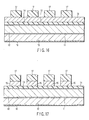
FIG. 14 , SiO2 is deposited on theprotective film 13 by the chemical vapor deposition (CVD) method or the like, thereby forming anintermediate layer 14. Then, as shown inFIG, 15 , Al is accumulated on theintermediate layer 14 by the sputtering method or the like, thereby forming anabsorption film 15. As shown inFIG. 16 , theabsorption film 15 is coated with a resist film by spin coating, an opening pattern is provided on the resist film by the lithography method or the like, thereby forming anetching mask 17 on theabsorption film 15. - (d) As shown in
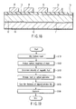
FIG. 17 , a plurality parts of theabsorption film 15 exposed to the outside from theetching mask 17 are selectively removed by the dry etching method or the like using Ar gas. At this time, theprotective film 13 is protected by the intermediate layer 14- Thereafter, theetching mask 17 is removed from the surface of theabsorption film 15 by the ashing method or the like. As shown inFIG. 18 , by using theabsorption film 15 from which the plural parts have already been selectively removed as a mask, the exposed parts of theintermediate layer 14 are selectively removed by the anithotropic etching method or the like, thereby completing themask 40 shown inFIG. 4 . - Next, the method of manufacturing the semiconductor device according to this embodiment will be described below with reference to the flowchart of
FIG. 19 . - (a) In step S101, in accordance with the procedures described previously with reference to
FIGS. 10 to 18 , themask 40 shown inFIG. 4 is manufactured. In step S102, the surface roughness of theabsorption film 15 and theprotective film 13 of themask 40 is analyzed by using a surface analyzer such as a scanning electron microscope (SEM), an atomic force microscope (AFM), and the like. When there is a protrusion or a recess having a size exceeding the permissible value on theabsorption film 15 and theprotective film 13, the size of the protrusuion or the recess is measured by the surface analyzer. - (b) In step S103, the intensity of the magnetic field to be applied to the
magnetostrictive film 11 in order to correct the protrusion or the recess of theabsorption film 15 and theprotective film 13 is determined by using the relationship between the magnetic field and the amount of variation in the film thickness of themagnetostrictive film 11 which is shown inFIG. 9 , and is obtained in advance. Then, in step S104, themask 40 is fixed to themask stage 41 of the exposure system as shown inFIG. 6 . - (c) In step S105, the
control mechanism 150 shown inFIG. 1 controls opening/closing of each of the plurality of switches 63 shown inFIG. 6 in such a manner that a magnetic field generation part of the plural magnetic field generation parts 61 in the vicinity of the protrusion or the recess of theabsorption film 15 and theprotective film 13 generates a magnetic field. Further, thecontrol mechanism 150 shown inFIG. 1 controls the magnitude of a current supplied to each of the plural magnetic field generation parts 61 from each of the plural power sources 62 shown inFIG. 6 in such a manner that the magnetic field having the intensity determined in step S103 is generated. By applying the magnetic field to themagnetostrictive film 11, the film thickness of themagnetostrictive film 11 is varied, thereby correcting the protrusion or the recess of theabsorption film 15 and theprotective film 13. - (d) In step S106, a
wafer 57 coated with a resist film by spin coating is arranged on thewafer stage 48 shown inFIG. 1 . Then, laser light is emitted from thelight source 31, and themask 40 is irradiated with EUV light generated at thefocal point 33 in the Xe gas environment. The EUV light reflected by themask 40 forms a projection image of themask 40 on thewafer 57 through the projectionoptical system 131. Thereafter, through a development process of the resist film, the wiring step, and the like, the semiconductor device is completed. - Incidentally, the thermal expansion of the
reflection film 12 of themask 40 may be predicted by a simulation or the like in step S102 ofFIG. 19 , and a magnetic field may be applied to themagnetostrictive film 11 to correct the thermal expansion of thereflection film 12 in step S105. - According to the method of manufacturing the semiconductor device shown above, even when a protrusion or a recess is present in the
absorption film 13, theprotective film 13, or thereflection film 12, it becomes possible to correct the protrusion or the recess of theabsorption film 15 and theprotective film 13 by controlling the film thickness of themagnetostrictive film 11. Accordingly, it becomes possible to make the allowable range of the surface roughness of theabsorption film 15 and theprotective film 13 wide at the time of manufacturing themask 40. Therefore, it becomes possible to reduce the manufacturing cost of themask 40, and improve the manufacturing yield of themask 40. - Further, the
substrate 10 of themask 40 shown inFIG. 6 is not always flat, and is curved in some cases. Further, there are cases where a plurality ofmasks 40 corresponding to different circuit patterns are manufactured, and themask 40 on themask stage 41 is successively replaced with another to thereby manufacture a semiconductor device. However, the degrees of the curved states ofsubstrates 10 of a plurality of masks do not coincide with each other in some cases. However, when the degree of the curved state of thesubstrate 10 or thesupport body 141 is also measured in step S102 ofFIG. 19 , and a magnetic field is applied to themagnetostrictive film 11 so that the curve can be corrected in step S105, it becomes possible to form a projection image equivalent to the projection image obtained by using a just designedmask 40 on thewafer 57 shown inFIG. 1 . - In the first embodiment, although the
mask 40 shown inFIG. 4 has been described as an optical element provided with a magnetostrictive film, an optical element provided with a magnetostrictive film can also be applied to, for example, a reflectingmirror 36 shown inFIG. 1 .FIG. 20 is a schematic view showing the configuration of a reflecting mirror (device) according to a second embodiment of the present invention. - As shown in
FIG. 20 , a reflectingmirror 36 according to the second embodiment includes asubstrate 110, amagnetostrictive film 211 arranged on thesubstrate 110, and areflection film 112 arranged on themagnetostrictive film 211. The reflectingmirror 36 further includes aconductive film 116 on the underside thereof, and is fixed to a reflectingmirror stage 341 by the electrostatic attraction force or the like. Incidentally, although themagnetostrictive film 211 is arranged between thereflection film 112 and thesubstrate 110, thefilm 211 may be arranged in thereflection film 112. - The reflecting
mirror stage 341 includes, as in the case of the first embodiment, asupport body 241 provided with a plurality of openings, a plurality of magnetic field generation parts 161 (161a, 161b, 161c, 161d, . . .) inserted in the plurality of openings of thesupport body 241, a plurality of power sources 162 (162a, 162b, 162c, 162d, ...) connected to the plurality of magnetic field generation parts 161, and a plurality of switches 163 (163a, 163b, 163c, 163d, ...) each of which is arranged between each of the plurality of magnetic field generation parts 161 and each of the plurality of power sources 162 to be connected to the corresponding magnetic field generation part 161 and the corresponding power source 162. - For example, when an aberration or flare is caused in the projection
optical system 131 shown inFIG. 1 , a magnetic field is generated by each of the plurality of magnetic field generation parts 161 shown inFIG. 20 to adjust the film thickness of themagnetostrictive film 211 of the reflectingmirror 36, whereby the aberration or falare can be removed. - As described above, according to the second embodiment, it is possible to provide a reflecting mirror capable of controlling the surface roughness with a high degree of accuracy.
- In the embodiments described above, although the exposure system and the reflecting mirror have been described as the optical apparatus, besides the present invention can be applied to an optical microscope, a hologram formation apparatus, and the like.
Claims (20)
- An optical element characterized by comprising:a substrate;a magnetostrictive film which is arranged on the substrate, a film thickness of the magnetostrictive film varying in accordance with intensity of a magnetic field; anda reflection film which is arranged on the magnetostrictive film and reflects light.
- The optical element according to claim 1, characterized in that the substrate is formed of a material that transmits the light.
- The optical element according to any one of claims 1 to 2, characterized in that the magnetostrictive film includes at least one of Fe, Co, Ni, La, Ce, Pr, Nd, Pm, Sm, Eu, Gd, Tb, Dy, Ho, Er, Tm, Yb, Lu, Mn, Al, and Cu.
- The optical element according to any one of claims 1 to 3, characterized in that the reflection film is a multilayer film formed by alternately accumulating Mo thin films and Si thin films one on top of the other.
- The optical element according to any one of claims 1 to 4, characterized by further comprising an absorption film selectively formed on the reflection film and absorbing the light.
- The optical element according to claim 5, characterized in that the absorption film forms a mask pattern.
- The optical element according to claim 5 or 6, characterized in that the absorption film is formed of one of Al, TaN, and W.
- The optical element according to any one of claims 5 to 7, characterized by further comprising a first protective film and a second protective film formed between the reflection film and the absorption film.
- The optical element according to claim 8, characterized in that the first protective film is formed of Si or Ru.
- The optical element according to claim 8, characterized in that the second protective film is formed of SiO2.
- An optical apparatus characterized by comprising:a stage including a holder provided with a plurality of holes arranged in a carrying surface thereof for carrying an optical element provided with a magnetostrictive film which is arranged on a substrate, a film thickness of the magnetostrictive film varying in accordance with intensity of a magnetic field, and a reflection film arranged on the magnetostrictive film and reflecting light;a plurality of magnetic field generation parts embedded in the plurality of holes of the holder; anda control mechanism for controlling the magnetic field generated by each of the plurality of magnetic field generation parts, and controlling the film thickness of the magnetostrictive film of the optical element.
- The optical apparatus according to claim 11, characterized in that each of the plurality of magnetic field generation parts includes a coil, a power source, and a switch.
- The optical apparatus according to claim 11 or 12, characterized in that the control mechanism selectively drives the plurality of magnetic field generation parts by using the switches, changes the magnetic field generated by the coil by controlling the power source of a selected one of the magnetic field generation parts, and controls the film thickness of the magnetostrictive film of the optical element.
- The optical apparatus according to any one of claims 11 to 13, characterized in that the plurality of holes provided in the holder are provided in a form of a matrix.
- The optical apparatus according to any one of claims 11 to 14, characterized by further comprising:a light source;an illumination optical system for generating conversion light from the light source, and irradiating the optical element with the conversion light; anda projection optical system for projecting reflected light from the optical element on an object.
- The optical apparatus according to claim 15, characterized in that the light source is a light source for emitting laser light.
- The optical apparatus according to claim 15 or 16, characterized in that the illumination optical system includes a reflection optical system.
- The optical apparatus according to any one of claims 15 to 17, characterized in that the illumination optical system generates extreme ultraviolet light by using the laser light.
- The optical apparatus according to any one of claims 15 to 18, characterized in that the projection optical system includes the reflection optical system.
- The optical apparatus according to any one of claims 11 to 19, characterized in that the magnetostrictive film includes at least one of Fe, Co, Ni, La, Ce, Pr, Nd, Pm, Sm, Eu, Gd, Tb, Dy, Ho, Er, Tm, Yb, Lu, Mn, Al, and Cu.
Applications Claiming Priority (2)
| Application Number | Priority Date | Filing Date | Title |
|---|---|---|---|
| JP2006162072A JP2007335444A (en) | 2006-06-12 | 2006-06-12 | Optical element and optical device |
| PCT/JP2007/058650 WO2007145025A1 (en) | 2006-06-12 | 2007-04-20 | Optical element and optical device |
Publications (1)
| Publication Number | Publication Date |
|---|---|
| EP2028522A1 true EP2028522A1 (en) | 2009-02-25 |
Family
ID=38831545
Family Applications (1)
| Application Number | Title | Priority Date | Filing Date |
|---|---|---|---|
| EP07742085A Withdrawn EP2028522A1 (en) | 2006-06-12 | 2007-04-20 | Optical element and optical device |
Country Status (6)
| Country | Link |
|---|---|
| US (1) | US20090141378A1 (en) |
| EP (1) | EP2028522A1 (en) |
| JP (1) | JP2007335444A (en) |
| KR (1) | KR20090007432A (en) |
| TW (1) | TW200809423A (en) |
| WO (1) | WO2007145025A1 (en) |
Cited By (3)
| Publication number | Priority date | Publication date | Assignee | Title |
|---|---|---|---|---|
| EP2263255A1 (en) * | 2008-03-07 | 2010-12-22 | Nederlandse Organisatie voor toegepast -natuurwetenschappelijk onderzoek TNO | Process for adjusting the coefficient of friction and/or adhesion between surfaces of two solid objects |
| CN103235410A (en) * | 2013-03-29 | 2013-08-07 | 上海大学 | Magnetofluid deformable mirror device |
| WO2016087092A1 (en) * | 2014-12-02 | 2016-06-09 | Carl Zeiss Smt Gmbh | Surface correction on coated reflective optical elements |
Families Citing this family (5)
| Publication number | Priority date | Publication date | Assignee | Title |
|---|---|---|---|---|
| US7843632B2 (en) * | 2006-08-16 | 2010-11-30 | Cymer, Inc. | EUV optics |
| DE102012207003A1 (en) * | 2012-04-27 | 2013-10-31 | Carl Zeiss Smt Gmbh | Optical elements with magnetostrictive material |
| US20150090905A1 (en) * | 2013-09-27 | 2015-04-02 | Dmitri E. Nikonov | Micromagnet Based Extreme Ultra-Violet Radiation Source |
| JP6862154B2 (en) * | 2016-11-22 | 2021-04-21 | キヤノン株式会社 | Manufacturing methods for optics, exposure equipment, and articles |
| JP7122919B2 (en) * | 2018-09-21 | 2022-08-22 | マクセル株式会社 | Information display device and reflecting mirror used therefor |
Family Cites Families (9)
| Publication number | Priority date | Publication date | Assignee | Title |
|---|---|---|---|---|
| JPH02168614A (en) * | 1988-09-27 | 1990-06-28 | Mitsubishi Electric Corp | Mask for x-ray exposure and exposing method using same |
| US4877283A (en) * | 1988-09-28 | 1989-10-31 | Little Johnny L | Flexible cover and system for enclosing automobile hatch |
| US5767507A (en) * | 1996-07-15 | 1998-06-16 | Trustees Of Boston University | Polarization sensitive photodetectors and detector arrays |
| US5958631A (en) * | 1998-02-17 | 1999-09-28 | International Business Machines Corporation | X-ray mask structure |
| US6377655B1 (en) * | 1998-05-08 | 2002-04-23 | Nikon Corporation | Reflective mirror for soft x-ray exposure apparatus |
| JP2003015060A (en) * | 2001-06-28 | 2003-01-15 | Hitachi Maxell Ltd | Light switch |
| US20030234993A1 (en) * | 2002-06-21 | 2003-12-25 | Hazelton Andrew J. | Adaptive optic off-axis metrology |
| US6880942B2 (en) * | 2002-06-20 | 2005-04-19 | Nikon Corporation | Adaptive optic with discrete actuators for continuous deformation of a deformable mirror system |
| JP2004056125A (en) | 2002-06-20 | 2004-02-19 | Nikon Corp | Reflection projection optical system with individual actuator |
-
2006
- 2006-06-12 JP JP2006162072A patent/JP2007335444A/en not_active Abandoned
-
2007
- 2007-04-20 WO PCT/JP2007/058650 patent/WO2007145025A1/en not_active Ceased
- 2007-04-20 KR KR1020087027754A patent/KR20090007432A/en not_active Ceased
- 2007-04-20 EP EP07742085A patent/EP2028522A1/en not_active Withdrawn
- 2007-04-25 TW TW096114625A patent/TW200809423A/en unknown
-
2008
- 2008-12-11 US US12/332,628 patent/US20090141378A1/en not_active Abandoned
Non-Patent Citations (1)
| Title |
|---|
| See references of WO2007145025A1 * |
Cited By (4)
| Publication number | Priority date | Publication date | Assignee | Title |
|---|---|---|---|---|
| EP2263255A1 (en) * | 2008-03-07 | 2010-12-22 | Nederlandse Organisatie voor toegepast -natuurwetenschappelijk onderzoek TNO | Process for adjusting the coefficient of friction and/or adhesion between surfaces of two solid objects |
| CN103235410A (en) * | 2013-03-29 | 2013-08-07 | 上海大学 | Magnetofluid deformable mirror device |
| WO2016087092A1 (en) * | 2014-12-02 | 2016-06-09 | Carl Zeiss Smt Gmbh | Surface correction on coated reflective optical elements |
| CN107111015A (en) * | 2014-12-02 | 2017-08-29 | 卡尔蔡司Smt有限责任公司 | Surface correction on the reflective optical devices of coating |
Also Published As
| Publication number | Publication date |
|---|---|
| KR20090007432A (en) | 2009-01-16 |
| TW200809423A (en) | 2008-02-16 |
| WO2007145025A1 (en) | 2007-12-21 |
| JP2007335444A (en) | 2007-12-27 |
| US20090141378A1 (en) | 2009-06-04 |
Similar Documents
| Publication | Publication Date | Title |
|---|---|---|
| US20090141378A1 (en) | Optical element and optical apparatus | |
| CN109946919B (en) | EUV mask blank and photomask | |
| JP5406602B2 (en) | Multilayer mirror and lithographic apparatus | |
| JP4174970B2 (en) | Laser-excited plasma light source, exposure apparatus, manufacturing method thereof, and device manufacturing method | |
| US7948675B2 (en) | Surface-corrected multilayer-film mirrors with protected reflective surfaces, exposure systems comprising same, and associated methods | |
| EP1333323A2 (en) | Self-cleaning reflective optical elements for use in x-ray optical systems, and optical systems and microlithography systems comprising same | |
| US8329361B2 (en) | Reflective mask blank, method of manufacturing a reflective mask blank and method of manufacturing a reflective mask | |
| US6909774B2 (en) | Apparatus and methods for surficial milling of selected regions on surfaces of multilayer-film reflective mirrors as used in X-ray optical systems | |
| US20090141356A1 (en) | Optical element, and light source unit and exposure apparatus having the same | |
| US20100119981A1 (en) | Passivation of Multi-Layer Mirror for Extreme Ultraviolet Lithography | |
| KR101790074B1 (en) | Radiation source, lithographic apparatus and device manufacturing method | |
| CN117348336A (en) | Pellicle, method for preparing pellicle, dynamic airlock and lithography equipment | |
| JP2004531905A (en) | Repair of amplitude defects in multilayer coatings | |
| JP2002299228A (en) | Reticle, exposure apparatus and exposure method using the same | |
| JP6144874B2 (en) | Reflective optical component and device manufacturing method for a lithographic apparatus | |
| EP0671658A2 (en) | Exposure apparatus and reflection type mask to be used in the same | |
| CN114355721A (en) | Method of manufacturing Extreme Ultraviolet (EUV) photomask and method and apparatus for correcting EUV photomask | |
| JP5715134B2 (en) | Spectral purity filter and method of manufacturing spectral purity filter | |
| JP4567659B2 (en) | Lithogfi apparatus and device manufacturing method | |
| KR101625934B1 (en) | Multilayer mirror and lithographic apparatus | |
| JP2000286191A (en) | Exposure apparatus, exposure method, and device manufacturing method | |
| JP4705843B2 (en) | Lithographic apparatus and device manufacturing method | |
| TW200809833A (en) | An aperture changing apparatus and method | |
| JP3662571B2 (en) | Lithographic apparatus and device manufacturing method | |
| JP2004153279A (en) | Lithographic apparatus and device manufacturing method |
Legal Events
| Date | Code | Title | Description |
|---|---|---|---|
| PUAI | Public reference made under article 153(3) epc to a published international application that has entered the european phase |
Free format text: ORIGINAL CODE: 0009012 |
|
| 17P | Request for examination filed |
Effective date: 20081209 |
|
| AK | Designated contracting states |
Kind code of ref document: A1 Designated state(s): AT BE BG CH CY CZ DE DK EE ES FI FR GB GR HU IE IS IT LI LT LU LV MC MT NL PL PT RO SE SI SK TR |
|
| AX | Request for extension of the european patent |
Extension state: AL BA HR MK RS |
|
| RIN1 | Information on inventor provided before grant (corrected) |
Inventor name: HIGASHIKAWA, IWAO Inventor name: HIGASHIKI, TATSUHIKO Inventor name: TAWARAYAMA, KAZUO |
|
| REG | Reference to a national code |
Ref country code: DE Ref legal event code: 8566 |
|
| DAX | Request for extension of the european patent (deleted) | ||
| RBV | Designated contracting states (corrected) |
Designated state(s): NL |
|
| STAA | Information on the status of an ep patent application or granted ep patent |
Free format text: STATUS: THE APPLICATION HAS BEEN WITHDRAWN |
|
| 18W | Application withdrawn |
Effective date: 20120207 |