EP2023697A1 - Wiring board - Google Patents
Wiring board Download PDFInfo
- Publication number
- EP2023697A1 EP2023697A1 EP07744278A EP07744278A EP2023697A1 EP 2023697 A1 EP2023697 A1 EP 2023697A1 EP 07744278 A EP07744278 A EP 07744278A EP 07744278 A EP07744278 A EP 07744278A EP 2023697 A1 EP2023697 A1 EP 2023697A1
- Authority
- EP
- European Patent Office
- Prior art keywords
- wiring substrate
- conductive
- insulating layer
- substrate
- wiring
- Prior art date
- Legal status (The legal status is an assumption and is not a legal conclusion. Google has not performed a legal analysis and makes no representation as to the accuracy of the status listed.)
- Withdrawn
Links
Images



Classifications
-
- H—ELECTRICITY
- H05—ELECTRIC TECHNIQUES NOT OTHERWISE PROVIDED FOR
- H05K—PRINTED CIRCUITS; CASINGS OR CONSTRUCTIONAL DETAILS OF ELECTRIC APPARATUS; MANUFACTURE OF ASSEMBLAGES OF ELECTRICAL COMPONENTS
- H05K1/00—Printed circuits
- H05K1/02—Details
- H05K1/11—Printed elements for providing electric connections to or between printed circuits
-
- H—ELECTRICITY
- H05—ELECTRIC TECHNIQUES NOT OTHERWISE PROVIDED FOR
- H05K—PRINTED CIRCUITS; CASINGS OR CONSTRUCTIONAL DETAILS OF ELECTRIC APPARATUS; MANUFACTURE OF ASSEMBLAGES OF ELECTRICAL COMPONENTS
- H05K1/00—Printed circuits
- H05K1/02—Details
- H05K1/11—Printed elements for providing electric connections to or between printed circuits
- H05K1/117—Pads along the edge of rigid circuit boards, e.g. for pluggable connectors
-
- H—ELECTRICITY
- H01—ELECTRIC ELEMENTS
- H01R—ELECTRICALLY-CONDUCTIVE CONNECTIONS; STRUCTURAL ASSOCIATIONS OF A PLURALITY OF MUTUALLY-INSULATED ELECTRICAL CONNECTING ELEMENTS; COUPLING DEVICES; CURRENT COLLECTORS
- H01R12/00—Structural associations of a plurality of mutually-insulated electrical connecting elements, specially adapted for printed circuits, e.g. printed circuit boards [PCB], flat or ribbon cables, or like generally planar structures, e.g. terminal strips, terminal blocks; Coupling devices specially adapted for printed circuits, flat or ribbon cables, or like generally planar structures; Terminals specially adapted for contact with, or insertion into, printed circuits, flat or ribbon cables, or like generally planar structures
- H01R12/50—Fixed connections
-
- H—ELECTRICITY
- H05—ELECTRIC TECHNIQUES NOT OTHERWISE PROVIDED FOR
- H05K—PRINTED CIRCUITS; CASINGS OR CONSTRUCTIONAL DETAILS OF ELECTRIC APPARATUS; MANUFACTURE OF ASSEMBLAGES OF ELECTRICAL COMPONENTS
- H05K3/00—Apparatus or processes for manufacturing printed circuits
- H05K3/22—Secondary treatment of printed circuits
- H05K3/24—Reinforcing of the conductive pattern
- H05K3/245—Reinforcing conductive patterns made by printing techniques or by other techniques for applying conductive pastes, inks or powders; Reinforcing other conductive patterns by such techniques
- H05K3/247—Finish coating of conductors by using conductive pastes, inks or powders
-
- H—ELECTRICITY
- H05—ELECTRIC TECHNIQUES NOT OTHERWISE PROVIDED FOR
- H05K—PRINTED CIRCUITS; CASINGS OR CONSTRUCTIONAL DETAILS OF ELECTRIC APPARATUS; MANUFACTURE OF ASSEMBLAGES OF ELECTRICAL COMPONENTS
- H05K1/00—Printed circuits
- H05K1/02—Details
- H05K1/09—Use of materials for the conductive, e.g. metallic pattern
- H05K1/092—Dispersed materials, e.g. conductive pastes or inks
- H05K1/095—Dispersed materials, e.g. conductive pastes or inks for polymer thick films, i.e. having a permanent organic polymeric binder
-
- H—ELECTRICITY
- H05—ELECTRIC TECHNIQUES NOT OTHERWISE PROVIDED FOR
- H05K—PRINTED CIRCUITS; CASINGS OR CONSTRUCTIONAL DETAILS OF ELECTRIC APPARATUS; MANUFACTURE OF ASSEMBLAGES OF ELECTRICAL COMPONENTS
- H05K2201/00—Indexing scheme relating to printed circuits covered by H05K1/00
- H05K2201/03—Conductive materials
- H05K2201/0332—Structure of the conductor
- H05K2201/0335—Layered conductors or foils
- H05K2201/035—Paste overlayer, i.e. conductive paste or solder paste over conductive layer
-
- H—ELECTRICITY
- H05—ELECTRIC TECHNIQUES NOT OTHERWISE PROVIDED FOR
- H05K—PRINTED CIRCUITS; CASINGS OR CONSTRUCTIONAL DETAILS OF ELECTRIC APPARATUS; MANUFACTURE OF ASSEMBLAGES OF ELECTRICAL COMPONENTS
- H05K2201/00—Indexing scheme relating to printed circuits covered by H05K1/00
- H05K2201/07—Electric details
- H05K2201/0753—Insulation
- H05K2201/0769—Anti metal-migration, e.g. avoiding tin whisker growth
-
- H—ELECTRICITY
- H05—ELECTRIC TECHNIQUES NOT OTHERWISE PROVIDED FOR
- H05K—PRINTED CIRCUITS; CASINGS OR CONSTRUCTIONAL DETAILS OF ELECTRIC APPARATUS; MANUFACTURE OF ASSEMBLAGES OF ELECTRICAL COMPONENTS
- H05K2201/00—Indexing scheme relating to printed circuits covered by H05K1/00
- H05K2201/09—Shape and layout
- H05K2201/09209—Shape and layout details of conductors
- H05K2201/09372—Pads and lands
- H05K2201/09436—Pads or lands on permanent coating which covers the other conductors
-
- H—ELECTRICITY
- H05—ELECTRIC TECHNIQUES NOT OTHERWISE PROVIDED FOR
- H05K—PRINTED CIRCUITS; CASINGS OR CONSTRUCTIONAL DETAILS OF ELECTRIC APPARATUS; MANUFACTURE OF ASSEMBLAGES OF ELECTRICAL COMPONENTS
- H05K2201/00—Indexing scheme relating to printed circuits covered by H05K1/00
- H05K2201/09—Shape and layout
- H05K2201/09209—Shape and layout details of conductors
- H05K2201/09654—Shape and layout details of conductors covering at least two types of conductors provided for in H05K2201/09218 - H05K2201/095
- H05K2201/09709—Staggered pads, lands or terminals; Parallel conductors in different planes
-
- H—ELECTRICITY
- H05—ELECTRIC TECHNIQUES NOT OTHERWISE PROVIDED FOR
- H05K—PRINTED CIRCUITS; CASINGS OR CONSTRUCTIONAL DETAILS OF ELECTRIC APPARATUS; MANUFACTURE OF ASSEMBLAGES OF ELECTRICAL COMPONENTS
- H05K3/00—Apparatus or processes for manufacturing printed circuits
- H05K3/22—Secondary treatment of printed circuits
- H05K3/28—Applying non-metallic protective coatings
Definitions
- the present invention relates to a wiring substrate that is provided with a fitting portion for connection with a connector.
- a fitting portion for connecting a wiring substrate with a connector of another device conventionally has a structure in which a portion of conductive circuits that are formed on one surface of the substrate are exposed, with contact points of the connector side brought into contact with the exposed portions of the conductive circuits to be electrically connected, as shown in FIG. 8A and FIG. 8B .
- the fitting portion of this wiring substrate in addition to reducing the diameter of the connection by miniaturization and thinning of the device, fine pitching of the conductive circuits is increasingly progressing.
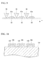
- a covering layer 105 that is formed by coating a migration resistant resin (a paste material) on the outer periphery of a printed circuit portion 102 that is formed on the upper surface of a wiring substrate 101 in order to suppress migration resistance, as shown in FIG. 10 .
- a migration resistant resin a paste material
- FIG. 10 In the case of this substrate structure, when fine pitching is performed, due to the accuracy of the printing, there is a risk of the side surface portion of the printed circuit being exposed because a sufficient covering layer cannot be formed. When the printing circuit is exposed, migration readily occurs, which becomes an impediment to fine pitching.
- the present invention was achieved in view of the above circumstances, and has as its object to provide a wiring substrate that is provided with a fitting portion that can prevent electrical faults between conductive circuits and is compatible with a fine pitch structure without impairing the fitting with a connector.
- the wiring substrate according to one aspect of the present invention is a wiring substrate that is provided with a fitting portion for connection with a connector, characterized in that the wiring substrate includes a substrate; a plurality of conductive circuits that are arranged in parallel on one surface of the substrate; an insulating layer that covers the conductive circuits; opening portions that are provided in the insulating layer at the fitting portion and expose at least a portion of the conductive circuits; and a plurality of electrodes that are disposed on the exposed conductive circuits through the opening portion and consist of a conductive member; at least one among the electrodes being disposed so as to cover the exposed portion of the conductive circuit and a portion of the insulating layer in the wiring width direction of the conductive circuit.
- the electrode contains a member that has migration resistance. Also, it is preferable that each electrode covers the entirety of a corresponding opening portion. Further, it is preferable that the surface of the insulating layer portion that is partially covered by each electrode has a tapered shape. Still further, it is preferable that the upper surface of the electrodes is the same height as or higher than the upper surface of the insulating layer. Even still further, it is preferable that the electrodes are disposed in an approximate line when the substrate is viewed in plane view. Separately, it is preferable that the electrodes are disposed in a staggered shape when the substrate is viewed in plane view.
- the wiring substrate of the present invention it is possible to sufficiently maintain a fitting with a connector. Also, since an insulating layer is provided between conductive circuits, it is possible to suppress electrical faults between adjacent conductive circuits and possible to form a fitting portion with a fine pitching structure.
- FIG. 1 is a perspective view of the fitting portion vicinity in the wiring substrate of one embodiment of the present invention.
- FIG. 2A is a sectional view along line A-A of FIG. 1 .
- a wiring substrate 10 of the present embodiment is provided with a substrate 11, a conductive circuit 12 that is formed on one surface 11 a of this substrate 11, and an insulating layer 13 that covers this conductive circuit 12.
- a fitting portion 14 is formed that fits with a connector 21 such as another device.
- an opening portion 18 is formed that exposes a portion of the conductive circuit 12 so as to partition an individual conductive circuit 12 to the insulating layer 13.
- a portion of the conductive circuit 12 is exposed from the insulating layer 13 as an exposed surface 12a.
- an electrode layer 15 that consists of a conductive member is formed on the exposed surface 12a of this conductive circuit 12.
- This electrode layer 15 makes contact with the conductive circuit 12 at its lower surface, while the upper surface thereof is extended so as to also cover a portion of the insulating layer 13 in the wiring width direction W of the conductive circuit 12.
- an electrode width L2 in the wiring width direction W of the upper surface of the electrode layer 15 is greater than a wiring width L1 of the conductive circuit 12.
- a plurality of conductive circuits 23 are opened so as to be individually exposed on a substrate 24, and an insulating layer 22 is formed between the opening portions of the mutually adjacent conductive circuits 23, 23. Thereby, even if the formation interval of the conductive circuits 23 is reduced by fine pitching, it is possible to eliminate electrical malfunctions in the conductive circuits 23, 23.
- the electrode layer 15 may have a constitution that covers the entire opening portion 18 or only a portion thereof. Also, a surface 13a of the insulating layer 13 at the portion that is partially covered by the electrode layer 15 is preferably formed in a tapered shape. If the surface 13a of the insulating layer 13 is formed in a tapered shaped, when the electrode layer 15 is applied using a conductive paste, it is possible to achieve a flattening of the upper surface of the electrode layer 15 by the conductive paste flowing between adjacent insulating layers 13, and so improve the connectability with the connector.
- the upper surface of the electrode layer 15 is formed so as to be the same height as the upper surface of the insulating layer 13 or higher. Thereby, during attachment and removal of the connector to/from the fitting portion, when the connector hits the upper surface of the insulating layer 13, it is possible to prevent damage to the insulating layer 13 due to scraping of the insulating layer 13, which is formed with a soft material such as resin or the like, and the loss of insulation performance. Also, if the height of the upper surface of the electrode layer 15 is made to be the same height as the upper surface of the insulating layer 13, the fitting with the connector is improved, and so it is possible to more reliably achieve conduction with the connector.
- the connector does not hit the soft insulating layer 13, which proves useful for maintaining the insulation performance by protecting the insulating layer 13.
- the substrate 10 be an electrically insulating substrate made of resin.
- This kind of substrate 10 constitutes a connection wiring substrate with the connector that is connected to the flexible substrate.
- the conductive circuit 12 is a conductor that includes Ag or Cu from the point of low material cost and low resistance. It is preferable that this conductive circuit 12 be formed by applying a conductive paste that includes for example Ag or Cu on the substrate 10 in a predetermined pattern. When applying this conductive paste, a method such as screen printing or ink jet printing may be used from the standpoint of lowering cost.
- the insulating layer 13 be formed from an insulating resin, such as polyester resin, polyurethane resin, phenol resin, epoxy resin and the like. It is preferable that this resin with an insulating performance is printed by a method such as screen printing as an insulating paste that includes a solvent, but is not limited thereto.
- the electrode layer 15 uses a material with a conductivity that is as low as possible. If constituted from such a member, even if the distance between the conductive circuit 12 and the connector 21 separates due to a shift of the connector 21, it is possible to enable a low electrical resistance via the electrode layer 15.
- a method of forming the electrode layer 15 it is possible to use both a vacuum process such as the sputtering method or vapor deposition method and a wet type process such as a screen printing method or ink jet printing method. Concerning the materials that can be used for the electrode layer 15, in relation to formation with the vacuum process, it is possible to use all metal materials. However, in the case of coating with a method such as a printing method, it is limited to a low-resistance material, such as a silver paste or gold paste. In relation to a low cost and large surface area, the latter printing method is advantageous.
- a migration resistant material that is effective in suppressing migration.
- a migration resistant material it is preferable to use a material that contains little or no copper or silver components.
- a material that is capable of being printed is preferable in order to lower costs, including for example, a conductive paste that consists of Ni particulates and a resin component, a conductive paste that contains gold-plated particulates and a resin component, and a carbon paste or soldering paste.
- FIG. 3A and FIG. 3B are drawings that show the first embodiment of the wiring substrate of the present invention.
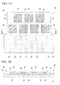
- Conductive circuits 32 that are formed in parallel on a surface 31a of a substrate 31 that constitutes a wiring substrate 30 are covered by an insulating layer 33. Opening portions 34 that expose the respective conductive circuits 32 are formed in a staggered arrangement.
- An electrode layer 35 that consists of a conductive member is formed on the conductive circuit 32 that is exposed from the opening portion 34. This electrode layer 35 extends so as to also cover a portion of the insulating layer 33.
- the electrode layers 35 have a staggered arrangement and are formed by being mutually shifted, even if the wiring interval of the conductive circuits 32 is further narrowed, since there is no interference between the mutually adjacent electrode layers 35, it is possible to achieve further fine pitching of the conductive circuits 32 in a fitting portion 36 of the wiring substrate 30, and even if a shift in the fitting position with the connector occurs in the wiring width direction, it is possible to reliably obtain an electrical connection by preventing conduction failures.
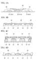
- FIG. 4A is a cross-sectional view that shows another embodiment of the wiring substrate of the present invention.
- This embodiment shows the wiring substrate such that the positions of adjacent electrodes 42 are arranged by being shifted.
- a conductive circuit 41 (41a) at the portion in which the electrode 42 is formed has a constitution in which its surface is covered with the electrode 42 without being covered by an insulating layer 43 between the adjacent conductive circuits 41 (41b) that are covered by the insulating layer 43.
- this kind of constitution even if a shift in the fitting position with the connector occurs in the wiring width direction, it is possible to reliably obtain an electrical connection by preventing conduction failures. Note that as shown in FIG.
- a structure is also possible in which the opening portions are arranged in an approximate line without being arranged in a staggered shape.
- a structure is also possible in which electrodes 52 are formed so as to overhang to the right and left on each conductive circuit 51, and insulating layers 53 are formed so as to completely bury the circuit space between the conductive circuits 51.
- Example 1 of the present invention a wiring substrate was prepared with a constitution of exposed surfaces of mutually adjacent conductive circuits forming a staggered arrangement, with the insulating layer extended for the conductive circuits of one side and an electrode layer not being provided as shown in FIG. 6 . Also, two levels of the wiring interval D were made by changing the wiring width W, and the superiority in the case of the interval being narrowed was compared. As the comparative example, as shown in FIG.
- a wiring substrate was prepared in which exposed surfaces of mutually adjacent conductive circuits form a staggered arrangement and the entire end portions of the conductive circuits are exposed without forming an insulating layer on the fitting portion and not providing an electrode layer.
- the wiring interval D of the conductive circuits is 50 to 70 ⁇ m serves as Comparative Example 1
- one with a wiring interval of 100 ⁇ m serves as Comparative Example 2.
- a silver paste was used for the conductive layer on all of the Example 1, Comparative Example 1, and Comparative Example 2.
- As the silver paste XA3060 (product name, manufactured by Fujikura Kasei) was used.
- each portion of the conductive circuit in FIGS. 5 to 7 is as given below.
- FIG. 5 50 ⁇ 70 (0/10) (0/10) Silver Paste - Comparative Example 2
- FIG. 5 100 (7/10) (0/10) Same - Example 1
- FIG. 6 50 ⁇ 70 (10/10) (5/10) Same - Example 2
- FIG. 7 50 ⁇ 70 (10/10) (7/10) Same Silver Paste Example 3
- FIG. 7 50 ⁇ 70 (10/10) (9/10) Same Copper Paste Example 4
- FIG. 7 50 ⁇ 70 (10/10) (10/10) Same Ni Paste Example 5
- the fitting portion with the connector if the insulating layer is arranged between adjacent conductive circuits and the electrode layer is formed on the exposed conductive circuits as in this constitution, since is possible to sufficiently maintain the fitting with the connector and it is possible to suppress defects between adjacent conductive circuits, it is possible to form a fitting portion with a fine-pitched structure.
- wiring substrates were prepared that cover all the conductive circuits with an insulating layer and form opening portions in the insulating layer so that exposed surfaces of mutually adjacent conductive circuits form a staggered arrangement and provide the electrode layer on the exposed conductive circuits.
- an Example 2 that makes the material of the conductive layer silver paste (XA3060 (product name, manufactured by Fujikura Kasei)), and uses silver paste (XA3060 (product name, manufactured by FUJIKURA KASEI CO., LTD.)) also for the electrode layer, an Example 3 that uses copper paste (NF2000 (product name: Tatsuta System Electronics)), an Example 4 that uses Ni paste (Namix), and an Example 5 that uses Au-plated Ni paste are prepared.
- Au-plated Ni paste is made into a paste by using conductive particulates 85 that consist of a thin gold plate around an Ni particulate, a phenol epoxy resin 15, and a carbitol acetate solution.
- the formation dimensions of each portion in FIG. 7 are the same as in paragraph [0022]. Note that, in FIG. 7 , the illustration of the electrode layer is omitted in order to simplify comprehension of the dimensions of the opening portion.
Landscapes
- Engineering & Computer Science (AREA)
- Microelectronics & Electronic Packaging (AREA)
- Manufacturing & Machinery (AREA)
- Printing Elements For Providing Electric Connections Between Printed Circuits (AREA)
- Coupling Device And Connection With Printed Circuit (AREA)
- Parts Printed On Printed Circuit Boards (AREA)
Abstract
Description
- The present invention relates to a wiring substrate that is provided with a fitting portion for connection with a connector.
- A fitting portion for connecting a wiring substrate with a connector of another device conventionally has a structure in which a portion of conductive circuits that are formed on one surface of the substrate are exposed, with contact points of the connector side brought into contact with the exposed portions of the conductive circuits to be electrically connected, as shown in
FIG. 8A and FIG. 8B . In the fitting portion of this wiring substrate, in addition to reducing the diameter of the connection by miniaturization and thinning of the device, fine pitching of the conductive circuits is increasingly progressing. - However, there is a risk of easily causing electrical faults between adjacent conductive circuits by narrowing the wiring interval of the conductive circuits and fine pitching of the conductive circuits.
- Also, when the size of the conductive circuit at the portion that makes contact with the contact point of the connector is reduced and fine pitching of the conductive circuits is performed, then as shown in
FIG. 9 if a shift occurs in which theconnectors 86 move slightly in the wiring width direction W, the disadvantage easily occurs in which eachconnector 86 separates from the exposedsurface 83a of theconductive circuit 83, and so an electrical connection cannot be made between theconnectors 86 and theconductive circuits 83.
Also, in the case of the constitution ofFIG. 8A , there is known one that is provided with a coveringlayer 105 that is formed by coating a migration resistant resin (a paste material) on the outer periphery of a printedcircuit portion 102 that is formed on the upper surface of awiring substrate 101 in order to suppress migration resistance, as shown inFIG. 10 . In the case of this substrate structure, when fine pitching is performed, due to the accuracy of the printing, there is a risk of the side surface portion of the printed circuit being exposed because a sufficient covering layer cannot be formed. When the printing circuit is exposed, migration readily occurs, which becomes an impediment to fine pitching. - Patent Document 1: Japanese Unexamined Patent Application, First Publication No.
H06-132057 - The present invention was achieved in view of the above circumstances, and has as its object to provide a wiring substrate that is provided with a fitting portion that can prevent electrical faults between conductive circuits and is compatible with a fine pitch structure without impairing the fitting with a connector.
- The wiring substrate according to one aspect of the present invention is a wiring substrate that is provided with a fitting portion for connection with a connector, characterized in that the wiring substrate includes a substrate; a plurality of conductive circuits that are arranged in parallel on one surface of the substrate; an insulating layer that covers the conductive circuits; opening portions that are provided in the insulating layer at the fitting portion and expose at least a portion of the conductive circuits; and a plurality of electrodes that are disposed on the exposed conductive circuits through the opening portion and consist of a conductive member; at least one among the electrodes being disposed so as to cover the exposed portion of the conductive circuit and a portion of the insulating layer in the wiring width direction of the conductive circuit.
It is preferable that the electrode contains a member that has migration resistance.
Also, it is preferable that each electrode covers the entirety of a corresponding opening portion.
Further, it is preferable that the surface of the insulating layer portion that is partially covered by each electrode has a tapered shape.
Still further, it is preferable that the upper surface of the electrodes is the same height as or higher than the upper surface of the insulating layer.
Even still further, it is preferable that the electrodes are disposed in an approximate line when the substrate is viewed in plane view.
Separately, it is preferable that the electrodes are disposed in a staggered shape when the substrate is viewed in plane view. - According to the wiring substrate of the present invention, it is possible to sufficiently maintain a fitting with a connector. Also, since an insulating layer is provided between conductive circuits, it is possible to suppress electrical faults between adjacent conductive circuits and possible to form a fitting portion with a fine pitching structure.
-
-
FIG. 1 is a perspective view that shows the wiring substrate of one embodiment of the present invention. -
FIG. 2A is a sectional view alongline 2A-2A of the wiring substrate shown inFIG. 1 . -
FIG. 2B is a traverse sectional view of the wiring substrate. -
FIG. 3A is a plane view of the wiring substrate of one embodiment of the present invention. -
FIG. 3B is a sectional view alongline 3B-3B of the wiring substrate shown inFIG. 3A . -
FIG. 4A is a sectional view that shows another example of the wiring substrate according to the present invention. -
FIG. 4B is a sectional view that shows a separate example of the wiring substrate according to the present invention. -
FIG. 4C is a sectional view that shows yet another example of the wiring substrate according to the present invention. -
FIG. 4D is a sectional view that shows still yet another example of the wiring substrate according to the present invention. -
FIG. 5 is a plan view that shows the wiring substrate of the comparative example. -
FIG. 6 is a plan view that shows the wiring substrate of the embodiment of the present invention. -
FIG. 7 is a plan view that shows the wiring substrate of the embodiment of the present invention. -
FIG. 8A is a main portion plan view that shows an example of a conventional wiring substrate. -
FIG. 8B is a main portion plan view that shows another example of a conventional wiring substrate. -
FIG. 9 is a sectional view that shows a separate example of a conventional wiring substrate. -
FIG. 10 is a sectional view that shows yet another example of a conventional wiring substrate. -
- 10 wiring substrate
- 11 substrate
- 12 conductive circuit
- 13 insulating layer
- 14 fitting portion
- 15 electrode layer
- 18 opening portion
- Hereinbelow, a plurality of embodiments of the wiring substrate according to the present invention shall be described with reference to the drawings. Note that the present invention is not limited to these embodiments.
FIG. 1 is a perspective view of the fitting portion vicinity in the wiring substrate of one embodiment of the present invention.FIG. 2A is a sectional view along line A-A ofFIG. 1 . Awiring substrate 10 of the present embodiment is provided with asubstrate 11, aconductive circuit 12 that is formed on onesurface 11 a of thissubstrate 11, and an insulatinglayer 13 that covers thisconductive circuit 12. In thiswiring substrate 10, for example, afitting portion 14 is formed that fits with aconnector 21 such as another device. - In the
connector portion 14 of thiswiring substrate 10, an openingportion 18 is formed that exposes a portion of theconductive circuit 12 so as to partition an individualconductive circuit 12 to the insulatinglayer 13. In thisopening portion 18, a portion of theconductive circuit 12 is exposed from the insulatinglayer 13 as an exposedsurface 12a. - Moreover, on the exposed
surface 12a of thisconductive circuit 12, anelectrode layer 15 that consists of a conductive member is formed. Thiselectrode layer 15 makes contact with theconductive circuit 12 at its lower surface, while the upper surface thereof is extended so as to also cover a portion of the insulatinglayer 13 in the wiring width direction W of theconductive circuit 12. Thereby, an electrode width L2 in the wiring width direction W of the upper surface of theelectrode layer 15 is greater than a wiring width L1 of theconductive circuit 12. - When fine pitching is performed by extreme narrowing of the wiring width (the size of the portions that make contact with the connectors) of the conductive circuits, with merely a slight shift of the fitting location with the connectors, the connectors end up riding onto the insulating layer, leading to a conduction failure as electrical contact with the conductive circuits cannot be made. A need therefore arises to increase the fitting accuracy of the fitting portion with respect to the connectors by fine pitching, which may increase manufacturing cost.
- However, by adopting the constitution of the present invention as described above, even if the wiring width L1 of the
conductive circuit 12 narrows, it is possible to sufficiently ensure the contact points with the connectors by theelectrode layer 15 consisting of a conductive member spreading on theconductive circuit 12 so as to also cover a portion of the insulatinglayer 13. Therefore, even if the fitting with theconnector 21 shifts slightly in the wiring width direction W, it is possible to sufficiently ensure conduction between theconnector 21 and theconductive circuit 12 via thiselectrode layer 15. Thereby, it is possible to sufficiently ensure the insulation performance between adjacentconductive circuits 12 and reliably prevent conduction failures due to shifting of the fitting location between theconnector 21 and theconductive circuit 12. For that reason, it is possible to perform fine pitching of theconductive circuits 12 of thefitting portion 14 on thewiring substrate 10. Also, as shown inFIG. 2B , a plurality ofconductive circuits 23 are opened so as to be individually exposed on asubstrate 24, and an insulatinglayer 22 is formed between the opening portions of the mutually adjacentconductive circuits conductive circuits 23 is reduced by fine pitching, it is possible to eliminate electrical malfunctions in theconductive circuits - Note the
electrode layer 15 may have a constitution that covers theentire opening portion 18 or only a portion thereof. Also, asurface 13a of the insulatinglayer 13 at the portion that is partially covered by theelectrode layer 15 is preferably formed in a tapered shape. If thesurface 13a of the insulatinglayer 13 is formed in a tapered shaped, when theelectrode layer 15 is applied using a conductive paste, it is possible to achieve a flattening of the upper surface of theelectrode layer 15 by the conductive paste flowing between adjacent insulatinglayers 13, and so improve the connectability with the connector. - Also, it is preferable that the upper surface of the
electrode layer 15 is formed so as to be the same height as the upper surface of the insulatinglayer 13 or higher. Thereby, during attachment and removal of the connector to/from the fitting portion, when the connector hits the upper surface of the insulatinglayer 13, it is possible to prevent damage to the insulatinglayer 13 due to scraping of the insulatinglayer 13, which is formed with a soft material such as resin or the like, and the loss of insulation performance. Also, if the height of the upper surface of theelectrode layer 15 is made to be the same height as the upper surface of the insulatinglayer 13, the fitting with the connector is improved, and so it is possible to more reliably achieve conduction with the connector. Also, if the height of the upper surface of theelectrode layer 15 is made to be higher than the height of the upper surface of the insulatinglayer 13, during insertion/extraction of theconnector 21 into/from thefitting portion 14, the connector does not hit the soft insulatinglayer 13, which proves useful for maintaining the insulation performance by protecting the insulatinglayer 13. - It is preferable that the
substrate 10 be an electrically insulating substrate made of resin. This kind ofsubstrate 10 constitutes a connection wiring substrate with the connector that is connected to the flexible substrate.
It is preferable that theconductive circuit 12 is a conductor that includes Ag or Cu from the point of low material cost and low resistance. It is preferable that thisconductive circuit 12 be formed by applying a conductive paste that includes for example Ag or Cu on thesubstrate 10 in a predetermined pattern. When applying this conductive paste, a method such as screen printing or ink jet printing may be used from the standpoint of lowering cost. It is preferable that the insulatinglayer 13 be formed from an insulating resin, such as polyester resin, polyurethane resin, phenol resin, epoxy resin and the like.
It is preferable that this resin with an insulating performance is printed by a method such as screen printing as an insulating paste that includes a solvent, but is not limited thereto. - It is preferable that the
electrode layer 15 uses a material with a conductivity that is as low as possible. If constituted from such a member, even if the distance between theconductive circuit 12 and theconnector 21 separates due to a shift of theconnector 21, it is possible to enable a low electrical resistance via theelectrode layer 15.
As a method of forming theelectrode layer 15, it is possible to use both a vacuum process such as the sputtering method or vapor deposition method and a wet type process such as a screen printing method or ink jet printing method.
Concerning the materials that can be used for theelectrode layer 15, in relation to formation with the vacuum process, it is possible to use all metal materials. However, in the case of coating with a method such as a printing method, it is limited to a low-resistance material, such as a silver paste or gold paste. In relation to a low cost and large surface area, the latter printing method is advantageous. - Also, as the constituent members of the
electrode layer 15, it is preferable to use a migration resistant material that is effective in suppressing migration. As a migration resistant material, it is preferable to use a material that contains little or no copper or silver components. Moreover, a material that is capable of being printed is preferable in order to lower costs, including for example, a conductive paste that consists of Ni particulates and a resin component, a conductive paste that contains gold-plated particulates and a resin component, and a carbon paste or soldering paste. By constituting theelectrode layer 15 with such a migration resistant material, it is possible to suppress the occurrence of migration even when using a material such as Ag and Cu that has excellent conductivity and in which migration occurs easily as theconductive circuit 12. -
FIG. 3A and FIG. 3B are drawings that show the first embodiment of the wiring substrate of the present invention. In this embodiment, by shifting the opening portions of mutually adjacent conductive circuits to make a staggered arrangement, fine pitching of the conductive circuits is achieved in the fitting portion.Conductive circuits 32 that are formed in parallel on asurface 31a of asubstrate 31 that constitutes awiring substrate 30 are covered by an insulatinglayer 33. Openingportions 34 that expose the respectiveconductive circuits 32 are formed in a staggered arrangement. Anelectrode layer 35 that consists of a conductive member is formed on theconductive circuit 32 that is exposed from the openingportion 34. Thiselectrode layer 35 extends so as to also cover a portion of the insulatinglayer 33. - According to this constitution, since the electrode layers 35 have a staggered arrangement and are formed by being mutually shifted, even if the wiring interval of the
conductive circuits 32 is further narrowed, since there is no interference between the mutually adjacent electrode layers 35, it is possible to achieve further fine pitching of theconductive circuits 32 in afitting portion 36 of thewiring substrate 30, and even if a shift in the fitting position with the connector occurs in the wiring width direction, it is possible to reliably obtain an electrical connection by preventing conduction failures. -
FIG. 4A is a cross-sectional view that shows another embodiment of the wiring substrate of the present invention. This embodiment shows the wiring substrate such that the positions ofadjacent electrodes 42 are arranged by being shifted. A conductive circuit 41 (41a) at the portion in which theelectrode 42 is formed has a constitution in which its surface is covered with theelectrode 42 without being covered by an insulatinglayer 43 between the adjacent conductive circuits 41 (41b) that are covered by the insulatinglayer 43. In this kind of constitution, even if a shift in the fitting position with the connector occurs in the wiring width direction, it is possible to reliably obtain an electrical connection by preventing conduction failures.
Note that as shown inFIG. 4B , a structure is also possible in which the opening portions are arranged in an approximate line without being arranged in a staggered shape.
Also, as shown inFIG. 4C and FIG. 4D , a structure is also possible in whichelectrodes 52 are formed so as to overhang to the right and left on eachconductive circuit 51, and insulatinglayers 53 are formed so as to completely bury the circuit space between theconductive circuits 51. - The effect relating to the insulating performance by fine pitching of the wiring substrate was investigated. In the investigation, as Example 1 of the present invention, a wiring substrate was prepared with a constitution of exposed surfaces of mutually adjacent conductive circuits forming a staggered arrangement, with the insulating layer extended for the conductive circuits of one side and an electrode layer not being provided as shown in
FIG. 6 . Also, two levels of the wiring interval D were made by changing the wiring width W, and the superiority in the case of the interval being narrowed was compared.
As the comparative example, as shown inFIG. 5 , a wiring substrate was prepared in which exposed surfaces of mutually adjacent conductive circuits form a staggered arrangement and the entire end portions of the conductive circuits are exposed without forming an insulating layer on the fitting portion and not providing an electrode layer. Therein, one in which the wiring interval D of the conductive circuits is 50 to 70 µm serves as Comparative Example 1, and one with a wiring interval of 100 µm serves as Comparative Example 2. Also, a silver paste was used for the conductive layer on all of the Example 1, Comparative Example 1, and Comparative Example 2. As the silver paste, XA3060 (product name, manufactured by Fujikura Kasei) was used. - The formation dimensions of each portion of the conductive circuit in
FIGS. 5 to 7 are as given below. - S1 = 300 µm
- S2 (wiring interval D) = 50 to 70 µm (Examples 1 to 5, Comparative Example 1), 100 µm (Comparative Example 2)
- S3 = 300 µm
- S4 (wiring width W) = S1 -
S2 x 2 µm - wiring thickness H = 200 µm
- Then, the wiring substrate of Example 1, and the respective wiring substrates of Comparative Example 1 and Comparative Example 2 were impressed with a 5V voltage with the polarity shown in each drawing in an environment of a temperature of 60°C and humidity of 95%. Then, after 240 hours and 1,000 hours, among 10 samples of each, those in which adjacent wiring substrates electrically shorted were inspected. The investigation results are presented in Table 1.
-
[Table 1] Sample Corresponding Drawing Smallest Wiring Interval Evaluation (Non-defective No./Examined No.) Material (Electrode Layer 12) Material (Electrode Layer 15) After 240 Hours After 1,000 Hours Comparative Example 1 FIG. 5 50∼70 (0/10) (0/10) Silver Paste - Comparative Example 2 FIG. 5 100 (7/10) (0/10) Same - Example 1 FIG. 6 50∼70 (10/10) (5/10) Same - Example 2 FIG. 7 50∼70 (10/10) (7/10) Same Silver Paste Example 3 FIG. 7 50∼70 (10/10) (9/10) Same Copper Paste Example 4 FIG. 7 50∼70 (10/10) (10/10) Same Ni Paste Example 5 FIG. 7 50∼70 (10/10) (10/10) Same Au-plated Ni Paste - As is evident from the inspection result shown in Table 1, in the Comparative Example 2 that sets the wiring interval at 100 µm, at the point at which 240 hours have elapsed, three of the 10 samples short-circuited, and after the passage of 1,000 hours, all 10 short-circuited. Also, in the Comparative Example 1 with a wiring interval of 50 to 70 µm, after the passage of 240 hours, all 10 short-circuited.
In the wiring substrate of Example 1, even with a wiring interval of 50 to 70 µm, at the point when 240 hours have elapsed, the insulating property is maintained with none of the 10 samples short-circuiting. Also, even after 1,000 hours have elapsed, only five have short-circuited, and at least half have maintained their insulating property. Therefore, in the fitting portion with the connector, if the insulating layer is arranged between adjacent conductive circuits and the electrode layer is formed on the exposed conductive circuits as in this constitution, since is possible to sufficiently maintain the fitting with the connector and it is possible to suppress defects between adjacent conductive circuits, it is possible to form a fitting portion with a fine-pitched structure. - Also, as separate examples of the present invention, as show in
FIG. 7 , wiring substrates were prepared that cover all the conductive circuits with an insulating layer and form opening portions in the insulating layer so that exposed surfaces of mutually adjacent conductive circuits form a staggered arrangement and provide the electrode layer on the exposed conductive circuits. Then, an Example 2 that makes the material of the conductive layer silver paste (XA3060 (product name, manufactured by Fujikura Kasei)), and uses silver paste (XA3060 (product name, manufactured by FUJIKURA KASEI CO., LTD.)) also for the electrode layer, an Example 3 that uses copper paste (NF2000 (product name: Tatsuta System Electronics)), an Example 4 that uses Ni paste (Namix), and an Example 5 that uses Au-plated Ni paste are prepared. Among these, Au-plated Ni paste is made into a paste by using conductive particulates 85 that consist of a thin gold plate around an Ni particulate, aphenol epoxy resin 15, and a carbitol acetate solution. Also, the formation dimensions of each portion inFIG. 7 are the same as in paragraph [0022]. Note that, inFIG. 7 , the illustration of the electrode layer is omitted in order to simplify comprehension of the dimensions of the opening portion. - For these Examples 2 to 5, according to the investigation results shown in Table 1, in the case of forming the electrode layer with any material, the insulating performance was maintained without short circuiting in the 10 samples after the passage of 240 hours.
Also, even after the passage of 1,000 hours, at the most only three of 10 samples short-circuited. Also, for those that used Ni paste or Au-plated Ni paste that have excellent migration resistance for the electrode layer, none of the 10 samples short-circuited.
According to the wiring substrate of the present invention, even when the interval of the conductive circuits narrows, the insulating performance is sufficient, so fine pitching of the conductive circuits is possible. It was confirmed that the insulating performance is significantly improved. Note that the effect of the present invention is not limited to the wiring substrate of the shape shown inFIG. 6 andFIG. 7 .
Claims (7)
- A wiring substrate that is provided with a fitting portion for connection with a connector, characterized in that the wiring substrate comprises:a substrate;a plurality of conductive circuits that are arranged in parallel on one surface of the substrate;an insulating layer that covers the conductive circuits;opening portions that are provided in the insulating layer at the fitting portion and expose at least a portion of the conductive circuits; anda plurality of electrodes that are disposed on the exposed conductive circuits through the opening portion and consist of a conductive member;at least one among the electrodes being disposed so as to cover the exposed portion of the conductive circuit and a portion of the insulating layer in the wiring width direction of the conductive circuit.
- The wiring substrate of claim 1, characterized by the electrode containing a member that has migration resistance.
- The wiring substrate of claim 1, characterized by each electrode covering the entirety of a corresponding opening portion.
- The wiring substrate of claim 1, characterized by the surface of the insulating layer portion that is partially covered by each electrode having a tapered shape.
- The wiring substrate of claim 1, characterized by the upper surface of the electrodes being the same height as or higher than the upper surface of the insulating layer.
- The wiring substrate of claim 1, characterized by the electrodes being disposed in an approximate line when the substrate is viewed in plane view.
- The wiring substrate of claim 1, characterized by the electrodes being disposed in a staggered shape when the substrate is viewed in plane view.
Applications Claiming Priority (2)
| Application Number | Priority Date | Filing Date | Title |
|---|---|---|---|
| JP2006148722 | 2006-05-29 | ||
| PCT/JP2007/060844 WO2007139076A1 (en) | 2006-05-29 | 2007-05-28 | Wiring board |
Publications (2)
| Publication Number | Publication Date |
|---|---|
| EP2023697A1 true EP2023697A1 (en) | 2009-02-11 |
| EP2023697A4 EP2023697A4 (en) | 2012-11-14 |
Family
ID=38778596
Family Applications (1)
| Application Number | Title | Priority Date | Filing Date |
|---|---|---|---|
| EP07744278A Withdrawn EP2023697A4 (en) | 2006-05-29 | 2007-05-28 | Wiring board |
Country Status (7)
| Country | Link |
|---|---|
| US (1) | US8222536B2 (en) |
| EP (1) | EP2023697A4 (en) |
| JP (1) | JP4979598B2 (en) |
| KR (1) | KR101031620B1 (en) |
| CN (1) | CN101455130B (en) |
| TW (1) | TWI342178B (en) |
| WO (1) | WO2007139076A1 (en) |
Cited By (1)
| Publication number | Priority date | Publication date | Assignee | Title |
|---|---|---|---|---|
| EP2219426A1 (en) * | 2009-02-02 | 2010-08-18 | Beckhoff Automation GmbH | Method for manufacturing contacts |
Families Citing this family (7)
| Publication number | Priority date | Publication date | Assignee | Title |
|---|---|---|---|---|
| JP2010021371A (en) * | 2008-07-10 | 2010-01-28 | Fujitsu Ltd | Printed wiring board, wiring manufacturing method, and conductive paste |
| JP2010192802A (en) | 2009-02-20 | 2010-09-02 | Sony Corp | Mounting board and display apparatus |
| JP5612443B2 (en) * | 2010-11-08 | 2014-10-22 | 株式会社フジクラ | Printed wiring board and printed wiring board manufacturing method |
| TWI393495B (en) * | 2010-12-03 | 2013-04-11 | Adv Flexible Circuits Co Ltd | Electrical impedance precision control of signal transmission line for circuit board |
| TWI537664B (en) | 2014-08-22 | 2016-06-11 | 元太科技工業股份有限公司 | Bottom electrode substrate for segment-type electro-phoretic display and method for manufacturing thereof |
| JP2018157128A (en) * | 2017-03-21 | 2018-10-04 | 株式会社東海理化電機製作所 | Circuit board |
| CN114222439A (en) * | 2022-01-20 | 2022-03-22 | 江苏煊葳光电科技有限公司 | A kind of silver-nickel composite circuit substrate and preparation method thereof |
Family Cites Families (12)
| Publication number | Priority date | Publication date | Assignee | Title |
|---|---|---|---|---|
| JPH03173007A (en) * | 1989-12-01 | 1991-07-26 | Kao Corp | Conductive paste and conductive film |
| JPH06132057A (en) | 1992-10-14 | 1994-05-13 | Nippondenso Co Ltd | Structure for connection between flexible printed wiring board and circuit board |
| JP3057156B2 (en) * | 1998-10-08 | 2000-06-26 | 日本特殊陶業株式会社 | Wiring board and its manufacturing method |
| JP2001077494A (en) | 1999-09-08 | 2001-03-23 | Matsushita Electric Ind Co Ltd | Printed wiring board |
| TW429492B (en) * | 1999-10-21 | 2001-04-11 | Siliconware Precision Industries Co Ltd | Ball grid array package and its fabricating method |
| JP2003216055A (en) | 2002-01-21 | 2003-07-30 | Mitsubishi Electric Corp | Interposer, method of manufacturing the same, and flat panel display with interposer |
| JP3819806B2 (en) * | 2002-05-17 | 2006-09-13 | 富士通株式会社 | Electronic component with bump electrode and manufacturing method thereof |
| EP1387604A1 (en) * | 2002-07-31 | 2004-02-04 | United Test Center Inc. | Bonding pads of printed circuit board capable of holding solder balls securely |
| JP2004079811A (en) * | 2002-08-19 | 2004-03-11 | Hokuriku Electric Ind Co Ltd | Chip electronics component and its fabricating process |
| JP4054633B2 (en) * | 2002-08-20 | 2008-02-27 | シャープ株式会社 | Active matrix substrate, method for manufacturing the same, and liquid crystal display device including the same |
| CN1697318A (en) * | 2004-04-13 | 2005-11-16 | 松下电器产业株式会社 | Electronic component having side electrodes, manufacturing method thereof, and device using the electronic component |
| US20060049265A1 (en) * | 2004-09-07 | 2006-03-09 | Richip Incorporated | Interface for a removable electronic device |
-
2007
- 2007-05-28 WO PCT/JP2007/060844 patent/WO2007139076A1/en not_active Ceased
- 2007-05-28 JP JP2007558252A patent/JP4979598B2/en active Active
- 2007-05-28 EP EP07744278A patent/EP2023697A4/en not_active Withdrawn
- 2007-05-28 KR KR1020087029091A patent/KR101031620B1/en not_active Expired - Fee Related
- 2007-05-28 CN CN2007800192531A patent/CN101455130B/en not_active Expired - Fee Related
- 2007-05-28 TW TW096118945A patent/TWI342178B/en not_active IP Right Cessation
-
2008
- 2008-11-26 US US12/324,516 patent/US8222536B2/en not_active Expired - Fee Related
Cited By (1)
| Publication number | Priority date | Publication date | Assignee | Title |
|---|---|---|---|---|
| EP2219426A1 (en) * | 2009-02-02 | 2010-08-18 | Beckhoff Automation GmbH | Method for manufacturing contacts |
Also Published As
| Publication number | Publication date |
|---|---|
| KR20090014360A (en) | 2009-02-10 |
| CN101455130A (en) | 2009-06-10 |
| JPWO2007139076A1 (en) | 2009-10-08 |
| WO2007139076A1 (en) | 2007-12-06 |
| US20090139748A1 (en) | 2009-06-04 |
| EP2023697A4 (en) | 2012-11-14 |
| TWI342178B (en) | 2011-05-11 |
| US8222536B2 (en) | 2012-07-17 |
| KR101031620B1 (en) | 2011-05-02 |
| JP4979598B2 (en) | 2012-07-18 |
| TW200810656A (en) | 2008-02-16 |
| CN101455130B (en) | 2012-05-09 |
Similar Documents
| Publication | Publication Date | Title |
|---|---|---|
| US8222536B2 (en) | Wiring substrate | |
| EP2234466B1 (en) | Mounting board and method of producing the same | |
| JP4614278B2 (en) | Electronic circuit unit and manufacturing method thereof | |
| US20130264107A1 (en) | Circuit board and wire assembly | |
| US7881040B2 (en) | Feedthrough capacitor mounted structure | |
| CN101098586A (en) | Wiring circuit board | |
| JP4133786B2 (en) | Printed circuit board | |
| CN1106023C (en) | Feedthrough thin-film capacitor and interfering-signal-removing assembly fitted with same | |
| CN101160016A (en) | Wiring circuit board | |
| US8031480B2 (en) | Structure for mounting feedthrough capacitors | |
| WO2019020220A1 (en) | SENSOR FOR DETECTING A SPATIAL TEMPERATURE PROFILE AND METHOD FOR PRODUCING A SENSOR UNIT | |
| US6345989B1 (en) | Circuit board side interconnect | |
| DE10301741A1 (en) | Printed circuit board comprising a conductive ink layer forming conductive paths between vias and an enhanced ink layer with a lower conductivity and higher moisture resistance than the conductive ink layer | |
| US20080296051A1 (en) | Printed circuit board | |
| JPH05335714A (en) | Multilayer flexible installation substrate | |
| JP2009099837A5 (en) | ||
| CN110176354B (en) | Multilayer capacitor | |
| JP4102675B2 (en) | Flexible wiring board and liquid crystal display device | |
| JPH08242053A (en) | Printed wiring board | |
| DE102007014579B4 (en) | microphone | |
| CN2904300Y (en) | Improvement of chip module | |
| US20250358929A1 (en) | Connection circuit and method of manufacturing connection circuit | |
| JPH066006A (en) | Component terminal connection structure | |
| KR101321499B1 (en) | Printed circuit board and flat panel display apparatus comprising the same | |
| JP2007088243A (en) | Flexible printed circuit board |
Legal Events
| Date | Code | Title | Description |
|---|---|---|---|
| PUAI | Public reference made under article 153(3) epc to a published international application that has entered the european phase |
Free format text: ORIGINAL CODE: 0009012 |
|
| 17P | Request for examination filed |
Effective date: 20081127 |
|
| AK | Designated contracting states |
Kind code of ref document: A1 Designated state(s): AT BE BG CH CY CZ DE DK EE ES FI FR GB GR HU IE IS IT LI LT LU LV MC MT NL PL PT RO SE SI SK TR |
|
| AX | Request for extension of the european patent |
Extension state: AL BA HR MK RS |
|
| RIN1 | Information on inventor provided before grant (corrected) |
Inventor name: ONO, AKINOBUFUJIKURA LTD. Inventor name: HIRATA, SHUZOFUJIKURA LTD. |
|
| DAX | Request for extension of the european patent (deleted) | ||
| RBV | Designated contracting states (corrected) |
Designated state(s): DE FI FR GB SE |
|
| A4 | Supplementary search report drawn up and despatched |
Effective date: 20121016 |
|
| RIC1 | Information provided on ipc code assigned before grant |
Ipc: H05K 1/11 20060101AFI20121010BHEP |
|
| 17Q | First examination report despatched |
Effective date: 20130701 |
|
| STAA | Information on the status of an ep patent application or granted ep patent |
Free format text: STATUS: THE APPLICATION IS DEEMED TO BE WITHDRAWN |
|
| 18D | Application deemed to be withdrawn |
Effective date: 20140709 |