EP2019490A1 - Segmented circuitry - Google Patents
Segmented circuitry Download PDFInfo
- Publication number
- EP2019490A1 EP2019490A1 EP07113376A EP07113376A EP2019490A1 EP 2019490 A1 EP2019490 A1 EP 2019490A1 EP 07113376 A EP07113376 A EP 07113376A EP 07113376 A EP07113376 A EP 07113376A EP 2019490 A1 EP2019490 A1 EP 2019490A1
- Authority
- EP
- European Patent Office
- Prior art keywords
- segment
- segments
- circuitry
- node
- segmented
- Prior art date
- Legal status (The legal status is an assumption and is not a legal conclusion. Google has not performed a legal analysis and makes no representation as to the accuracy of the status listed.)
- Granted
Links
- 239000003990 capacitor Substances 0.000 claims description 15
- 230000003071 parasitic effect Effects 0.000 claims description 15
- 238000000034 method Methods 0.000 description 10
- 230000001934 delay Effects 0.000 description 6
- 230000000694 effects Effects 0.000 description 5
- 101100115778 Caenorhabditis elegans dac-1 gene Proteins 0.000 description 4
- 229910021420 polycrystalline silicon Inorganic materials 0.000 description 4
- 229920005591 polysilicon Polymers 0.000 description 4
- 238000004458 analytical method Methods 0.000 description 3
- 238000004519 manufacturing process Methods 0.000 description 3
- 229920005994 diacetyl cellulose Polymers 0.000 description 2
- 238000005516 engineering process Methods 0.000 description 2
- 230000036039 immunity Effects 0.000 description 2
- 239000002184 metal Substances 0.000 description 2
- 230000011664 signaling Effects 0.000 description 2
- 230000000295 complement effect Effects 0.000 description 1
- 230000001419 dependent effect Effects 0.000 description 1
- 238000010586 diagram Methods 0.000 description 1
- 230000002452 interceptive effect Effects 0.000 description 1
- 230000001902 propagating effect Effects 0.000 description 1
- 229920006395 saturated elastomer Polymers 0.000 description 1
- 230000011218 segmentation Effects 0.000 description 1
Images


Classifications
-
- H—ELECTRICITY
- H03—ELECTRONIC CIRCUITRY
- H03M—CODING; DECODING; CODE CONVERSION IN GENERAL
- H03M1/00—Analogue/digital conversion; Digital/analogue conversion
- H03M1/66—Digital/analogue converters
- H03M1/74—Simultaneous conversion
- H03M1/78—Simultaneous conversion using ladder network
-
- H—ELECTRICITY
- H03—ELECTRONIC CIRCUITRY
- H03M—CODING; DECODING; CODE CONVERSION IN GENERAL
- H03M1/00—Analogue/digital conversion; Digital/analogue conversion
- H03M1/66—Digital/analogue converters
- H03M1/68—Digital/analogue converters with conversions of different sensitivity, i.e. one conversion relating to the more significant digital bits and another conversion to the less significant bits
- H03M1/682—Digital/analogue converters with conversions of different sensitivity, i.e. one conversion relating to the more significant digital bits and another conversion to the less significant bits both converters being of the unary decoded type
-
- H—ELECTRICITY
- H03—ELECTRONIC CIRCUITRY
- H03M—CODING; DECODING; CODE CONVERSION IN GENERAL
- H03M1/00—Analogue/digital conversion; Digital/analogue conversion
- H03M1/66—Digital/analogue converters
- H03M1/74—Simultaneous conversion
- H03M1/742—Simultaneous conversion using current sources as quantisation value generators
- H03M1/747—Simultaneous conversion using current sources as quantisation value generators with equal currents which are switched by unary decoded digital signals
Abstract
Description
- The present invention relates to segmented circuitry, in particular to segmented mixed-signal circuitry, for example a segmented digital-to-analogue converter (DAC) or a segmented programmable current generator.
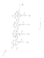
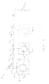
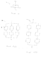
- One architecture which has been used to implement a DAC is a so-called R-2R ladder architecture. The basic building block of such an R-2R DAC is an R-2R ladder of the kind shown in
Figure 1 . InFigure 1 , aresistor ladder 1 comprises a series of nodes N1, N2, N3 and N4. Each node is connected to the next node by a divider resistor. These divider resistors are all identical to one another and have a resistance R. The first node N1 is connected to a reference node RN at which a reference voltage Vref is generated. The fourth node N4 is connected to a ground supply line via a terminating resistor which has a resistance of 2R. Each of the nodes N1 to N4 is also connected to the ground supply line by a load resistor which in this case has a resistance value of 2R. - Operation of the
resistor ladder 1 can be understood by considering the resistances looking into different parts of the ladder. A resistance R4R looking into the termination resistor at node N4 is simply 2R. A resistance R4L looking into node N4 from the left-hand-side is 2R in parallel with 2R, which is equivalent to a single resistance R. A resistance R3R looking into the divider resistor on the right-hand-side of node N3 is R in series with R4L, which is equivalent to asingle resistance 2R. A resistance R3L looking into the node N3 from the left-hand-side is 2R in parallel with R3R, which is equivalent to a single resistance R. If this analysis is continued all the way through to node N1, it is found that R1R=R2R=R3R=R4R=2R. Similarly, it is found that R1L=R2L=R3L=R4L=R. - It can be seen that a current I1 flowing between N1 and ground is equal to Vref/2R. Because R1R is equal to the resistance of the load resistor connected between N1 and ground, it follows that a current equal to I1 flows into node N2 from
N 1. At the node N2 this current is split into two equal parts, the first part of which is the current I2 flowing from N2 to ground and the second part of which is the current flowing from N2 into N3. The two parts are equal because R2R is equal to theresistance 2R of the load resistor between N2 and ground. It therefore follows that I2 = Vref/4R. The same is true at the nodes N3 and N4 so that I3 = Vref/8R and I4 = Vref/16R. - Accordingly, the
ladder 1 can achieve binary-weighted currents using relatively few components. Also, the load resistors can be constructed by using two of the divider resistors in series. This should enable a better matching to be achieved between the load resistors and the divider resistors. - One example of an R-2R DAC using such an R-2R ladder is shown in
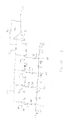
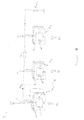
Figure 2 . In this case, the load resistors are connected between the nodes N1 to N4 and respective selection switches S1 to S4, instead of being connected to ground as inFigure 1 . Accordingly, depending upon the position of each selection switch S1 to S4, the load resistor is either connected to ground or to a connection line L1. The connection line L1 is also connected to an inverting input of anamplifier 3. As is known in the art, since theoperational amplifier 3 has a very high open loop gain, it acts to make the potential diference between its inputs tend to zero. Because the non-inverting input (+) is grounded, the inverting input (-) will assume a similar potential and can therefore be regarded as a "virtual ground". That is, it is maintained at substantially ground potential irrespective of an output Vout of the amplifier. Accordingly, respective potentials of the upper ends of the load resistors in the ladder remain at ground potential irrespective of the positions of the selection switches S1 to S4. This means that the ladder arrangement operates in the same way as inFigure 1 , and the currents which flow through the load resistors are binary weighted, i.e. I, I/2, I/4 and I/8, where I = Vref/2R. - The switches S1 to S4 in
Figure 2 correspond respectively to different data bits b1 to b4 of a binary input signal of the DAC. The setting of the switch is by the corresponding data bit. Thus, when b1 = 0, the selection switch S1 connects the load resistor for node N1 to ground. When b1 = 1, the selection switch S1 connects the load resistor for node N1 to the connection line L1. Accordingly, the current I flows from the connection line L1 to the node N1. A current Iin flowing into the connection line L1 is therefore changed by I depending on the setting of the switch S1. The same is true for each of the other selection switches S2 to S4. - For example, when all of the data bits b1 to b4 are 1 the selection switches S1 to S4 have the positions shown in
Figure 2 . In this case Iin becomes the sum of the currents flowing through the four load resistors of the ladder arrangement, i.e. I+I/2+I/4+I/8=15I/8. The output voltage Vout of the amplifier is Iin.RF, where RF is the resistance of afeedback resistor 4 connected between the non-inverting input of theamplifier 3 and the output thereof. It therefore follows that Vout=Vref.(RF/2R).[b1+b2/2+b3/4+b4/8]. - One problem with the DAC of
Figure 2 is that, as the number of data bits to be converted increases, the current for the most-significant-bit (MSB) b1 becomes much greater than the current for the least-significant bit (LSB) b4. To avoid this difference, it has also been proposed to implement an R-2R ladder DAC with equal currents through the switches. An example of this approach is shown inFigure 3 . - As can be seen in
Figure 3 , each selection switch S1 to S4 is connected to a negative supply line -Vss via a constant current sink CS1 to CS4. Each current sink CS1 to CS4 causes the same current I to flow through its corresponding selection switch at all times. - It can be seen that each of nodes N4, N3 and N2 sees a resistance R between itself and the upper ground rail, and a resistance R between itself and the next node to the right. For example, node N4 sees a resistance R between itself and the upper ground rail, and a resistance R between itself and node N3. Similarly, node N3 sees a resistance R (2R in parallel with 2R) between itself and the upper ground rail, and a resistance R between itself and node N2. The result is that all of the current drawn by current source CS1 comes from the virtual ground at the inventing input (-) of the operational amplifier, ½ of the current being drawn by current source CS2 comes from that virtual ground, ¼ of the current drawn by current source CS3 comes from that virtual ground , and so on.
- Accordingly, it can be seen that DAC circuitry of
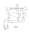
Figure 3 can achieve binary-weighted currents in a similar way to that of the circuitry inFigures 1 and2 . - It is also known in DACs to use a so-called segmented architecture.
Figure 4 shows an overview of a previously considered segmented DAC. The DAC inFigure 4 is part of a DAC integrated circuit (IC) of the current-steering type, and is designed to convert an m-bit digital input word (D1-Dm) into a corresponding analogue output signal. - Referring to
Figure 4 , theDAC 1 contains analogue circuitry including a number n of identicalcurrent sources 21 to 2n, where n = 2m-1. Eachcurrent source 2 passes a substantially constant current I. The analogue circuitry further includes a number n ofdifferential switching circuits 41 to 4n corresponding respectively to the ncurrent sources 21 to 2n. Eachdifferential switching circuit 4 is connected to its correspondingcurrent source 2 and switches the current I produced by the current source either to a first terminal, connected to a first connection line A of the converter, or a second terminal connected to a second connection line B of the converter. - Each
differential switching circuit 4 receives one of a plurality of digital control signals T1 to Tn (called "thermometer-coded signals" for reasons explained hereinafter) and selects either its first terminal or its second terminal in accordance with the value of the signal concerned. A first output current IA of theDAC 1 is the sum of the respective currents delivered to the first terminals of the differential switching circuit, and a second output current IB of theDAC 1 is the sum of the respective currents delivered to the second terminals of the differential switching circuit. The analogue output signal is the voltage difference VA-VB between a voltage VA produced by sinking the first output current IA of theDAC 1 into a resistance R and a voltage VB produced by sinking the second output current IB of the converter into another resistance R. - The thermometer-coded signals T1 to Tn are derived from the binary input word D1-Dm by digital circuitry including a binary-
thermometer decoder 6. Thedecoder 6 operates as follows. When the binary input word D1-Dm has the lowest value the thermometer-coded signals T1-Tn are such that each of thedifferential switching circuits 41 to 4n selects its second terminal so that all of thecurrent sources 21 to 2n are connected to the second connection line B. In this state, VA=0 and VB=nIR. The analogue output signal VA-VB=-nIR. As the binary input word D1-Dm increases progressively in value, the thermometer-coded signals T1 to Tn produced by thedecoder 6 are such that more of the differential switching circuits select their respective first terminals (starting from the differential switching circuit 41) without any differential switching circuit that has already selected its first terminal switching back to its second terminal. When the binary input word D1-Dm has the value i, the first idifferential switching circuits 41 to 4i select their respective first terminals, whereas the remaining n-idifferential switching circuits 4i+1 to 4n select their respective second terminals. The analogue output signal VA-VB is equal to (2i-n)IR. - Thermometer coding is popular in DACs of the current-steering type because, as the binary input word increases, more current sources are switched to the first connection line A without any current source that is already switched to that line A being switched to the other line B. Accordingly, the input/output characteristic of the DAC is monotonic and the glitch impulse resulting from a change of 1 in the input word is small.
- In practice, it is not usual to apply the segmented architecture to all bits of the DAC since to do so would require very large numbers of segments. Accordingly, the segmentation is usually applied only to the most significant bits of the DAC, for example the six most significant bits. This requires a total of 63 identical segments. For the remaining bits of the DAC (the least significant bits or LSBs), a non-segmented architecture is typically used. In this case, the currents for the LSBs need to be scaled appropriately relative to the currents in the MSB segments. In other words, the highest LSB will have a current of half each of the MSB segments, second-highest LSB will have a current of one quarter of each of the MSB segments, and so on. One possibility is to use in each LSB circuit circuitry that is basically the same as the circuitry in each MSB segment. The circuitry will typically comprise at least a current source or current sink and a selection switch. Also, depending on the application of the DAC, each MSB segment may also have other components, for example output cascodes, current bleed circuits, and so on. Because the currents flowing in the LSB circuits are scaled down in comparison with the currents flowing in each MSB segment, it follows that it is necessary to scale all of the corresponding components in the LSB circuits. For example, not only must the current source or sink be scaled, but so also must be the selection switch and any associated cascode.
- Such scaling of the components in the LSB circuits presents several problems. Firstly, there is a tendency to hit minimum device sizes so full scaling may not be possible for the lower LSBs. Furthermore, the output routing capacitance within the LSB circuits does not scale as compared to the MSB segments. These problems translate into unmatched switching delays for each LSB compared to other LSBs and also compared to the MSB segments. Such unmatched switching delays lead in turn to distortion in the output of the DAC.
- The same kind of scaling problems arise even if the LSB circuits are designed differently from the MSB segments. For example, it has been proposed to use a segmented architecture for the MSBs and an R-2R ladder arrangement of the kind shown in
Figure 2 for the LSBs. The R-2R ladder arrangement causes the currents for the LSBs to be scaled relative to the currents in the MSB segments. However, even in this case, the LSBs have a different architecture from the MSB segments. Accordingly, it is difficult in practice to match the switching delays for the LSBs compared to each other and compared to the MSB segments. - According to an embodiment of a first aspect of the present invention, there is provided segmented circuitry comprising: a plurality of mutually-similar segments, including at least two first segments and a second segment, each said segment having signal changing means operable to change a magnitude of a controllable signal of the segment in dependence upon a control signal, each said first segment being connected operatively to a first node of the circuitry and each said second segment being connected operatively to a second node of the circuitry; and impedance ladder means, including a first load element connected between said first node and a load line and a second load element connected between said second node and said load line and a divider element connected between said first and second nodes, for producing a weighted combination of the controllable signals of the plurality of segments, a contribution of said second segment to said weighted combination being 1/k of a contribution of each said first segment, where k is a scaling factor.
- Advantageously, the segments are mutually similar to one another. For example, they may be formed of the same basic circuit elements (e.g. a current source and a load element) connected together in the same basic manner. This means that any mismatches between different segments (for example switching delay mismatches) should be minimised. It will appreciate that in this way such mismatches can be minimised not only between the two first segments, but also between the first segments and the second segment.
- Also by having mutually similar segments, the same type of control signal can be used for each segment, and further the magnitude of the controllable signal of each segment can be controllable in the same way in each segment. For example, given the same control signal to each segment, the segments can advantageously be arranged such that the controllable signal has the same magnitude in each cell. Firstly, this is advantageous from a system design point of view; similar circuitry can be repeated per segment throughout the segmented circuitry. Secondly, this leads to improved minimisation of mismatches between the segments. Thirdly, it is advantageous that the controllable signal in the second segment can have the same magnitude as the controllable signal in the first segments (given the same applied control signal), even though the contribution of the second segment to the weighted combination is 1/k of a contribution of each first segment, where k is a scaling factor. Otherwise, it could be imagined that the controllable signal in the second segment would need to have a
magnitude 1/k times that of the controllable signal in the first segments (given the same applied control signal), which as k increases could lead to a very small such magnitude in the second segment, which is disadvantageous from a switching-delay mismatch point of view. - The segmented circuitry is further advantageous because the available resolution in the weighted combination of the controllable signals can be increased in a simple manner, by adding an extra stage or stages in the impedance ladder means (i.e. to have one or more third segments, or fourth segments etc). The available resolution can also be changed in a simple manner by varying the number of segments at each such stage, i.e. the number of first segments, second segments, third segments, etc. With these two ways of varying the resolution in the weighted combination of the controllable signals, the design of the segmented circuitry can be optimised from the point of view of the number segments employed, and the number of stages in the impedance ladder means (each such stage having, for example, 1/k of a contribution to the weighted combination of the controllable signals of the contribution of the preceding stage). For example, it is advantageous both to minimise the overall number of segments and to minimise the ratio between the contribution to the weighted combination of the controllable signals made by the first segments and the contribution made by the segment (or segments) in the final stage of the impedance ladder means, i.e. to minimise the number of stages in the impedance ladder means. The segmented circuitry of embodiments of the present invention enables this optimisation to be performed whilst maintaining low mismatch between segments.
- Preferably, the segmented circuitry is configured such that: the plurality of mutually-similar segments also includes a third segment, the third segment also having such signal changing means operable to change a magnitude of a controllable current of the segment in dependence upon a control signal, and the third segment being connected operatively to a third node of the circuitry; and the impedance ladder means further includes a third load element connected between said third node and said load line and a further divider element connected between said second and third nodes, such that a contribution of said third segment to said weighted combination is 1/k of said contribution of said second segment. Such a third segment forms an extra stage in the impedance ladder means as mentioned above. By having a third such stage, it is possible to increase the available resolution in the weighted combination of the controllable signals to a certain level by employing fewer segments than would be required if that level was obtained with only two such stages.
- Preferably, the segmented circuitry is configured such that: said plurality of mutually-similar segments also includes one or more further segments, each said further segment having such signal changing means operable to change a magnitude of a controllable signal of the segment in dependence upon a control signal and each said further segment being connected operatively to a corresponding further node of the circuitry; and said impedance ladder means further includes a further load element connected between each said further node and said load line and also includes a further divider element connected between each said further node and the preceding node. Such further segments form further stages in the impedance ladder means as mentioned above. Again, by having a such further stages, it is possible to increase the available resolution in the weighted combination of the controllable signals to a certain level by employing fewer segments than would be required if that level was obtained with fewer such stages.
- Preferably, at least one of the second and subsequent nodes, if any, has two or more such segments connected operatively to the node concerned. By having two or more segments per stage, it is possible to increase the available resolution in the weighted combination of the controllable signals to a certain level by employing fewer such stages than would be required if that level was obtained with one segment per.
- Preferably, the segments are arranged in segment groups, each segment group comprising the same number of segments, the segments of each group being connected operatively to the same one of said nodes. It is advantageous to employ such segment groups of the same size from a system design point of view. Similar groups of circuitry can be employed across the segmented circuitry.
- Preferably, the number of said segment groups for the first segments is greater than the number of segment groups for said second and any subsequent segments. By having effectively more first segments than segments in other stages of the impedance ladder means, it is possible to achieve a certain level of available resolution in the weighted combination of the controllable signals by having fewer such stages than if the same number of segment groups was employed at each such stage.
- An impedance of the or each said divider element may be (k-1)2/k times an impedance of the or each said load element. A last one of said nodes of the circuitry (i.e. a final such stage) may be connected to the load line by a terminating element. An impedance of the terminating element may be k-1 times an impedance of the or each said load element.
- Preferably, each said divider element comprises a resistance element and a bridge capacitor connected in parallel with the resistance element. This arrangement can be configured to reduce a variation in the scaling factor k with frequency, particularly at high frequencies, such as from 3 to 6GHz. For example, a capacitance of the bridge capacitor may be at least k/(k-1)2 times a parasitic capacitance of a resistance element in each said load element. A capacitance of the bridge capacitor may preferably be selected so as to compensate for losses at high frequency arising from capacitances (e.g. parasitic capacitances) of, or associated with, the segments.
- The or each said divider element and each said load element preferably comprises a plurality of mutually-similar unit resistance elements. By using mutually-similar unit resistance elements, matching between segments and between stages of the impedance ladder means can be advantageously high. Preferably, a number of said unit resistance elements in the or each said divider element is the same as a number of said unit resistance elements in each said load element, the unit resistance elements of the or each said divider element being interconnected differently from the unit resistance elements of each said load element so that the or each said divider element has a different impedance from each said load element. In this way, it can be ensured that the best trade-off between total parasitic capacitance of, and mismatch between, the load elements and divider elements is achieved.
- As will be appreciated later herein, in the present invention the relationship between the load elements ZL and the divider elements ZDIV is preferably ZDIV = ((k-1)2/k)ZL, where k is a scaling factor. In order to get best matching for a given area of resistance, it is desirable to employ unit resistance elements all having the same resistance R. In order to optimise the matching between two resistance elements (in this case, between the load and divider elements), they should have the same area as one another. Accordingly, the two elements should preferably have the same number of unit resistance elements as one another, interconnected differently as mentioned above to create the required resistance values. The present invention therefore poses a problem as to how to provide the relationship ZDIV = ((k-1)2/k)ZL using unit resistance elements.
- It can be appreciated that it would be possible to interconnect P*Q unit resistance elements (where P and Q are integers) such that, in a first case, there are P parallel branches each having Q elements in series (hereinafter PpQs), and in a second case, there are Q parallel branches each having P elements in series (hereinafter QpPs). In that way, two resistances having a resistance ratio [P2/Q2]:1 are generated using the same number (P*Q) of unit resistance elements. The required ratio in the present case is of course [(k-1)2/k]:1. Accordingly, it can be seen that scaling factors k, for which k is a perfect square (i.e. k = Q2), enable the desired ratio (k-1)2/k to be achieved by interconnecting P*Q unit resistance elements in the PpQs and QpPs arrangements. That is, values of k of 4, 9, 16, 25, 36, etc are preferable. It will be appreciated that k=4 is preferable from the point of view of minimising the number of such unit resistances required.
Figures 11 (A) and 11 (B) present the two resistor arrangements when k=4. - Preferably, each segment has first and second such controllable signals and said signal changing means in each said segment are operable to change respective magnitudes of said first and second controllable signals of the segment in dependence upon said control signal, and the circuitry has first and second sets of nodes, each said set having such first and subsequent nodes, and the circuitry also has first and second such impedance ladder means, said first impedance ladder means being operable to produce such a weighted combination of the first controllable signals of the plurality of segments and said second impedance ladder means being operable to produce such a weighted combination of the second controllable signals of the plurality of segments. Such segmented circuitry in this way can have differential outputs, an output signal of the circuitry being a difference between the weighted combination of the first controllable signals and the weighted combination of the second controllable signals. Such differential output circuitry is advantageous for the following reasons at least. Firstly, because the output signal of the circuitry is effectively a difference between two signals, small changes in ground potential between such circuitry and a receiver of the output signal do not affect the receiver's ability to detect the signal. Secondly, in systems that employ low supply voltages, problems with signalling can occur because of consequentially-reduced noise immunity. Differential signalling helps to reduce these problems because, for a given supply voltage, it gives twice the noise immunity of a single-ended system. Thirdly, the output signal can be transmitted on balanced lines. A balanced line reduces the noise on a connection by rejecting common-mode interference. Its two wires are routed in parallel so that they receive the same interference. They also have the same impedance to ground, so the interfering fields or currents induce the same voltage in both wires. Since the receiver responds only to the difference between the wires, it is not influenced by the induced noise voltage.
- The or each said controllable signal may be a current, or a voltage. In the case of a current, each said segment may comprise a current source or sink connected to a common node of the segment and at least one first switch connected between said common node and a first output node of the segment and at least one second switch connected between said common node and a second output node of the segment.
- Preferably, there may be in each segment two or more such first switches and two or more such second switches, and further means for controlling the first and second switches such that at each switching event the same number of switches change state. Each such segment may further comprise means for reducing an output impedance at each said output node.
- It will be appreciated that such segmented circuitry could form a digital-to analogue converter (DAC) or a segmented programmable current generator.
- According to an embodiment of a second aspect of the present invention, there is provided a digital-to-analogue converter (DAC) comprising segmented circuitry according to the aforementioned first aspect of the present invention, wherein the control signals for the first segments are derived from first bits of a digital input signal of the converter, and the control signal for the or each said second segment is derived from one or more second bits of said digital input signal, the or each said second bit being less significant than each first bit. Such a DAC may operate at a sample rate of around 12GSa/s.
- According to an embodiment of a third aspect of the present invention, there is provided a segmented programmable current generator comprising segmented circuitry according to the aforementioned first aspect of the present invention, wherein the control signals for the first segments are derived from first bits of a digital input signal of the converter, and the control signal for the or each said second segment is derived from one or more second bits of said digital input signal, the or each said second bit being less significant than each first bit.
- It is envisaged that the present invention may extend to further such aspects. Circuitry embodying the present invention may be provided in the form of an integrated circuit (IC) chip or chipset. According to an embodiment of a further aspect of the present invention there is provided an IC chip or chipset comprising circuitry according to any of the above-mentioned aspects of the present invention. Such an IC chip or chipset may be a small-geometry CMOS IC chip or chipset. Circuitry embodying the present invention may form part of an RF transmitter, for example part of a DAC of an RF transmitter. According to an embodiment of a further aspect of the present invention there is provided an RF transmitter comprising circuitry or an IC chip or chipset (as the case may be) according to any of the above-mentioned aspects of the present invention.
- Reference will now be made, by way of example, to the accompanying drawings, in which:
-
Figure 1 shows a circuit diagram of an R-2R ladder; -
Figure 2 shows a first example of a DAC employing an R-2R ladder architecture; -
Figure 3 shows a second example of a DAC employing an R-2R ladder architecture; -
Figure 4 shows an example of a DAC employing a segmented architecture; -
Figure 5 shows parts of a DAC embodying the present invention; -
Figure 6 shows parts of another DAC embodying the present invention; -
Figure 7 shows parts of theFigure 6 DAC in more detail; -
Figure 8 shows parts of a DAC according to a first embodiment of the present invention; -
Figure 9 shows an overall connection arrangement of theFigure 8 parts; -
Figure 10 shows a possible implementation of a divider element in theFigure 8 DAC; -
Figures 11 (A) and 11 (B) show possible implementations of resistance elements in theFigure 8 DAC; and -
Figure 12 shows parts of a DAC according to a second embodiment of the present invention. -
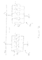
Figure 5 shows parts of segmented mixed-signal circuitry 20 embodying the present invention. Thecircuitry 20 is, for example, part of a DAC. - The
circuitry 20 comprises a plurality of mutually-similar circuitry segments 22. The circuitry segments comprise at least two first segments 22-1 which are connected to a first node N1 of the circuitry. The circuitry further comprises a second segment 22-2 connected to a second node N2 of the circuitry. In addition to the plural first segments 22-1 and the second segment 22-2 it is also possible to provide further segments. For example, as shown in the dotted lines inFigure 5 , a third segment 22-3 can be connected to a third node N3. - Each of the
circuitry segments 22 can be constituted in many different ways and what is shown in each segment inFigure 5 is merely an equivalent circuit of a segment. This equivalent circuit comprises acurrent source 24 connected in parallel with a load impedance ZL. - The first node N1 is connected to the second node N2 by a divider element having an impedance ZDIV. Similarly, the node N2 is connected to the node N3 via a divider element having the same impedance ZDIV. The last of the nodes in the circuitry is connected to ground via a termination element having a termination impedance ZTERM.
- The first node N1 is connected to an output node OUT of the DAC.
- In general, in the present invention the relationship between the load impedance ZL, the divider impedance ZDIV and the termination impedance ZTERM is as follows:


where k is a scaling factor. - In the minimum case shown in
Figure 5 , where there is only one segment connected to each of the second and subsequent nodes N2, N3 etc, the scaling factor k should be set to 2. In this case, ZDIV = ½ ZL and ZTERM = ZL. It will be observed that these are the same impedance ratios as in theFigure 1 circuitry described in the introduction. - When the impedances are set in the manner described above, the impedance looking from the right-hand-side of each of the nodes N1, N2 and N3 into the divider element (or termination element) is (k-1)ZL, i.e. ZL when k = 2. Thus, Z1R, Z2R and Z3R in
Figure 5 are each ZL when k=2. - Also, the impedances looking into each of the nodes N2, N3 etc (but not N1 as noted below) from the left-hand-side are ((k-1)/k)ZL. In the case in which k=2, these impedances are ½ ZL. Thus, Z2L, Z3L etc in
Figure 5 are ½ ZL when k=2. - Because there are plural first segments 22-1 connected to the first node N1, the impedance Z1L looking into the node N1 from the output node OUT is not the same as Z2L or Z3L. The impedance Z1L is the parallel combination of the load impedances ZL in the first segments and Z1R. Thus, Z1L=(k-1)/(i+k-1), where i is the number of first segments 22-1.
- In the
Figure 5 circuitry, the output signal at the output terminal OUT is a weighted combination of the respective signals produced by the individual segments. In the weighted combination, the contribution of the second segment 22-2 is 1/k of the contribution of each first segment 22-1. Similarly, the contribution of the third segment 22-3 is 1/k of the contribution of the second segment. - Each first segment produces its segment signals in dependence upon two or more first bits of the digital input signal applied to the DAC. The second segment produces its segment signal in dependence upon a further bit of a digital input signal. This further bit is the next less significant bit after the least significant bit among the first bits. The third segment produces its segment signal in dependence upon the next bit after the further bit.
- An advantage of the
Figure 5 circuitry is that each of the segments has the same basic elements (thecurrent source 24 and load element ZL). This means that the mismatches between different segments should be minimised. For example, the mismatch in switching delays between the different segments 22-2 and 22-3 should be reduced. Also, the mismatch between the switching delays of each of these LSB segments and each of the MSB segments 22-1 should also be reduced. - Another advantage is that adding extra resolution to the DAC becomes relatively easy, since all that is necessary is to provide extra stages in the ladder arrangement, rather than scaling the components.
-
Figure 6 shows another example of parts of DAC circuitry embodying the present invention. TheFigure 6 circuitry 30 differs from theFigure 5 circuitry 20 in that a plurality of second segments 22-2 are connected to the second node N2 and a plurality of third segments 22-3 are connected to the third node N3. The second segments 22-2 together constitute a segment group SG2 for the node N2. Similarly, the third segments 22-3 together constitute a segment group SG3 for the third node N3. - Because there are plural segments in each of the segment groups SG2 and SG3, these segment groups can be used to process more than one bit of the digital input signal. For example, each of the segment groups SG2 and SG3 may be used to process two or three bits of the digital input signal. Thus, the segment group SG3 is shown as receiving plural bits B3 of the digital input signal, and the segment group SG2 is shown as receiving plural bits B2 of the binary input signal.
- Of course, in practice, the bits of the digital input signal will not normally be applied directly to the segments. Typically, the bits will be decoded by a suitable decoder, such as a binary-to-thermometer decoder (as described previously with reference to
Figure 4 ). The decoder generates thermometer-coded signals for each segment based on the relevant bits of the digital input signal. When thermometer coding is used, and the number of binary bits is 2, the number of segments in each segment group SG2 and SG3 should be 3. When the number of binary bits is 3, the number of segments in the segment groups should be 7. Incidentally, the number of segments required is 2n-1, rather than 2n, because for one of the binary input values (e.g. all zeros) no segment signal is required. In practice, more than the minimum number of segments may be provided, for example so that a segment can be isolated from the remaining parts of the circuitry for calibration purposes whilst still leaving the required minimum number available for processing the digital input signal. Also, as explained later, it is desirable for each segment group to have the same number of segments. This may also make it desirable to include more segments in each group, e.g. 2n segments, even if no spare "calibration" segment is required. - In the
Figure 6 circuitry, the scaling factor k is increased because plural segments are attached to each of the nodes N2 and N3. For example, if the number of bits in each of B2 and B3 is 2, then k should be set to 4 so that the outputs of the second segments 22-2 are scaled by a factor of 4 relative to the outputs of the first segments 22-1 and so that the outputs of the third segments 22-3 are scaled by a factor of 16 relative to the outputs of the first segments 22-1. - In
Figure 6 , plural first segments 22-1 are again connected to the first node N1. In this case, however, the number of first segments is greater than the number of segments in the segment group SG2 and in the segment group SG3. This is not essential, and the number of first segments 22-1 could be equal to the number of segments in the segment groups SG2 and SG3. For reasons that will be explained later, it is preferable to organise the first segments 22-1 as plural segment groups SG11 to SG1j. Each of the segment groups SG11 to SG1j has the same number of segments as each of the segment groups SG2 and SG3. For example, the number of segments in each segment group may be four. - To give a concrete example, the case of a ten-bit DAC will be considered. In this case, the six MSBs are processed by the first segments 22-1. In this case, 64 first segments are provided (63 working segments and 1 segment for calibration). These 64 segments are organised as 16 segment groups SG11 to SG116.
- The two highest-order LSBs (the bits B2 in
Figure 6 ) are processed by the second segments 22-2 in the segment group SG2. Four segments are provided in the group SG2 (3 working segments and 1 for calibration). Similarly, the two lowest-order LSBs (the bits B3 inFigure 6 ) are processed by the third segments 22-3 in the segment group SG3. Again, four segments are provided in the segment group SG3 (3 working segments and 1 for calibration). - It can be seen that in
Figure 6 , the segments in each segment group SG have their respective load impedances ZL connected in parallel between the relevant node N1/N2/N3 and ground. Because of this, it is possible for a segment group SG to share a load element having a load impedance ZLG.Figure 7 shows the first segment groups SG11 to SG1j connected to node N1. Four first segments 22-1 (now not having loads ZL of their own) are connected in parallel between an output node O11 of the segment group SG11 and ground. A sharedload element 32 is also connected between the output node O11 for the segment group and ground. The same is true for each of the other first segment groups SG11 to SG1j. For the first segment groups SG11 to SG1j, the corresponding output nodes O11 to O1j are of course connected together to form node N1. The segment group SG2 can also have a sharedload element 32 connected in parallel with the segments of its group. Similarly, the segment group SG3 can also have a sharedload element 32 connected in parallel with the segments of its group. It will be appreciated that although sharedload elements Z LG 32 are shown inFigure 7 connected between the output nodes for the segment group concerned and ground, they could equivalently be shown connected instead between an upper reference supply VTOP and their respective output nodes, as will be appreciated in respect ofFigure 8 . - The impedance ZLG required of each shared load element is ((k-1)2/k)ZLG. Similarly, ZTERM = (k-1)ZLG in this case.
- It may be preferable to provide a shared load element for each segment group because, depending on the particular process (technology) used to fabricate the chip, a shared load element (having a smaller impedance than a per-segment load element) may be easier to fabricate. In particular, a per-segment load element may need to have a relatively large impedance (resistance), which will have an undesirably large area and hence a large parasitic capacitance. However, the use of per-segment load elements in the
Figure 6 circuit is still possible, and may be preferable in certain fabrication processes. -
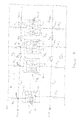
Figure 8 shows an example constitution of one of thesegments 22 in a first embodiment of the present invention. In this embodiment, the DAC is a differential DAC and has first and second output nodes. Each of these output nodes effectively corresponds to the output node OUT shown inFigure 5 andFigure 6 . - Each segment comprises first and second main switching transistors 36-1 and 36-2. The respective sources of the main switching transistors 36-1 and 36-2 are connected to a common node TAIL of the segment. A
current sink 42 is connected between the common node TAIL and ground. This current sink causes a constant current I to flow through the node TAIL in use of the DAC. Mutually-complementary drive signals SW1 and SW2 are applied to the gates of the main switching transistors 36-1 and 36-2. - The drain of the first main switching transistor 36-1 is connected to the source of a first cascode transistor 341. The drain of the second main switching transistor 26-2 is connected to the source of a second cascode transistor 342. A gate of the first cascode transistor 341 is connected to a positive supply line VTOP of the DAC. The second cascode transistor 342 has its drain connected to a second output node ON2 of the segment and its gate connected to the supply line VTOP. A first bleed current sink 401 is connected to the source of the first cascode transistor 341 and a second bleed current sink 402 is connected to the source of the second cascode transistor 342.
- The respective first output nodes ON1 of the segments within the same segment group SG are connected together by a first line L1. The line L1 is also connected to the positive supply line VTOP by a first shared
load element 321. Similarly, the respective second nodes ON2 of the segments within the same segment group are connected together by a second line L2. The line L2 is also connected to the positive supply line VTOP by a second sharedload element 322. Each of the first and second sharedload elements load element 32 shown inFigure 7 . Each sharedload element -
Figure 9 shows how the different segment groups are interconnected in the first embodiment. The first sharedload elements 321 form part of a first impedance ladder arrangement 501. This first ladder arrangement has nodes N1, N2 and N3 as described previously. The first and second nodes N1 and N2 are interconnected by a divider element having impedance ZDIV. Similarly, the second and third nodes N2 and N3 are connected together by a divider element having the impedance ZDIV. The third node N3 is connected to the positive supply line VTOP by a termination element having the impedance ZTERM. The respective first lines L1 of each of the first segment groups SG11 to SG1j are connected in common to the first node N1 of the first ladder arrangement 501. The line L1 of the second segment group SG2 is connected to the second node N2 of the ladder arrangement 501. The line L1 of the third segment group SG3 is connected to the third node N3 of the first ladder arrangement 501. The first sharedload elements 321 of all the segment groups therefore form part of the first ladder arrangement 501. - The
Figure 9 DAC also comprises a second impedance ladder arrangement 502. This second ladder arrangement comprises the respective second sharedload elements 322 of all of the segment groups. This second ladder arrangement 502 has first, second and third nodes N1, N2 and N3 similar to the first ladder arrangement 501. The respective second lines L2 of the first segment groups SG11 to SG1j are connected in common to the first node N1 of the second ladder arrangement 502, the second line L2 of the second segment group SG2 is connected to the node N2 of the second ladder arrangement 502, and the second line L2 of the third segment group SG3 is connected to the third node N3 of the second ladder arrangement 502. The second ladder arrangement 502 also has the divider elements and termination element just as in the first ladder arrangement 501. - It is emphasised that
Figure 9 is schematic in nature, the two impedance ladder arrangements 501 and 502 being shown above and below the segments merely so that their equivalence to one another can be clearly seen. For example, ground connections of the segments are not shown inFigure 9 , and accordingly the representation of the segments inFigure 9 differs from that in, for example,Figure 7 . Effectively,Figure 9 is intended to show the two sets of signal paths of the impedance ladder arrangements. - Operation of the embodiment of
Figures 8 and9 will now be described. Eachsegment 22 receives a corresponding pair of mutually-complementary drive signals SW1 and SW2 from a binary-to-thermometer decoder (not shown). According to the states of the complementary drive signals SW1 and SW2, one of the main switching transistors 36-1 and 36-2 in each segment is turned ON and the other of those two transistors is turned OFF. Accordingly, the current I flows either through the transistor 36-1 or the transistor 36-2. Each of the cascode transistors 341 and 342 is maintained permanently on and in the saturated condition because the gate of each cascode transistor is connected to VTOP. The bleed current sinks 401 and 402 ensure that sufficient current flow is maintained through each of the cascode transistors even when the transistor 36-1 or 36-2 to which it is connected is turned off. For example IBLEED may be around one quarter of I. - Accordingly, at any given time, IBLEED+I is drawn into the segment from one of the two output nodes ON1 and ON2 and IBLEED is drawn from the other output node. The output node which has I+IBLEED is determined by the switching state of the segment concerned. The current drawn into the segment through the first output node ON1 is a first controllable signal of the segment. The current drawn into the segment through the second output node ON2 is a second controllable signal of the segment. The magnitudes of the first and second controllable signals are controlled by the switching signals SW1 and SW2 applied to the segment.
- Because the first output nodes of the segments within a segment group are connected together by the line L1, the currents drawn through the first output nodes are summed. Similarly, the currents drawn through the second output nodes of the segments within the segment group are also summed because of the interconnection of those nodes by the line L2. The effect of the first impedance ladder network 501 is to scale the contribution of each second segment 22-2 in the second segment group SG2 by the scaling factor k in relation to that of each first segment 22-1 in any of the first segment groups SG11 to SG1j. Similarly, the contribution to the output voltage at the output terminal OUTA of each third segment 22-3 in the segment group SG3 is scaled by the factor k2 as compared to the contribution of each first segment.
-
Figure 10 shows an example of the implementation of each of the ZDIV in the present invention. As shown inFigure 10 , each divider element comprises aresistance element 62 and abridge capacitor 64 connected in parallel with theresistance element 62. Thecapacitor 64 is used to compensate for the capacitance associated with the load elements (321 and 322). Because ZDIV = ((k-1)2/k)ZLG, the capacitance of the bridge capacitor should be at least k/(k-1)2 times the capacitance of eachload element - It is also possible to trim the capacitors 64 (increasing them slightly) to compensate for any parasitic capacitances associated with the resistors. These resistor parasitic capacitances cause losses at high frequencies of signals propagating along the series of nodes N1 to N3 in each impedance ladder arrangement in the direction to the output terminal. Provided that the parasitic capacitances are moderate, the effect of the losses can be compensated for by increasing the capacitance of the bridge capacitor slightly. Thus, the capacitance C64 of the bridge capacitance should be (kcdiv.k)/(k-1)2 times the capacitance of each
load element - In embodiments of the present invention, it is important for the load elements, divider elements and termination elements to have matching impedances (resistances).
Figures 11 (A) and 11 (B) show a preferred way of achieving such matching. In this example, it is assumed that the scaling factor k is 4. In this case, it is required that ZDIV = (9/4).ZLG. In this example, it will be assumed that the number of first segment groups is 16 and that a target output impedance of the DAC is 25Ω. In this case, because 16 sharedload elements 321 are connected to the output terminal OUTA and 16 sharedload elements 322 are connected to the second output terminal OUTB, it follows that ZLG should be 16 x 25 = 400Ω. At any one time, only 63 of the 64 MSB segments are in use (the 64th being calibrated), and the LSB segments collectively serve as a 64th segment. The MSB segments together contribute, in the present example, 63/64 of the output range, and the LSB segments together contribute 1/64 of the output range. It follows that ZDIV should be 900Ω. - In this case, the
resistance element 62 in eachdivider element 60 can be implemented using 6 unit resistances 70, each having a resistance R of 600Ω. Theresistance element 62 inFigure 11(A) has three parallel branches. Each branch has two unit resistances 70 connected in series. The resulting overall resistance is 400Ω. - Similarly, the resistance element in each
divider element 60 can be implemented as shown inFigure 11 (B) . In this case, theresistance element 62 has two parallel branches, each branch having three of the unit resistances 70 connected in series The resulting impedance is 900Ω. - Because the unit resistances 70 in the load elements and divider elements are the same, accurate matching of the resistance values of the load elements and divider elements is obtainable. This is possible because the unit resistances have the same width and length, thereby eliminating width and length effects.
- The following explanation relates to one possible process (technology) only and explains how the resistances and bridge capacitors can be implemented in this particular process.
- For example, it is envisaged that the unit resistances might be implemented in the chosen process using non-silicided polysilicon. Non-silicided polysilicon has a resistance of 450Ω/∼. The maximum current permitted in such a resistor is 0.28mA/µm. It is assumed that each first segment group SG11 to SGIj is capable of causing a maximum current of 1.25mA to flow through the node N1 (this corresponds to a full scale output current of 16 x 1.25mA = 20mA). This means that the
load elements Figure 11 (A) , each of theload elements 32 is constituted by 3 parallel branches. The maximum current in each branch is 1.25mA/3 = 0.42mA. This means that the minimum width of each of the unit resistances 70 is 1.48µm. Because each unit resistance 70 is required to have a resistance of 600Ω, in non-silicided polysilicon this corresponds to 1.33 -. This corresponds to a minimum length of 1.33 x 1.48 = 1.98 µm. The area of each unit resistance is then 3 µm2. The total area occupied by each of theresistors - One of the constraints in designing circuitry embodying the present invention is the accuracy of the resistors. Generally, the mismatch between resistors is inversely proportional to the square root of the area of the resistor. For example, for non-silicided polysilicon resistors the mismatch (standard deviation σ) may be 1.33%/√A, where A is the resistor area. If A = 18 µm2, then σ = 0.31%. Taking a practical example in which the DAC has 12 bits, with 6 MSBs (B1 in
Figure 6) and 6 LSBs (B2 + B3 inFigure 6 ), the required accuracy is 100%/64 = 1.6%, which is around 5σ. Typically, a 3σ figure can be used, i.e. 0.9%, which is around ½ an LSB. Effectively, this means that 13-bit accuracy (linearity) can be expected. Incidentally, in principle it is possible to calibrate out the effects of resistor mismatches, e.g. by adjusting the currents produced by the current sources in individual segments. However, it appears that this is not necessary in practice, because the expected accuracies exceed the presently-contemplated numbers of bits. - The larger the resistors, the larger their parasitic capacitances. However, it appears that in practice the parasitic capacitances of the resistors are less than half the parasitic capacitances of the output transistors (134-1 and 134-2) in the segments (see
Figure 12 ). - As already mentioned in respect of
Figure 10 , each divider impedance ZDIV is implemented as a resistor in parallel with a bridge capacitor such that the scaling factor k is constant across all frequencies. Also as already mentioned, it is possible to apply a compensation factor kcdiv to the value of the bridge capacitances in order to compensate for parasitic capacitances. In order to explore this further, the following analysis has been carried out. - For this analysis, it is assumed that the target output resistance of the DAC is 25Ω, and allowance is made in the DAC output capacitance of 0.2pF for ESD circuitry, 0.2pF for the DAC transistors, and 0.2pF for the tracking in the DAC.
- Accordingly, taking into account the parasitic capacitance for the DAC transistors and the tracking, amounting to 0.4pF, and given 16 segment groups in the DAC, this amounts to 25fF (0.4pF/16) output capacitance for each segment group.
- Considering just the output capacitance due to the tracking and DAC transistors, calculations show that the loss experienced is around -0.24dB at 6GHz (which, given a 12 GSa/s DAC, is the highest frequency of concern). Considering just the output capacitance due to the resistances, calculations show that the loss experienced is around -0.18dB at 6GHz. Considering the output capacitance due to the tracking, DAC transistors and the resistances, calculations show that the loss experienced is around □ 0.4dB at 6GHz. This is an error of 4%, which equates to 12-bit accuracy with about 2.5 LSBs error. This is much larger than the desirable <1 LSB error at 12-bit accuracy.
- If the bridge capacitors of ZDIV are set using compensation kcdiv = 1 (i.e. no compensation), calculations show that the loss experienced as a result of the output capacitance due to the tracking and DAC transistors alone reduces to around 0dB at 6GHz. However, with kcdiv = 1, calculations show that the loss experienced as a result of the output capacitance due to the tracking, DAC transistors and the resistances is only reduced to around 0.16dB at 6GHz.
- Further calculations show that by adjusting the applied compensation to kcdiv = 1.44, the loss experienced due to the output capacitance as a result of the tracking, DAC transistors and the resistances becomes negligible, i.e. reduces to around 0dB at 6GHz. With k = 4 and the resistance ZDIV being 900 Ω as before, this equates to the bridge capacitance in ZDIV being around 16fF (25fF x (4/9) x 1.44). In this situation, with the resistance of ZTERM being 1200Ω as before, this equates to the bridge capacitance in ZTERM being 12fF (16fF x (3/4)).
- Consideration has also been given to the effect of variation in capacitances due to inaccuracies in the processes employed in the manufacture of the DAC. The bridge capacitors could be formed out of metal, in which case variation in capacitance of the bridge capacitances will match variation in parasitic capacitance due to the tracking. Because the contribution of the tracking (0.2pF) to the output capacitance is assumed to be equal to the contribution due to the DAC transistors (0.2pF), a 20% variation in the parasitic capacitance of the DAC transistors relative to the metal capacitances equates to an overall effective 10% error in the value of the bridge capacitances. With 10% error in the value of the bridge capacitances, calculations show that the error in the loss experienced due to the combination of the output capacitance COUT in respect of the tracking and DAC transistors together with the resistances is around ±0.12dB at 6GHz, which equates to 12-bit accuracy with about 0.75 LSB error (i.e. less than 1 part in 64). Further calculations show that the error is around ±0.05dB at 3GHz, which equates to 12-bit accuracy with about 0.3 LSB error, i.e. the DAC will have almost ideal performance to 14-bit accuracy at 3GHz (which is a high enough frequency, for example, for outputting RF signals).
- Overall, considering the target output resistance of 25Ω and the allowed output capacitance of 0.6pF (0.2pF for DAC transistors, 0.2pF for tracking, and 0.2pF for ESD circuitry), calculations show that the DAC can have an output bandwidth of 3dB at 20GHz.
-
Figure 12 shows parts of each of thesegments 22 in a second embodiment of the present invention. Parts inFigure 12 that are the same as the parts in the first embodiment (Figure 8 ) are denoted by the same reference numerals. InFigure 12 , a plurality of main switching transistors are provided for each output node ON1 and ON2 of the segment. Transistors 136-1, 136-3, 136-5 and 136-7 are provided for the first output node ON1. Transistors 136-2, 136-4, 136-6 and 136-8 are provided for the second output node ON2. Also, the arrangement of cascode transistors is changed in comparison to theFigure 8 segment. There are now two cascode transistors per output node. The cascode transistors 1341 and 1343 are provided for the first output node ON 1, and the cascode transistors 1342 and 1344 are provided for the second output node ON2. The upper cascode transistors 1341 and 1342 are provided to eliminate the dependence of the drain potentials of the switching transistors 136 on the potentials of the output nodes ON1 and ON2. This is achieved by taking a tap from a tap point TP1 or TP2 on each of the first and second sharedload elements load element 1321 is coupled to a gate of the cascode transistor 1342. The tap point TP2 from the second sharedload element 1322 is coupled to a gate of the cascode transistor 1341. The potential at the tap point TP1 is a scaled-down version of the potential at the first output node ON1. Similarly, the potential at the tap point TP2 is a scaled-down version of the potential at the second output node ON2. Application of the scaled-down potentials to the gates of the cascode transistors 1341 and 1342 therefore serves to fix their source potentials at values that are substantially independent of the output-node potentials. The further pair of cascode transistors 1343 and 1344 is provided to remove the dependence of the drain potentials of the switching transistors 136 on the switching state of the segment (that is which of the output nodes has the current IBLEED + I and which of them has the current IBLEED). Further details of the arrangement and operation of the cascode transistors 1341 to1344 can be found in the applicant's co-pending patent application [agents ref: P108196EP00/DNL], the entire contents of which are incorporated herein by reference. - Operation of the
Figure 12 embodiment is basically the same as that of theFigure 8 embodiment. However, each segment operates in a repeating sequence of four phases. - In a first phase, one of the transistors 136-1 and 136-2 is turned on and the other is turned off in dependence upon the data for the segment. All of the remaining switching transistors 136-3 to 136-8 are off. In a second phase, one of the transistors 136-3 and 136-4 is turned on and the other is turned off in dependence upon the data signal. The remaining transistors 136-1, 136-2 and 136-5 to 136-8 are all off. In a third phase, one of the switching transistors 136-5 and 136-6 is turned on and the other is turned off in dependence upon the data signal. The remaining transistors 136-1 to 136-4 and 136-7 and 136-8 are off. In a fourth phase, one of the transistors 136-7 and 136-8 is turned on and the other is turned off in dependence upon the data signal. The remaining transistors 136-1 to 136-6 are off.
- The four-phase operation described above has the advantage that the same number of switching transistors change state from one phase to the next, irrespective of whether or not the data signal changes. For example, if in a first phase the switching transistor 136-1 is on and in the next phase the data remains the same, the transistor 136-1 is turned off and the transistor 136-3 is turned on. This kind of operation is not possible in the
Figure 8 embodiment in which there is only one switching transistor 36-1 or 36-2 per output node. By arranging for the same number of switches to change state from one phase to the next, third-order distortion in the DAC is reduced. - Referring to
Figure 9 , it can be seen that the potential at the second node N2 in the first ladder arrangement 501 will be different from the potential at the first node N1 of that ladder arrangement in operation of the circuitry. The same will be true for the nodes N1 and N2 in the second ladder arrangement 502. Similarly, the potentials of the nodes N2 and N3 in each ladder arrangement will differ from one another in operation of the circuitry. This means that, although each of the sharedload elements - Because of this, it is less critical to set the tap points correctly in the second and subsequent segments groups. For example, it would be possible to use the same tap points in the second and subsequent segment groups as are used in the first segment groups. Further, it would be possible to employ a single shared load element (for each of the two outputs) in the DAC (in addition to the
load elements 1321 and 3122 in each segment) and connect the gates of the upper cascode transistors 1341 and 1342 of each segment instead to corresponding shared tap points in the shared load elements. Optionally, it would be possible instead to connect those gates to a constant DC voltage source. Because, as mentioned above, the LSBs are less significant than the MSBs, the tap point in such a single shared load element, or the DC voltage level of the DC voltage source, should preferably be optimised with respect to the MSBs. Further possibilities are set out in the applicant s co-pending patent application [agent s ref: P108196EP00/DNL], the entire contents of which are incorporated herein by reference, and a copy of which was filed with the present application. - Although the present invention has been described in relation to a segmented DAC, it will be appreciated that in other embodiments the invention can be applied in any kind of segmented mixed-signal circuitry. For example, the invention can be applied to digitally-programmable current generators and mixers
- It will also be understood that although in the foregoing embodiments n-channel FET transistors have been used, embodiments of the present invention can also make use of p-channel FETs. In this case the currents flow out of the output terminals/nodes of the circuitry, rather than into them, and the segments contain current source circuits rather than current sink circuits.
- Also, in place of FET transistors, bipolar transistors can be used, as can any other kind of three-terminal current device such as a valve. Effectively, any high-speed current switch can be employed in each segment in order to switch a current between two paths in dependence upon a control signal.
Claims (20)
- Segmented circuitry comprising:a plurality of mutually-similar segments, including at least two first segments and a second segment, each said segment having signal changing means operable to change a magnitude of a controllable signal of the segment in dependence upon a control signal, each said first segment being connected operatively to a first node of the circuitry and each said second segment being connected operatively to a second node of the circuitry; andimpedance ladder means, including a first load element connected between said first node and a load line and a second load element connected between said second node and said load line and a divider element connected between said first and second nodes, for producing a weighted combination of the controllable signals of the plurality of segments, a contribution of said second segment to said weighted combination being 1/k of a contribution of each said first segment, where k is a scaling factor.
- Segmented circuitry as claimed in claim 1, wherein:the plurality of mutually-similar segments also includes a third segment, the third segment also having such signal changing means operable to change a magnitude of a controllable current of the segment in dependence upon a control signal, and the third segment being connected operatively to a third node of the circuitry; andthe impedance ladder means further includes a third load element connected between said third node and said load line and a further divider element connected between said second and third nodes, such that a contribution of said third segment to said weighted combination is 1/k of said contribution of said second segment.
- Segmented circuitry as claimed in claim 2, wherein:said plurality of mutually-similar segments also includes one or more further segments, each said further segment having such signal changing means operable to change a magnitude of a controllable signal of the segment in dependence upon a control signal and each said further segment being connected operatively to a corresponding further node of the circuitry; andsaid impedance ladder means further includes a further load element connected between each said further node and said load line and also includes a further divider element connected between each said further node and the preceding node.
- Segmented circuitry as claimed in any preceding claim, wherein at least one of the second and subsequent nodes, if any, has two or more such segments connected operatively to the node concerned.
- Segmented circuitry as claimed in claim 4, wherein the segments are arranged in segment groups, each segment group comprising the same number of segments, the segments of each group being connected operatively to the same one of said nodes.
- Segmented circuitry as claimed in claim 5, wherein the number of said segment groups for the first segments is greater than the number of segment groups for said second and any subsequent segments.
- Segmented circuitry as claimed in any preceding claim, wherein an impedance of the or each said divider element is (k-1)2/k times an impedance of the or each said load element.
- Segmented circuitry as claimed in any preceding claim, wherein a last one of said nodes of the circuitry is connected to said load line by a terminating element.
- Segmented circuitry as claimed in claim 8, wherein an impedance of said terminating element is k-1 times an impedance of the or each said load element.
- Segmented circuitry as claimed in any preceding claim, wherein each said divider element comprises a resistance element and a bridge capacitor connected in parallel with the resistance element.
- Segmented circuitry as claimed in claim 10, wherein a capacitance of said bridge capacitor is at least k/(k-1)2 times a parasitic capacitance of a resistance element in each said load element.
- Segmented circuitry as claimed in claim 10 or 11, wherein a capacitance of said bridge capacitor is selected so as to compensate for losses at high frequency arising from capacitances of, or associated with, the segments.
- Segmented circuitry as claimed in any preceding claim, wherein the or each said divider element and each said load element comprises a plurality of mutually-similar unit resistance elements.
- Segmented circuitry as claimed in claim 13, wherein a number of said unit resistance elements in the or each said divider element is the same as a number of said unit resistance elements in each said load element, the unit resistance elements of the or each said divider element being interconnected differently from the unit resistance elements of each said load element so that the or each said divider element has a different impedance from each said load element.
- Segmented circuitry as claimed in any preceding claim, wherein each segment has first and second such controllable signals and said signal changing means in each said segment are operable to change respective magnitudes of said first and second controllable signals of the segment in dependence upon said control signal, and the circuitry has first and second sets of nodes, each said set having such first and subsequent nodes, and the circuitry also has first and second such impedance ladder means, said first impedance ladder means being operable to produce such a weighted combination of the first controllable signals of the plurality of segments and said second impedance ladder means being operable to produce such a weighted combination of the second controllable signals of the plurality of segments.
- Segmented circuitry as claimed in any preceding claim, wherein the or each said controllable signal is a current.
- Segmented circuitry as claimed in claim 16, wherein each said segment comprises a current source or sink connected to a common node of the segment and at least one first switch connected between said common node and a first output node of the segment and at least one second switch connected between said common node and a second output node of the segment.
- Segmented circuitry as claimed in claim 17, having two or more such first switches and two or more such second switches, and also having means for controlling the first and second switches such that at each switching event the same number of switches change state.
- Segmented circuitry as claimed in claim 17 or 18, wherein each said segment further comprises means for reducing an output impedance at each said output node.
- A digital-to-analogue converter comprising segmented circuitry as claimed in any preceding claim, wherein the control signals for the first segments are derived from first bits of a digital input signal of the converter, and the control signal for the or each said second segment is derived from one or more second bits of said digital input signal, the or each said second bit being less significant than each first bit.
Priority Applications (1)
| Application Number | Priority Date | Filing Date | Title |
|---|---|---|---|
| EP07113376.3A EP2019490B1 (en) | 2007-07-27 | 2007-07-27 | Segmented circuitry |
Applications Claiming Priority (1)
| Application Number | Priority Date | Filing Date | Title |
|---|---|---|---|
| EP07113376.3A EP2019490B1 (en) | 2007-07-27 | 2007-07-27 | Segmented circuitry |
Publications (2)
| Publication Number | Publication Date |
|---|---|
| EP2019490A1 true EP2019490A1 (en) | 2009-01-28 |
| EP2019490B1 EP2019490B1 (en) | 2018-07-18 |
Family
ID=39650508
Family Applications (1)
| Application Number | Title | Priority Date | Filing Date |
|---|---|---|---|
| EP07113376.3A Active EP2019490B1 (en) | 2007-07-27 | 2007-07-27 | Segmented circuitry |
Country Status (1)
| Country | Link |
|---|---|
| EP (1) | EP2019490B1 (en) |
Cited By (20)
| Publication number | Priority date | Publication date | Assignee | Title |
|---|---|---|---|---|
| EP2019486A1 (en) | 2007-07-27 | 2009-01-28 | Fujitsu Ltd. | RF transmitters |
| US8976050B1 (en) | 2013-09-12 | 2015-03-10 | Fujitsu Semiconductor Limited | Circuitry and methods for use in mixed-signal circuitry |
| EP2849345A1 (en) | 2013-09-12 | 2015-03-18 | Fujitsu Semiconductor Limited | Circuitry and methods for use in mixed-signal circuitry |
| EP2849344A1 (en) | 2013-09-12 | 2015-03-18 | Fujitsu Semiconductor Limited | Circuitry and methods for use in mixed-signal circuitry |
| EP2849021A1 (en) | 2013-09-12 | 2015-03-18 | Fujitsu Semiconductor Limited | Signal-alignment circuitry and methods |
| US9054722B2 (en) | 2013-09-12 | 2015-06-09 | Fujitsu Semiconductor Limited | Circuitry and methods for use in mixed-signal circuitry |
| US9112521B2 (en) | 2013-09-12 | 2015-08-18 | Socionext Inc. | Mixed-signal circuitry |
| US9178524B1 (en) | 2014-05-27 | 2015-11-03 | Qualcomm Incorporated | Hybrid R-2R structure for low glitch noise segmented DAC |
| US9201813B2 (en) | 2013-09-12 | 2015-12-01 | Socionext Inc. | Signal distribution circuitry |
| US9432013B2 (en) | 2013-09-12 | 2016-08-30 | Socionext Inc. | Circuitry useful for clock generation and distribution |
| US9450279B2 (en) | 2013-09-12 | 2016-09-20 | Socionext Inc. | Components and circuits for output termination |
| EP3442123A1 (en) * | 2017-08-08 | 2019-02-13 | NXP USA, Inc. | Digital to analog converter (dac) having sub-dacs with arrays of resistors |
| EP3618282A1 (en) | 2018-08-31 | 2020-03-04 | Socionext Inc. | Current generation |
| US10784886B1 (en) | 2019-09-27 | 2020-09-22 | Nxp Usa, Inc. | Segmented digital to analog converter |
| US10790848B2 (en) | 2018-06-04 | 2020-09-29 | Nxp Usa, Inc. | Segmented resistive digital to analog converter |
| CN113541653A (en) * | 2021-07-27 | 2021-10-22 | 温州大学 | Nanosecond steep edge pulse signal generator based on transmission line reflection principle |
| WO2022026108A1 (en) * | 2020-07-31 | 2022-02-03 | Qualcomm Incorporated | Flash-successive approximation register (sar) hybrid analog-to-digital converter (adc) |
| CN115296671A (en) * | 2022-10-09 | 2022-11-04 | 湖南毂梁微电子有限公司 | Digital-to-analog conversion circuit with mixed structure |
| CN115333540A (en) * | 2022-10-14 | 2022-11-11 | 杰创智能科技股份有限公司 | Digital-to-analog converter resistance selection method, device, equipment and storage medium |
| EP4125217A1 (en) | 2021-07-27 | 2023-02-01 | Socionext Inc. | Calibration and alignment |
Citations (5)
| Publication number | Priority date | Publication date | Assignee | Title |
|---|---|---|---|---|
| US5612696A (en) | 1994-12-03 | 1997-03-18 | Electronics & Telecommunications Research Institute | Digital-to-analog converter of current segmentation |
| US5703586A (en) | 1995-12-07 | 1997-12-30 | Analog Devices, Inc. | Digital-to-analog converter having programmable transfer function errors and method of programming same |
| US20060092065A1 (en) | 2004-10-29 | 2006-05-04 | Broadcom Corporation | Delay equalized z/2z ladder for digital to analog conversion |
| US7173552B1 (en) | 2003-10-01 | 2007-02-06 | Analog Devices, Inc. | High accuracy segmented DAC |
| EP2023489A1 (en) | 2007-07-27 | 2009-02-11 | Fujitsu Ltd. | Current switching circuitry |
-
2007
- 2007-07-27 EP EP07113376.3A patent/EP2019490B1/en active Active
Patent Citations (5)
| Publication number | Priority date | Publication date | Assignee | Title |
|---|---|---|---|---|
| US5612696A (en) | 1994-12-03 | 1997-03-18 | Electronics & Telecommunications Research Institute | Digital-to-analog converter of current segmentation |
| US5703586A (en) | 1995-12-07 | 1997-12-30 | Analog Devices, Inc. | Digital-to-analog converter having programmable transfer function errors and method of programming same |
| US7173552B1 (en) | 2003-10-01 | 2007-02-06 | Analog Devices, Inc. | High accuracy segmented DAC |
| US20060092065A1 (en) | 2004-10-29 | 2006-05-04 | Broadcom Corporation | Delay equalized z/2z ladder for digital to analog conversion |
| EP2023489A1 (en) | 2007-07-27 | 2009-02-11 | Fujitsu Ltd. | Current switching circuitry |
Cited By (27)
| Publication number | Priority date | Publication date | Assignee | Title |
|---|---|---|---|---|
| EP2019486A1 (en) | 2007-07-27 | 2009-01-28 | Fujitsu Ltd. | RF transmitters |
| US9432013B2 (en) | 2013-09-12 | 2016-08-30 | Socionext Inc. | Circuitry useful for clock generation and distribution |
| EP2849344A1 (en) | 2013-09-12 | 2015-03-18 | Fujitsu Semiconductor Limited | Circuitry and methods for use in mixed-signal circuitry |
| US9705475B2 (en) | 2013-09-12 | 2017-07-11 | Socionext Inc. | Circuitry useful for clock generation and distribution |
| US9973186B2 (en) | 2013-09-12 | 2018-05-15 | Socionext Inc. | Circuitry and methods for use in mixed-signal circuitry |
| US9054722B2 (en) | 2013-09-12 | 2015-06-09 | Fujitsu Semiconductor Limited | Circuitry and methods for use in mixed-signal circuitry |
| US9112521B2 (en) | 2013-09-12 | 2015-08-18 | Socionext Inc. | Mixed-signal circuitry |
| US9450279B2 (en) | 2013-09-12 | 2016-09-20 | Socionext Inc. | Components and circuits for output termination |
| US9178523B2 (en) | 2013-09-12 | 2015-11-03 | Socionext Inc. | Circuitry and methods for use in mixed-signals circuitry |
| US9201813B2 (en) | 2013-09-12 | 2015-12-01 | Socionext Inc. | Signal distribution circuitry |
| EP2849021A1 (en) | 2013-09-12 | 2015-03-18 | Fujitsu Semiconductor Limited | Signal-alignment circuitry and methods |
| US9344060B2 (en) | 2013-09-12 | 2016-05-17 | Socionext Inc. | Signal-alignment circuitry and methods |
| US8976050B1 (en) | 2013-09-12 | 2015-03-10 | Fujitsu Semiconductor Limited | Circuitry and methods for use in mixed-signal circuitry |
| EP2849345A1 (en) | 2013-09-12 | 2015-03-18 | Fujitsu Semiconductor Limited | Circuitry and methods for use in mixed-signal circuitry |
| US9178524B1 (en) | 2014-05-27 | 2015-11-03 | Qualcomm Incorporated | Hybrid R-2R structure for low glitch noise segmented DAC |
| WO2015183496A1 (en) * | 2014-05-27 | 2015-12-03 | Qualcomm Incorporated | Hybrid r-2r structure for low glitch noise segmented dac |
| EP3442123A1 (en) * | 2017-08-08 | 2019-02-13 | NXP USA, Inc. | Digital to analog converter (dac) having sub-dacs with arrays of resistors |
| CN109391270A (en) * | 2017-08-08 | 2019-02-26 | 恩智浦美国有限公司 | D/A converter (DAC) with the sub- DAC containing resistor array |
| CN109391270B (en) * | 2017-08-08 | 2023-09-26 | 恩智浦美国有限公司 | Digital-to-analog converter (DAC) with sub-DAC containing resistor array |
| US10790848B2 (en) | 2018-06-04 | 2020-09-29 | Nxp Usa, Inc. | Segmented resistive digital to analog converter |
| EP3618282A1 (en) | 2018-08-31 | 2020-03-04 | Socionext Inc. | Current generation |
| US10784886B1 (en) | 2019-09-27 | 2020-09-22 | Nxp Usa, Inc. | Segmented digital to analog converter |
| WO2022026108A1 (en) * | 2020-07-31 | 2022-02-03 | Qualcomm Incorporated | Flash-successive approximation register (sar) hybrid analog-to-digital converter (adc) |
| CN113541653A (en) * | 2021-07-27 | 2021-10-22 | 温州大学 | Nanosecond steep edge pulse signal generator based on transmission line reflection principle |
| EP4125217A1 (en) | 2021-07-27 | 2023-02-01 | Socionext Inc. | Calibration and alignment |
| CN115296671A (en) * | 2022-10-09 | 2022-11-04 | 湖南毂梁微电子有限公司 | Digital-to-analog conversion circuit with mixed structure |
| CN115333540A (en) * | 2022-10-14 | 2022-11-11 | 杰创智能科技股份有限公司 | Digital-to-analog converter resistance selection method, device, equipment and storage medium |
Also Published As
| Publication number | Publication date |
|---|---|
| EP2019490B1 (en) | 2018-07-18 |
Similar Documents
| Publication | Publication Date | Title |
|---|---|---|
| EP2019490B1 (en) | Segmented circuitry | |
| US6914547B1 (en) | Triple resistor string DAC architecture | |
| US6414616B1 (en) | Architecture for voltage scaling DAC | |
| CN106209108B (en) | Segmented DAC | |
| Van den Bosch et al. | SFDR-bandwidth limitations for high speed high resolution current steering CMOS D/A converters | |
| US6906652B2 (en) | High dynamic linearity current-mode digital-to-analog converter architecture | |
| KR0179466B1 (en) | Self-calibrating high speed d/a converter | |
| EP1257060B1 (en) | Digital-to-analogue converter using an array of current sources | |
| US7501970B2 (en) | Digital to analog converter architecture and method having low switch count and small output impedance | |
| US9100045B2 (en) | Multiple string digital to analog converter | |
| US5446455A (en) | Auto-calibrated current-mode digital-to-analog converter and method therefor | |
| Bastos et al. | A high yield 12-bit 250-MS/s CMOS D/A converter | |
| JP2001244816A (en) | Digitally switched potentiometer with improved linearity and setting time | |
| JPH0566774B2 (en) | ||
| US7304596B2 (en) | Folded multi-LSB decided resistor string digital to analog converter | |
| US20130293405A1 (en) | Segmented digital-to-analog converter having weighted current sources | |
| JP2003124809A (en) | Charge redistribution sequential approximation type analog-to-digital converter (adc) using improved switched capacitor | |
| JP4741680B2 (en) | Flexible analog / digital converter | |
| GB2393055A (en) | A transconductance amplifier with input sampling capacitor for a current-interpolating A-D converter | |
| US6317069B1 (en) | Digital-to-analog converter employing binary-weighted transistor array | |
| US6778122B2 (en) | Resistor string digital to analog converter with differential outputs and reduced switch count | |
| US9143156B1 (en) | High-resolution digital to analog converter | |
| US7554475B2 (en) | Low-power inverted ladder digital-to-analog converter | |
| US8912939B2 (en) | String DAC leakage current cancellation | |
| CN111801894A (en) | Digital-to-analog converter system |
Legal Events
| Date | Code | Title | Description |
|---|---|---|---|
| PUAI | Public reference made under article 153(3) epc to a published international application that has entered the european phase |
Free format text: ORIGINAL CODE: 0009012 |
|
| AK | Designated contracting states |
Kind code of ref document: A1 Designated state(s): AT BE BG CH CY CZ DE DK EE ES FI FR GB GR HU IE IS IT LI LT LU LV MC MT NL PL PT RO SE SI SK TR |
|
| AX | Request for extension of the european patent |
Extension state: AL BA HR MK RS |
|
| 17P | Request for examination filed |
Effective date: 20090727 |
|
| AKX | Designation fees paid |
Designated state(s): DE FR GB |
|
| 17Q | First examination report despatched |
Effective date: 20091130 |
|
| RAP1 | Party data changed (applicant data changed or rights of an application transferred) |
Owner name: FUJITSU MICROELECTRONICS LIMITED |
|
| RAP1 | Party data changed (applicant data changed or rights of an application transferred) |
Owner name: FUJITSU SEMICONDUCTOR LIMITED |
|
| RAP1 | Party data changed (applicant data changed or rights of an application transferred) |
Owner name: SOCIONEXT INC. |
|
| GRAP | Despatch of communication of intention to grant a patent |
Free format text: ORIGINAL CODE: EPIDOSNIGR1 |
|
| STAA | Information on the status of an ep patent application or granted ep patent |
Free format text: STATUS: GRANT OF PATENT IS INTENDED |
|
| INTG | Intention to grant announced |
Effective date: 20180212 |
|
| GRAS | Grant fee paid |
Free format text: ORIGINAL CODE: EPIDOSNIGR3 |
|
| GRAA | (expected) grant |
Free format text: ORIGINAL CODE: 0009210 |
|
| STAA | Information on the status of an ep patent application or granted ep patent |
Free format text: STATUS: THE PATENT HAS BEEN GRANTED |
|
| AK | Designated contracting states |
Kind code of ref document: B1 Designated state(s): DE FR GB |
|
| REG | Reference to a national code |
Ref country code: GB Ref legal event code: FG4D |
|
| REG | Reference to a national code |
Ref country code: DE Ref legal event code: R096 Ref document number: 602007055398 Country of ref document: DE |
|
| REG | Reference to a national code |
Ref country code: DE Ref legal event code: R097 Ref document number: 602007055398 Country of ref document: DE |
|
| PLBE | No opposition filed within time limit |
Free format text: ORIGINAL CODE: 0009261 |
|
| STAA | Information on the status of an ep patent application or granted ep patent |
Free format text: STATUS: NO OPPOSITION FILED WITHIN TIME LIMIT |
|
| 26N | No opposition filed |
Effective date: 20190423 |
|
| GBPC | Gb: european patent ceased through non-payment of renewal fee |
Effective date: 20181018 |
|
| PG25 | Lapsed in a contracting state [announced via postgrant information from national office to epo] |
Ref country code: FR Free format text: LAPSE BECAUSE OF NON-PAYMENT OF DUE FEES Effective date: 20180918 |
|
| PG25 | Lapsed in a contracting state [announced via postgrant information from national office to epo] |
Ref country code: GB Free format text: LAPSE BECAUSE OF NON-PAYMENT OF DUE FEES Effective date: 20181018 |
|
| REG | Reference to a national code |
Ref country code: DE Ref legal event code: R082 Ref document number: 602007055398 Country of ref document: DE Representative=s name: HL KEMPNER PATENTANWAELTE, SOLICITORS (ENGLAND, DE Ref country code: DE Ref legal event code: R082 Ref document number: 602007055398 Country of ref document: DE Representative=s name: HL KEMPNER PATENTANWALT, RECHTSANWALT, SOLICIT, DE |
|
| PGFP | Annual fee paid to national office [announced via postgrant information from national office to epo] |
Ref country code: DE Payment date: 20230719 Year of fee payment: 17 |