EP2015432A2 - Power supply apparatus - Google Patents
Power supply apparatus Download PDFInfo
- Publication number
- EP2015432A2 EP2015432A2 EP20080150707 EP08150707A EP2015432A2 EP 2015432 A2 EP2015432 A2 EP 2015432A2 EP 20080150707 EP20080150707 EP 20080150707 EP 08150707 A EP08150707 A EP 08150707A EP 2015432 A2 EP2015432 A2 EP 2015432A2
- Authority
- EP
- European Patent Office
- Prior art keywords
- voltages
- output
- power supply
- supply apparatus
- unit
- Prior art date
- Legal status (The legal status is an assumption and is not a legal conclusion. Google has not performed a legal analysis and makes no representation as to the accuracy of the status listed.)
- Ceased
Links
Images

Classifications
-
- G—PHYSICS
- G03—PHOTOGRAPHY; CINEMATOGRAPHY; ANALOGOUS TECHNIQUES USING WAVES OTHER THAN OPTICAL WAVES; ELECTROGRAPHY; HOLOGRAPHY
- G03G—ELECTROGRAPHY; ELECTROPHOTOGRAPHY; MAGNETOGRAPHY
- G03G15/00—Apparatus for electrographic processes using a charge pattern
- G03G15/06—Apparatus for electrographic processes using a charge pattern for developing
- G03G15/065—Arrangements for controlling the potential of the developing electrode
-
- H—ELECTRICITY
- H02—GENERATION; CONVERSION OR DISTRIBUTION OF ELECTRIC POWER
- H02M—APPARATUS FOR CONVERSION BETWEEN AC AND AC, BETWEEN AC AND DC, OR BETWEEN DC AND DC, AND FOR USE WITH MAINS OR SIMILAR POWER SUPPLY SYSTEMS; CONVERSION OF DC OR AC INPUT POWER INTO SURGE OUTPUT POWER; CONTROL OR REGULATION THEREOF
- H02M3/00—Conversion of DC power input into DC power output
- H02M3/22—Conversion of DC power input into DC power output with intermediate conversion into AC
- H02M3/24—Conversion of DC power input into DC power output with intermediate conversion into AC by static converters
- H02M3/28—Conversion of DC power input into DC power output with intermediate conversion into AC by static converters using discharge tubes with control electrode or semiconductor devices with control electrode to produce the intermediate AC
- H02M3/325—Conversion of DC power input into DC power output with intermediate conversion into AC by static converters using discharge tubes with control electrode or semiconductor devices with control electrode to produce the intermediate AC using devices of a triode or a transistor type requiring continuous application of a control signal
- H02M3/335—Conversion of DC power input into DC power output with intermediate conversion into AC by static converters using discharge tubes with control electrode or semiconductor devices with control electrode to produce the intermediate AC using devices of a triode or a transistor type requiring continuous application of a control signal using semiconductor devices only
-
- G—PHYSICS
- G03—PHOTOGRAPHY; CINEMATOGRAPHY; ANALOGOUS TECHNIQUES USING WAVES OTHER THAN OPTICAL WAVES; ELECTROGRAPHY; HOLOGRAPHY
- G03G—ELECTROGRAPHY; ELECTROPHOTOGRAPHY; MAGNETOGRAPHY
- G03G15/00—Apparatus for electrographic processes using a charge pattern
- G03G15/80—Details relating to power supplies, circuits boards, electrical connections
-
- H—ELECTRICITY
- H02—GENERATION; CONVERSION OR DISTRIBUTION OF ELECTRIC POWER
- H02M—APPARATUS FOR CONVERSION BETWEEN AC AND AC, BETWEEN AC AND DC, OR BETWEEN DC AND DC, AND FOR USE WITH MAINS OR SIMILAR POWER SUPPLY SYSTEMS; CONVERSION OF DC OR AC INPUT POWER INTO SURGE OUTPUT POWER; CONTROL OR REGULATION THEREOF
- H02M7/00—Conversion of AC power input into DC power output; Conversion of DC power input into AC power output
- H02M7/02—Conversion of AC power input into DC power output without possibility of reversal
- H02M7/04—Conversion of AC power input into DC power output without possibility of reversal by static converters
- H02M7/06—Conversion of AC power input into DC power output without possibility of reversal by static converters using discharge tubes without control electrode or semiconductor devices without control electrode
- H02M7/08—Conversion of AC power input into DC power output without possibility of reversal by static converters using discharge tubes without control electrode or semiconductor devices without control electrode arranged for operation in parallel
-
- H—ELECTRICITY
- H05—ELECTRIC TECHNIQUES NOT OTHERWISE PROVIDED FOR
- H05K—PRINTED CIRCUITS; CASINGS OR CONSTRUCTIONAL DETAILS OF ELECTRIC APPARATUS; MANUFACTURE OF ASSEMBLAGES OF ELECTRICAL COMPONENTS
- H05K1/00—Printed circuits
- H05K1/02—Details
- H05K1/0213—Electrical arrangements not otherwise provided for
- H05K1/0254—High voltage adaptations; Electrical insulation details; Overvoltage or electrostatic discharge protection ; Arrangements for regulating voltages or for using plural voltages
- H05K1/0262—Arrangements for regulating voltages or for using plural voltages
Definitions
- aspects of the present invention relate to a power supply apparatus,.
- Power supplied to various electronic components of an electronic device can comprise direct current (DC) voltages that are different from one another.
- a power supply apparatus is provided in the electronic device, wherein the power supply apparatus generates the DC voltages to be supplied to the various electronic components by using an input voltage.
- the power supply apparatus includes various elements that receive the input voltage and generate the DC voltages different from one another by using the input voltage.
- the power supply apparatus As the number of output voltages that can be generated by using an input voltage increases, the power supply apparatus is implemented on a circuit board having an increasing number of circuit elements arranged therein. In the typical power supply apparatus, the larger the number of output voltages that can be generated, the greater the size of the typical power supply apparatus. Therefore, it is difficult to miniaturize an electronic device that uses DC voltages that are different from one another, and thus, it is difficult to satisfy a recent trend in which miniaturized products hold a high market share.
- a power supply apparatus includes a high voltage generating unit, which generates one or more output voltages by using an input voltage, and which is implemented as a chip; and one or more output terminals formed on a same circuit board as the high voltage generating unit, to output the generated one or more output voltages.
- a power supply apparatus includes: a high voltage generating unit, which generates one or more output voltages by using an input voltage, and which is implemented as a module; and one or more output terminals disposed on a same circuit board as the high voltage generating unit, to output the generated one or more output voltages.
- a power supply apparatus formed on a circuit board includes: a plurality of circuit components mounted on the circuit board; a solid-state electronic voltage converter mounted on the circuit board to convert an input voltage into one or more output voltages; and one or more output terminals mounted on the circuit board and corresponding to the one or more output voltages to output the one or more output voltages.
- a solid state power supply apparatus includes: an input terminal to receive an input voltage; a voltage converter to convert the input voltage into one or more output voltages; and one or more output terminals to output the one or more output voltages and each corresponding to the one or more output voltages.
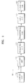
- FIG. 1 is a block diagram of an image forming apparatus which represents a typical apparatus in which a power supply apparatus according to an aspect of the present invention can be installed.
- the image forming apparatus may include a charging unit 110, an exposure unit 120, a developing unit 130, a transferring unit 140, a fixing unit 150, and a cleaning unit 160.
- the power supply apparatus receives an input voltage, and outputs one or more output voltages by using (or converting) the input voltage.
- the image forming apparatus is an apparatus having a print function (e.g., a printer and/or a multi function peripheral (MFP) having a print function).
- the image forming apparatus is assumed to be a laser beam printer (LBP) that performs single-color printing, for convenience of description.
- LBP laser beam printer
- other devices having plurality of components such as a personal computer may also be suitable for the embodiments of the present invention.
- the charging unit 110 regularly charges an entire surface of a photoconductive drum (not shown) installed in the image forming apparatus with a charge of a predetermined polarity. Then, the exposure unit 120 performs exposure with respect to the entire surface of the photoconductive drum according to print data input through an input terminal IN 1 so that an electrostatic latent image (not shown) is formed to correspond to the print data on the surface of the photoconductive drum.
- the electrostatic latent image has a predetermined polarity (e.g. positive (+)).
- the developing unit 130 develops the electrostatic latent image, which is formed on the surface of the photoconductive drum by the exposure unit 120, using a developer (e.g., toner) so that a developed image (not shown) is formed.
- the developer has a predetermined polarity (e.g., negative (-)).
- the transferring unit 140 transfers the developed image, which is formed on the surface of the photoconductive drum by the developing unit 130, onto a printing medium (not shown).
- the printing medium is a medium to be printed, and may be paper, an overhead projection (OHP) film, or the like.
- the fixing unit 150 fixes the developed image onto the printing medium, which is transferred onto the printing medium by the transferring unit 140. In particular, the fixing unit 150 fixes the developed image onto the printing medium using heat and pressure.
- the cleaning unit 160 operates after the operation of the transferring unit 140 is finished, and removes the developer left on the surface of the photoconductive drum. Ideally, all of the developer, by which the developed image is formed on the surface of the photoconductive drum, should be transferred onto the printing medium. However, a part of the developer can actually remain on the surface of the photoconductive drum even after the transferring operation is finished. After the operation of the transferring unit 140 is finished with respect to the print data input through an input terminal IN 1 for an nth time (where n is a natural number), the developer left on the surface of the photoconductive drum deteriorates the print quality of a printed matter with respect to the print data, which is input through the input terminal IN 1 at an n+1th time. Thus, prior to the operation of the exposure unit 120 with respect to the print data input for the n+1th time, the developer left on the surface of the photoconductive drum may be clearly removed by the cleaning unit 160.
- the charge unit 110, the exposure unit 120, the developing unit 130, the transferring unit 140, the fixing unit 150, and the cleaning unit 160 are components of the image forming apparatus.
- Each of the charging unit 110, the exposure unit 120, the developing unit 130, the transferring unit 140, the fixing unit 150, and the cleaning unit 160 are electronically operated using received power. In being electronically operated, the voltage of the power to be supplied to each of the charging unit 110, the exposure unit 120, the developing unit 130, the transferring unit 140, the fixing unit 150, and the cleaning unit 160 may be different from one another.
- FIG. 2 is a block diagram of a power supply apparatus according to an aspect of the present invention.
- the power supply apparatus includes an input terminal IN 2, a high voltage generating unit 210 (also referred to as a high voltage generator unit 210, or a voltage generator 210), and a plurality of output terminals OUT 1 through OUT N (where N is an integer and N ⁇ 2).
- the high voltage generating unit 210 generates one or more voltages (i.e., n voltages, where n is a natural number) using a voltage input through the input terminal IN 2, and outputs the generated voltages through the output terminals OUT 1 through OUT n.
- the high voltage generating unit 210 is implemented not as 'a plurality of circuit elements discretely distributed on a circuit board,' but rather, as 'a module disposed on a circuit board'.
- the high voltage generating unit 210 is implemented as 'a chip disposed on a circuit board'.
- the high voltage generating unit 210 includes a transforming unit 220 and a rectifying unit 230.
- the transforming unit 220 transforms a voltage input through the input terminal IN 2 into one or more output voltages (i.e. N voltages), which if more than one, is different from one another, though not required. In other embodiments, two or more output voltages may be the same.
- the rectifying unit 230 rectifies the n voltages output from the transforming unit 220, and outputs the rectified voltages through the output terminals OUT 1 through OUT N. That is, the rectifying unit 230 rectifies each of the n voltages output from the transforming unit 220, determines the n voltages as 'the n voltages generated by the high voltage generating unit 210' referred to above, and outputs the determined N voltages through the output terminals OUT 1 through OUT N as N output voltages. In various aspects, the respective output terminals OUT 1 through OUT N may respectively output the N output voltages.
- the input terminal IN 2, the high voltage generating unit 210, and the output terminals OUT1 through OUT N are all disposed on a same circuit board.
- the input terminal IN 2, the high voltage generating unit 210, and the output terminals OUT1 through OUT N are all disposed on a single platform, such as a chip or a module.
- the chip or the module may be a solid state device.
- the chip may be an integrated circuit, which may be based on a ceramic or a non-conducting substrate.
- the module may be a self-contained electronic device with one or more subcomponents.
- the plurality of electronic components may be directly connected to the output terminals OUT 1 through OUT N, or may be connected by wires thereto.
- FIG. 3 is a view illustrating a circuit board 300 implementing a typical power supply apparatus.
- the typical power supply apparatus is implemented on the circuit board 300. Accordingly, 'an input terminal (not shown)', 'a plurality of output terminals 310, 312, 314, and 316', and 'a plurality of circuit elements discretely distributed on the circuit board 300' are provided on the circuit board 300 that includes the typical power supply apparatus.
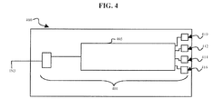
- FIG. 4 is a view illustrating a circuit board 400 on which a power supply apparatus 401 according to an aspect of the present invention is implemented.
- 'an input terminal IN 3', 'a plurality of output terminals 410, 412, 414, and 416' and 'a module 405 (e.g., a chip)' are provided on the circuit board 400, unlike the circuit board 300 of FIG. 3 .
- the module 405 may be the high voltage generating unit 210 of FIG. 2 .
- the number of output terminals may be any number.
- An area of the circuit board 300, on which the typical 'circuit elements discretely distributed on the circuit board 300' are occupied, would be wider than an area of the circuit board 400, on which the 'module 405' according to the present invention is occupied.
- a plurality of circuit elements are implemented as a module in the power supply apparatus according to aspects of the present invention, wherein the circuit elements generate one or more voltages using an input voltage.
- the circuit element is implemented as a module or a chip.
- the power supply apparatus can be miniaturized.
- an apparatus, in which the power supply apparatus is installed, can be miniaturized.
- the high voltage generating unit 210 may be a voltage multiplier that may be on a chip, or may be a power converter that converts AC power to DC power, or DC power to DC power, etc.
Landscapes
- Engineering & Computer Science (AREA)
- Power Engineering (AREA)
- Physics & Mathematics (AREA)
- General Physics & Mathematics (AREA)
- Microelectronics & Electronic Packaging (AREA)
- Dc-Dc Converters (AREA)
- Control Or Security For Electrophotography (AREA)
- Direct Current Feeding And Distribution (AREA)
- Electrophotography Configuration And Component (AREA)
Abstract
Description
- Aspects of the present invention relate to a power supply apparatus,.
- Power supplied to various electronic components of an electronic device can comprise direct current (DC) voltages that are different from one another. In this case, a power supply apparatus is provided in the electronic device, wherein the power supply apparatus generates the DC voltages to be supplied to the various electronic components by using an input voltage. The power supply apparatus includes various elements that receive the input voltage and generate the DC voltages different from one another by using the input voltage.
- In a typical power supply apparatus, as the number of output voltages that can be generated by using an input voltage increases, the power supply apparatus is implemented on a circuit board having an increasing number of circuit elements arranged therein. In the typical power supply apparatus, the larger the number of output voltages that can be generated, the greater the size of the typical power supply apparatus. Therefore, it is difficult to miniaturize an electronic device that uses DC voltages that are different from one another, and thus, it is difficult to satisfy a recent trend in which miniaturized products hold a high market share.
- According to an aspect of the present invention, a power supply apparatus includes a high voltage generating unit, which generates one or more output voltages by using an input voltage, and which is implemented as a chip; and one or more output terminals formed on a same circuit board as the high voltage generating unit, to output the generated one or more output voltages.
- According to another aspect of the present invention, a power supply apparatus includes: a high voltage generating unit, which generates one or more output voltages by using an input voltage, and which is implemented as a module; and one or more output terminals disposed on a same circuit board as the high voltage generating unit, to output the generated one or more output voltages.
- According to another aspect of the present invention, a power supply apparatus formed on a circuit board includes: a plurality of circuit components mounted on the circuit board; a solid-state electronic voltage converter mounted on the circuit board to convert an input voltage into one or more output voltages; and one or more output terminals mounted on the circuit board and corresponding to the one or more output voltages to output the one or more output voltages.
- According to another aspect of the present invention, a solid state power supply apparatus includes: an input terminal to receive an input voltage; a voltage converter to convert the input voltage into one or more output voltages; and one or more output terminals to output the one or more output voltages and each corresponding to the one or more output voltages.
- According to the present invention there is provided an apparatus and method as set forth in the appended claims. Other features of the invention will be apparent from the dependent claims, and the description which follows.
- For a better understanding of the invention, and to show how embodiments of the same may be carried into effect, reference will now be made, by way of example, to the accompanying diagrammatic drawings in which:
-
FIG. 1 is a block diagram of an image forming apparatus which represents a typical apparatus in which a power supply apparatus according to an aspect of the present invention can be installed; -
FIG. 2 is a block diagram of a power supply apparatus according to an aspect of the present invention; -
FIG. 3 is a view illustrating a circuit board implementing a typical power supply apparatus; and -
FIG. 4 is a view illustrating a circuit board on which a power supply apparatus according to an aspect of the present invention is implemented. -
FIG. 1 is a block diagram of an image forming apparatus which represents a typical apparatus in which a power supply apparatus according to an aspect of the present invention can be installed. The image forming apparatus may include acharging unit 110, anexposure unit 120, a developingunit 130, a transferringunit 140, afixing unit 150, and acleaning unit 160. - The power supply apparatus receives an input voltage, and outputs one or more output voltages by using (or converting) the input voltage. The image forming apparatus is an apparatus having a print function (e.g., a printer and/or a multi function peripheral (MFP) having a print function). Hereinafter, the image forming apparatus is assumed to be a laser beam printer (LBP) that performs single-color printing, for convenience of description. However, in other aspects, other devices having plurality of components such as a personal computer may also be suitable for the embodiments of the present invention.
- In reference to
FIG. 1 , thecharging unit 110 regularly charges an entire surface of a photoconductive drum (not shown) installed in the image forming apparatus with a charge of a predetermined polarity. Then, theexposure unit 120 performs exposure with respect to the entire surface of the photoconductive drum according to print data input through aninput terminal IN 1 so that an electrostatic latent image (not shown) is formed to correspond to the print data on the surface of the photoconductive drum. The electrostatic latent image has a predetermined polarity (e.g. positive (+)). - The developing
unit 130 develops the electrostatic latent image, which is formed on the surface of the photoconductive drum by theexposure unit 120, using a developer (e.g., toner) so that a developed image (not shown) is formed. The developer has a predetermined polarity (e.g., negative (-)). The transferringunit 140 transfers the developed image, which is formed on the surface of the photoconductive drum by the developingunit 130, onto a printing medium (not shown). The printing medium is a medium to be printed, and may be paper, an overhead projection (OHP) film, or the like. Thefixing unit 150 fixes the developed image onto the printing medium, which is transferred onto the printing medium by the transferringunit 140. In particular, thefixing unit 150 fixes the developed image onto the printing medium using heat and pressure. - The
cleaning unit 160 operates after the operation of the transferringunit 140 is finished, and removes the developer left on the surface of the photoconductive drum. Ideally, all of the developer, by which the developed image is formed on the surface of the photoconductive drum, should be transferred onto the printing medium. However, a part of the developer can actually remain on the surface of the photoconductive drum even after the transferring operation is finished. After the operation of the transferringunit 140 is finished with respect to the print data input through aninput terminal IN 1 for an nth time (where n is a natural number), the developer left on the surface of the photoconductive drum deteriorates the print quality of a printed matter with respect to the print data, which is input through theinput terminal IN 1 at an n+1th time. Thus, prior to the operation of theexposure unit 120 with respect to the print data input for the n+1th time, the developer left on the surface of the photoconductive drum may be clearly removed by thecleaning unit 160. - The
charge unit 110, theexposure unit 120, the developingunit 130, the transferringunit 140, thefixing unit 150, and thecleaning unit 160 are components of the image forming apparatus. Each of thecharging unit 110, theexposure unit 120, the developingunit 130, the transferringunit 140, thefixing unit 150, and thecleaning unit 160 are electronically operated using received power. In being electronically operated, the voltage of the power to be supplied to each of thecharging unit 110, theexposure unit 120, the developingunit 130, the transferringunit 140, thefixing unit 150, and thecleaning unit 160 may be different from one another. -
FIG. 2 is a block diagram of a power supply apparatus according to an aspect of the present invention. The power supply apparatus includes aninput terminal IN 2, a high voltage generating unit 210 (also referred to as a highvoltage generator unit 210, or a voltage generator 210), and a plurality ofoutput terminals OUT 1 through OUT N (where N is an integer and N≥ 2). - In reference to
FIG. 2 , the highvoltage generating unit 210 generates one or more voltages (i.e., n voltages, where n is a natural number) using a voltage input through theinput terminal IN 2, and outputs the generated voltages through theoutput terminals OUT 1 through OUT n. - The high
voltage generating unit 210 is implemented not as 'a plurality of circuit elements discretely distributed on a circuit board,' but rather, as 'a module disposed on a circuit board'. For example, the highvoltage generating unit 210 is implemented as 'a chip disposed on a circuit board'. - The high
voltage generating unit 210 includes a transformingunit 220 and a rectifyingunit 230. The transformingunit 220 transforms a voltage input through theinput terminal IN 2 into one or more output voltages (i.e. N voltages), which if more than one, is different from one another, though not required. In other embodiments, two or more output voltages may be the same. - The rectifying
unit 230 rectifies the n voltages output from the transformingunit 220, and outputs the rectified voltages through theoutput terminals OUT 1 through OUT N. That is, the rectifyingunit 230 rectifies each of the n voltages output from the transformingunit 220, determines the n voltages as 'the n voltages generated by the high voltage generating unit 210' referred to above, and outputs the determined N voltages through theoutput terminals OUT 1 through OUT N as N output voltages. In various aspects, the respectiveoutput terminals OUT 1 through OUT N may respectively output the N output voltages. - In an example embodiment of the present invention, the
input terminal IN 2, the highvoltage generating unit 210, and the output terminals OUT1 through OUT N are all disposed on a same circuit board. In other aspects, theinput terminal IN 2, the highvoltage generating unit 210, and the output terminals OUT1 through OUT N are all disposed on a single platform, such as a chip or a module. If disposed on a chip or a module, the chip or the module may be a solid state device. The chip may be an integrated circuit, which may be based on a ceramic or a non-conducting substrate. The module may be a self-contained electronic device with one or more subcomponents. - If the power supply apparatus according to the present invention is installed in the image forming apparatus as shown in
FIG. 1 , for example, at least one of the output terminals OUT N through OUT N (e.g., n=4), is connected to at least one of a plurality of electronic components (e.g., thecharging unit 110, theexposure unit 120, the developingunit 130, thetransferring unit 140, thefixing unit 150 and the cleaning unit 160) installed in the image forming apparatus. At this time, the plurality of electronic components may be directly connected to the output terminals OUT 1 through OUT N, or may be connected by wires thereto. -
FIG. 3 is a view illustrating acircuit board 300 implementing a typical power supply apparatus. Referring toFIG. 3 , the typical power supply apparatus is implemented on thecircuit board 300. Accordingly, 'an input terminal (not shown)', 'a plurality ofoutput terminals circuit board 300 that includes the typical power supply apparatus. -
FIG. 4 is a view illustrating acircuit board 400 on which apower supply apparatus 401 according to an aspect of the present invention is implemented. As shown, 'an input terminal IN 3', 'a plurality ofoutput terminals circuit board 400, unlike thecircuit board 300 ofFIG. 3 . In aspects of the present invention, themodule 405 may be the highvoltage generating unit 210 ofFIG. 2 . In aspects of the present invention, the number of output terminals may be any number. - An area of the
circuit board 300, on which the typical 'circuit elements discretely distributed on the circuit board 300' are occupied, would be wider than an area of thecircuit board 400, on which the 'module 405' according to the present invention is occupied. - As described above, a plurality of circuit elements are implemented as a module in the power supply apparatus according to aspects of the present invention, wherein the circuit elements generate one or more voltages using an input voltage. For example, the circuit element is implemented as a module or a chip. Thus, although the number of voltages, which can be generated by the power supply apparatus, is large, the power supply apparatus can be miniaturized. In addition, an apparatus, in which the power supply apparatus is installed, can be miniaturized.
- In various aspects, the high
voltage generating unit 210 may be a voltage multiplier that may be on a chip, or may be a power converter that converts AC power to DC power, or DC power to DC power, etc. - Although a few preferred embodiments have been shown and described, it will be appreciated by those skilled in the art that various changes and modifications might be made without departing from the scope of the invention, as defined in the appended claims.
- Attention is directed to all papers and documents which are filed concurrently with or previous to this specification in connection with this application and which are open to public inspection with this specification, and the contents of all such papers and documents are incorporated herein by reference.
- All of the features disclosed in this specification (including any accompanying claims, abstract and drawings), and/or all of the steps of any method or process so disclosed, may be combined in any combination, except combinations where at least some of such features and/or steps are mutually exclusive.
- Each feature disclosed in this specification (including any accompanying claims, abstract and drawings) may be replaced by alternative features serving the same, equivalent or similar purpose, unless expressly stated otherwise. Thus, unless expressly stated otherwise, each feature disclosed is one example only of a generic series of equivalent or similar features.
- The invention is not restricted to the details of the foregoing embodiment(s). The invention extends to any novel one, or any novel combination, of the features disclosed in this specification (including any accompanying claims, abstract and drawings), or to any novel one, or any novel combination, of the steps of any method or process so disclosed.
Claims (12)
- A power supply apparatus comprising:a high voltage generating unit (210), which generates one or more output voltages by using an input voltage, and which is implemented as a chip; andone or more output terminals (OUT 1,...,OUT N) formed on a same circuit board as the high voltage generating unit (210), to output the generated one or more output voltages.
- The apparatus of claim 1, wherein the chip comprises:a transforming unit (220) to transform the input voltage into one or more transformed voltages that are different from one another; anda rectifying unit (230) to rectify the transformed voltages into rectified voltages, and to determine the rectified voltages as the generated one or more output voltages.
- The apparatus of claim 1 or 2, wherein the power supply apparatus is installed in an image forming apparatus.
- The apparatus of claim 3, wherein the one or more output terminals are installed in the image forming apparatus, and each of the output terminals is connected to at least one of a plurality of electronic components of the image forming apparatus.
- A power supply apparatus comprising:a high voltage generating unit (210), which generates one or more output voltages by using an input voltage, and which is implemented as a module; andone or more output terminals (OUT 1,...,OUT N) disposed on a same circuit board as the high voltage generating unit, to output the generated one or more output voltages.
- The apparatus of claim 5, wherein the module comprises:a transforming unit (210) to transform the input voltage into one or more transformed voltages that are different from one another; anda rectifying unit (230) to rectify the transformed voltages, and to determine the rectified voltages as the generated one or more output voltages.
- The apparatus of claim 5 or 6, wherein the power supply apparatus is installed in an image forming apparatus.
- The apparatus of claim 7, wherein the one or more output terminals are installed in the image forming apparatus, and each of the output terminals is connected to at least one of a plurality of electronic components of the image forming apparatus.
- A power supply apparatus formed on a circuit board (400) comprising:a plurality of circuit components mounted on the circuit board;a solid-state electronic voltage converter mounted on the circuit board to convert an input voltage into one or more output voltages (405); andone or more output terminals (410,...,416) mounted on the circuit board and corresponding to the one or more output voltages to output the one or more output voltages.
- The apparatus of claim 9, wherein the solid-state electronic voltage converter comprises:a transformer (210) to transform the input voltage into one or more transformed voltages that are different from one another; anda rectifier (220) to rectify the transformed voltages into corresponding rectified voltages, and outputting the corresponding rectified voltages as the one or more output voltages, respectively.
- A solid state power supply apparatus comprising:an input terminal to receive an input voltage;a voltage converter to convert the input voltage into one or more output voltages; andone or more output terminals to output the one or more output voltages and each corresponding to the one or more output voltages.
- The apparatus of claim 11, wherein the voltage converter comprises:a transformer (210) to transform the input voltage into one or more transformed voltages that are different from one another; anda rectifier (220) to rectify the transformed voltages into corresponding rectified voltages, and outputting the corresponding rectified voltages as the one or more output voltages, respectively.
Applications Claiming Priority (1)
| Application Number | Priority Date | Filing Date | Title |
|---|---|---|---|
| KR20070070770 | 2007-07-13 |
Publications (2)
| Publication Number | Publication Date |
|---|---|
| EP2015432A2 true EP2015432A2 (en) | 2009-01-14 |
| EP2015432A3 EP2015432A3 (en) | 2016-11-16 |
Family
ID=39897597
Family Applications (1)
| Application Number | Title | Priority Date | Filing Date |
|---|---|---|---|
| EP08150707.1A Ceased EP2015432A3 (en) | 2007-07-13 | 2008-01-28 | Power supply apparatus |
Country Status (4)
| Country | Link |
|---|---|
| US (2) | US8274176B2 (en) |
| EP (1) | EP2015432A3 (en) |
| KR (1) | KR20090007248A (en) |
| CN (2) | CN101345486A (en) |
Families Citing this family (6)
| Publication number | Priority date | Publication date | Assignee | Title |
|---|---|---|---|---|
| US8274176B2 (en) * | 2007-07-13 | 2012-09-25 | Samsung Electronics Co., Ltd. | Power supply apparatus |
| JP5582055B2 (en) | 2011-02-14 | 2014-09-03 | ブラザー工業株式会社 | Image forming apparatus |
| RU2457601C1 (en) * | 2011-02-14 | 2012-07-27 | Федеральное государственное учреждение "33 Центральный научно-исследовательский испытательный институт" Министерства обороны Российской Федерации | Voltage converter |
| CN102508417B (en) * | 2011-11-16 | 2014-06-18 | 珠海天威飞马打印耗材有限公司 | Laser printer and modification method thereof |
| KR102079795B1 (en) * | 2013-07-19 | 2020-02-21 | 휴렛-팩커드 디벨롭먼트 컴퍼니, 엘.피. | Image forming apparatus and chip |
| CN115549262A (en) * | 2022-06-27 | 2022-12-30 | 宁德新能源科技有限公司 | Power module and electrical device |
Family Cites Families (20)
| Publication number | Priority date | Publication date | Assignee | Title |
|---|---|---|---|---|
| US4481566A (en) * | 1983-04-04 | 1984-11-06 | International Business Machines Corporation | On chip charge trap compensated high voltage converter |
| KR0150384B1 (en) | 1995-05-31 | 1998-10-15 | 배순훈 | High voltage stabilization circuit |
| US5815771A (en) | 1997-04-11 | 1998-09-29 | Xerox Corporation | Apparatus for applying a high voltage electrical point of load contact |
| US6420954B1 (en) * | 1999-12-10 | 2002-07-16 | Micron Technology, Inc. | Coupled multilayer soft magnetic films for high frequency microtransformer for system-on-chip power supply |
| JP2001256717A (en) | 2000-03-14 | 2001-09-21 | Matsushita Electric Ind Co Ltd | Disk unit |
| KR100387382B1 (en) | 2000-09-25 | 2003-06-19 | 박준호 | Switching mode power supply with high efficiency |
| JP4272851B2 (en) * | 2002-07-01 | 2009-06-03 | キヤノン株式会社 | Image forming apparatus |
| US6707367B2 (en) * | 2002-07-23 | 2004-03-16 | Broadcom, Corp. | On-chip multiple tap transformer and inductor |
| KR100497480B1 (en) | 2002-11-19 | 2005-07-01 | 삼성전자주식회사 | Color image forming machine |
| JP4353853B2 (en) * | 2004-05-20 | 2009-10-28 | 三洋電機株式会社 | Circuit device manufacturing method and plate-like body |
| KR100561429B1 (en) * | 2004-05-25 | 2006-03-17 | 삼성전자주식회사 | Developer's Voltage Supply |
| KR100601716B1 (en) * | 2005-01-05 | 2006-07-18 | 삼성전자주식회사 | High pressure generator and roll resistance sensing method |
| KR100636222B1 (en) | 2005-02-02 | 2006-10-19 | 삼성전자주식회사 | ASICized analog controller of high-voltage power supply (HPPS) for image forming apparatus |
| KR100787231B1 (en) * | 2005-04-23 | 2007-12-21 | 삼성전자주식회사 | High voltage generator, high voltage generator and ASIC chip |
| KR100708480B1 (en) | 2005-10-20 | 2007-04-18 | 삼성전자주식회사 | High voltage power supply and its high voltage power control method |
| US7369419B2 (en) * | 2006-07-05 | 2008-05-06 | Vanguard International Semiconductor Corporation | Voltage converter |
| US20080231115A1 (en) * | 2007-03-16 | 2008-09-25 | Gyuha Cho | Multiple-Output DC-DC Converter |
| US7932640B2 (en) * | 2007-06-07 | 2011-04-26 | Samsung Electronics Co., Ltd. | High voltage power supply |
| US8274176B2 (en) * | 2007-07-13 | 2012-09-25 | Samsung Electronics Co., Ltd. | Power supply apparatus |
| KR101238373B1 (en) | 2008-07-24 | 2013-02-28 | 삼성전자주식회사 | Apparatus for supplying high voltage power |
-
2007
- 2007-12-21 US US11/962,447 patent/US8274176B2/en not_active Expired - Fee Related
-
2008
- 2008-01-28 EP EP08150707.1A patent/EP2015432A3/en not_active Ceased
- 2008-02-04 CN CNA2008100054631A patent/CN101345486A/en active Pending
- 2008-02-04 CN CN201410569415.0A patent/CN104319990A/en active Pending
- 2008-07-14 KR KR1020080068349A patent/KR20090007248A/en not_active Ceased
-
2012
- 2012-07-09 US US13/544,300 patent/US8487475B2/en not_active Expired - Fee Related
Non-Patent Citations (1)
| Title |
|---|
| None * |
Also Published As
| Publication number | Publication date |
|---|---|
| US20090015062A1 (en) | 2009-01-15 |
| CN104319990A (en) | 2015-01-28 |
| CN101345486A (en) | 2009-01-14 |
| US8274176B2 (en) | 2012-09-25 |
| EP2015432A3 (en) | 2016-11-16 |
| US8487475B2 (en) | 2013-07-16 |
| KR20090007248A (en) | 2009-01-16 |
| US20130016990A1 (en) | 2013-01-17 |
Similar Documents
| Publication | Publication Date | Title |
|---|---|---|
| US8487475B2 (en) | Power supply apparatus and method of supplying power | |
| KR101571336B1 (en) | High Voltage Power Supply for image forming apparatus | |
| CN101546960B (en) | Power source apparatus | |
| US8269473B2 (en) | AC high voltage power supply device, charging device, developing device, and image forming apparatus | |
| JP2020160245A (en) | Power control device and image formation apparatus | |
| KR101238372B1 (en) | Apparatus for supplying high voltage power | |
| JP5880023B2 (en) | Power supply circuit, image forming apparatus | |
| JP7516875B2 (en) | Image forming device | |
| US8260167B2 (en) | High-voltage power supply | |
| JP5784055B2 (en) | Image forming apparatus and circuit board | |
| US8350407B2 (en) | High voltage power supply apparatus | |
| US20200192269A1 (en) | Image forming apparatus | |
| JP2012055141A (en) | Ac power supply device, charging device, and image forming device | |
| US20080050143A1 (en) | Shared High Voltage Power Supply for Photoconductor Charging in an Electrophotographic Device | |
| JP2021069254A (en) | Power supply device and image forming apparatus | |
| JP7180437B2 (en) | Image forming apparatus and discharge control method | |
| US10359725B2 (en) | Power source device and image forming apparatus | |
| JP5297760B2 (en) | Integrated circuit, circuit board including the integrated circuit, and image forming apparatus | |
| EP1736834A1 (en) | High Voltage Power Supply and Digital Control Method Thereof | |
| JP2006154077A (en) | High voltage power supply | |
| JP2010139900A (en) | Power source device, and image forming apparatus provided therewith | |
| JP2016067103A (en) | Power supply circuit and image forming apparatus | |
| JP2001060024A (en) | Composite high voltage power supply board | |
| JP2020118915A (en) | Image forming apparatus, paper separation method, and paper separation control program | |
| JP2001194958A (en) | Image forming device |
Legal Events
| Date | Code | Title | Description |
|---|---|---|---|
| PUAI | Public reference made under article 153(3) epc to a published international application that has entered the european phase |
Free format text: ORIGINAL CODE: 0009012 |
|
| AK | Designated contracting states |
Kind code of ref document: A2 Designated state(s): AT BE BG CH CY CZ DE DK EE ES FI FR GB GR HR HU IE IS IT LI LT LU LV MC MT NL NO PL PT RO SE SI SK TR |
|
| AX | Request for extension of the european patent |
Extension state: AL BA MK RS |
|
| RAP1 | Party data changed (applicant data changed or rights of an application transferred) |
Owner name: SAMSUNG ELECTRONICS CO., LTD. |
|
| PUAL | Search report despatched |
Free format text: ORIGINAL CODE: 0009013 |
|
| RIC1 | Information provided on ipc code assigned before grant |
Ipc: H02M 3/335 20060101ALI20160919BHEP Ipc: H02M 3/00 20060101AFI20160919BHEP |
|
| AK | Designated contracting states |
Kind code of ref document: A3 Designated state(s): AT BE BG CH CY CZ DE DK EE ES FI FR GB GR HR HU IE IS IT LI LT LU LV MC MT NL NO PL PT RO SE SI SK TR |
|
| AX | Request for extension of the european patent |
Extension state: AL BA MK RS |
|
| RIC1 | Information provided on ipc code assigned before grant |
Ipc: H02M 3/00 20060101AFI20161010BHEP Ipc: H02M 3/335 20060101ALI20161010BHEP |
|
| STAA | Information on the status of an ep patent application or granted ep patent |
Free format text: STATUS: REQUEST FOR EXAMINATION WAS MADE |
|
| 17P | Request for examination filed |
Effective date: 20170214 |
|
| RAP1 | Party data changed (applicant data changed or rights of an application transferred) |
Owner name: S-PRINTING SOLUTION CO., LTD. |
|
| RBV | Designated contracting states (corrected) |
Designated state(s): AT BE BG CH CY CZ DE DK EE ES FI FR GB GR HR HU IE IS IT LI LT LU LV MC MT NL NO PL PT RO SE SI SK TR |
|
| STAA | Information on the status of an ep patent application or granted ep patent |
Free format text: STATUS: EXAMINATION IS IN PROGRESS |
|
| RBV | Designated contracting states (corrected) |
Designated state(s): AT BE BG CH CY CZ DE DK EE ES FI FR GB GR HR HU IE IS IT LI LT LU LV MC MT NL NO PL PT RO SE SI SK TR |
|
| 17Q | First examination report despatched |
Effective date: 20170331 |
|
| AKX | Designation fees paid |
Designated state(s): AT BE BG CH CY CZ DE DK EE ES FI FR GB GR HR HU IE IS IT LI LT LU LV MC MT NL NO PL PT RO SE SI SK TR |
|
| AXX | Extension fees paid |
Extension state: RS Extension state: BA Extension state: MK Extension state: AL |
|
| RAP1 | Party data changed (applicant data changed or rights of an application transferred) |
Owner name: HP PRINTING KOREA CO., LTD. |
|
| STAA | Information on the status of an ep patent application or granted ep patent |
Free format text: STATUS: THE APPLICATION HAS BEEN REFUSED |
|
| 18R | Application refused |
Effective date: 20190210 |