EP2015402B1 - Electric connector - Google Patents
Electric connector Download PDFInfo
- Publication number
- EP2015402B1 EP2015402B1 EP08252372.1A EP08252372A EP2015402B1 EP 2015402 B1 EP2015402 B1 EP 2015402B1 EP 08252372 A EP08252372 A EP 08252372A EP 2015402 B1 EP2015402 B1 EP 2015402B1
- Authority
- EP
- European Patent Office
- Prior art keywords
- contacts
- contact
- main portion
- electric connector
- lead
- Prior art date
- Legal status (The legal status is an assumption and is not a legal conclusion. Google has not performed a legal analysis and makes no representation as to the accuracy of the status listed.)
- Active
Links
- 238000003780 insertion Methods 0.000 description 28
- 230000037431 insertion Effects 0.000 description 28
- 230000005540 biological transmission Effects 0.000 description 8
- 230000011664 signaling Effects 0.000 description 7
- 239000004734 Polyphenylene sulfide Substances 0.000 description 2
- 239000000470 constituent Substances 0.000 description 2
- 229920001707 polybutylene terephthalate Polymers 0.000 description 2
- 229920000069 polyphenylene sulfide Polymers 0.000 description 2
- 230000008878 coupling Effects 0.000 description 1
- 238000010168 coupling process Methods 0.000 description 1
- 238000005859 coupling reaction Methods 0.000 description 1
- 230000000593 degrading effect Effects 0.000 description 1
- 238000001746 injection moulding Methods 0.000 description 1
- 238000004519 manufacturing process Methods 0.000 description 1
- 239000000463 material Substances 0.000 description 1
- 239000002184 metal Substances 0.000 description 1
- 230000002093 peripheral effect Effects 0.000 description 1
- -1 polybutylene terephthalate Polymers 0.000 description 1
- 230000008054 signal transmission Effects 0.000 description 1
- 239000007787 solid Substances 0.000 description 1
- 229920003002 synthetic resin Polymers 0.000 description 1
- 239000000057 synthetic resin Substances 0.000 description 1
Images


Classifications
-
- H—ELECTRICITY
- H01—ELECTRIC ELEMENTS
- H01R—ELECTRICALLY-CONDUCTIVE CONNECTIONS; STRUCTURAL ASSOCIATIONS OF A PLURALITY OF MUTUALLY-INSULATED ELECTRICAL CONNECTING ELEMENTS; COUPLING DEVICES; CURRENT COLLECTORS
- H01R12/00—Structural associations of a plurality of mutually-insulated electrical connecting elements, specially adapted for printed circuits, e.g. printed circuit boards [PCB], flat or ribbon cables, or like generally planar structures, e.g. terminal strips, terminal blocks; Coupling devices specially adapted for printed circuits, flat or ribbon cables, or like generally planar structures; Terminals specially adapted for contact with, or insertion into, printed circuits, flat or ribbon cables, or like generally planar structures
- H01R12/50—Fixed connections
- H01R12/51—Fixed connections for rigid printed circuits or like structures
-
- H—ELECTRICITY
- H01—ELECTRIC ELEMENTS
- H01R—ELECTRICALLY-CONDUCTIVE CONNECTIONS; STRUCTURAL ASSOCIATIONS OF A PLURALITY OF MUTUALLY-INSULATED ELECTRICAL CONNECTING ELEMENTS; COUPLING DEVICES; CURRENT COLLECTORS
- H01R13/00—Details of coupling devices of the kinds covered by groups H01R12/70 or H01R24/00 - H01R33/00
- H01R13/646—Details of coupling devices of the kinds covered by groups H01R12/70 or H01R24/00 - H01R33/00 specially adapted for high-frequency, e.g. structures providing an impedance match or phase match
- H01R13/6473—Impedance matching
- H01R13/6474—Impedance matching by variation of conductive properties, e.g. by dimension variations
-
- H—ELECTRICITY
- H01—ELECTRIC ELEMENTS
- H01R—ELECTRICALLY-CONDUCTIVE CONNECTIONS; STRUCTURAL ASSOCIATIONS OF A PLURALITY OF MUTUALLY-INSULATED ELECTRICAL CONNECTING ELEMENTS; COUPLING DEVICES; CURRENT COLLECTORS
- H01R12/00—Structural associations of a plurality of mutually-insulated electrical connecting elements, specially adapted for printed circuits, e.g. printed circuit boards [PCB], flat or ribbon cables, or like generally planar structures, e.g. terminal strips, terminal blocks; Coupling devices specially adapted for printed circuits, flat or ribbon cables, or like generally planar structures; Terminals specially adapted for contact with, or insertion into, printed circuits, flat or ribbon cables, or like generally planar structures
- H01R12/70—Coupling devices
- H01R12/71—Coupling devices for rigid printing circuits or like structures
- H01R12/712—Coupling devices for rigid printing circuits or like structures co-operating with the surface of the printed circuit or with a coupling device exclusively provided on the surface of the printed circuit
-
- H—ELECTRICITY
- H01—ELECTRIC ELEMENTS
- H01R—ELECTRICALLY-CONDUCTIVE CONNECTIONS; STRUCTURAL ASSOCIATIONS OF A PLURALITY OF MUTUALLY-INSULATED ELECTRICAL CONNECTING ELEMENTS; COUPLING DEVICES; CURRENT COLLECTORS
- H01R13/00—Details of coupling devices of the kinds covered by groups H01R12/70 or H01R24/00 - H01R33/00
- H01R13/646—Details of coupling devices of the kinds covered by groups H01R12/70 or H01R24/00 - H01R33/00 specially adapted for high-frequency, e.g. structures providing an impedance match or phase match
- H01R13/6473—Impedance matching
-
- Y—GENERAL TAGGING OF NEW TECHNOLOGICAL DEVELOPMENTS; GENERAL TAGGING OF CROSS-SECTIONAL TECHNOLOGIES SPANNING OVER SEVERAL SECTIONS OF THE IPC; TECHNICAL SUBJECTS COVERED BY FORMER USPC CROSS-REFERENCE ART COLLECTIONS [XRACs] AND DIGESTS
- Y10—TECHNICAL SUBJECTS COVERED BY FORMER USPC
- Y10S—TECHNICAL SUBJECTS COVERED BY FORMER USPC CROSS-REFERENCE ART COLLECTIONS [XRACs] AND DIGESTS
- Y10S439/00—Electrical connectors
- Y10S439/941—Crosstalk suppression
Definitions
- the present invention relates to an electric connector used mainly for high-speed digital signaling and capable of providing good impedance matches.
- an insulative body has groups of contacts disposed in two rows along its width, and the groups of contacts are arranged in a staggered or zigzag manner.
- the groups of contacts include ground contacts and pairs of signal contacts to serve as differential pairs for high-speed digital signaling.
- ground contacts are wider than some of the signal contacts making up a pair, and each of the ground contacts is arranged so that their widthwise ends overlap widthwise ends of each pair of signal contacts in plain positions.
- impedance is matched within each differential pair of contacts and among the differential pairs of contacts (see Japanese Published Patent Publication No. 2003-505826 (Translation of Published International Application No. WO01/006602 )).
- the present invention was made in view of the above circumstances, and an embodiment of the present invention provides an electric connector capable of providing good impedance matches without adding a dummy ground contact or changing the shape of the shield cover.
- WO 03/026078 Al discloses a connector with controlled impedance according to the preamble of claim 1.
- the connector includes at least one set of differential signal terminals with an associated ground terminal.
- the ground terminal has a symmetric configuration, while the two differential signal terminals have asymmetric configurations.
- the asymmetric configurations permit capacitive coupling to occur primarily between the two differential signals in an area of the connector where the inductance of the connector would be high.
- the two differential signal terminals flank the ground terminal.
- the invention provides an electric connector as defined in claim 1.
- one of the two contacts subject to impedance tuning has a width and an area thereof adjusted in accordance with a difference in impedance from impedances between other first and second contacts, impedance can be matched between the first and second contacts without adding a dummy ground contact or changing the shape of the shield cover; therefore, transmission characteristics of the connector can be improved without increase in costs.
- One of the first and second contacts present at the outermost end has its width and area adjusted to compensate for any difference in impedance from impedances between other first and second contacts.
- the groups of contacts may be arranged such that a plurality of sets is disposed in the lateral direction of the body with respective vertical positional relationships of the sets turned upside down alternately.
- Each of the sets may be made up by a pair of first contacts and a second contact, and the first contacts may be signal contacts and the second contact may be a ground contact.
- the pair of first contacts opposes the second contact within each set, while the pair of first contacts is positioned next to second contacts from other sets.
- This contact arrangement is advantageous in terms of impedance matching and reduction in crosstalk within each pair of first contacts.
- widthwise ends of the second contact are so positioned as to overlap widthwise inner ends of the pair of first contacts in plain position. That is to say, when viewed from below, and disregarding the material of the projecting portion of the connector body positioned between the upper and lower groups of contacts, the widthwise ends or edges of the lower contact overlap or overlie the widthwise inner ends of edges of the upper contact in each set. Conversely, when viewed from above, the upper contacts overlap or overlie the lower contacts at the edges. This arrangement is advantageous in terms of impedance matching within each pair of first contacts.
- impedance can be matched within the pair of first contacts at the outermost end without adding a dummy ground contact or changing the shape of the shield cover.
- the electric connector shown in FIGS. 1 to 3 is a receptacle adapted to be mounted to a circuit board, capable of high-speed differential signaling.
- the electric connector includes an insulative body 100, upper and lower groups of contacts 200a and 200b, and a shield cover 300 covering the outer periphery of the body 100.
- the upper and lower groups of contacts 200a and 200b are disposed in spaced relationship inside the body and arranged in two rows in a lateral direction of the body 100 in a staggered or zigzag manner.
- Each of the components of the electric connector is detailed in the following description.
- first or upper contacts and their features have an “a” suffix
- second or lower contacts and their features have a “b” suffix
- sets of first (upper) and second (lower) terminal insertion holes provided in the electrical connector are denoted by 111a and 111b, respectively.
- the body 100 is formed from a synthetic resin for general use such as PBT (polybutylene terephthalate) or PPS (polyphenylene sulfide) by injection molding.
- the body 100 can be mated with a plug A, shown in dotted outine in FIG. 5 .
- the body 100 includes a connector main portion 110 having a substantially rectangular solid shape, a projecting portion 120 having a substantially inverted-U shape as viewed from the front, a base 130 having a substantially plate-like shape, and a cylindrical boss 140.
- the projecting portion 120 is provided at the front side of the connector main portion 110 and adapted to enter into a recess provided at a tip end of the plug A.
- the base 130 is provided under the connector main portion 110 and extended forward.
- the boss 140 is formed downward on a bottom surface of the base 130 and fits into a hole (not shown) in the circuit board.
- terminal insertion holes 111a and 111b are lined at equal pitch intervals in the lateral direction of the electric connector in two rows. These holes in two rows are shifted in phase from one another with spacing in between, so as to correspond to contacts (not shown) of the plug A. As shown in FIG. 1 , the widthwise ends of the first terminal insertion holes 111a are located in such plan positions as to overlap the widthwise ends of the second terminal insertion holes 111b.
- the terminal insertion holes 111a and 111b are through holes of horizontally elongated rectangular shape. Ten such holes are provided in each of the upper and lower rows to correspond to contact main portions 2012a and 2022b of the upper and lower groups of contacts 200a and 200b. Of the twenty terminal insertion holes, all holes other than a terminal insertion hole 111b' at the rightmost end in the lower row in FIG. 1 are identical to one another.
- the terminal insertion hole 111b' at the rightmost end is a through hole of a horizontally elongated rectangular shape, is wider than the other terminal insertion holes 111a and 111b, and corresponds to a main portion 2012b in the lower group of contacts 200b.
- an apostrophe is added to the reference numeral as above for distinction from the other terminal insertion holes 111b.
- a cutout 112 is provided in the rear surface of the connector main portion 110.
- the terminal insertion grooves 113 are long grooves arranged in the lateral direction of the body.
- the terminal insertion grooves 113 correspond in lateral width to lead-out portions 2013a and 2013b of the upper and lower groups of contacts 200a and 200b.
- terminal guide grooves 121a communicating with the terminal insertion holes 111a in the connector main portion 110 and extending in straight lines in a longitudinal direction of the body 100.
- terminal guide grooves 121b communicating with the terminal insertion holes 111b in the main portion 110 and extending in straight lines in a longitudinal direction of the body 100.
- the terminal guide grooves 121a and 121b correspond in lateral width to contact portions 2011a and 2011b of the upper and lower groups of contacts 200a and 200b.
- the terminal guide grooves 121a and 121b are shifted from each other in phase in the lateral direction, in a similar manner to the terminal insertion holes 111a and 111b.
- the shield cover 300 is a metal shell which can be brought into contact with an outer peripheral shield (not shown) of the plug A as mated with the body 100.
- the shield cover 300 includes a cover main body 310, a pair of legs 320 extending downward from opposite widthwise ends of the cover body 310, and a back cover 330 for openably covering an opening on the back side of the cover body 310.
- the cover body 310 shaped as a substantially square cylinder, fits about the connector main portion 110 of the body 100 so as to cover four sides - upper, lower, right and left sides - of the connector main portion 110 and the projecting portion 120 (i.e., the outer peripheries of the connector main portion 110 and the projecting portion 120).
- the legs 320 are adapted to be inserted into attachment holes (not shown) in the circuit board and connected to a ground pattern on the circuit board.
- the back cover 330 is a plate-like member that has its upper end pivotably attached to an upper edge of the opening on the rear side of the cover main body 310.
- the back cover 330 closes the opening on the rear side of the cover main body 310 so as to cover the rear side of the connector main portion 110 of the body 100.
- the upper contact group 200a consists of contacts 201a-210a.
- the lower contact group 200b consists of contacts 201b-210b.
- the contact 201a is representative of the contacts in the upper contact group 200a and includes a contact portion 2011a, a contact main portion 2012a, a lead-out portion 2013a, and a lead portion 2014a.
- the contact portion 2011a is a plate-like portion that can be brought into contact with a contact (not shown) of the plug A as engaged with the projecting portion 120 of the body 100.
- the contact main portion 2012a a plate-like portion with a larger width than that of the contact portion 2011a, is provided continuously from or integral with the rear end of the contact portion 2011a and is adapted to be press fitted into the associated terminal insertion hole 111a in the body 100.
- the lead-out portion 2013a a rod-like portion provided continuously from or integral with the rear end of the contact main portion 2012a, is bent substantially at a right angle so as to extend along the rear surface of the body 100.
- the lead portion 2014a a rod-like portion provided continuously from or integral with the rear end of the lead-out portion 2013a, is bent substantially at a right angle so as to be connected to a pattern on the circuit board.
- the contact 202b is one of the contacts in the lower contact group 200b and includes a contact portion 2021b, a contact main portion 2022b, a lead-out portion 2023b, and a lead portion 2024b.
- the contact portion 2021b is a plate-like portion which can be brought into contact with a contact (not shown) of the plug A as engaged with the projecting portion 120 of the body 100.
- the contact main portion 2022b, a plate-like portion with a larger width than that of the contact portion 2021b, is provided continuously from or integral with the rear end of the contact portion 2021b and is adapted to be press fitted into the associated terminal insertion hole 111b in the body 100.
- the lead-out portion 2023b a rod-like portion provided continuously from or integral with the rear end of the contact main portion 2022b, is bent substantially at a right angle so as to extend along the rear surface of the body 100.
- the lead portion 2024b a rod-like portion provided continuously from or integral with the rear end of the lead-out portion 2023b, is bent substantially at a right angle so as to be connected to the pattern on the circuit board.
- the contacts of the upper group 200a such as contact 201a and the contacts of the lower group 200b such as contact 202b are different from each other in that the lead-out portion 2013a is longer than the respective lead-out portion 2023b by the length of distance between the upper row and the lower row.
- Contacts 202a, 204a, 205a, 208a and 209a are the same as the contact 201a.
- contacts 203a, 206a, 207a and 210a are the same as the contact 201a except that their contact portions 2031a, 2061a, 2071a and 2101a are each longer than the contact portion 2011a of the contact 201a.
- Contacts 203b, 205b, 206b and 209b are the same as the contact 202b.
- Contacts 204b, 207b, 208b and 210b are the same as the contact 202b except that their contact portions 2041b, 2071b, 2081b and 2101b are each longer than the contact portion 2021b of the contact 202b.
- a contact 201b is the same as the contact 202b, except that its contact portion 2011b is longer than the contact portion 2021b of the contact 202b and that it has a plate-like extended portion 2012b1 along a widthwise end of the main portion 2012b.
- the electric connector according to the present embodiment is used as a power source line and also used for transmission of single end signals and first to fifth differential signals.
- the contacts 207a, 210a, 207b, 209b and 210b are connected to a pattern on the circuit board to function as contacts used in a power supply line or for single-ended signaling.
- the contacts 201a, 202b, 204a, 205b and 208a function as positive signal contacts (i.e., one of first contacts in each pair) for transmission of the first to fifth differential signals
- the contacts 202a, 203b, 205a, 206b and 209a function as negative signal contacts (i.e., the other one of the first contacts in each pair) for transmission of the first to fifth differential signals
- the contacts 201b, 203a, 204b, 206a, and 208b function as common ground contacts (i.e., second contacts) for transmission of the first to fifth differential signals, respectively.
- each triangular set or group of three contacts is formed by one positive signal contact and one negative signal contact disposed at one side of the triangular arrangement and one common ground contact disposed at the opposite apex.
- These five sets are sequentially arranged in the lateral direction of the body 100 with their vertical orientations alternately inverted.
- the contacts for signal transmission and other use are arranged in the above-described relationship. Therefore, for the purpose of reducing a skew, etc. between adjacent contacts of each differential pair and between the differential pairs, the longitudinal relationship among the contact portions 2011a-2111a of the contacts 201a-210a and the contact portions 2011b-2111b of the contacts 201b-210b is established as shown in FIGS. 6A and 6B .
- the contacts 201a-210a are positioned and inserted into ten associated terminal insertion holes 111a in the body 100 from the rear side of the body 100. Then, the contact portions 2011a-2101a of the contacts 201a-210a are received in the respective ten terminal guide grooves 121a in the body 100. Simultaneously therewith, the contact main portions 2012a-2102a of the contacts 201a-210a are press fitted within the respective ten terminal insertion holes 111a, and the lead-out portions 2013a-2103a are received in the respective ten terminal insertion grooves 113.
- the contacts 201b-210b are positioned and inserted into the terminal insertion hole 111b' and the nine terminal insertion holes 111b in the body 100, respectively, from the rear side of the body 100. Then, the contact portions 2011b-2101b of the contacts 201b-210b are received in the respective ten terminal guide grooves 121b in the body 100. Simultaneously therewith, the contact main portions 2012b-2102b of the contacts 201b-210b are press fitted within the terminal insertion hole 111b' and the nine terminal insertion holes 111b, respectively, and the lead-out portions 2013b to 2103b are received in the remaining ten terminal insertion grooves 113.
- the widthwise ends of the contact main portions 2012a-2102a of the contacts 201a-210a are located in such plain positions as to overlap the widthwise ends of the contact main portions 2012b-2102b of the contacts 201b-210b.
- any one of the common ground contacts opposite widthwise ends of the contact main portion are located in such plain positions as to overlap an inner widthwise end of the contact main portion of the adjacent plus signal contact and an inner widthwise end of the contact main portion of the minus signal contact.
- the common ground contacts in other sets are arranged adjacent to these plus signal contacts and minus signal contacts. This arrangement of the contacts achieves excellently matched impedances in the respective differential pairs of contacts.
- the overlapping width and area (N1) of the extended portion 2012b1 of the contact main portion 2012b of the contact 201b overlapping the contact main portion 2012a of the contact 201a is approximately twice as large as each overlapping width and area (N2) of the ends of contact main portions of any other two contacts for differential signaling (i.e., the outer end and the inner end in each triangular set-for example, an end of the contact main portion 2032a of the contact 203a and an end of the contact main portion 2022b of the contact 202b that are next to each other).
- adjustment is made to the width and area of the contact main portion 2012b of the contact 201b, in accordance with the difference in impedance from other signal contacts with respect to common ground contacts.
- This structure prevents reduction in capacitance between the contact 201a and the contact 201b that should have been created due to the location of the contact 201a at the outmost end of the upper group of contacts 200a and absence of a neighboring common ground contact. Consequently, it becomes possible to suppress variation in impedance within the differential pair located at the outmost end of the groups of contacts, providing matched impedances.
- impedance can be matched within the differential pair at an outmost end of the groups of contacts without adding a dummy ground contact or changing the shape of the shield cover 300 as has been previously described. Matched impedances within each pair should result in matched impedances among the differential pairs. Accordingly, the transmission characteristics of the electric connector can be improved without increase in costs.
- any change in design can be made to the above-described electric connector as long as it includes an insulative body and groups of contacts disposed in spaced relationship inside the body, the contacts being arranged in at least two rows in a lateral direction of the body, as long as the groups of contacts include a plurality of first contacts; and a plurality of second contacts located in a different row from a row where their associated first contacts exist, the second contacts being arranged next to the first contacts, and as long as, out of one of the first contacts and one of the second contacts subject to impedance tuning, one of these two contacts has a width and an area thereof adjusted in accordance with a difference in impedance from impedances between other first and second contacts.
- the present invention is not limited thereto.
- the width and area of the main portion 2012a of the contact 201a which is a signal contact, may be reduced as compared with other signal contacts, thereby preventing reduction in capacitance between the contacts 201a and 201b to match the impedances.
- the contacts subject to impedance tuning are the contacts 201a, 202a, and 201b that are the differential pair and the common ground contact thereof at the outermost end in the groups of contacts, the present invention is not limited thereto. That is, contacts subject to impedance tuning may be appropriately selected depending on the arrangement of the contacts.
- the present electric connector can be applied to an electric connector for unbalanced (single-ended) signaling. More particularly, adjustment may be made to a single-ended signal contact and a ground contact thereof subject to impedance tuning, by adjusting a width and area of one of these two contacts in accordance with the difference in impedance from another set of a single-ended signal contact and a ground contact.
- the geometry of the contacts is not limited to one described in the above-described embodiment, and any change in design can be made.
- the arrangement design of the contacts can be changed as appropriate, so long as the contacts are arranged with spacing in at least two rows in the lateral direction inside the body.
- the present electric connector is an electric connector for differential signaling
- the contact arrangement may be modified such that, for example, a plurality of positive and negative signal contacts is arranged in a first row, and a plurality of common ground contacts is arranged in a second row.
- the contacts can also be arranged such that their widthwise ends do not overlap one another in their plain positions.
- the above electric connector is described as a receptacle, it may alternatively be a plug having contacts connected to a cable.
Landscapes
- Details Of Connecting Devices For Male And Female Coupling (AREA)
Description
- The present invention relates to an electric connector used mainly for high-speed digital signaling and capable of providing good impedance matches.
- In a known electric connector of this type, an insulative body has groups of contacts disposed in two rows along its width, and the groups of contacts are arranged in a staggered or zigzag manner. The groups of contacts include ground contacts and pairs of signal contacts to serve as differential pairs for high-speed digital signaling.
- Some of the ground contacts are wider than some of the signal contacts making up a pair, and each of the ground contacts is arranged so that their widthwise ends overlap widthwise ends of each pair of signal contacts in plain positions. With this structure, impedance is matched within each differential pair of contacts and among the differential pairs of contacts (see Japanese Published Patent Publication No.
2003-505826 WO01/006602 - However, as to a differential pair located at an outermost end of the groups of contacts, there is no ground contact disposed at one side of a signal contact of the differential pair. Therefore, capacitance of this signal contact with respect to a ground contact is smaller as compared with that of the other signal contact of the same differential pair, with the result of increased impedance. For this reason, there are impedance mismatches between the contacts, thereby degrading transmission characteristics of the connector.
- In this case, it is not impossible to improve impedance matching by disposing a dummy ground contact at the side of the signal contact in question or by bringing a portion of a shield cover of the electric connector close to the signal contact. However, the addition of a dummy ground contact or the change in shape of the shield cover will cause increase in the number of components and assembly steps, leading to increased costs.
- The present invention was made in view of the above circumstances, and an embodiment of the present invention provides an electric connector capable of providing good impedance matches without adding a dummy ground contact or changing the shape of the shield cover.
- Published international patent application No.
WO 03/026078 Al - In order to overcome the above problems, the invention provides an electric connector as defined in claim 1.
- With such an electric connector, since one of the two contacts subject to impedance tuning has a width and an area thereof adjusted in accordance with a difference in impedance from impedances between other first and second contacts, impedance can be matched between the first and second contacts without adding a dummy ground contact or changing the shape of the shield cover; therefore, transmission characteristics of the connector can be improved without increase in costs.
- One of the first and second contacts present at the outermost end has its width and area adjusted to compensate for any difference in impedance from impedances between other first and second contacts.
- The groups of contacts may be arranged such that a plurality of sets is disposed in the lateral direction of the body with respective vertical positional relationships of the sets turned upside down alternately. Each of the sets may be made up by a pair of first contacts and a second contact, and the first contacts may be signal contacts and the second contact may be a ground contact. In this case, the pair of first contacts opposes the second contact within each set, while the pair of first contacts is positioned next to second contacts from other sets. This contact arrangement is advantageous in terms of impedance matching and reduction in crosstalk within each pair of first contacts.
- It is preferred that in each of the sets, widthwise ends of the second contact are so positioned as to overlap widthwise inner ends of the pair of first contacts in plain position. That is to say, when viewed from below, and disregarding the material of the projecting portion of the connector body positioned between the upper and lower groups of contacts, the widthwise ends or edges of the lower contact overlap or overlie the widthwise inner ends of edges of the upper contact in each set. Conversely, when viewed from above, the upper contacts overlap or overlie the lower contacts at the edges. This arrangement is advantageous in terms of impedance matching within each pair of first contacts.
- In this case also, impedance can be matched within the pair of first contacts at the outermost end without adding a dummy ground contact or changing the shape of the shield cover.
- An electric connector according to an embodiment of the present invention will now be described below by way of example only with reference to the drawings, in which:
-
FIG. 1 is a schematic front view of an electric connector according to an embodiment of the present invention; -
FIG. 2 is a schematic plan view of the electric connector; -
FIGS. 3A and 3B are schematic back views of the electric connector, whereFIG. 3A shows a state in which a shield cover is closed, whereasFIG. 3B shows a state in which the shield cover is opened; -
FIG. 4 is a schematic plan view of a body of the electric connector, with groups of contacts attached thereto; -
FIG. 5 is a schematic cross-sectional view of the body of the electric connector, with the groups of contacts attached thereto; -
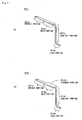
FIGS. 6A and 6B show arrangement of contacts of the electric connector, whereFIG. 6A is a schematic plan view andFIG. 6B is a schematic bottom view; and -
FIG. 7A is a schematic perspective view of a first or a second contact of the electric connector, andFIG. 7B is a schematic perspective view of a second contact at an outermost end of the electric connector. - In the description which follows, relative spatial terms such as "upper", "lower", "downward", "under", "bottom", etc., are used for the convenience of the skilled reader and refer to the orientation of the connector or contacts and their constituent parts as depicted in the drawings. No limitation is intended by use of these terms, either in use of the invention, during its manufacture, shipment, custody, or sale, or during assembly of its constituent parts or when incorporated into or combined with other apparatus.
- The electric connector shown in
FIGS. 1 to 3 is a receptacle adapted to be mounted to a circuit board, capable of high-speed differential signaling. The electric connector includes aninsulative body 100, upper and lower groups ofcontacts 200a and 200b, and ashield cover 300 covering the outer periphery of thebody 100. The upper and lower groups ofcontacts 200a and 200b are disposed in spaced relationship inside the body and arranged in two rows in a lateral direction of thebody 100 in a staggered or zigzag manner. Each of the components of the electric connector is detailed in the following description. - In the drawings and in the following paragraphs, first or upper contacts and their features have an "a" suffix, and second or lower contacts and their features have a "b" suffix. Similarly, sets of first (upper) and second (lower) terminal insertion holes provided in the electrical connector are denoted by 111a and 111b, respectively.
- As shown in
FIGS. 1 ,3A ,3B ,4 and5 , thebody 100 is formed from a synthetic resin for general use such as PBT (polybutylene terephthalate) or PPS (polyphenylene sulfide) by injection molding. Thebody 100 can be mated with a plug A, shown in dotted outine inFIG. 5 . - The
body 100 includes a connectormain portion 110 having a substantially rectangular solid shape, a projectingportion 120 having a substantially inverted-U shape as viewed from the front, abase 130 having a substantially plate-like shape, and acylindrical boss 140. The projectingportion 120 is provided at the front side of the connectormain portion 110 and adapted to enter into a recess provided at a tip end of the plug A. Thebase 130 is provided under the connectormain portion 110 and extended forward. Theboss 140 is formed downward on a bottom surface of thebase 130 and fits into a hole (not shown) in the circuit board. - In a central portion of the connector
main portion 110 of thebody 100,terminal insertion holes FIG. 1 , the widthwise ends of the firstterminal insertion holes 111a are located in such plan positions as to overlap the widthwise ends of the secondterminal insertion holes 111b. - The
terminal insertion holes main portions contacts 200a and 200b. Of the twenty terminal insertion holes, all holes other than aterminal insertion hole 111b' at the rightmost end in the lower row inFIG. 1 are identical to one another. Theterminal insertion hole 111b' at the rightmost end is a through hole of a horizontally elongated rectangular shape, is wider than the otherterminal insertion holes main portion 2012b in the lower group ofcontacts 200b. Regarding theterminal insertion hole 111b' at the rightmost end, an apostrophe is added to the reference numeral as above for distinction from the otherterminal insertion holes 111b. - As shown in
FIGS. 3B and5 , acutout 112 is provided in the rear surface of the connectormain portion 110. In the inner back surface of thecutout 112, there are linearterminal insertion grooves 113 extending downward under the respectiveterminal insertion holes terminal insertion grooves 113 are long grooves arranged in the lateral direction of the body. Theterminal insertion grooves 113 correspond in lateral width to lead-outportions contacts 200a and 200b. - As shown in
FIG. 1 , in an upper surface of the projectingportion 120 of thebody 100, there are providedterminal guide grooves 121a communicating with theterminal insertion holes 111a in the connectormain portion 110 and extending in straight lines in a longitudinal direction of thebody 100. In the lower surface of the projectingportion 120, there are providedterminal guide grooves 121b communicating with the terminal insertion holes 111b in themain portion 110 and extending in straight lines in a longitudinal direction of thebody 100. Theterminal guide grooves portions contacts 200a and 200b. Theterminal guide grooves terminal insertion holes - The
shield cover 300, as shown inFIGS. 1 to 3B , is a metal shell which can be brought into contact with an outer peripheral shield (not shown) of the plug A as mated with thebody 100. Theshield cover 300 includes a covermain body 310, a pair oflegs 320 extending downward from opposite widthwise ends of thecover body 310, and aback cover 330 for openably covering an opening on the back side of thecover body 310. - The
cover body 310, shaped as a substantially square cylinder, fits about the connectormain portion 110 of thebody 100 so as to cover four sides - upper, lower, right and left sides - of the connectormain portion 110 and the projecting portion 120 (i.e., the outer peripheries of the connectormain portion 110 and the projecting portion 120). - The
legs 320 are adapted to be inserted into attachment holes (not shown) in the circuit board and connected to a ground pattern on the circuit board. - The
back cover 330 is a plate-like member that has its upper end pivotably attached to an upper edge of the opening on the rear side of the covermain body 310. Theback cover 330 closes the opening on the rear side of the covermain body 310 so as to cover the rear side of the connectormain portion 110 of thebody 100. - As shown in
FIGS. 6A and 6B , the upper contact group 200a consists ofcontacts 201a-210a. Thelower contact group 200b consists ofcontacts 201b-210b. - As shown in
FIGS. 6A to 7B , thecontact 201a is representative of the contacts in the upper contact group 200a and includes acontact portion 2011a, a contactmain portion 2012a, a lead-outportion 2013a, and alead portion 2014a. Thecontact portion 2011a is a plate-like portion that can be brought into contact with a contact (not shown) of the plug A as engaged with the projectingportion 120 of thebody 100. The contactmain portion 2012a, a plate-like portion with a larger width than that of thecontact portion 2011a, is provided continuously from or integral with the rear end of thecontact portion 2011a and is adapted to be press fitted into the associatedterminal insertion hole 111a in thebody 100. The lead-outportion 2013a, a rod-like portion provided continuously from or integral with the rear end of the contactmain portion 2012a, is bent substantially at a right angle so as to extend along the rear surface of thebody 100. Thelead portion 2014a, a rod-like portion provided continuously from or integral with the rear end of the lead-outportion 2013a, is bent substantially at a right angle so as to be connected to a pattern on the circuit board. - The
contact 202b is one of the contacts in thelower contact group 200b and includes acontact portion 2021b, a contactmain portion 2022b, a lead-outportion 2023b, and alead portion 2024b. Thecontact portion 2021b is a plate-like portion which can be brought into contact with a contact (not shown) of the plug A as engaged with the projectingportion 120 of thebody 100. The contactmain portion 2022b, a plate-like portion with a larger width than that of thecontact portion 2021b, is provided continuously from or integral with the rear end of thecontact portion 2021b and is adapted to be press fitted into the associatedterminal insertion hole 111b in thebody 100. The lead-outportion 2023b, a rod-like portion provided continuously from or integral with the rear end of the contactmain portion 2022b, is bent substantially at a right angle so as to extend along the rear surface of thebody 100. Thelead portion 2024b, a rod-like portion provided continuously from or integral with the rear end of the lead-outportion 2023b, is bent substantially at a right angle so as to be connected to the pattern on the circuit board. - As shown in
FIG. 3B , the contacts of the upper group 200a such ascontact 201a and the contacts of thelower group 200b such ascontact 202b are different from each other in that the lead-outportion 2013a is longer than the respective lead-outportion 2023b by the length of distance between the upper row and the lower row.Contacts contact 201a. - As shown in
FIG. 6A ,contacts contact 201a except that theircontact portions contact portion 2011a of thecontact 201a. -
Contacts contact 202b.Contacts contact 202b except that theircontact portions contact portion 2021b of thecontact 202b. - As shown in
FIG. 6B , acontact 201b is the same as thecontact 202b, except that itscontact portion 2011b is longer than thecontact portion 2021b of thecontact 202b and that it has a plate-like extended portion 2012b1 along a widthwise end of themain portion 2012b. - The electric connector according to the present embodiment is used as a power source line and also used for transmission of single end signals and first to fifth differential signals. The
contacts contacts contacts contacts - Among the upper and lower groups of
contacts 200a and 200b, of special note are thecontacts 201a-206a, 208a, 209a, 201b-206b and 208b for transmission of the first to fifth differential signals. As shown inFIG. 1 , these contacts are disposed in five sets of triangular arrangements on a cross sectional plain of the body 100: each triangular set or group of three contacts is formed by one positive signal contact and one negative signal contact disposed at one side of the triangular arrangement and one common ground contact disposed at the opposite apex. These five sets are sequentially arranged in the lateral direction of thebody 100 with their vertical orientations alternately inverted. - In the electric connector in the present embodiment, the contacts for signal transmission and other use are arranged in the above-described relationship. Therefore, for the purpose of reducing a skew, etc. between adjacent contacts of each differential pair and between the differential pairs, the longitudinal relationship among the
contact portions 2011a-2111a of thecontacts 201a-210a and thecontact portions 2011b-2111b of thecontacts 201b-210b is established as shown inFIGS. 6A and 6B . - The
contacts 201a-210a are positioned and inserted into ten associatedterminal insertion holes 111a in thebody 100 from the rear side of thebody 100. Then, thecontact portions 2011a-2101a of thecontacts 201a-210a are received in the respective tenterminal guide grooves 121a in thebody 100. Simultaneously therewith, the contactmain portions 2012a-2102a of thecontacts 201a-210a are press fitted within the respective tenterminal insertion holes 111a, and the lead-outportions 2013a-2103a are received in the respective tenterminal insertion grooves 113. - Meanwhile, the
contacts 201b-210b are positioned and inserted into theterminal insertion hole 111b' and the nine terminal insertion holes 111b in thebody 100, respectively, from the rear side of thebody 100. Then, thecontact portions 2011b-2101b of thecontacts 201b-210b are received in the respective tenterminal guide grooves 121b in thebody 100. Simultaneously therewith, the contactmain portions 2012b-2102b of thecontacts 201b-210b are press fitted within theterminal insertion hole 111b' and the nineterminal insertion holes 111b, respectively, and the lead-outportions 2013b to 2103b are received in the remaining tenterminal insertion grooves 113. - As shown in
FIGS. 6A and 6B , in the upper contact group 200a and thelower contact group 200b as fixed to thebody 100 in the above-described manner, the widthwise ends of the contactmain portions 2012a-2102a of thecontacts 201a-210a are located in such plain positions as to overlap the widthwise ends of the contactmain portions 2012b-2102b of thecontacts 201b-210b. - As a consequence, in any one of the common ground contacts, opposite widthwise ends of the contact main portion are located in such plain positions as to overlap an inner widthwise end of the contact main portion of the adjacent plus signal contact and an inner widthwise end of the contact main portion of the minus signal contact. In addition, adjacent to these plus signal contacts and minus signal contacts, the common ground contacts in other sets are arranged. This arrangement of the contacts achieves excellently matched impedances in the respective differential pairs of contacts.
- The overlapping width and area (N1) of the extended portion 2012b1 of the contact
main portion 2012b of thecontact 201b overlapping the contactmain portion 2012a of thecontact 201a is approximately twice as large as each overlapping width and area (N2) of the ends of contact main portions of any other two contacts for differential signaling (i.e., the outer end and the inner end in each triangular set-for example, an end of the contactmain portion 2032a of thecontact 203a and an end of the contactmain portion 2022b of thecontact 202b that are next to each other). In this manner, adjustment is made to the width and area of the contactmain portion 2012b of thecontact 201b, in accordance with the difference in impedance from other signal contacts with respect to common ground contacts. This structure prevents reduction in capacitance between thecontact 201a and thecontact 201b that should have been created due to the location of thecontact 201a at the outmost end of the upper group of contacts 200a and absence of a neighboring common ground contact. Consequently, it becomes possible to suppress variation in impedance within the differential pair located at the outmost end of the groups of contacts, providing matched impedances. - With the electric connector as described above, impedance can be matched within the differential pair at an outmost end of the groups of contacts without adding a dummy ground contact or changing the shape of the
shield cover 300 as has been previously described. Matched impedances within each pair should result in matched impedances among the differential pairs. Accordingly, the transmission characteristics of the electric connector can be improved without increase in costs. - It should be noted that any change in design can be made to the above-described electric connector as long as it includes an insulative body and groups of contacts disposed in spaced relationship inside the body, the contacts being arranged in at least two rows in a lateral direction of the body, as long as the groups of contacts include a plurality of first contacts; and a plurality of second contacts located in a different row from a row where their associated first contacts exist, the second contacts being arranged next to the first contacts, and as long as, out of one of the first contacts and one of the second contacts subject to impedance tuning, one of these two contacts has a width and an area thereof adjusted in accordance with a difference in impedance from impedances between other first and second contacts.
- Although it is described in the above-described embodiment that adjustment is made to the width and area of the common ground contact located at an outermost end in the groups of contacts, the present invention is not limited thereto. For instance, the width and area of the
main portion 2012a of thecontact 201a, which is a signal contact, may be reduced as compared with other signal contacts, thereby preventing reduction in capacitance between thecontacts - Further, although it is described in the above-described embodiment that the contacts subject to impedance tuning are the
contacts - The present electric connector can be applied to an electric connector for unbalanced (single-ended) signaling. More particularly, adjustment may be made to a single-ended signal contact and a ground contact thereof subject to impedance tuning, by adjusting a width and area of one of these two contacts in accordance with the difference in impedance from another set of a single-ended signal contact and a ground contact.
- The geometry of the contacts is not limited to one described in the above-described embodiment, and any change in design can be made.
- The arrangement design of the contacts can be changed as appropriate, so long as the contacts are arranged with spacing in at least two rows in the lateral direction inside the body. In the case where the present electric connector is an electric connector for differential signaling, it is preferable that, with a positive signal contact, a negative signal contact, and a common ground contact constituting a set in a triangular arrangement as described above, a plurality of such sets is arranged one set after another in the lateral direction; however, the present invention is not limited thereto. The contact arrangement may be modified such that, for example, a plurality of positive and negative signal contacts is arranged in a first row, and a plurality of common ground contacts is arranged in a second row. The contacts can also be arranged such that their widthwise ends do not overlap one another in their plain positions.
- In addition, although the above electric connector is described as a receptacle, it may alternatively be a plug having contacts connected to a cable.
-
- 100
- BODY
- 200a
- UPPER GROUP OF CONTACTS
- 201a
- CONTACT (ONE OF FIRST CONTACTS)
2011a CONTACT PORTION
2012a MAIN PORTION
2013a LEAD-OUT PORTION
2014a LEAD PORTION - 202a
- CONTACT (THE OTHER OF FIRST CONTACTS)
2021a CONTACT PORTION
2022a MAIN PORTION
2023a LEAD-OUT PORTION
2024a LEAD PORTION - 200b
- LOWER GROUP OF CONTACTS
- 202b
- CONTACT (SECOND)
- 2011b
- CONTACT PORTION
- 2012b
- MAIN PORTION
2012b1 EXTENDED PORTION - 2013b
- LEAD-OUT PORTION
- 2014b
- LEAD PORTION
Claims (4)
- An electric connector comprising:an insulative body (100); andgroups of contacts (200a,200b) disposed in spaced relationship inside the body, the contacts being arranged in at least two rows in a lateral direction of the body, whereinthe groups of contacts include:a plurality of first contacts (201a, 202a, 204a, 205a, 208a, 209a, 202b, 203b, 205b, 206b); anda plurality of second contacts (203a, 206a, 201b, 204b, 208b) located in a different row from a row having associated first contacts, the second contacts being arranged next to the first contacts,the first contacts each include:a first contact main portion (2012a, 2022a, 2042a, 2052a, 2082a, 2092a, 2022b, 2032b, 2052b, 2062b) adapted to be held in the body (100);a first contact portion (2011a, 2021a, 2041a, 2051a, 2081a, 2091a, 2021b, 2031b, 2051b, 2061b) continuous from a distal end of the first contact main portion and exposed from a first end in a longitudinal direction of the body;a first lead-out portion (2013a, 2023a, 2043a, 2053a, 2083a, 2093a, 2023b, 2033b, 2053b, 2063b) continuous from a rear end of the first contact main portion and exposed from a second end in the longitudinal direction of the body; anda first lead portion (2014a, 2024a, 2044a, 2054a, 2084a, 2094a, 2024b, 2034b, 2054b, 2064b) continuous from a rear end of the first lead-out portion,the second contacts (203a, 206a, 201b, 204b, 208b) each include:a second contact main portion (2032a, 2062a, 2012b, 2042b, 2082b) adapted to be held in the body, a widthwise end of the second contact main portion being located in such a plain position as to overlap a widthwise end of the first contact main portion of the nearest first contact;a second contact portion (2031a, 2061a, 2011b, 2041b, 2081b) continuous from a distal end of the second contact main portion and exposed from the first end in a longitudinal direction of the body;a second lead-out portion (2033a, 2063a, 2013b, 2043b, 2083b) continuous from a rear end of the second contact main portion and exposed from the second end in the longitudinal direction of the body; anda second lead portion (2034a, 2064a, 2014b, 2044b, 2084b) continuous from a rear end of the second lead-out portion; andone (201a) of the first contacts and one (201b) of the second contacts at an outermost end in said groups of contacts arranged in the lateral direction of the body (100) are subject to impedance tuning;characterised in that:an overlapping width and area N1 is larger than an overlapping width and area N2, wherein N1 is an overlapping width and area where an outer end (2012b1) of a second contact main portion (2012b) of a second contact (201b) at an outermost end of the groups of contacts overlaps, in plain position, the first contact main portion (2012a) of the first contact (201a) at the outermost end, and N2 is an overlapping width and area where an outer end of a second contact main portion (2032a, 2062a, 2042b, 2082b) of another second contact overlaps, in plain position, an inner end of a first contact main portion (2022a, 2042a, 2052a, 2082a, 2092a, 2022b, 2032b, 2052b, 2062b) of another first contact (202a-210a).
- The electric connector according to claim 1, wherein
the groups of contacts are arranged such that a plurality of sets (201a,201b,202a; 202b,203a,203b; 204a,204b,205a; 205b,206a,206b; 208a,208b,209a) is disposed in the lateral direction of the body (100) with respective vertical positional relationships of the sets turned upside down alternately, each of the sets being made up by a pair of signal contacts (201a,202a; 202b,203b; 204a,205a; 205b,206b; 208a,209a) from one row and a ground contact (201b; 203a; 209b; 206a; 208b) from a different row. - The electric connector according to claim 2, wherein
in each of the sets, widthwise ends of the ground contact are so positioned as to overlap widthwise inner ends of the pair of signal contacts in plain position. - The electric connector according to any one of the preceding claims, wherein
the first contacts (201a, 202a, 204a, 205a, 208a, 209a, 202b, 203b, 205b, 206b) are signal contacts, and
the second contacts (203a, 206a, 201b, 204b, 208b) are ground contacts.
Applications Claiming Priority (1)
| Application Number | Priority Date | Filing Date | Title |
|---|---|---|---|
| JP2007184049A JP4932626B2 (en) | 2007-07-13 | 2007-07-13 | Electrical connector |
Publications (3)
| Publication Number | Publication Date |
|---|---|
| EP2015402A2 EP2015402A2 (en) | 2009-01-14 |
| EP2015402A3 EP2015402A3 (en) | 2013-02-13 |
| EP2015402B1 true EP2015402B1 (en) | 2014-03-19 |
Family
ID=39863086
Family Applications (1)
| Application Number | Title | Priority Date | Filing Date |
|---|---|---|---|
| EP08252372.1A Active EP2015402B1 (en) | 2007-07-13 | 2008-07-11 | Electric connector |
Country Status (6)
| Country | Link |
|---|---|
| US (1) | US7670199B2 (en) |
| EP (1) | EP2015402B1 (en) |
| JP (1) | JP4932626B2 (en) |
| KR (1) | KR101383140B1 (en) |
| CN (1) | CN101345374B (en) |
| TW (1) | TWI433396B (en) |
Families Citing this family (29)
| Publication number | Priority date | Publication date | Assignee | Title |
|---|---|---|---|---|
| CN201117870Y (en) * | 2007-11-12 | 2008-09-17 | 富士康(昆山)电脑接插件有限公司 | Electric Connector |
| JP4647675B2 (en) * | 2008-07-22 | 2011-03-09 | ホシデン株式会社 | connector |
| TWM357080U (en) * | 2008-12-24 | 2009-05-11 | Advanced Connectek Inc | Socket connector |
| JP4795444B2 (en) | 2009-02-09 | 2011-10-19 | ホシデン株式会社 | connector |
| JP2010244901A (en) * | 2009-04-07 | 2010-10-28 | Japan Aviation Electronics Industry Ltd | Connector |
| JP5342943B2 (en) | 2009-06-29 | 2013-11-13 | ホシデン株式会社 | Multi-pole connector |
| JP5351751B2 (en) * | 2009-12-25 | 2013-11-27 | ホシデン株式会社 | connector |
| CN102195173B (en) | 2010-02-15 | 2015-06-10 | 莫列斯公司 | Differentially coupled connector |
| JP5634095B2 (en) * | 2010-03-31 | 2014-12-03 | ホシデン株式会社 | Connector and printed circuit board foot pattern for connector |
| JP5554619B2 (en) * | 2010-04-13 | 2014-07-23 | 富士通コンポーネント株式会社 | connector |
| JP5502233B2 (en) * | 2010-04-14 | 2014-05-28 | モレックス インコーポレイテド | Multilayer connector |
| JP5629495B2 (en) | 2010-06-01 | 2014-11-19 | ホシデン株式会社 | connector |
| JP2012054215A (en) | 2010-09-03 | 2012-03-15 | Yazaki Corp | Connector |
| JP5727902B2 (en) * | 2011-09-13 | 2015-06-03 | ホシデン株式会社 | connector |
| US11165208B2 (en) | 2011-09-28 | 2021-11-02 | 3M Innovative Properties Company | Electrical contact and connector |
| JP5605378B2 (en) * | 2012-01-18 | 2014-10-15 | Smk株式会社 | Electrical connector |
| JP5830394B2 (en) * | 2012-01-26 | 2015-12-09 | ホシデン株式会社 | Contact impedance adjustment method, contact and connector equipped with the same |
| JP5699110B2 (en) * | 2012-05-28 | 2015-04-08 | 京セラコネクタプロダクツ株式会社 | connector |
| WO2014113563A1 (en) * | 2013-01-16 | 2014-07-24 | Molex Incorporated | Low profile connector system |
| JP6133107B2 (en) * | 2013-04-08 | 2017-05-24 | 日本航空電子工業株式会社 | Plug connector |
| EP2821988A1 (en) * | 2013-07-02 | 2015-01-07 | Samsung Electronics Co., Ltd | Connector for reducing near-end crosstalk |
| JP6206713B2 (en) | 2013-10-01 | 2017-10-04 | パナソニックIpマネジメント株式会社 | connector |
| CN104158025A (en) * | 2014-08-26 | 2014-11-19 | 苏州祥龙嘉业电子科技有限公司 | Connector socket used for transmitting high-definition digital signals |
| KR102096440B1 (en) * | 2014-09-25 | 2020-04-02 | 엘에스엠트론 주식회사 | Receptacle connector inculuding the improved contact array structure |
| CN104518321B (en) * | 2014-11-27 | 2023-05-05 | 连展科技电子(昆山)有限公司 | Plug electric connector |
| CN107206896B (en) * | 2014-12-22 | 2021-03-05 | 大众汽车有限公司 | Finger strip and use of a finger strip |
| CN104538797B (en) * | 2014-12-23 | 2023-11-17 | 连展科技电子(昆山)有限公司 | Anti-interference plug electric connector |
| CN205882228U (en) * | 2016-07-27 | 2017-01-11 | 广东欧珀移动通信有限公司 | Power source , mobile terminal and power adapter |
| CN111224269B (en) * | 2020-01-13 | 2021-05-25 | 番禺得意精密电子工业有限公司 | Electrical connector |
Family Cites Families (10)
| Publication number | Priority date | Publication date | Assignee | Title |
|---|---|---|---|---|
| US6439931B1 (en) * | 1998-05-13 | 2002-08-27 | Molex Incorporated | Method and structure for tuning the impedance of electrical terminals |
| US6368155B1 (en) * | 1999-07-16 | 2002-04-09 | Molex Incorporated | Intelligent sensing connectors |
| US6454605B1 (en) * | 1999-07-16 | 2002-09-24 | Molex Incorporated | Impedance-tuned termination assembly and connectors incorporating same |
| TW456619U (en) * | 1999-07-16 | 2001-09-21 | Molex Inc | Impedance-tuned termination assembly and connectors incorporating same |
| EP1196967B1 (en) * | 1999-07-16 | 2004-09-29 | Molex Incorporated | Impedance-tuned connector |
| JP3495007B2 (en) * | 2001-03-14 | 2004-02-09 | 日本航空電子工業株式会社 | High-speed transmission connector |
| JP3987493B2 (en) * | 2001-08-01 | 2007-10-10 | モレックス インコーポレーテッド | Impedance adjusted connector |
| JP4091603B2 (en) * | 2002-06-21 | 2008-05-28 | モレックス インコーポレーテッド | Impedance tuned high density connector with modular structure |
| JP2007080782A (en) * | 2005-09-16 | 2007-03-29 | Japan Aviation Electronics Industry Ltd | Electric connector |
| CN101162806B (en) * | 2006-10-12 | 2011-01-12 | 富士康(昆山)电脑接插件有限公司 | Electrical connector |
-
2007
- 2007-07-13 JP JP2007184049A patent/JP4932626B2/en active Active
-
2008
- 2008-05-19 TW TW097118382A patent/TWI433396B/en active
- 2008-06-24 US US12/144,965 patent/US7670199B2/en active Active
- 2008-06-27 KR KR1020080061824A patent/KR101383140B1/en active IP Right Grant
- 2008-07-11 CN CN2008101303326A patent/CN101345374B/en active Active
- 2008-07-11 EP EP08252372.1A patent/EP2015402B1/en active Active
Also Published As
| Publication number | Publication date |
|---|---|
| TWI433396B (en) | 2014-04-01 |
| JP4932626B2 (en) | 2012-05-16 |
| US20090017646A1 (en) | 2009-01-15 |
| KR101383140B1 (en) | 2014-04-09 |
| CN101345374A (en) | 2009-01-14 |
| EP2015402A2 (en) | 2009-01-14 |
| KR20090007213A (en) | 2009-01-16 |
| CN101345374B (en) | 2012-10-10 |
| JP2009021152A (en) | 2009-01-29 |
| TW200908453A (en) | 2009-02-16 |
| US7670199B2 (en) | 2010-03-02 |
| EP2015402A3 (en) | 2013-02-13 |
Similar Documents
| Publication | Publication Date | Title |
|---|---|---|
| EP2015402B1 (en) | Electric connector | |
| EP2015401B1 (en) | Electric connector | |
| EP1897178B1 (en) | Electrical connector | |
| US6379188B1 (en) | Differential signal electrical connectors | |
| KR100930846B1 (en) | Electrical components with contact terminals arranged in a general trapezoidal shape | |
| US6572410B1 (en) | Connection header and shield | |
| EP0446980B2 (en) | Connector assembly for printed circuit boards | |
| EP0994535B1 (en) | Modular connector with reduced crosstalk | |
| AU2009248414A1 (en) | Circuit board for electrical connector and electrical connector | |
| KR20020020783A (en) | Impedance-tuned connector | |
| US10418753B2 (en) | Connector assembly with low pair cross talk | |
| CN101351932B (en) | Differential transmission connector and differential transmission connector for fixing substrate fitted to it | |
| CN105207012A (en) | Electrical connector having common ground shield | |
| US11411356B2 (en) | Electrical cable connector assembly with a grounding layer clamped to a circuit board | |
| CN110021832A (en) | Stacked twin connectors system | |
| EP2015400B1 (en) | Contact, and electric connector using the same | |
| US7798854B2 (en) | Connector | |
| US20120329322A1 (en) | Connector and signal line structure | |
| US20130196541A1 (en) | Contact impedance adjusting method, contact, and connector having the same | |
| JPH0524137Y2 (en) | ||
| AU732218B3 (en) | Multi-contact electrical connector |
Legal Events
| Date | Code | Title | Description |
|---|---|---|---|
| PUAI | Public reference made under article 153(3) epc to a published international application that has entered the european phase |
Free format text: ORIGINAL CODE: 0009012 |
|
| AK | Designated contracting states |
Kind code of ref document: A2 Designated state(s): AT BE BG CH CY CZ DE DK EE ES FI FR GB GR HR HU IE IS IT LI LT LU LV MC MT NL NO PL PT RO SE SI SK TR |
|
| AX | Request for extension of the european patent |
Extension state: AL BA MK RS |
|
| PUAL | Search report despatched |
Free format text: ORIGINAL CODE: 0009013 |
|
| AK | Designated contracting states |
Kind code of ref document: A3 Designated state(s): AT BE BG CH CY CZ DE DK EE ES FI FR GB GR HR HU IE IS IT LI LT LU LV MC MT NL NO PL PT RO SE SI SK TR |
|
| AX | Request for extension of the european patent |
Extension state: AL BA MK RS |
|
| 17P | Request for examination filed |
Effective date: 20130726 |
|
| RBV | Designated contracting states (corrected) |
Designated state(s): AT BE BG CH CY CZ DE DK EE ES FI FR GB GR HR HU IE IS IT LI LT LU LV MC MT NL NO PL PT RO SE SI SK TR |
|
| AKX | Designation fees paid |
Designated state(s): DE FR GB |
|
| REG | Reference to a national code |
Ref country code: DE Ref legal event code: R079 Ref document number: 602008030945 Country of ref document: DE Free format text: PREVIOUS MAIN CLASS: H01R0012200000 Ipc: H01R0013647400 |
|
| GRAP | Despatch of communication of intention to grant a patent |
Free format text: ORIGINAL CODE: EPIDOSNIGR1 |
|
| RIC1 | Information provided on ipc code assigned before grant |
Ipc: H01R 13/6474 20110101AFI20131021BHEP |
|
| INTG | Intention to grant announced |
Effective date: 20131111 |
|
| GRAS | Grant fee paid |
Free format text: ORIGINAL CODE: EPIDOSNIGR3 |
|
| GRAA | (expected) grant |
Free format text: ORIGINAL CODE: 0009210 |
|
| AK | Designated contracting states |
Kind code of ref document: B1 Designated state(s): DE FR GB |
|
| REG | Reference to a national code |
Ref country code: GB Ref legal event code: FG4D |
|
| REG | Reference to a national code |
Ref country code: DE Ref legal event code: R096 Ref document number: 602008030945 Country of ref document: DE Effective date: 20140430 |
|
| REG | Reference to a national code |
Ref country code: DE Ref legal event code: R097 Ref document number: 602008030945 Country of ref document: DE |
|
| PLBE | No opposition filed within time limit |
Free format text: ORIGINAL CODE: 0009261 |
|
| STAA | Information on the status of an ep patent application or granted ep patent |
Free format text: STATUS: NO OPPOSITION FILED WITHIN TIME LIMIT |
|
| 26N | No opposition filed |
Effective date: 20141222 |
|
| REG | Reference to a national code |
Ref country code: DE Ref legal event code: R097 Ref document number: 602008030945 Country of ref document: DE Effective date: 20141222 |
|
| REG | Reference to a national code |
Ref country code: FR Ref legal event code: PLFP Year of fee payment: 9 |
|
| REG | Reference to a national code |
Ref country code: FR Ref legal event code: PLFP Year of fee payment: 10 |
|
| REG | Reference to a national code |
Ref country code: FR Ref legal event code: PLFP Year of fee payment: 11 |
|
| REG | Reference to a national code |
Ref country code: DE Ref legal event code: R082 Ref document number: 602008030945 Country of ref document: DE Representative=s name: ETL IP PATENTANWALTSGESELLSCHAFT MBH, DE Ref country code: DE Ref legal event code: R082 Ref document number: 602008030945 Country of ref document: DE Representative=s name: ETL IP PATENT- UND RECHTSANWALTSGESELLSCHAFT M, DE Ref country code: DE Ref legal event code: R082 Ref document number: 602008030945 Country of ref document: DE Representative=s name: ETL WABLAT & KOLLEGEN PATENT- UND RECHTSANWALT, DE |
|
| REG | Reference to a national code |
Ref country code: DE Ref legal event code: R082 Ref document number: 602008030945 Country of ref document: DE Representative=s name: ETL IP PATENTANWALTSGESELLSCHAFT MBH, DE Ref country code: DE Ref legal event code: R082 Ref document number: 602008030945 Country of ref document: DE Representative=s name: ETL IP PATENT- UND RECHTSANWALTSGESELLSCHAFT M, DE |
|
| PGFP | Annual fee paid to national office [announced via postgrant information from national office to epo] |
Ref country code: GB Payment date: 20220606 Year of fee payment: 15 |
|
| PGFP | Annual fee paid to national office [announced via postgrant information from national office to epo] |
Ref country code: FR Payment date: 20220609 Year of fee payment: 15 |
|
| PGFP | Annual fee paid to national office [announced via postgrant information from national office to epo] |
Ref country code: DE Payment date: 20220531 Year of fee payment: 15 |
|
| REG | Reference to a national code |
Ref country code: DE Ref legal event code: R119 Ref document number: 602008030945 Country of ref document: DE |
|
| GBPC | Gb: european patent ceased through non-payment of renewal fee |
Effective date: 20230711 |
|
| PG25 | Lapsed in a contracting state [announced via postgrant information from national office to epo] |
Ref country code: DE Free format text: LAPSE BECAUSE OF NON-PAYMENT OF DUE FEES Effective date: 20240201 Ref country code: GB Free format text: LAPSE BECAUSE OF NON-PAYMENT OF DUE FEES Effective date: 20230711 |