EP2015362A1 - Semiconductor array and manufacturing method thereof - Google Patents
Semiconductor array and manufacturing method thereof Download PDFInfo
- Publication number
- EP2015362A1 EP2015362A1 EP07301083A EP07301083A EP2015362A1 EP 2015362 A1 EP2015362 A1 EP 2015362A1 EP 07301083 A EP07301083 A EP 07301083A EP 07301083 A EP07301083 A EP 07301083A EP 2015362 A1 EP2015362 A1 EP 2015362A1
- Authority
- EP
- European Patent Office
- Prior art keywords
- cells
- cell
- rows
- lines
- coupled
- Prior art date
- Legal status (The legal status is an assumption and is not a legal conclusion. Google has not performed a legal analysis and makes no representation as to the accuracy of the status listed.)
- Withdrawn
Links
- 239000004065 semiconductor Substances 0.000 title claims abstract description 23
- 238000004519 manufacturing process Methods 0.000 title claims description 3
- 239000011159 matrix material Substances 0.000 claims abstract description 20
- 238000005516 engineering process Methods 0.000 claims description 10
- 238000000034 method Methods 0.000 claims description 4
- 238000003491 array Methods 0.000 description 5
- XUIMIQQOPSSXEZ-UHFFFAOYSA-N Silicon Chemical compound [Si] XUIMIQQOPSSXEZ-UHFFFAOYSA-N 0.000 description 3
- 238000009413 insulation Methods 0.000 description 3
- 229910052710 silicon Inorganic materials 0.000 description 3
- 239000010703 silicon Substances 0.000 description 3
- 239000003990 capacitor Substances 0.000 description 2
- 230000000295 complement effect Effects 0.000 description 1
- 239000012212 insulator Substances 0.000 description 1
- 238000002955 isolation Methods 0.000 description 1
- 239000000463 material Substances 0.000 description 1
- 238000012986 modification Methods 0.000 description 1
- 230000004048 modification Effects 0.000 description 1
- 229920000747 poly(lactic acid) Polymers 0.000 description 1
Images


Classifications
-
- H—ELECTRICITY
- H01—ELECTRIC ELEMENTS
- H01L—SEMICONDUCTOR DEVICES NOT COVERED BY CLASS H10
- H01L27/00—Devices consisting of a plurality of semiconductor or other solid-state components formed in or on a common substrate
- H01L27/02—Devices consisting of a plurality of semiconductor or other solid-state components formed in or on a common substrate including semiconductor components specially adapted for rectifying, oscillating, amplifying or switching and having at least one potential-jump barrier or surface barrier; including integrated passive circuit elements with at least one potential-jump barrier or surface barrier
- H01L27/04—Devices consisting of a plurality of semiconductor or other solid-state components formed in or on a common substrate including semiconductor components specially adapted for rectifying, oscillating, amplifying or switching and having at least one potential-jump barrier or surface barrier; including integrated passive circuit elements with at least one potential-jump barrier or surface barrier the substrate being a semiconductor body
- H01L27/10—Devices consisting of a plurality of semiconductor or other solid-state components formed in or on a common substrate including semiconductor components specially adapted for rectifying, oscillating, amplifying or switching and having at least one potential-jump barrier or surface barrier; including integrated passive circuit elements with at least one potential-jump barrier or surface barrier the substrate being a semiconductor body including a plurality of individual components in a repetitive configuration
- H01L27/105—Devices consisting of a plurality of semiconductor or other solid-state components formed in or on a common substrate including semiconductor components specially adapted for rectifying, oscillating, amplifying or switching and having at least one potential-jump barrier or surface barrier; including integrated passive circuit elements with at least one potential-jump barrier or surface barrier the substrate being a semiconductor body including a plurality of individual components in a repetitive configuration including field-effect components
-
- G—PHYSICS
- G11—INFORMATION STORAGE
- G11C—STATIC STORES
- G11C11/00—Digital stores characterised by the use of particular electric or magnetic storage elements; Storage elements therefor
- G11C11/21—Digital stores characterised by the use of particular electric or magnetic storage elements; Storage elements therefor using electric elements
- G11C11/34—Digital stores characterised by the use of particular electric or magnetic storage elements; Storage elements therefor using electric elements using semiconductor devices
- G11C11/40—Digital stores characterised by the use of particular electric or magnetic storage elements; Storage elements therefor using electric elements using semiconductor devices using transistors
- G11C11/401—Digital stores characterised by the use of particular electric or magnetic storage elements; Storage elements therefor using electric elements using semiconductor devices using transistors forming cells needing refreshing or charge regeneration, i.e. dynamic cells
- G11C11/402—Digital stores characterised by the use of particular electric or magnetic storage elements; Storage elements therefor using electric elements using semiconductor devices using transistors forming cells needing refreshing or charge regeneration, i.e. dynamic cells with charge regeneration individual to each memory cell, i.e. internal refresh
- G11C11/4023—Digital stores characterised by the use of particular electric or magnetic storage elements; Storage elements therefor using electric elements using semiconductor devices using transistors forming cells needing refreshing or charge regeneration, i.e. dynamic cells with charge regeneration individual to each memory cell, i.e. internal refresh using field effect transistors
-
- G—PHYSICS
- G11—INFORMATION STORAGE
- G11C—STATIC STORES
- G11C11/00—Digital stores characterised by the use of particular electric or magnetic storage elements; Storage elements therefor
- G11C11/21—Digital stores characterised by the use of particular electric or magnetic storage elements; Storage elements therefor using electric elements
- G11C11/34—Digital stores characterised by the use of particular electric or magnetic storage elements; Storage elements therefor using electric elements using semiconductor devices
- G11C11/40—Digital stores characterised by the use of particular electric or magnetic storage elements; Storage elements therefor using electric elements using semiconductor devices using transistors
- G11C11/401—Digital stores characterised by the use of particular electric or magnetic storage elements; Storage elements therefor using electric elements using semiconductor devices using transistors forming cells needing refreshing or charge regeneration, i.e. dynamic cells
- G11C11/402—Digital stores characterised by the use of particular electric or magnetic storage elements; Storage elements therefor using electric elements using semiconductor devices using transistors forming cells needing refreshing or charge regeneration, i.e. dynamic cells with charge regeneration individual to each memory cell, i.e. internal refresh
- G11C11/4026—Digital stores characterised by the use of particular electric or magnetic storage elements; Storage elements therefor using electric elements using semiconductor devices using transistors forming cells needing refreshing or charge regeneration, i.e. dynamic cells with charge regeneration individual to each memory cell, i.e. internal refresh using bipolar transistors
-
- G—PHYSICS
- G11—INFORMATION STORAGE
- G11C—STATIC STORES
- G11C11/00—Digital stores characterised by the use of particular electric or magnetic storage elements; Storage elements therefor
- G11C11/21—Digital stores characterised by the use of particular electric or magnetic storage elements; Storage elements therefor using electric elements
- G11C11/34—Digital stores characterised by the use of particular electric or magnetic storage elements; Storage elements therefor using electric elements using semiconductor devices
- G11C11/40—Digital stores characterised by the use of particular electric or magnetic storage elements; Storage elements therefor using electric elements using semiconductor devices using transistors
- G11C11/401—Digital stores characterised by the use of particular electric or magnetic storage elements; Storage elements therefor using electric elements using semiconductor devices using transistors forming cells needing refreshing or charge regeneration, i.e. dynamic cells
- G11C11/403—Digital stores characterised by the use of particular electric or magnetic storage elements; Storage elements therefor using electric elements using semiconductor devices using transistors forming cells needing refreshing or charge regeneration, i.e. dynamic cells with charge regeneration common to a multiplicity of memory cells, i.e. external refresh
- G11C11/405—Digital stores characterised by the use of particular electric or magnetic storage elements; Storage elements therefor using electric elements using semiconductor devices using transistors forming cells needing refreshing or charge regeneration, i.e. dynamic cells with charge regeneration common to a multiplicity of memory cells, i.e. external refresh with three charge-transfer gates, e.g. MOS transistors, per cell
-
- H—ELECTRICITY
- H01—ELECTRIC ELEMENTS
- H01L—SEMICONDUCTOR DEVICES NOT COVERED BY CLASS H10
- H01L27/00—Devices consisting of a plurality of semiconductor or other solid-state components formed in or on a common substrate
- H01L27/02—Devices consisting of a plurality of semiconductor or other solid-state components formed in or on a common substrate including semiconductor components specially adapted for rectifying, oscillating, amplifying or switching and having at least one potential-jump barrier or surface barrier; including integrated passive circuit elements with at least one potential-jump barrier or surface barrier
- H01L27/0203—Particular design considerations for integrated circuits
- H01L27/0207—Geometrical layout of the components, e.g. computer aided design; custom LSI, semi-custom LSI, standard cell technique
-
- H—ELECTRICITY
- H01—ELECTRIC ELEMENTS
- H01L—SEMICONDUCTOR DEVICES NOT COVERED BY CLASS H10
- H01L27/00—Devices consisting of a plurality of semiconductor or other solid-state components formed in or on a common substrate
- H01L27/02—Devices consisting of a plurality of semiconductor or other solid-state components formed in or on a common substrate including semiconductor components specially adapted for rectifying, oscillating, amplifying or switching and having at least one potential-jump barrier or surface barrier; including integrated passive circuit elements with at least one potential-jump barrier or surface barrier
- H01L27/04—Devices consisting of a plurality of semiconductor or other solid-state components formed in or on a common substrate including semiconductor components specially adapted for rectifying, oscillating, amplifying or switching and having at least one potential-jump barrier or surface barrier; including integrated passive circuit elements with at least one potential-jump barrier or surface barrier the substrate being a semiconductor body
- H01L27/10—Devices consisting of a plurality of semiconductor or other solid-state components formed in or on a common substrate including semiconductor components specially adapted for rectifying, oscillating, amplifying or switching and having at least one potential-jump barrier or surface barrier; including integrated passive circuit elements with at least one potential-jump barrier or surface barrier the substrate being a semiconductor body including a plurality of individual components in a repetitive configuration
- H01L27/118—Masterslice integrated circuits
- H01L27/11803—Masterslice integrated circuits using field effect technology
-
- H—ELECTRICITY
- H10—SEMICONDUCTOR DEVICES; ELECTRIC SOLID-STATE DEVICES NOT OTHERWISE PROVIDED FOR
- H10B—ELECTRONIC MEMORY DEVICES
- H10B12/00—Dynamic random access memory [DRAM] devices
-
- H—ELECTRICITY
- H10—SEMICONDUCTOR DEVICES; ELECTRIC SOLID-STATE DEVICES NOT OTHERWISE PROVIDED FOR
- H10B—ELECTRONIC MEMORY DEVICES
- H10B12/00—Dynamic random access memory [DRAM] devices
- H10B12/20—DRAM devices comprising floating-body transistors, e.g. floating-body cells
-
- H—ELECTRICITY
- H10—SEMICONDUCTOR DEVICES; ELECTRIC SOLID-STATE DEVICES NOT OTHERWISE PROVIDED FOR
- H10B—ELECTRONIC MEMORY DEVICES
- H10B99/00—Subject matter not provided for in other groups of this subclass
-
- G—PHYSICS
- G11—INFORMATION STORAGE
- G11C—STATIC STORES
- G11C2211/00—Indexing scheme relating to digital stores characterized by the use of particular electric or magnetic storage elements; Storage elements therefor
- G11C2211/401—Indexing scheme relating to cells needing refreshing or charge regeneration, i.e. dynamic cells
- G11C2211/4016—Memory devices with silicon-on-insulator cells
-
- H—ELECTRICITY
- H01—ELECTRIC ELEMENTS
- H01L—SEMICONDUCTOR DEVICES NOT COVERED BY CLASS H10
- H01L21/00—Processes or apparatus adapted for the manufacture or treatment of semiconductor or solid state devices or of parts thereof
- H01L21/70—Manufacture or treatment of devices consisting of a plurality of solid state components formed in or on a common substrate or of parts thereof; Manufacture of integrated circuit devices or of parts thereof
- H01L21/77—Manufacture or treatment of devices consisting of a plurality of solid state components or integrated circuits formed in, or on, a common substrate
- H01L21/78—Manufacture or treatment of devices consisting of a plurality of solid state components or integrated circuits formed in, or on, a common substrate with subsequent division of the substrate into plural individual devices
- H01L21/82—Manufacture or treatment of devices consisting of a plurality of solid state components or integrated circuits formed in, or on, a common substrate with subsequent division of the substrate into plural individual devices to produce devices, e.g. integrated circuits, each consisting of a plurality of components
- H01L21/822—Manufacture or treatment of devices consisting of a plurality of solid state components or integrated circuits formed in, or on, a common substrate with subsequent division of the substrate into plural individual devices to produce devices, e.g. integrated circuits, each consisting of a plurality of components the substrate being a semiconductor, using silicon technology
- H01L21/8232—Field-effect technology
-
- H—ELECTRICITY
- H01—ELECTRIC ELEMENTS
- H01L—SEMICONDUCTOR DEVICES NOT COVERED BY CLASS H10
- H01L21/00—Processes or apparatus adapted for the manufacture or treatment of semiconductor or solid state devices or of parts thereof
- H01L21/70—Manufacture or treatment of devices consisting of a plurality of solid state components formed in or on a common substrate or of parts thereof; Manufacture of integrated circuit devices or of parts thereof
- H01L21/77—Manufacture or treatment of devices consisting of a plurality of solid state components or integrated circuits formed in, or on, a common substrate
- H01L21/78—Manufacture or treatment of devices consisting of a plurality of solid state components or integrated circuits formed in, or on, a common substrate with subsequent division of the substrate into plural individual devices
- H01L21/82—Manufacture or treatment of devices consisting of a plurality of solid state components or integrated circuits formed in, or on, a common substrate with subsequent division of the substrate into plural individual devices to produce devices, e.g. integrated circuits, each consisting of a plurality of components
- H01L21/84—Manufacture or treatment of devices consisting of a plurality of solid state components or integrated circuits formed in, or on, a common substrate with subsequent division of the substrate into plural individual devices to produce devices, e.g. integrated circuits, each consisting of a plurality of components the substrate being other than a semiconductor body, e.g. being an insulating body
-
- H—ELECTRICITY
- H01—ELECTRIC ELEMENTS
- H01L—SEMICONDUCTOR DEVICES NOT COVERED BY CLASS H10
- H01L27/00—Devices consisting of a plurality of semiconductor or other solid-state components formed in or on a common substrate
- H01L27/02—Devices consisting of a plurality of semiconductor or other solid-state components formed in or on a common substrate including semiconductor components specially adapted for rectifying, oscillating, amplifying or switching and having at least one potential-jump barrier or surface barrier; including integrated passive circuit elements with at least one potential-jump barrier or surface barrier
- H01L27/04—Devices consisting of a plurality of semiconductor or other solid-state components formed in or on a common substrate including semiconductor components specially adapted for rectifying, oscillating, amplifying or switching and having at least one potential-jump barrier or surface barrier; including integrated passive circuit elements with at least one potential-jump barrier or surface barrier the substrate being a semiconductor body
- H01L27/10—Devices consisting of a plurality of semiconductor or other solid-state components formed in or on a common substrate including semiconductor components specially adapted for rectifying, oscillating, amplifying or switching and having at least one potential-jump barrier or surface barrier; including integrated passive circuit elements with at least one potential-jump barrier or surface barrier the substrate being a semiconductor body including a plurality of individual components in a repetitive configuration
- H01L27/118—Masterslice integrated circuits
-
- H—ELECTRICITY
- H01—ELECTRIC ELEMENTS
- H01L—SEMICONDUCTOR DEVICES NOT COVERED BY CLASS H10
- H01L27/00—Devices consisting of a plurality of semiconductor or other solid-state components formed in or on a common substrate
- H01L27/02—Devices consisting of a plurality of semiconductor or other solid-state components formed in or on a common substrate including semiconductor components specially adapted for rectifying, oscillating, amplifying or switching and having at least one potential-jump barrier or surface barrier; including integrated passive circuit elements with at least one potential-jump barrier or surface barrier
- H01L27/12—Devices consisting of a plurality of semiconductor or other solid-state components formed in or on a common substrate including semiconductor components specially adapted for rectifying, oscillating, amplifying or switching and having at least one potential-jump barrier or surface barrier; including integrated passive circuit elements with at least one potential-jump barrier or surface barrier the substrate being other than a semiconductor body, e.g. an insulating body
- H01L27/1203—Devices consisting of a plurality of semiconductor or other solid-state components formed in or on a common substrate including semiconductor components specially adapted for rectifying, oscillating, amplifying or switching and having at least one potential-jump barrier or surface barrier; including integrated passive circuit elements with at least one potential-jump barrier or surface barrier the substrate being other than a semiconductor body, e.g. an insulating body the substrate comprising an insulating body on a semiconductor body, e.g. SOI
-
- H—ELECTRICITY
- H01—ELECTRIC ELEMENTS
- H01L—SEMICONDUCTOR DEVICES NOT COVERED BY CLASS H10
- H01L29/00—Semiconductor devices adapted for rectifying, amplifying, oscillating or switching, or capacitors or resistors with at least one potential-jump barrier or surface barrier, e.g. PN junction depletion layer or carrier concentration layer; Details of semiconductor bodies or of electrodes thereof ; Multistep manufacturing processes therefor
- H01L29/66—Types of semiconductor device ; Multistep manufacturing processes therefor
- H01L29/68—Types of semiconductor device ; Multistep manufacturing processes therefor controllable by only the electric current supplied, or only the electric potential applied, to an electrode which does not carry the current to be rectified, amplified or switched
- H01L29/76—Unipolar devices, e.g. field effect transistors
- H01L29/772—Field effect transistors
- H01L29/78—Field effect transistors with field effect produced by an insulated gate
- H01L29/7841—Field effect transistors with field effect produced by an insulated gate with floating body, e.g. programmable transistors
-
- H—ELECTRICITY
- H10—SEMICONDUCTOR DEVICES; ELECTRIC SOLID-STATE DEVICES NOT OTHERWISE PROVIDED FOR
- H10B—ELECTRONIC MEMORY DEVICES
- H10B12/00—Dynamic random access memory [DRAM] devices
- H10B12/30—DRAM devices comprising one-transistor - one-capacitor [1T-1C] memory cells
- H10B12/48—Data lines or contacts therefor
-
- H—ELECTRICITY
- H10—SEMICONDUCTOR DEVICES; ELECTRIC SOLID-STATE DEVICES NOT OTHERWISE PROVIDED FOR
- H10B—ELECTRONIC MEMORY DEVICES
- H10B41/00—Electrically erasable-and-programmable ROM [EEPROM] devices comprising floating gates
- H10B41/30—Electrically erasable-and-programmable ROM [EEPROM] devices comprising floating gates characterised by the memory core region
-
- H—ELECTRICITY
- H10—SEMICONDUCTOR DEVICES; ELECTRIC SOLID-STATE DEVICES NOT OTHERWISE PROVIDED FOR
- H10B—ELECTRONIC MEMORY DEVICES
- H10B69/00—Erasable-and-programmable ROM [EPROM] devices not provided for in groups H10B41/00 - H10B63/00, e.g. ultraviolet erasable-and-programmable ROM [UVEPROM] devices
Definitions
- the present invention relates to semiconductor arrays.
- embodiments of the invention also include CMOS memory arrays, or even programmable logic arrays such as PLAs.
- a memory array comprises a plurality of memory cells, or cells, and is organized into rows and columns of such cells.
- a column extends over the matrix in a vertical direction, whereas a row extends over the matrix in a horizontal direction.
- the cell that lies at the i th row and the j th column is called the i,j cell.
- the cells of a same column have a same j index, the i index varying from 1 to the number of rows of the matrix.
- the cells of a same row have a same i index, the j index varying from 1 to the number of columns of the matrix.
- Each cell may comprise one or more storing elements, e.g. transistor(s) and/or capacitor(s). Each cell may be coupled to a number of control lines, e.g. one source line, one word line and one bit line.
- the control lines are conductive, e.g. metallic lines, which are typically connected to one or more transistor(s) of the cell, via their source, gate or drain terminals for example.
- Addressable bit lines may be coupled to the cells in a corresponding column of cells, and the cells in any row of cells may be coupled to a corresponding pair of addressable word and source lines.
- the control lines hence allow selecting any cell of the array and reading from or writing to the selected cell.
- the words may typically comprise 8, 16, 32, 64, 128 or 256 bits, i.e. each word line is coupled to 8, 16, 32, 64, 128 or 256 cells respectively.
- each word line is coupled to 8, 16, 32, 64, 128 or 256 cells respectively.
- the electrons in the word line or in the source line have to move over an increasingly long path.
- the dimensions of the semiconductor array tend to shrink, i.e. the section of the control line crossed by the electrons becomes smaller and smaller. The cells may therefore be relatively difficult to control in read and/or write mode.
- the present invention aims at improving the electrical control of the cells.
- the invention provides a semiconductor array comprising a matrix of cells, and a plurality of control lines, each cell being coupled to a number of control lines allowing to select and to read data from or write data into the cell.
- the matrix is arranged in rows and columns of cells.
- At least one of the control lines is coupled to cells of a plurality of columns and of at least two rows of the matrix.
- this control line may be arranged so as to facilitate the moving of the electrons, thus allowing better electrical control of the coupled cells.
- the number of control lines to which each cell is coupled comprises at least one selection line adapted to select the cell, and at least one access line adapted to read/write data from/into the cell.
- the semiconductor array may for example comprise a memory array, or a logic array, e.g. programmable logic array (PLA), programmable array logic (PAL), field programmable gate array (FPGA), erasable programmable logic device (EPLD) etc.
- PLA programmable logic array
- PAL programmable array logic
- FPGA field programmable gate array
- EPLD erasable programmable logic device
- the memory array may for example comprise a 1T DRAM, a 1T/1C DRAM or a 6T SRAM, the letters T and C referring to the number of transistors and capacitors, respectively, in one memory cell.
- the memory array may also comprise a flash memory, each cell of which comprising a transistor having a double gate.
- the memory array may also comprise a charge memory, each cell of which comprising a transistor and a variable resistor.
- the semiconductor array may be realized using any technology, e.g. complementary metal-oxyde-semiconductor (CMOS) technology, silicon on insulator (SOI) technology, Silicon on Nothing (SON) technology, a FinFET technology etc.
- CMOS complementary metal-oxyde-semiconductor
- SOI silicon on insulator
- SON Silicon on Nothing
- FinFET FinFET technology
- Some technologies allow insulating components of the cells, such as transistors, thus allowing avoiding insulation regions, e.g. shallow trench isolation (STI) regions.
- STI shallow trench isolation
- the body of a SOI transistor i.e. the region between a source region and a drain region, is electrically floating, and no specific insulation region is needed to achieve insulation.
- Such floating body cells allow higher densities and smaller areas.
- At least one of the control lines is coupled to cells of a plurality of columns and of at least two rows of the matrix.
- at least one cell of the at least two rows shares one of its terminals with a distinct cell in the another one of the at least two rows and in the same column, thus allowing to save silicon area.
- sharing a terminal it is not only meant that the terminals of the two cells are electrically connected, but also that a single trace without insulating region is used for the shared terminal in the layout of the array.
- no cell in the at least two rows shares one of its terminals with a distinct cell in the another one of these two rows and in the same column. That is, for each cell in these two rows, an insulating region is provided between this cell and any adjacent cell.
- source terminals are shared between two cells within a same column.
- the cells sharing a same source terminal are coupled to a same bit line connected to their drain terminals, and to distinct word lines.
- the gate terminal of each cell is connected to a corresponding word line.
- addressing a determined cell may cause possible disturbs on the adjacent cell that shares its source terminal with the addressed cell. For example, when 2V is applied to the drain terminal of the addressed cell, the voltage at the body of the adjacent cell may rise up to substantially 0,6V if the gate and source terminals of the unselected cell are at 0V, as desired for operating with minimum power and high speed.
- each writing or reading may cause a few percents modification to the voltage stored in the cell adjacent to the cell which is read or written. After a number of reading/writing cycles, the values stored in the adjacent cell may turn out to be irrelevant.
- two distinct selection lines are respectively coupled to the at least one cell and to the distinct cell that share a same terminal, i.e. there is a selection line that is not coupled to both cells.
- two cells sharing a source terminal have all their selection lines, e.g. source line and bit line, in common.
- 32 bit lines are set so as to select the 32 cells.
- the adjacent cell that is disturbed is coupled to a same bit line and to a same source line. The disturbed cells hence do not belong to the group (word) of cells which is read or written.
- the invention provides a method for manufacturing a semiconductor array comprising a matrix of cells, the method comprising providing a plurality of control lines such that each cell is coupled to a number of control lines allowing to select and read/write said cell and such that at least one of said control lines is coupled to cells of a plurality of columns and of at least two rows of the matrix.
- FIG. 1 shows a layout of an example of a portion of a semiconductor array according to Prior Art.
- FIG.2 shows a layout of an exemplary portion of a semiconductor array according to an embodiment of the present invention.
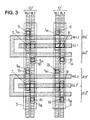
- FIG. 3 shows a layout of an exemplary portion of a semiconductor array according to a preferred embodiment of the present invention.
- a semiconductor array according to Prior Art comprises cells 1 0A , 1 0B , 1 1A , 1 1B , 1 2A , 1 2B , 1 3A , 1 3B .
- Each cell is coupled to a number of control lines.
- the cell 1 0A is coupled to a word line WL1, a source line SL1 and to a bit line BL0.
- Bit lines BL0, BL1, BL2, BL3 extend over corresponding columns C0, C1, C2, C3, whereas word lines WL0, WL1, WL2, WL3 and source lines SL0, SL1, SL2 extend over corresponding rows R1, R2, R3, R4. Active areas 2 0 , 2 1 , 2 2 , 2 3 extend over corresponding columns C0, C1, C2, C3.
- Each cell shares its source terminal with another cell in the same column.
- the cells 1 0A and 1 0B share a same source terminal, i.e. a single trace (not represented) is provided for the shared source terminal.
- the cells 1 0A and 1 0B are subsequently connected to a same source line SL1.
- the cells 1 0A and 1 0B are thus coupled to a same source line SL1 and a same bit line BL0.
- Source lines SL0, SL1, SL2 and bit lines BL0, BL1, BL2, BL3 are selection lines that allow selecting a cell, whereas word lines WL0, WL1, WL2, WL3 are access lines that allow reading/writing the content of a selected cell.
- the cells are written or read word by word, each word being four cells long in this example.
- the source line SL1 is set, the bit lines BL0, BL1, BL2, BL3 are set one after the other, and the value of the word line WL1 changes according to the voltage at the cell of the word corresponding to the currently set bit line. If this word is written, the word line WL1 takes the desired value for each cell selected by the currently set bit line.
- the voltages stored at adjacent cells 1 0B , 1 1B , 1 2B , 1 3B may be affected by the voltages at the source line SL1 and at the corresponding bit line BL0, BL1, BL2, BL3.
- FIG. 2 shows an example of a semiconductor array according to an embodiment of the invention.
- the array is a memory array.
- the semiconductor array may be a PLA.
- the memory array comprises a matrix of cells 1 0A , 1 0B , 1 1A , 1 1B , 1 2A , 1 2B , 1 3A , 1 3B , and a plurality of control lines BL0, BL1, BL2, BL3, SL1, SL1', WL1, WL2.
- Each cell comprises a number of elements depending on the kind of memory array.
- the memory array may be a 1T DRAM, and each cell may comprise a single transistor.
- Each cell 1 0A , 1 0B , 1 1A , 1 1B , 1 2A , 1 2B , 1 3A , 1 3B may be selected by means of corresponding selection lines BL0, BL1, BL2, BL3, SL1, SL1', and may be written or read by means of a corresponding access line WL1, WL2.
- Selection lines comprise bit lines BL0, BL1, BL2, BL3 connected to drain terminals traces 9, 15, 11, 13, 10, 16, 12, 14, of the corresponding cells 1 0A , 1 0B , 1 1A , 1 1B , 1 2A , 1 2B , 1 3A , 1 3B , and source lines connected to source terminals traces 5, 7, 6, 8, 5', 7', 6', 8' of the corresponding cells 1 0A , 1 0B , 1 1A , 1 1B , 1 2A , 1 2B , 1 3A , 1 3B .
- Access lines comprise word lines WL1, WL2 connected to gate terminals of the corresponding cells 1 0A , 1 0B , 1 1A , 1 1B , 1 2A , 1 2B , 1 3A , 1 3B .
- Each bit line BL0, BL1, BL2, BL3 is connected to cells of a single column C0', C1', each column being delimited by an active area 3, 4.
- Each source line SL1, SL1' is connected to cells of a plurality of columns C0', C1' and of two rows R2', R2", R3', R3".
- Each word line WL1, WL2 is connected to cells of a plurality of columns C0', C1' and of two rows R2', R2", R3', R3". That is, each source line SL1, SL1' is connected to cells of an n x m block of cells, n being both greater or equal to two and m being also greater or equal to two.
- Each word line WL1, WL2 is connected to the cells of the n x m block of cells.
- each source line and each word line would extend over 16 columns.
- C1' corresponds two bit lines BL0, BL1, BL2, BL3.
- the source lines and the word lines may extend over more than two rows. However, in this latter case, more than two bit lines have to be formed per column.
- Each cell is coupled to a word line, a source line and a bit line, like in Prior Art.
- the source lines and word lines are arranged so as to allow a better electrical control than in the prior art.
- A is the area of a section of the wire, i.e. A varies with the width of the control line in our example.
- the length of the path crossed by the electrons is indeed substantially two times shorter than in Prior Art.
- the resistance encountered is thus substantially two times shorter, which allows a better electrical control than in Prior Art.
- the source lines and the word lines are arranged to as to provide an even smaller resistance.
- the source lines SL1, SL1' and word lines WL1, WL2 are coupled with cells of two columns C0', C1', and two rows R2', R2", R2', R3". Furthermore, each cell 1 0A , 1 1A , 1 0B , 1 1B of the two rows shares one of its terminals with a distinct cell in another one of the two rows and in the same column. For example, a same source terminal trace 5 is used as source terminal for both cells 1 0A and 1 2A . Similarly, a same source terminal trace 6, 7, 8 is used as source terminal respectively for the pairs of cells 1 1A and 1 3A , 1 0B and 1 2B , 1 1B and 1 3B .
- Such a terminal share allows saving area.
- the shape of the source lines SL1, SL1' mat be relatively simple, as shown in FIG. 3 .
- the resistance of the source line is hence relatively small, thus allowing a better electrical control.
- the cells that shares a same terminal may be relatively close to each other, that is the word lines WL1, WL2 may also be relatively short.
- the resistance of the word lines WL1, WL2 may hence be relatively small.
- the cells are floating body cells.
- the cells may for example be realized in a SOI technology.
- the cell 1 2A may have its gate voltage lowered by a few percents upon a reading/writing of the cell 1 0A .
- the cells 1 0A and 1 2A belong to same word, i.e. the cell 1 2A is also attended to be read/written. The disturbing hence causes only little damage.
Abstract
Description
- The present invention relates to semiconductor arrays.
- Although the present description focuses mainly on floating body memory arrays, the possible fields of application of the invention are manifold. For example, embodiments of the invention also include CMOS memory arrays, or even programmable logic arrays such as PLAs.
- A memory array comprises a plurality of memory cells, or cells, and is organized into rows and columns of such cells. A column extends over the matrix in a vertical direction, whereas a row extends over the matrix in a horizontal direction. The cell that lies at the ith row and the jth column is called the i,j cell. The cells of a same column have a same j index, the i index varying from 1 to the number of rows of the matrix. The cells of a same row have a same i index, the j index varying from 1 to the number of columns of the matrix.
- Each cell may comprise one or more storing elements, e.g. transistor(s) and/or capacitor(s). Each cell may be coupled to a number of control lines, e.g. one source line, one word line and one bit line. The control lines are conductive, e.g. metallic lines, which are typically connected to one or more transistor(s) of the cell, via their source, gate or drain terminals for example.
- Addressable bit lines may be coupled to the cells in a corresponding column of cells, and the cells in any row of cells may be coupled to a corresponding pair of addressable word and source lines. The control lines hence allow selecting any cell of the array and reading from or writing to the selected cell.
- The words may typically comprise 8, 16, 32, 64, 128 or 256 bits, i.e. each word line is coupled to 8, 16, 32, 64, 128 or 256 cells respectively. As the number of cells in a row increases, the electrons in the word line or in the source line have to move over an increasingly long path. Furthermore, the dimensions of the semiconductor array tend to shrink, i.e. the section of the control line crossed by the electrons becomes smaller and smaller. The cells may therefore be relatively difficult to control in read and/or write mode.
- The present invention aims at improving the electrical control of the cells.
- In a first aspect, the invention provides a semiconductor array comprising a matrix of cells, and a plurality of control lines, each cell being coupled to a number of control lines allowing to select and to read data from or write data into the cell. The matrix is arranged in rows and columns of cells. At least one of the control lines is coupled to cells of a plurality of columns and of at least two rows of the matrix.
- In such a block arrangement, this control line may be arranged so as to facilitate the moving of the electrons, thus allowing better electrical control of the coupled cells.
- Typically, the number of control lines to which each cell is coupled comprises at least one selection line adapted to select the cell, and at least one access line adapted to read/write data from/into the cell.
- The semiconductor array may for example comprise a memory array, or a logic array, e.g. programmable logic array (PLA), programmable array logic (PAL), field programmable gate array (FPGA), erasable programmable logic device (EPLD) etc.
- The memory array may for example comprise a 1T DRAM, a 1T/1C DRAM or a 6T SRAM, the letters T and C referring to the number of transistors and capacitors, respectively, in one memory cell. The memory array may also comprise a flash memory, each cell of which comprising a transistor having a double gate. The memory array may also comprise a charge memory, each cell of which comprising a transistor and a variable resistor.
- The semiconductor array may be realized using any technology, e.g. complementary metal-oxyde-semiconductor (CMOS) technology, silicon on insulator (SOI) technology, Silicon on Nothing (SON) technology, a FinFET technology etc.
- Some technologies, e.g. SOI and SON technologies, allow insulating components of the cells, such as transistors, thus allowing avoiding insulation regions, e.g. shallow trench isolation (STI) regions. For example, the body of a SOI transistor, i.e. the region between a source region and a drain region, is electrically floating, and no specific insulation region is needed to achieve insulation. Such floating body cells allow higher densities and smaller areas.
- With the present invention, at least one of the control lines is coupled to cells of a plurality of columns and of at least two rows of the matrix. Advantageously, at least one cell of the at least two rows shares one of its terminals with a distinct cell in the another one of the at least two rows and in the same column, thus allowing to save silicon area.
- By "sharing a terminal", it is not only meant that the terminals of the two cells are electrically connected, but also that a single trace without insulating region is used for the shared terminal in the layout of the array.
- Alternatively, no cell in the at least two rows shares one of its terminals with a distinct cell in the another one of these two rows and in the same column. That is, for each cell in these two rows, an insulating region is provided between this cell and any adjacent cell.
- In prior art memory arrays, source terminals are shared between two cells within a same column. The cells sharing a same source terminal are coupled to a same bit line connected to their drain terminals, and to distinct word lines. The gate terminal of each cell is connected to a corresponding word line. In a prior art floating body memory array, addressing a determined cell may cause possible disturbs on the adjacent cell that shares its source terminal with the addressed cell. For example, when 2V is applied to the drain terminal of the addressed cell, the voltage at the body of the adjacent cell may rise up to substantially 0,6V if the gate and source terminals of the unselected cell are at 0V, as desired for operating with minimum power and high speed.
- Typically, each writing or reading may cause a few percents modification to the voltage stored in the cell adjacent to the cell which is read or written. After a number of reading/writing cycles, the values stored in the adjacent cell may turn out to be irrelevant.
- Advantageously, two distinct selection lines are respectively coupled to the at least one cell and to the distinct cell that share a same terminal, i.e. there is a selection line that is not coupled to both cells. In the prior art, two cells sharing a source terminal have all their selection lines, e.g. source line and bit line, in common. When a word of a number of cells, e.g. 32 cells, is to be read/written, 32 bit lines are set so as to select the 32 cells. For each cell that is read or written, the adjacent cell that is disturbed is coupled to a same bit line and to a same source line. The disturbed cells hence do not belong to the group (word) of cells which is read or written.
- If there is a selection line that is not coupled to both cells, it may be possible to read/write data from/into a number of cells without disturbing the cells of others words. Indeed, the adjacent cells that are disturbed may belong to the word that is being read/written, i.e. the consequences of a possible disturbing are very low.
- In a further aspect, the invention provides a method for manufacturing a semiconductor array comprising a matrix of cells, the method comprising providing a plurality of control lines such that each cell is coupled to a number of control lines allowing to select and read/write said cell and such that at least one of said control lines is coupled to cells of a plurality of columns and of at least two rows of the matrix.
- These and other aspects of the invention will be apparent from and elucidated with reference to the embodiments described hereinafter.
-
FIG. 1 shows a layout of an example of a portion of a semiconductor array according to Prior Art. -
FIG.2 shows a layout of an exemplary portion of a semiconductor array according to an embodiment of the present invention. -
FIG. 3 shows a layout of an exemplary portion of a semiconductor array according to a preferred embodiment of the present invention. - In all the figures, the same references denote similar or substantially similar elements.
- As shown in
FIG.1 , a semiconductor array according to Prior Art comprisescells cell 10A is coupled to a word line WL1, a source line SL1 and to a bit line BL0. - Bit lines BL0, BL1, BL2, BL3 extend over corresponding columns C0, C1, C2, C3, whereas word lines WL0, WL1, WL2, WL3 and source lines SL0, SL1, SL2 extend over corresponding rows R1, R2, R3, R4. Active areas 20, 21, 22, 23 extend over corresponding columns C0, C1, C2, C3.
- Each cell shares its source terminal with another cell in the same column. For example, the
cells cells cells - Source lines SL0, SL1, SL2 and bit lines BL0, BL1, BL2, BL3 are selection lines that allow selecting a cell, whereas word lines WL0, WL1, WL2, WL3 are access lines that allow reading/writing the content of a selected cell.
- The cells are written or read word by word, each word being four cells long in this example. When the word comprising the
cells - During such read/write operations, the voltages stored at
adjacent cells -
FIG. 2 shows an example of a semiconductor array according to an embodiment of the invention. - In this embodiment, the array is a memory array. In an alternative embodiment (not represented), the semiconductor array may be a PLA.
- The memory array comprises a matrix of
cells - Each cell comprises a number of elements depending on the kind of memory array. For example, the memory array may be a 1T DRAM, and each cell may comprise a single transistor.
- Each
cell - Selection lines comprise bit lines BL0, BL1, BL2, BL3 connected to drain terminals traces 9, 15, 11, 13, 10, 16, 12, 14, of the corresponding
cells cells - Access lines comprise word lines WL1, WL2 connected to gate terminals of the corresponding
cells - Each bit line BL0, BL1, BL2, BL3 is connected to cells of a single column C0', C1', each column being delimited by an
active area - Each source line SL1, SL1', is connected to cells of a plurality of columns C0', C1' and of two rows R2', R2", R3', R3". Each word line WL1, WL2 is connected to cells of a plurality of columns C0', C1' and of two rows R2', R2", R3', R3". That is, each source line SL1, SL1' is connected to cells of an n x m block of cells, n being both greater or equal to two and m being also greater or equal to two. Each word line WL1, WL2 is connected to the cells of the n x m block of cells.
- In this example, each word is four cells long, that is each source line and each word line extends over two columns C0', C1'. That is, n=2 and m=2.
- For a 32 cells long word, as long as the source lines and the word lines also extend over two rows, each source line and each word line would extend over 16 columns.
- To each column C0', C1' corresponds two bit lines BL0, BL1, BL2, BL3. One may note that the source lines and the word lines may extend over more than two rows. However, in this latter case, more than two bit lines have to be formed per column.
- Each cell is coupled to a word line, a source line and a bit line, like in Prior Art.
- The source lines and word lines are arranged so as to allow a better electrical control than in the prior art.
- The resistance R of a wire may be expressed as:

- Wherein
- p is the resistivity of the material of the wire,
- L is the length of the path crossed by the electrons,
- And A is the area of a section of the wire, i.e. A varies with the width of the control line in our example.
- In the embodiment illustrated in
FIG.2 , the length of the path crossed by the electrons is indeed substantially two times shorter than in Prior Art. The resistance encountered is thus substantially two times shorter, which allows a better electrical control than in Prior Art. - In the embodiment illustrated in
FIG.3 , the source lines and the word lines are arranged to as to provide an even smaller resistance. - Like in
FIG. 2 , the source lines SL1, SL1' and word lines WL1, WL2 are coupled with cells of two columns C0', C1', and two rows R2', R2", R2', R3". Furthermore, eachcell terminal trace 5 is used as source terminal for bothcells terminal trace cells - Such a terminal share allows saving area. Also, the shape of the source lines SL1, SL1' mat be relatively simple, as shown in
FIG. 3 . The resistance of the source line is hence relatively small, thus allowing a better electrical control. - The cells that shares a same terminal may be relatively close to each other, that is the word lines WL1, WL2 may also be relatively short. The resistance of the word lines WL1, WL2 may hence be relatively small.
- In this embodiment, the cells are floating body cells. The cells may for example be realized in a SOI technology.
- One may subsequently expect that the cells sharing a same terminal with the cells that are read/written be disturbed by the reading/writing operation. For example, the
cell 12A may have its gate voltage lowered by a few percents upon a reading/writing of thecell 10A. However, thecells cell 12A is also attended to be read/written. The disturbing hence causes only little damage.
Claims (8)
- A semiconductor array comprising
a matrix of cells (10A, 10B, 11A, 11B, 12A, 12B, 13A, 13B), the matrix being arranged in rows (R2', R2", R3', R3") and columns (C0', C1') of cells,
a plurality of control lines (BL0, BL1, BL2, BL3, SL1, SL1', WL1, WL2), each cell being coupled to a number of control lines allowing to select and read/write said cell,
at least one of said control lines is coupled to cells of a plurality of columns and of at least two rows of the matrix. - The semiconductor array of Claim 1, the array comprising a memory array.
- The semiconductor array of any one of claims 1 to 2, wherein the cells are floating body cells.
- The semiconductor array of any one of the preceding claims, said array being realised in a SOI technology.
- The semiconductor array of any one of claims 1 to 3, said array being realised in a SON technology.
- The semiconductor array of any one of the preceding claims, wherein
at least one cell (10A, 10B, 11A, 11B, 12A, 12B, 13A, 13B) of said at least two rows (R2', R2", R3', R3") shares one of its terminals with a distinct cell in another one of said at least two rows and in the same column. - The semiconductor array of claim 6, wherein
the number of control lines to which is coupled each cell (10A, 10B, 11A, 11B, 12A, 12B, 13A, 13B) comprises at least one selection line (BL0, BL1, BL2, BL3, SL1, SL1') adapted to select said cell, and at least one access line (WL1, WL2) adapted to read/write said cell,
two distinct selection lines are respectively coupled to the at least one cell and to the distinct cell that share a same terminal. - A method for manufacturing a semiconductor array comprising a matrix of cells (10A, 10B, 11A, 11B, 12A, 12B, 13A, 13B), the matrix being arranged in rows (R2', R2", R3', R3") and columns (C0', C1') of cells, the method comprising
providing a plurality of control lines (BL0, BL1, BL2, BL3, SL1, SL1', WL1, WL2) such that each cell is coupled to a number of control lines allowing to select and read/write said cell and such that at least one of said control lines is coupled to cells of a plurality of columns and of at least two rows of the matrix.
Priority Applications (2)
| Application Number | Priority Date | Filing Date | Title |
|---|---|---|---|
| EP07301083A EP2015362A1 (en) | 2007-06-04 | 2007-06-04 | Semiconductor array and manufacturing method thereof |
| US12/130,918 US7817466B2 (en) | 2007-06-04 | 2008-05-30 | Semiconductor array including a matrix of cells and a method of making a semiconductor array having a matrix of cells |
Applications Claiming Priority (1)
| Application Number | Priority Date | Filing Date | Title |
|---|---|---|---|
| EP07301083A EP2015362A1 (en) | 2007-06-04 | 2007-06-04 | Semiconductor array and manufacturing method thereof |
Publications (1)
| Publication Number | Publication Date |
|---|---|
| EP2015362A1 true EP2015362A1 (en) | 2009-01-14 |
Family
ID=38626377
Family Applications (1)
| Application Number | Title | Priority Date | Filing Date |
|---|---|---|---|
| EP07301083A Withdrawn EP2015362A1 (en) | 2007-06-04 | 2007-06-04 | Semiconductor array and manufacturing method thereof |
Country Status (2)
| Country | Link |
|---|---|
| US (1) | US7817466B2 (en) |
| EP (1) | EP2015362A1 (en) |
Families Citing this family (56)
| Publication number | Priority date | Publication date | Assignee | Title |
|---|---|---|---|---|
| US7606066B2 (en) | 2005-09-07 | 2009-10-20 | Innovative Silicon Isi Sa | Memory cell and memory cell array having an electrically floating body transistor, and methods of operating same |
| US7492632B2 (en) | 2006-04-07 | 2009-02-17 | Innovative Silicon Isi Sa | Memory array having a programmable word length, and method of operating same |
| WO2007128738A1 (en) * | 2006-05-02 | 2007-11-15 | Innovative Silicon Sa | Semiconductor memory cell and array using punch-through to program and read same |
| US8069377B2 (en) * | 2006-06-26 | 2011-11-29 | Micron Technology, Inc. | Integrated circuit having memory array including ECC and column redundancy and method of operating the same |
| US8264041B2 (en) * | 2007-01-26 | 2012-09-11 | Micron Technology, Inc. | Semiconductor device with electrically floating body |
| WO2009031052A2 (en) | 2007-03-29 | 2009-03-12 | Innovative Silicon S.A. | Zero-capacitor (floating body) random access memory circuits with polycide word lines and manufacturing methods therefor |
| US8064274B2 (en) | 2007-05-30 | 2011-11-22 | Micron Technology, Inc. | Integrated circuit having voltage generation circuitry for memory cell array, and method of operating and/or controlling same |
| US8085594B2 (en) * | 2007-06-01 | 2011-12-27 | Micron Technology, Inc. | Reading technique for memory cell with electrically floating body transistor |
| US8194487B2 (en) | 2007-09-17 | 2012-06-05 | Micron Technology, Inc. | Refreshing data of memory cells with electrically floating body transistors |
| US8536628B2 (en) | 2007-11-29 | 2013-09-17 | Micron Technology, Inc. | Integrated circuit having memory cell array including barriers, and method of manufacturing same |
| US8349662B2 (en) * | 2007-12-11 | 2013-01-08 | Micron Technology, Inc. | Integrated circuit having memory cell array, and method of manufacturing same |
| US8773933B2 (en) | 2012-03-16 | 2014-07-08 | Micron Technology, Inc. | Techniques for accessing memory cells |
| US8014195B2 (en) | 2008-02-06 | 2011-09-06 | Micron Technology, Inc. | Single transistor memory cell |
| US8189376B2 (en) * | 2008-02-08 | 2012-05-29 | Micron Technology, Inc. | Integrated circuit having memory cells including gate material having high work function, and method of manufacturing same |
| US7957206B2 (en) * | 2008-04-04 | 2011-06-07 | Micron Technology, Inc. | Read circuitry for an integrated circuit having memory cells and/or a memory cell array, and method of operating same |
| US7947543B2 (en) * | 2008-09-25 | 2011-05-24 | Micron Technology, Inc. | Recessed gate silicon-on-insulator floating body device with self-aligned lateral isolation |
| US7933140B2 (en) * | 2008-10-02 | 2011-04-26 | Micron Technology, Inc. | Techniques for reducing a voltage swing |
| US7924630B2 (en) | 2008-10-15 | 2011-04-12 | Micron Technology, Inc. | Techniques for simultaneously driving a plurality of source lines |
| US8223574B2 (en) * | 2008-11-05 | 2012-07-17 | Micron Technology, Inc. | Techniques for block refreshing a semiconductor memory device |
| US8213226B2 (en) | 2008-12-05 | 2012-07-03 | Micron Technology, Inc. | Vertical transistor memory cell and array |
| US8319294B2 (en) * | 2009-02-18 | 2012-11-27 | Micron Technology, Inc. | Techniques for providing a source line plane |
| US8710566B2 (en) | 2009-03-04 | 2014-04-29 | Micron Technology, Inc. | Techniques for forming a contact to a buried diffusion layer in a semiconductor memory device |
| US8748959B2 (en) * | 2009-03-31 | 2014-06-10 | Micron Technology, Inc. | Semiconductor memory device |
| US8139418B2 (en) * | 2009-04-27 | 2012-03-20 | Micron Technology, Inc. | Techniques for controlling a direct injection semiconductor memory device |
| US8508994B2 (en) * | 2009-04-30 | 2013-08-13 | Micron Technology, Inc. | Semiconductor device with floating gate and electrically floating body |
| US8498157B2 (en) * | 2009-05-22 | 2013-07-30 | Micron Technology, Inc. | Techniques for providing a direct injection semiconductor memory device |
| US8537610B2 (en) | 2009-07-10 | 2013-09-17 | Micron Technology, Inc. | Techniques for providing a semiconductor memory device |
| US9076543B2 (en) | 2009-07-27 | 2015-07-07 | Micron Technology, Inc. | Techniques for providing a direct injection semiconductor memory device |
| US20110054468A1 (en) * | 2009-09-01 | 2011-03-03 | Tyco Healthcare Group Lp | Apparatus for Performing an Electrosurgical Procedure |
| US8199595B2 (en) * | 2009-09-04 | 2012-06-12 | Micron Technology, Inc. | Techniques for sensing a semiconductor memory device |
| EP2320454A1 (en) * | 2009-11-05 | 2011-05-11 | S.O.I.Tec Silicon on Insulator Technologies | Substrate holder and clipping device |
| US8174881B2 (en) | 2009-11-24 | 2012-05-08 | Micron Technology, Inc. | Techniques for reducing disturbance in a semiconductor device |
| FR2953641B1 (en) * | 2009-12-08 | 2012-02-10 | S O I Tec Silicon On Insulator Tech | HOMOGENEOUS TRANSISTOR CIRCUIT ON SEOI WITH REAR CONTROL CHANNEL BURED UNDER THE INSULATING LAYER |
| US8508289B2 (en) * | 2009-12-08 | 2013-08-13 | Soitec | Data-path cell on an SeOI substrate with a back control gate beneath the insulating layer |
| FR2953643B1 (en) * | 2009-12-08 | 2012-07-27 | Soitec Silicon On Insulator | MEMORY CELL FLASH ON SEOI HAVING A SECOND CHECK GRID ENTERREE UNDER THE INSULATING LAYER |
| FR2953636B1 (en) * | 2009-12-08 | 2012-02-10 | Soitec Silicon On Insulator | METHOD FOR CONTROLLING A DRAM MEMORY CELL ON SEOI HAVING A SECOND BURST CONTROL GRID UNDER THE INSULATING LAYER |
| FR2957193B1 (en) | 2010-03-03 | 2012-04-20 | Soitec Silicon On Insulator | SEOI SUBSTRATE DATA PATH CELL WITH REAR CONTROL GRID BURED UNDER THE INSULATING LAYER |
| US8310893B2 (en) | 2009-12-16 | 2012-11-13 | Micron Technology, Inc. | Techniques for reducing impact of array disturbs in a semiconductor memory device |
| FR2955204B1 (en) * | 2010-01-14 | 2012-07-20 | Soitec Silicon On Insulator | DRAM MEMORY CELL HAVING A VERTICAL BIPOLAR INJECTOR |
| FR2955203B1 (en) | 2010-01-14 | 2012-03-23 | Soitec Silicon On Insulator | MEMORY CELL WITH THE CHANNEL CROSSING A DIELECTRIC LAYER ENTERREE |
| FR2955195B1 (en) * | 2010-01-14 | 2012-03-09 | Soitec Silicon On Insulator | DEVICE FOR COMPARING DATA IN A MEMORY ADDRESSABLE BY CONTENT ON SEOI |
| FR2955200B1 (en) | 2010-01-14 | 2012-07-20 | Soitec Silicon On Insulator | DEVICE AND MANUFACTURING METHOD HAVING CONTACT BETWEEN SEMICONDUCTOR REGIONS THROUGH AN INSULATED INSULATED LAYER |
| US8416636B2 (en) | 2010-02-12 | 2013-04-09 | Micron Technology, Inc. | Techniques for controlling a semiconductor memory device |
| US8411513B2 (en) * | 2010-03-04 | 2013-04-02 | Micron Technology, Inc. | Techniques for providing a semiconductor memory device having hierarchical bit lines |
| US8576631B2 (en) * | 2010-03-04 | 2013-11-05 | Micron Technology, Inc. | Techniques for sensing a semiconductor memory device |
| US8369177B2 (en) * | 2010-03-05 | 2013-02-05 | Micron Technology, Inc. | Techniques for reading from and/or writing to a semiconductor memory device |
| FR2957186B1 (en) * | 2010-03-08 | 2012-09-28 | Soitec Silicon On Insulator | MEMORY CELL OF SRAM TYPE |
| FR2957449B1 (en) * | 2010-03-11 | 2022-07-15 | S O I Tec Silicon On Insulator Tech | READOUT MICRO-AMPLIFIER FOR MEMORY |
| WO2011115893A2 (en) | 2010-03-15 | 2011-09-22 | Micron Technology, Inc. | Techniques for providing a semiconductor memory device |
| FR2958441B1 (en) | 2010-04-02 | 2012-07-13 | Soitec Silicon On Insulator | PSEUDO-INVERTER CIRCUIT ON SEOI |
| EP2378549A1 (en) | 2010-04-06 | 2011-10-19 | S.O.I.Tec Silicon on Insulator Technologies | Method for manufacturing a semiconductor substrate |
| EP2381470B1 (en) | 2010-04-22 | 2012-08-22 | Soitec | Semiconductor device comprising a field-effect transistor in a silicon-on-insulator structure |
| US8411524B2 (en) | 2010-05-06 | 2013-04-02 | Micron Technology, Inc. | Techniques for refreshing a semiconductor memory device |
| US8531878B2 (en) | 2011-05-17 | 2013-09-10 | Micron Technology, Inc. | Techniques for providing a semiconductor memory device |
| US9559216B2 (en) | 2011-06-06 | 2017-01-31 | Micron Technology, Inc. | Semiconductor memory device and method for biasing same |
| US9793378B2 (en) | 2013-05-31 | 2017-10-17 | Stmicroelectronics, Inc. | Fin field effect transistor device with reduced overlap capacitance and enhanced mechanical stability |
Citations (7)
| Publication number | Priority date | Publication date | Assignee | Title |
|---|---|---|---|---|
| US5821592A (en) * | 1997-06-30 | 1998-10-13 | Siemens Aktiengesellschaft | Dynamic random access memory arrays and methods therefor |
| US5825688A (en) * | 1994-07-26 | 1998-10-20 | Mitsubishi Denki Kabushiki Kaisha | Non-volatile semiconductor storage apparatus |
| US6226218B1 (en) * | 1999-04-23 | 2001-05-01 | Samsung Electronics Co., Ltd. | Row decoder driver for semiconductor memory device |
| US20040190350A1 (en) * | 2003-03-31 | 2004-09-30 | Osamu Wada | Semiconductor memory device |
| US20050104232A1 (en) * | 2003-11-14 | 2005-05-19 | Chung-Chin Shih | [memory device and fabrication method thereof] |
| US20050280001A1 (en) * | 2004-06-22 | 2005-12-22 | Chang Peter L | Memory cell using silicon carbide |
| EP1772872A1 (en) * | 2005-10-06 | 2007-04-11 | Seiko Epson Corporation | Semiconductor memory device and electronic apparatus |
Family Cites Families (6)
| Publication number | Priority date | Publication date | Assignee | Title |
|---|---|---|---|---|
| TWI230392B (en) | 2001-06-18 | 2005-04-01 | Innovative Silicon Sa | Semiconductor device |
| US20040228168A1 (en) * | 2003-05-13 | 2004-11-18 | Richard Ferrant | Semiconductor memory device and method of operating same |
| US7301803B2 (en) | 2004-12-22 | 2007-11-27 | Innovative Silicon S.A. | Bipolar reading technique for a memory cell having an electrically floating body transistor |
| US7606066B2 (en) * | 2005-09-07 | 2009-10-20 | Innovative Silicon Isi Sa | Memory cell and memory cell array having an electrically floating body transistor, and methods of operating same |
| US7606057B2 (en) * | 2006-05-31 | 2009-10-20 | Arm Limited | Metal line layout in a memory cell |
| KR101043980B1 (en) * | 2006-09-29 | 2011-06-24 | 후지쯔 세미컨덕터 가부시키가이샤 | Nonvolatile semiconductor storage apparatus, reading method thereof, writing method thereof and erasing method thereof |
-
2007
- 2007-06-04 EP EP07301083A patent/EP2015362A1/en not_active Withdrawn
-
2008
- 2008-05-30 US US12/130,918 patent/US7817466B2/en active Active
Patent Citations (7)
| Publication number | Priority date | Publication date | Assignee | Title |
|---|---|---|---|---|
| US5825688A (en) * | 1994-07-26 | 1998-10-20 | Mitsubishi Denki Kabushiki Kaisha | Non-volatile semiconductor storage apparatus |
| US5821592A (en) * | 1997-06-30 | 1998-10-13 | Siemens Aktiengesellschaft | Dynamic random access memory arrays and methods therefor |
| US6226218B1 (en) * | 1999-04-23 | 2001-05-01 | Samsung Electronics Co., Ltd. | Row decoder driver for semiconductor memory device |
| US20040190350A1 (en) * | 2003-03-31 | 2004-09-30 | Osamu Wada | Semiconductor memory device |
| US20050104232A1 (en) * | 2003-11-14 | 2005-05-19 | Chung-Chin Shih | [memory device and fabrication method thereof] |
| US20050280001A1 (en) * | 2004-06-22 | 2005-12-22 | Chang Peter L | Memory cell using silicon carbide |
| EP1772872A1 (en) * | 2005-10-06 | 2007-04-11 | Seiko Epson Corporation | Semiconductor memory device and electronic apparatus |
Also Published As
| Publication number | Publication date |
|---|---|
| US20090086535A1 (en) | 2009-04-02 |
| US7817466B2 (en) | 2010-10-19 |
Similar Documents
| Publication | Publication Date | Title |
|---|---|---|
| EP2015362A1 (en) | Semiconductor array and manufacturing method thereof | |
| CN112700812B (en) | Three-dimensional memory device with reduced disturb and programming method | |
| US6657894B2 (en) | Apparatus and method for programming virtual ground nonvolatile memory cell array without disturbing adjacent cells | |
| US10395736B2 (en) | Resistive random access memory device | |
| CN102332300B (en) | Semiconductor memory device | |
| CN102349112B (en) | Memory device having improved programming operation | |
| KR101088954B1 (en) | Programmable non-volatile memory | |
| US6028784A (en) | Ferroelectric memory device having compact memory cell array | |
| US8836007B2 (en) | Programmable logic switch | |
| US7660148B2 (en) | Nonvolatile memory device and method to control the same | |
| US4425632A (en) | Nonvolatile semiconductor memory device | |
| CN105308751A (en) | Apparatuses having a ferroelectric field-effect transistor memory array and related method | |
| US11289145B2 (en) | Memory cell, memory cell arrangement, and methods thereof | |
| CN101454842A (en) | A method for programming and erasing an array of nmos eeprom cells that minimize bit disturbances and voltage withstand requirements for the memory array and supporting circuits | |
| US7505325B2 (en) | Low voltage low capacitance flash memory array | |
| US11527551B2 (en) | Memory cell arrangements and methods thereof | |
| US7126185B2 (en) | Charge trap insulator memory device | |
| KR102575943B1 (en) | One-time-programmable memory | |
| US20070279967A1 (en) | High density magnetic memory cell layout for spin transfer torque magnetic memories utilizing donut shaped transistors | |
| KR20130123904A (en) | Semiconductor memory device | |
| US11443792B1 (en) | Memory cell, memory cell arrangement, and methods thereof | |
| TWI780658B (en) | Memory circuit and method of operating same | |
| US7352605B2 (en) | Nonvolatile ferroelectric memory device and method thereof | |
| US7366027B2 (en) | Method and apparatus for erasing memory | |
| KR20040070218A (en) | A device and method to read a 2-transistor flash memory cell |
Legal Events
| Date | Code | Title | Description |
|---|---|---|---|
| PUAI | Public reference made under article 153(3) epc to a published international application that has entered the european phase |
Free format text: ORIGINAL CODE: 0009012 |
|
| AK | Designated contracting states |
Kind code of ref document: A1 Designated state(s): AT BE BG CH CY CZ DE DK EE ES FI FR GB GR HU IE IS IT LI LT LU LV MC MT NL PL PT RO SE SI SK TR |
|
| AX | Request for extension of the european patent |
Extension state: AL BA HR MK RS |
|
| 17P | Request for examination filed |
Effective date: 20090513 |
|
| 17Q | First examination report despatched |
Effective date: 20090710 |
|
| AKX | Designation fees paid |
Designated state(s): AT BE BG CH CY CZ DE DK EE ES FI FR GB GR HU IE IS IT LI LT LU LV MC MT NL PL PT RO SE SI SK TR |
|
| RAP1 | Party data changed (applicant data changed or rights of an application transferred) |
Owner name: FREESCALE SEMICONDUCTOR, INC. Owner name: STMICROELECTRONICS (CROLLES 2) SAS |
|
| STAA | Information on the status of an ep patent application or granted ep patent |
Free format text: STATUS: THE APPLICATION IS DEEMED TO BE WITHDRAWN |
|
| 18D | Application deemed to be withdrawn |
Effective date: 20140103 |