EP2015294A1 - Producing method of suspension board with circuit - Google Patents
Producing method of suspension board with circuit Download PDFInfo
- Publication number
- EP2015294A1 EP2015294A1 EP20080159998 EP08159998A EP2015294A1 EP 2015294 A1 EP2015294 A1 EP 2015294A1 EP 20080159998 EP20080159998 EP 20080159998 EP 08159998 A EP08159998 A EP 08159998A EP 2015294 A1 EP2015294 A1 EP 2015294A1
- Authority
- EP
- European Patent Office
- Prior art keywords
- mark
- layer
- conductive pattern
- seed film
- exposed
- Prior art date
- Legal status (The legal status is an assumption and is not a legal conclusion. Google has not performed a legal analysis and makes no representation as to the accuracy of the status listed.)
- Withdrawn
Links
Images







Classifications
-
- G—PHYSICS
- G11—INFORMATION STORAGE
- G11B—INFORMATION STORAGE BASED ON RELATIVE MOVEMENT BETWEEN RECORD CARRIER AND TRANSDUCER
- G11B5/00—Recording by magnetisation or demagnetisation of a record carrier; Reproducing by magnetic means; Record carriers therefor
- G11B5/48—Disposition or mounting of heads or head supports relative to record carriers ; arrangements of heads, e.g. for scanning the record carrier to increase the relative speed
- G11B5/4806—Disposition or mounting of heads or head supports relative to record carriers ; arrangements of heads, e.g. for scanning the record carrier to increase the relative speed specially adapted for disk drive assemblies, e.g. assembly prior to operation, hard or flexible disk drives
- G11B5/484—Integrated arm assemblies, e.g. formed by material deposition or by etching from single piece of metal or by lamination of materials forming a single arm/suspension/head unit
-
- H—ELECTRICITY
- H05—ELECTRIC TECHNIQUES NOT OTHERWISE PROVIDED FOR
- H05K—PRINTED CIRCUITS; CASINGS OR CONSTRUCTIONAL DETAILS OF ELECTRIC APPARATUS; MANUFACTURE OF ASSEMBLAGES OF ELECTRICAL COMPONENTS
- H05K1/00—Printed circuits
- H05K1/02—Details
- H05K1/0266—Marks, test patterns or identification means
- H05K1/0269—Marks, test patterns or identification means for visual or optical inspection
-
- H—ELECTRICITY
- H05—ELECTRIC TECHNIQUES NOT OTHERWISE PROVIDED FOR
- H05K—PRINTED CIRCUITS; CASINGS OR CONSTRUCTIONAL DETAILS OF ELECTRIC APPARATUS; MANUFACTURE OF ASSEMBLAGES OF ELECTRICAL COMPONENTS
- H05K3/00—Apparatus or processes for manufacturing printed circuits
- H05K3/0008—Apparatus or processes for manufacturing printed circuits for aligning or positioning of tools relative to the circuit board
-
- H—ELECTRICITY
- H05—ELECTRIC TECHNIQUES NOT OTHERWISE PROVIDED FOR
- H05K—PRINTED CIRCUITS; CASINGS OR CONSTRUCTIONAL DETAILS OF ELECTRIC APPARATUS; MANUFACTURE OF ASSEMBLAGES OF ELECTRICAL COMPONENTS
- H05K3/00—Apparatus or processes for manufacturing printed circuits
- H05K3/44—Manufacturing insulated metal core circuits or other insulated electrically conductive core circuits
-
- G—PHYSICS
- G11—INFORMATION STORAGE
- G11B—INFORMATION STORAGE BASED ON RELATIVE MOVEMENT BETWEEN RECORD CARRIER AND TRANSDUCER
- G11B5/00—Recording by magnetisation or demagnetisation of a record carrier; Reproducing by magnetic means; Record carriers therefor
- G11B5/48—Disposition or mounting of heads or head supports relative to record carriers ; arrangements of heads, e.g. for scanning the record carrier to increase the relative speed
- G11B5/4806—Disposition or mounting of heads or head supports relative to record carriers ; arrangements of heads, e.g. for scanning the record carrier to increase the relative speed specially adapted for disk drive assemblies, e.g. assembly prior to operation, hard or flexible disk drives
- G11B5/4853—Constructional details of the electrical connection between head and arm
-
- G—PHYSICS
- G11—INFORMATION STORAGE
- G11B—INFORMATION STORAGE BASED ON RELATIVE MOVEMENT BETWEEN RECORD CARRIER AND TRANSDUCER
- G11B5/00—Recording by magnetisation or demagnetisation of a record carrier; Reproducing by magnetic means; Record carriers therefor
- G11B5/48—Disposition or mounting of heads or head supports relative to record carriers ; arrangements of heads, e.g. for scanning the record carrier to increase the relative speed
- G11B5/4806—Disposition or mounting of heads or head supports relative to record carriers ; arrangements of heads, e.g. for scanning the record carrier to increase the relative speed specially adapted for disk drive assemblies, e.g. assembly prior to operation, hard or flexible disk drives
- G11B5/486—Disposition or mounting of heads or head supports relative to record carriers ; arrangements of heads, e.g. for scanning the record carrier to increase the relative speed specially adapted for disk drive assemblies, e.g. assembly prior to operation, hard or flexible disk drives with provision for mounting or arranging electrical conducting means or circuits on or along the arm assembly
-
- H—ELECTRICITY
- H05—ELECTRIC TECHNIQUES NOT OTHERWISE PROVIDED FOR
- H05K—PRINTED CIRCUITS; CASINGS OR CONSTRUCTIONAL DETAILS OF ELECTRIC APPARATUS; MANUFACTURE OF ASSEMBLAGES OF ELECTRICAL COMPONENTS
- H05K2201/00—Indexing scheme relating to printed circuits covered by H05K1/00
- H05K2201/09—Shape and layout
- H05K2201/09009—Substrate related
- H05K2201/09063—Holes or slots in insulating substrate not used for electrical connections
-
- H—ELECTRICITY
- H05—ELECTRIC TECHNIQUES NOT OTHERWISE PROVIDED FOR
- H05K—PRINTED CIRCUITS; CASINGS OR CONSTRUCTIONAL DETAILS OF ELECTRIC APPARATUS; MANUFACTURE OF ASSEMBLAGES OF ELECTRICAL COMPONENTS
- H05K2201/00—Indexing scheme relating to printed circuits covered by H05K1/00
- H05K2201/09—Shape and layout
- H05K2201/09209—Shape and layout details of conductors
- H05K2201/09654—Shape and layout details of conductors covering at least two types of conductors provided for in H05K2201/09218 - H05K2201/095
- H05K2201/0969—Apertured conductors
-
- H—ELECTRICITY
- H05—ELECTRIC TECHNIQUES NOT OTHERWISE PROVIDED FOR
- H05K—PRINTED CIRCUITS; CASINGS OR CONSTRUCTIONAL DETAILS OF ELECTRIC APPARATUS; MANUFACTURE OF ASSEMBLAGES OF ELECTRICAL COMPONENTS
- H05K2201/00—Indexing scheme relating to printed circuits covered by H05K1/00
- H05K2201/09—Shape and layout
- H05K2201/09209—Shape and layout details of conductors
- H05K2201/09654—Shape and layout details of conductors covering at least two types of conductors provided for in H05K2201/09218 - H05K2201/095
- H05K2201/09781—Dummy conductors, i.e. not used for normal transport of current; Dummy electrodes of components
-
- H—ELECTRICITY
- H05—ELECTRIC TECHNIQUES NOT OTHERWISE PROVIDED FOR
- H05K—PRINTED CIRCUITS; CASINGS OR CONSTRUCTIONAL DETAILS OF ELECTRIC APPARATUS; MANUFACTURE OF ASSEMBLAGES OF ELECTRICAL COMPONENTS
- H05K2201/00—Indexing scheme relating to printed circuits covered by H05K1/00
- H05K2201/09—Shape and layout
- H05K2201/09818—Shape or layout details not covered by a single group of H05K2201/09009 - H05K2201/09809
- H05K2201/09918—Optically detected marks used for aligning tool relative to the PCB, e.g. for mounting of components
-
- H—ELECTRICITY
- H05—ELECTRIC TECHNIQUES NOT OTHERWISE PROVIDED FOR
- H05K—PRINTED CIRCUITS; CASINGS OR CONSTRUCTIONAL DETAILS OF ELECTRIC APPARATUS; MANUFACTURE OF ASSEMBLAGES OF ELECTRICAL COMPONENTS
- H05K2203/00—Indexing scheme relating to apparatus or processes for manufacturing printed circuits covered by H05K3/00
- H05K2203/03—Metal processing
- H05K2203/0323—Working metal substrate or core, e.g. by etching, deforming
-
- H—ELECTRICITY
- H05—ELECTRIC TECHNIQUES NOT OTHERWISE PROVIDED FOR
- H05K—PRINTED CIRCUITS; CASINGS OR CONSTRUCTIONAL DETAILS OF ELECTRIC APPARATUS; MANUFACTURE OF ASSEMBLAGES OF ELECTRICAL COMPONENTS
- H05K2203/00—Indexing scheme relating to apparatus or processes for manufacturing printed circuits covered by H05K3/00
- H05K2203/05—Patterning and lithography; Masks; Details of resist
- H05K2203/0548—Masks
- H05K2203/056—Using an artwork, i.e. a photomask for exposing photosensitive layers
-
- H—ELECTRICITY
- H05—ELECTRIC TECHNIQUES NOT OTHERWISE PROVIDED FOR
- H05K—PRINTED CIRCUITS; CASINGS OR CONSTRUCTIONAL DETAILS OF ELECTRIC APPARATUS; MANUFACTURE OF ASSEMBLAGES OF ELECTRICAL COMPONENTS
- H05K3/00—Apparatus or processes for manufacturing printed circuits
- H05K3/0073—Masks not provided for in groups H05K3/02 - H05K3/46, e.g. for photomechanical production of patterned surfaces
- H05K3/0082—Masks not provided for in groups H05K3/02 - H05K3/46, e.g. for photomechanical production of patterned surfaces characterised by the exposure method of radiation-sensitive masks
-
- H—ELECTRICITY
- H05—ELECTRIC TECHNIQUES NOT OTHERWISE PROVIDED FOR
- H05K—PRINTED CIRCUITS; CASINGS OR CONSTRUCTIONAL DETAILS OF ELECTRIC APPARATUS; MANUFACTURE OF ASSEMBLAGES OF ELECTRICAL COMPONENTS
- H05K3/00—Apparatus or processes for manufacturing printed circuits
- H05K3/02—Apparatus or processes for manufacturing printed circuits in which the conductive material is applied to the surface of the insulating support and is thereafter removed from such areas of the surface which are not intended for current conducting or shielding
- H05K3/06—Apparatus or processes for manufacturing printed circuits in which the conductive material is applied to the surface of the insulating support and is thereafter removed from such areas of the surface which are not intended for current conducting or shielding the conductive material being removed chemically or electrolytically, e.g. by photo-etch process
- H05K3/061—Etching masks
- H05K3/064—Photoresists
-
- H—ELECTRICITY
- H05—ELECTRIC TECHNIQUES NOT OTHERWISE PROVIDED FOR
- H05K—PRINTED CIRCUITS; CASINGS OR CONSTRUCTIONAL DETAILS OF ELECTRIC APPARATUS; MANUFACTURE OF ASSEMBLAGES OF ELECTRICAL COMPONENTS
- H05K3/00—Apparatus or processes for manufacturing printed circuits
- H05K3/10—Apparatus or processes for manufacturing printed circuits in which conductive material is applied to the insulating support in such a manner as to form the desired conductive pattern
- H05K3/108—Apparatus or processes for manufacturing printed circuits in which conductive material is applied to the insulating support in such a manner as to form the desired conductive pattern by semi-additive methods; masks therefor
Definitions
- the present invention relates to a producing method of a suspension board with circuit and, more particularly, to a producing method of a suspension board with circuit on which an electronic component is mounted.
- a suspension board with circuit is used in a hard disk drive.
- a wired circuit pattern including terminal portions for connecting to a magnetic head is formed integrally on a suspension board for supporting the magnetic head.
- the suspension board with circuit includes the suspension board made of stainless steel, an insulating base layer made of polyimide and formed on the suspension board, and the wired circuit pattern made of copper and formed on the insulating base layer.
- a magnetic head is mounted using tooling holes opened in a metal supporting board as a reference, and a terminal of the magnetic head is connected to the terminal portions (see, e.g., Japanese Unexamined Patent No. 2007-109725 ).
- an positioning mark is formed simultaneously with the formation of an insulating base layer. Using the positioning mark as a reference, a photomask for forming a wired circuit pattern is positioned, and a photomask for forming the tooling holes is further positioned.
- the common positioning mark is used as the reference to first position the photomask for forming the wired circuit pattern during the formation of the wired circuit pattern, and then position the photomask for forming the tooling holes during the formation of the tooling holes.
- the photomask for forming the wired circuit pattern, and the photomask for forming the tooling holes are used individually in different process steps.
- relative positioning of the formed wired circuit pattern and the formed tooling holes includes both of the tolerance of the photomask for forming the wired circuit pattern with respect to the positioning mark and the tolerance of the photomask for forming the tooling holes with respect to the positioning mark. Accordingly, it is difficult to improve accuracy.
- a producing method of a suspension board with circuit according to the present invention includes simultaneously forming a conductive pattern formed on an insulating layer formed on a metal supporting board and having a terminal portion for connecting to an electronic component, and a mark formed on the metal supporting board, or on the insulating layer and having an opening for forming a reference hole for mounting the electronic component, and forming the reference hole by etching the metal supporting board disposed in the opening of the mark, or the insulating layer and the metal supporting board each disposed in the opening of the mark.
- the conductive pattern and the mark are simultaneously formed. This allows accurate relative positioning of the conductive pattern and the mark.
- the reference hole is formed based on the opening of the mark, it is possible to reliably connect a terminal of the electronic component which is mounted using the reference mark as the reference, and the terminal portion which is accurately positioned relatively to the mark.
- the conductive pattern and the mark are each formed of a conductive layer, and of a seed film formed on a lower surface of the conductive layer and, in the step of forming the reference hole, the reference hole is formed by etching the metal supporting board exposed from the seed film of the mark, or the insulating layer and the metal supporting board each exposed from the seed film of the mark using the seed film as an etching resist.
- the metal supporting board exposed from the seed film of the mark is etched, or the insulating layer and the metal supporting board each exposed from the seed film of the mark are etched using the seed film as the etching resist. This allows reliable formation of the reference hole by a simple and convenient method.
- the step of simultaneously forming the conductive pattern and the mark includes forming the seed film on the insulating layer, and on the metal supporting board exposed from the insulating layer, laminating a photoresist on the seed film, exposing the photoresist to light via a photomask, and then developing the photoresist to form a plating resist in a pattern reverse to the conductive pattern, and to a pattern of the mark, laminating the conductive layer on the seed film exposed from the plating resist, removing the plating resist, and removing the seed film exposed from the conductive layer to form the conductive pattern and the mark
- the step of forming the reference hole includes forming a second etching resist so as to cover the conductive pattern, and partly expose the mark, etching the conductive layer of the partly exposed mark using the second etching resist as an etching resist, and etching the metal supporting board exposed from the seed film of the mark using the seed film as an
- the conductive pattern and the mark can be more accurately positioned relatively to each other.
- the reference hole can be formed by a simple and convenient method in which only the metal supporting board is etched.
- the step of simultaneously forming the conductive pattern and the mark includes forming the seed film on the insulating layer, laminating a photoresist on the seed film, exposing the photoresist to light via a photomask, and then developing the photoresist to form a plating resist in a pattern reverse to the conductive pattern, and to a pattern of the mark, laminating the conductive layer on the seed film exposed from the plating resist, removing the plating resist, and removing the seed film exposed from the conductive layer to form the conductive pattern and the mark
- the step of forming the reference hole includes forming a second etching resist so as to cover the conductive pattern, and partly expose the mark, etching the conductive layer of the partly exposed mark using the second etching resist as an etching resist, and etching the insulating layer and the metal supporting board each exposed from the seed film of the mark using the seed film as an etching resist to form the
- the conductive pattern and the mark can be more accurately positioned relatively to each other. Since the conductive pattern and the mark are both formed in the insulating layer, more accurate relative positioning can be ensured.
- the step of simultaneously forming the conductive pattern and the mark includes laminating a photoresist on the conductive layer laminated on the insulating layer via the seed film, exposing the photomask to light via a photomask, and then developing the photoresist to form a first etching resist in the same pattern as the conductive pattern, and as a pattern of the mark, etching the conductive layer and the seed film each exposed from the first etching resist to form the conductive pattern and the mark, and removing the first etching resist
- the step of forming the reference hole includes forming a second etching resist so as to cover the conductive, and partly expose the mark, etching the conductive layer of the partly exposed mark using the second etching resist as an etching resist, and etching the insulating layer and the metal supporting board each exposed from the seed film of the mark using the seed film as an etching resist to form the reference hole.
- the conductive pattern and the mark can be more accurately positioned relatively to each other.
- the number of process steps can be reduced.
- the conductive pattern and the mark are each formed of at least a conductive layer and, in the step of forming the reference hole, the reference hole is formed by forming metal plating layers on a surface of the conductive pattern, and on a surface of the mark, and then etching the insulating layer and the metal supporting board each exposed from the metal plating layer on the surface of the mark using the metal plating layer formed on the surface of the mark as an etching resist.
- the reference hole can be formed reliably by a simple and convenient method.
- the step of simultaneously forming the conductive pattern and the mark includes forming the seed film on the insulating layer, laminating a photoresist on the seed film, exposing the photoresist to light via a photomask, and then developing the photoresist to form a plating resist in a pattern reverse to the conductive pattern, and to a pattern of the mark, laminating the conductive layer on the seed film exposed from the plating resist, removing the plating resist, and removing the seed film exposed from the conductive layer to form the conductive pattern and the mark, and the step of forming the reference hole includes forming a second etching resist so as to cover the metal plating layer on the surface of the conductive pattern, and partly expose the metal plating layer on the surface of the mark.
- the conductive pattern and the mark can be more accurately positioned relatively to each other.
- the step of simultaneously forming the conductive pattern and the mark includes laminating a photoresist on the conductive layer laminated on the insulating layer, exposing the photoresist to light via a photomask, and then developing the photoresist to form a first etching resist in the same pattern as the conductive pattern, and as a pattern of the mark, etching the conductive layer exposed from the first etching resist to form the conductive pattern and the mark, and removing the first etching resist, and the step of forming the reference hole includes forming a second etching resist so as to cover the metal plating layer on the surface of the conductive pattern, and partly expose the metal plating layer on the surface of the mark.
- the conductive pattern and the mark can be more accurately positioned relatively to each other.
- the number of process steps can be reduced.
- the photoresist is exposed to light via the single photomask.
- the photoresist is formed through one-time exposure to light via the single photomask to allow accurate relative positioning of the conductive pattern and the mark.
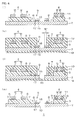
- FIG. 1 is a plan view of a suspension board with circuit produced by a producing method of a suspension board with circuit according to an embodiment of the present invention.
- FIGS. 2 to 4 are producing process views of the producing method of the suspension board with circuit shown in FIG. 1 , which are each taken along the line A-A of FIG. 1 .
- an insulating base layer 3 and an insulating cover layer 11, each described later, are omitted for clear illustration of relative positioning of a conductive pattern 4 to a metal supporting board 2.
- the conductive pattern 4 for connecting a magnetic head (not shown) of a hard disk drive and a read/write board (not shown) is formed integrally on the metal supporting board 2 on which the magnetic head is mounted.
- the conductive pattern 4 integrally includes magnetic-head-side connection terminal portions 5A for connecting to a terminal of the magnetic head as an electronic component, external connection terminal portions 5B for connecting to a terminal of the read/write board as an electronic component, and a plurality of wires 6 for connecting the magnetic-head-side connection terminal portions 5A and the external connection terminal portions 5B (which may be hereinafter collectively and simply referred to as "terminal portions 5").
- the metal supporting board 2 is formed in a flat belt-like shape extending in a longitudinal direction.
- the magnetic-head-side connection terminal portions 5A are provided at one longitudinal end portion (hereinafter referred to as a front end portion) of the metal supporting board 2.
- the external connection terminal portions 5B are provided at the other longitudinal end portion (hereinafter referred to as a rear end portion) of the metal supporting board 2.
- the front end portion of the suspension board with circuit 1 is also provided with a gimbal 22 for mounting the magnetic head and a reference hole 10.
- the gimbal 22 is formed at the portion where the magnetic head is mounted.
- the gimbal 22 is formed with cut-away portions 21 sandwiching the magnetic-head-side connection terminal portions 5A therebetween in the longitudinal direction.
- the reference hole 10 is used as a reference in positioning the magnetic head when the magnetic head is mounted.
- the reference hole 10 is formed at a widthwise midpoint and rearward of the gimbal 22 to have a generally circular shape when viewed in plan view, and extend through the metal supporting board 2 in the thickness direction thereof.
- the diameter of the reference hole 10 is in the range of, e.g., 300 to 1000 ⁇ m.
- the suspension board with circuit 1 includes the metal supporting board 2, the insulating base layer 3 as an insulating layer formed on the metal supporting board 2, the conductive pattern 4 formed on the insulating base layer 3, and the insulating cover layer 11 formed on the insulating base layer 3 so as to cover the conductive pattern 4.
- the insulating base layer 3 is formed on the surface of the metal supporting board 2 to correspond to the portion where the conductive pattern 4 is formed.
- the conductive pattern 4 is formed of a seed film 7 laminated on the surface of the metal supporting board 2, and a conductive layer 8 laminated on the surface (upper surface) of the seed film 7.
- the insulating cover layer 11 is formed so as to cover the wires 6, and expose the terminal portions 5 as well as a mark 9 described later.
- the mark 9 is provided on the front side of the suspension board with circuit 1.
- the mark 9 is disposed on the peripheral edge of the reference hole 10, and formed in a generally annular shape when viewed in plan view.
- the mark 9 is made of the seed film 7, and the conductive layer 8 formed on the top (upper surface) of the seed film 7, and formed with an opening 16 for forming the reference hole 10, which has a generally circular shape when viewed in plan view.
- the opening 16 is formed to be at the same position as that of the reference hole 10 when viewed in plan view.
- the inner end portion 15 of the conductive layer 8 of the mark 9 is removed by etching when the reference hole 10 is formed, which is described later.
- the conductive layer 8 of the mark 9 is formed so as to expose the portion of the seed film 7 from which the inner end portion 15 is removed, and surround the reference hole 10 in spaced apart relation when viewed in plan view.
- the metal supporting board 2 is prepared in the method.
- Examples of a metal material used to form the metal supporting board 2 include stainless steel, and a 42-alloy. Preferably, stainless steel is used.
- the thickness of the metal supporting board 2 is in the range of, e.g., 10 to 60 ⁇ m, or preferably 15 to 30 ⁇ m.
- the insulating base layer 3 is formed on the metal supporting board 2.
- Examples of an insulating material used to form the insulating base layer 3 include synthetic resins such as a polyimide resin, a polyamide imide resin, an acrylic resin, a polyether nitrile resin, a polyether sulfone resin, a polyethylene terephthalate resin, a polyethylene naphthalate resin, a polyvinyl chloride resin, and a fluorine resin.
- synthetic resins such as a polyimide resin, a polyamide imide resin, an acrylic resin, a polyether nitrile resin, a polyether sulfone resin, a polyethylene terephthalate resin, a polyethylene naphthalate resin, a polyvinyl chloride resin, and a fluorine resin.
- a photosensitive synthetic resin is used, or more preferably a photosensitive polyimide resin is used.
- a photosensitive polyimide resin e.g., a varnish (a photosensitive polyamic acid resin solution) of a photosensitive polyimide resin precursor is uniformly coated first on the surface of the metal supporting board 2, and dried by heating at a temperature of, e.g., 70 to 120 °C to form a base coating. Then, the base coating is exposed to light via a photomask not shown, developed, and then cured (imidized) by heating at a temperature of 300°C or more to form the insulating base layer 3 in the foregoing pattern.
- a photosensitive polyimide resin e.g., a varnish (a photosensitive polyamic acid resin solution) of a photosensitive polyimide resin precursor is uniformly coated first on the surface of the metal supporting board 2, and dried by heating at a temperature of, e.g., 70 to 120 °C to form a base coating. Then, the base coating is exposed to light via a photomask not shown, developed, and then cured (imidized) by heating
- the thickness of the insulating base layer 3 thus formed is in the range of, e.g., 1 to 30 ⁇ m, or preferably 2 to 20 ⁇ m.
- the conductive pattern 4 and the mark 9 are simultaneously formed by an additive method.
- the seed film 7 is formed first on the insulating base layer 3, and on the metal supporting board 2 exposed from the insulating base layer 3, as shown in FIG. 2(c) .
- Examples of a material used to form the seed film 7 include metal materials such as chromium, gold, silver, platinum, nickel, titanium, silicon, manganese, zirconium, an alloy thereof, and an oxide thereof. Preferably, chromium is used.
- the seed film 7 may also be formed of a plurality of layers.
- the seed film 7 is formed by, e.g., sputtering, electrolytic plating, or electroless plating.
- the seed film 7 is formed by sputtering.
- sputtering sputtering which sputters the metal mentioned above as a target is used.
- chromium sputtering is used, whereby a chromium thin film is laminated.
- the thickness of the seed film 7 thus formed is in the range of, e.g., 0.01 to 1 ⁇ m, or preferably 0.01 to 0.1 ⁇ m.
- a photoresist 12 is laminated on the seed film 7.
- a dry film resist e.g., is laminated on the surface of the seed film 7.
- the photoresist 12 is exposed to light via a photomask 13, and then developed, as shown in FIG. 3(f) , to form a plating resist 14 in a pattern reverse to the conductive pattern 4, and to the pattern of the mark 9.
- a pattern for forming the conductive pattern 4, and a pattern for forming the mark 9 are integrally formed in the single photomask 13.
- the photomask 13 includes light shield portions 13a which do not allow transmission of light therethrough, and light transmission portions 13b which allow transmission of light therethrough in the foregoing pattern.
- the photomask 13 is disposed to oppose the light shield portions 13a to the portions where the conductive pattern 4 and the mark 9 are formed, and oppose the light transmission portions 13b to the portions where the conductive pattern 4 and the mark 9 are not formed, and then the photoresist 12 is exposed to light.
- the unexposed portions opposed to the light shield portions 13a i.e., the portions where the conductive pattern 4 and the mark 9 are formed are removed by development.
- a dipping method, a spraying method, or the like is used for the development.
- the plating resist 14 is formed in the pattern reverse to the conductive pattern 4, and to the pattern of the mark 9 on the surface of the seed film 7.
- the photomask 13 is disposed by reversing the respective positions of the light shield portions 13a and the light transmission portions 13b, i.e., by opposing the light transmission portions 13b of the photomask 13 to the portions where the conductive pattern 4 and the mark 9 are formed, and then the photoresist 12 is exposed to light, and developed.
- the conductive layer 8 is laminated on the seed film 7 exposed from the plating resist 14.
- Examples of a conductive material used to form the conductive layer 8 include metals such as copper, nickel, gold, a solder, and an alloy thereof. Among them, copper is preferably used.
- the conductive layer 8 is laminated by, e.g., electrolytic plating, or preferably electrolytic copper plating.
- the thickness of the conductive layer 8 thus laminated is in the range of, e.g., 5 to 20 ⁇ m, or preferably 5 to 15 ⁇ m.
- the plating resist 14 is removed.
- the plating resist 14 is removed by, e.g., etching, stripping, or the like.
- the seed film 7 exposed from the conductive layer 8 is removed by, e.g., etching, stripping, or the like.
- the conductive pattern 4 and the mark 9, each made of the seed film 7 and the conductive pattern 8, can be simultaneously formed.
- the insulating cover layer 11 is formed in the foregoing pattern on the insulating base layer 3.
- the same insulating material as used to form the insulating base layer 3 mentioned above is used.
- a photosensitive polyimide resin e.g., a varnish (a photosensitive polyamic acid resin solution) of a photosensitive polyimide resin precursor is uniformly coated first on the surface of the insulating base layer 3 including the conductive pattern 4 and the mark 9, and dried by heating at a temperature of, e.g., 70 to 120°C to form a cover coating. Then, the cover coating is exposed to light via a photomask not shown, developed, and then cured (imidized) by heating at a temperature of 300°C or more to form the insulating cover layer 11 in the foregoing pattern.
- a photosensitive polyimide resin e.g., a varnish (a photosensitive polyamic acid resin solution) of a photosensitive polyimide resin precursor is uniformly coated first on the surface of the insulating base layer 3 including the conductive pattern 4 and the mark 9, and dried by heating at a temperature of, e.g., 70 to 120°C to form a cover coating. Then, the cover coating is exposed to light
- the thickness of the insulating cover layer 11 thus formed is in the range of, e.g., 2 to 10 ⁇ m, or preferably 3 to 6 ⁇ m.
- a second etching resist 19 is formed first to cover the conductive pattern 4, and partly expose the mark 9, as shown in FIG. 4(k) .
- the second etching resist 19 is formed to expose the inner end portion 15 of the conductive layer 8 having a generally annular shape when viewed in plan view in the mark 9.
- the width W1 of the inner end portion 15 of the conductive layer 8 exposed from the second etching resist 19 is in the range of, e.g., 20 to 60 ⁇ m.
- the second etching resist 19 is formed in the foregoing pattern by, e.g., laminating a dry film resist on the surface of the insulating base layer 3 including the conductive pattern 4 and the mark 9, on the surface of the insulating cover layer 11, and on the back surface of the metal supporting board 2 and then exposing the dry film to light, and developing it.
- the inner end portion 15 of the conductive layer 8 exposed from the second etching resist 19 is etched using the second etching resist 19 as an etching resist (mask), and the metal supporting board 2 exposed from the seed film 7 of the mark 9 is etched using the seed film 7 as an etching resist (mask).
- etching chemical etching using, e.g., an etchant such as ferric chloride aqueous solution dissolving copper and stainless steel is used.
- an etchant such as ferric chloride aqueous solution dissolving copper and stainless steel
- the second etching resist 19 is removed.
- the second etching resist 19 is removed by, e.g., etching, stripping, or the like.
- the conductive pattern 4 and the mark 9 are simultaneously formed in the method, the conductive pattern 4 and the mark 9 can be accurately positioned relatively to each other.
- the conductive pattern 4 and the mark 9 can be accurately positioned relatively to each other.
- the reference hole 10 can be reliably formed by a simple and convenient method.
- the reference hole 10 can be formed by a simple and easy method in which only the metal supporting board 2 is etched.
- the reference hole 10 and the opening 16 are each formed in the generally circular shape when viewed in plan view. However, it is also possible to form the reference hole 10 and the opening 16 each in an appropriate shape such as, e.g., a rectangular shape when viewed in plan view.
- the second etching resist 19 is used as the etching resist (mask) in the etching of the conductive layer 8.
- the insulating cover layer 11 is also possible to use, e.g., the insulating cover layer 11 as the etching resist (mask), as shown in FIG. 5(l) .
- the insulating cover layer 11 is formed so as to partly expose the mark 9. Specifically, the insulating cover layer 11 is formed in a pattern formed with a cover opening 28 for exposing the opening 16 of the mark 9. In short, the insulating cover layer 11 is formed to expose the surfaces (upper surface and inner side surface) of the inner end portion 15 of the mark 9, and cover the surfaces (upper surface and outer side surface) of an outer end portion 17 of the mark 9.
- the insulating cover layer 11 is formed in the foregoing pattern, as shown in fig. 5(j) .
- the second etching resist 19 is formed so as to cover the conductive pattern 4, cover an outer end portion 27 of the insulating cover layer 11, and expose an inner end portion 26 of the insulating cover layer 11.
- the end edge of the opening for exposing the cover opening 28 is disposed outside (longitudinally outward and widthwise outward) and spaced apart from the cover opening 28.
- the inner end portion 15 of the conductive layer 8 of the mark 9 exposed from the cover opening 28 is etched using the insulating cover layer 11 as an etching resist (mask).
- the metal supporting board 2 exposed from the seed film 7 is etched using the seed film 7 of the mark 9 as an etching resist.
- the same etching as mentioned above is used for the etching of the conductive layer 8 and the metal supporting board 2.
- the second etching resist 19 is removed in the same manner as described above.
- the conductive layer 8 of the mark 9 can be etched using the insulating cover layer 11 as the etching resist.
- the insulating base layer 3 is formed on the surface of the metal supporting board 2 to correspond to the portions where the conductive pattern 4 and the mark 9 are formed.
- the reference hole 10 is opened to extend through the metal supporting board 2 and the insulating base layer 3 in the thickness direction thereof.
- the metal supporting board 2 is prepared in the method.
- a metal material for forming the metal supporting board 2, and the thickness of the metal supporting board 2 are the same as mentioned above.
- the insulating base layer 3 is formed in the foregoing pattern on the metal supporting board 2.
- the same method as described above is used for the formation of the insulating base layer 3.
- the conductive pattern 4 and the mark 9 are simultaneously formed by an additive method.
- the seed film 7 is formed first on the insulating base layer 3, and on the metal supporting board 2 exposed from the insulating base layer, as shown in FIG. 6(c) .
- the seed film 7 is formed by the same method as described above.
- the photoresist 12 is laminated on the seed film 7.
- the photoresist 12 is laminated by the same method as described above.
- the photoresist 12 is exposed to light via the photomask 13, and then developed, as shown in FIG. 7(f) , to form the plating resist 14 in a pattern reverse to the conductive pattern 4, and to the pattern of the mask 9.
- the same method as described above is used for the exposure of the photoresist 12 to light and the development thereof.
- the conductive layer 8 is laminated on the seed film 7 exposed from the plating resist 14.
- the conductive layer 8 is laminated by the same method as described above.
- the plating resist 14 is removed by the same method as described above.
- the seed film 7 exposed from the conductive layer 8 is removed by the same method as described above.
- the conductive pattern 4 and the mark 9, each made of the seed film 7 and the conductive layer 8, can be formed simultaneously.
- the insulating cover layer 11 is formed in the foregoing pattern on the insulating base layer 3.
- the same method as described above is used for the formation of the insulating cover layer 11.
- the reference hole 10 is formed.
- the second etching resist 19 is formed first so as to cover the conductive pattern 4, and partly expose the mark 9 in the same manner as described above, as shown in FIG. 8(k) .
- the conductive layer 8 exposed from the second etching resist 19 is etched using the second etching resist 19 as an etching resist.
- the insulating base layer 3 exposed from the seed film 7 is etched using the seed film 7 as an etching resist (mask).
- etching resist For the etching of the insulating base layer 3, chemical etching using an alkaline aqueous solution or the like is used.
- the inner end portion 15 of the conductive layer 8 exposed from the second etching resist 19 is etched using the second etching resist 19 as an etching resist (mask), and the metal supporting board 2 exposed from the seed film 7 is etched using the seed film 7 as an etching resist (mask).
- the same etching as mentioned above is used for the etching of the conductive layer 8 and the metal supporting board 2.
- the second etching resist 19 is removed in the same manner as described above.
- the conductive pattern 4 and the mark 9 are both formed on the insulating base layer 3 in the method, more accurate relative positioning can be ensured.
- the second etching resist 19 is used as an etching resist (mask) in the etching of the conductive layer 8.
- the insulating cover layer 11 is formed to cover the mark 9 in the producing of the suspension board with circuit 1.
- the insulating cover layer 11 is formed to be filled in the opening 16 of the mark 9, and cover the surfaces (upper surface and both side surfaces) of the mark 9.
- the insulating cover layer 11 is formed in the foregoing pattern, as shown in FIG. 9(j) .
- the second etching resist 19 is formed to cover the conductive pattern 4, cover the outer end portions 27 of the insulating cover layer 11 formed on the surface (upper surface) of the mark 9, and expose a middle portion 29.
- the middle portion 29 of the insulating cover layer 11 exposed from the second etching resist 19 is etched using the second etching resist 19 as an etching resist.
- the insulating base layer 3 exposed from the mark 9 is etched using the mark 9 as an etching resist.
- the same etching as used for the etching of the insulating base layer 3 is used.
- the metal supporting board 2 exposed from the seed film 7 is etched using the seed film 7 as an etching resist.
- the same method as described above is used for the etching of the metal supporting board 2.
- the second etching resist 19 is removed in the same manner as described above.
- the conductive layer 8 can be etched using both of the second etching resist 19 and the insulating cover layer 11 as the etching resist.
- the conductive pattern 4 and the mark 9 are formed by the additive method. However, it is also possible to form the conductive pattern 4 and the mark 9 by, e.g., a subtractive method, as shown in FIGS. 10 and 11 .
- a four-layer base material 24 laminated with the metal supporting board 2, the insulating base layer 3, the seed film 7, and the conductive layer 8 in this order is prepared first, as shown in FIG. 10(a) .
- the insulating base layer 3 is laminated on the metal supporting board 2
- the seed film 7 is laminated on the insulating base layer 3
- the conductive layer 8 is formed on the seed film 7.
- a metal material for forming the metal supporting board 2 an insulating material for forming the insulating base layer 3, a material for forming the seed film 7, and a conductive material for forming the conductive layer 8 are the same as mentioned above.
- the respective thicknesses of the metal supporting board 2, the insulating base layer 3, the seed film 7, and the conductive layer 8 are also the same as mentioned above.
- the photoresist 12 is laminated on the conductive layer 8 (conductive layer 8 laminated on the insulating base layer 3 via the seed film 7).
- the photoresist 12 is laminated by the same method as described above.
- the photoresist 12 is exposed to light via the photomask 13, and then developed, as shown in FIG. 10(d) , to form a first etching resist 18 in the same pattern as the conductive pattern 4, and as the pattern of the mark 9.
- the light transmission portions 13b are opposed to the portions where the conductive pattern 4 and the mark 9 are formed, and then the photoresist 12 is exposed to light, and developed.
- the first etching resist 18 is formed in the same pattern as the conductive pattern 4, and as the pattern of the mark 9 on the surface of the conductive layer 8.
- the conductive layer 8 and the seed film 7, each exposed from the first etching resist 18, are etched.
- chemical etching using, e.g., an etchant is used for the etching of the conductive layer 8 and the seed film 7.
- the conductive pattern 4 and the mark 9, each made of the conductive layer 8 and the seed film 7, are formed by the subtractive method.
- the first etching resist 18 is removed.
- the first etching resist 18 is removed by, e.g., etching, stripping, or the like.
- the insulating cover layer 11 is formed in the foregoing pattern on the insulating base layer 3.
- the same method as described above is used for the formation of the insulating cover layer 11.
- the reference hole 10 is formed.
- the same method as described in FIGS. 8(k) to 8(m) is used.
- the conductive pattern 4 and the mark 9 are both formed on the insulating base layer 3 in the method, more accurate relative positioning can be ensured.
- the conductive pattern 4 and the mark 9 are formed by the subtractive method using the four-layer base material 24, the number of steps for forming the conductive layer 8 and the seed film 7 can be reduced.
- the four-layer base material 24 is prepared, preliminarily laminated with the metal supporting board 2, the insulating base layer 3, the seed film 7, and the conductive layer 8.
- the metal supporting board 2 it is also possible to, e.g., successively laminate the individual layers and the film each mentioned above, though not shown.
- the metal supporting board 2 it is also possible to prepare the metal supporting board 2 first, laminate the insulating base layer 3 on the metal supporting board 2, laminate the seed film 7 on the insulating base layer 3, and then laminate the conductive layer 8 thereon.
- metal plating layers 23 are formed on the surfaces of the terminal portions 5. Specifically, the metal plating layer 23 is formed on the side surfaces and top surfaces of the terminal portions 5.
- the metal plating layer 23 is also formed on the mark 9. Specifically, the metal plating layer 23 is formed on the surfaces (top surface and side surfaces) of the mark 9.
- the metal supporting board 2 is prepared in the method.
- a metal material for forming the metal supporting board 2, and the thickness of the metal supporting board 2 are the same as mentioned above.
- the insulating base layer 3 is formed on the surface of the metal supporting board 2.
- the same method as described above is used for the formation of the insulating base layer 3.
- the conductive pattern 4 and the mark 9 are simultaneously formed by an additive method.
- the insulating cover layer 11 is formed in the foregoing pattern on the insulating base layer 3.
- the same method as described above is used for the formation of the insulating cover layer 11.
- the metal plating layers 23 are formed on the respective surfaces of the terminal portions 5 and the mark 9.
- Examples of a metal used to form the metal plating layers 23 include a metal which is not corroded by etching described later, such as, e.g., chromium, gold, silver, platinum, nickel, titanium, manganese, zirconium, or tin. In terms of corrosion resistance by an etchant, gold is preferably used.
- the metal plating layer 23 is formed by, e.g., electroless plating or the like, or preferably electroless gold plating.
- the thickness of the metal plating layer 23 thus formed is in the range of, e.g., 0.01 to 1 ⁇ m, or preferably 0.01 to 0.1 ⁇ m.
- the reference hole 10 is formed.
- the second etching resist 19 is formed first so as to cover the insulating cover layer 11 and the metal plating layers 23 of the terminal portions 5, and partly expose the metal plating layer 23 on the surface of the mark 9, as shown in FIG. 14(l) .
- the second etching resist 19 is formed to expose the inner end portion 15 of the conductive layer 8 having the generally annular shape when viewed in plan view at the surface of the mark 9.
- the insulating base layer 3 exposed from the metal plating layer 23 formed on the surface of the mark 9 is etched using the metal plating layer 23 formed on the surface of the mark 9 as an etching resist (mask).
- the metal supporting board 2 exposed from the metal plating layer 23 formed on the surface of the mark 9 is etched using the metal plating layer 23 formed on the surface of the mark 9 as an etching resist (mask).
- the second etching resist 19 is removed by the same method as described above.
- the reference hole 10 can be formed.
- the insulating base layer 3 and the metal supporting board 2, both exposed from the metal plating layers 23, are etched using the metal plating layers 23 as the etching resist. Therefore, it is possible to reliably form the reference hole 10 by a simple and convenient method.
- the insulating cover layer 11 is formed, and then metal plating layers 23 are formed.
- the formation order of the insulating cover layer 11 and the metal plating layers 23 is not limited thereto.
- the metal plating layers 23 are formed also on the surfaces of the wires 6.
- the conductive pattern 4 and the mark 9 are formed by the additive method. However, it is also possible to form the conductive pattern 4 and the mark 9 by, e.g., a subtractive method, as shown in FIGS. 15(a) to 15(f) .
- the conductive pattern 4 and the mark 9 are each formed only of the conductive layer 8.
- a three-layer base material 25 laminated with the metal supporting board 2, the insulating base layer 3, and the conductive layer 8 are preliminarily prepared first.
- the insulating base layer 3 is laminated on the metal supporting board 2, and the conductive layer 8 is formed on the insulating base layer 3.
- the photoresist 12 is laminated directly on the conductive layer 8, as shown in FIG. 15(b) .
- the photoresist 12 is laminated by the same method as described above.
- the photoresist 12 is exposed to light via the photomask 13, and then developed, as shown in FIG. 15(d) , to form the first etching resist 18 in the same pattern as the conductive pattern 4, and as the pattern of the mark 9.
- the same method as described above is used for the exposure to light and the development via the photomask 13, the same method as described above is used.
- the conductive layer 8 exposed from the first etching resist 18 is etched.
- the same method as described above is used for the etching of the conductive layer 8.
- the conductive pattern 4 and the mark 9, each made of the conductive layer 8, are formed by the subtractive method.
- the first etching resist 18 is removed.
- the same method as mentioned above is used for the removal of the first etching resist 18.
- the insulating cover layer 11 is formed in the foregoing pattern on the insulating base layer 3.
- the same method as described above is used for the formation of the insulating cover layer 11.
- the metal plating layers 23 are formed on the respective surfaces of the terminal portions 5 and the mark 9.
- the same method as mentioned above is used for the formation of the metal plating layers 23.
- the reference hole 10 is formed.
- the same method as described in FIGS. 14(l) and 14(m) is used.
- the conductive pattern 4 and the mark 9 are formed by the subtractive method using the three-layer base material 25 in the method, the number of steps for forming the conductive layer 8 can be reduced.
- the subtractive method used in the method does not require the formation of the seed film 7. Accordingly, it is also possible to reduce the number of process steps for forming the seed film 7.
- the three-layer base material 25 is prepared, preliminarily laminated with the metal supporting board 2, the insulating base layer 3, and the conductive layer 8 in this order, as shown in FIG. 15(a) .
- a two-layer base material made of the insulating base layer 3, and the conductive layer 8 laminated on the insulating base layer 3, and then may be prepared the metal supporting board 2 may be bonded to the back surface (lower surface of the insulating base layer 3) of the two-layer base material.
- the three-layer base material 25 in which the seed film is not laminated is used.
- the four-layer base material 24 see FIG. 10(a) ) including the seed film 7.
Landscapes
- Engineering & Computer Science (AREA)
- Microelectronics & Electronic Packaging (AREA)
- Manufacturing & Machinery (AREA)
- Adjustment Of The Magnetic Head Position Track Following On Tapes (AREA)
- Supporting Of Heads In Record-Carrier Devices (AREA)
- Structure Of Printed Boards (AREA)
Abstract
Description
- The present application claims the benefit of
U.S. Provisional Application No. 60/935,054 filed on July 24, 2007 2007-180204 filed on July 9, 2007 2008-111653 filed on April 22, 2008 - The present invention relates to a producing method of a suspension board with circuit and, more particularly, to a producing method of a suspension board with circuit on which an electronic component is mounted.
- A suspension board with circuit is used in a hard disk drive. In the suspension board with circuit, a wired circuit pattern including terminal portions for connecting to a magnetic head is formed integrally on a suspension board for supporting the magnetic head. Specifically, the suspension board with circuit includes the suspension board made of stainless steel, an insulating base layer made of polyimide and formed on the suspension board, and the wired circuit pattern made of copper and formed on the insulating base layer.
- On such a suspension board with circuit, a magnetic head is mounted using tooling holes opened in a metal supporting board as a reference, and a terminal of the magnetic head is connected to the terminal portions (see, e.g., Japanese Unexamined Patent No.
2007-109725 - In the suspension board with circuit, an positioning mark is formed simultaneously with the formation of an insulating base layer. Using the positioning mark as a reference, a photomask for forming a wired circuit pattern is positioned, and a photomask for forming the tooling holes is further positioned.
- That is, in the method described above, the common positioning mark is used as the reference to first position the photomask for forming the wired circuit pattern during the formation of the wired circuit pattern, and then position the photomask for forming the tooling holes during the formation of the tooling holes.
- However, in the method described above, the photomask for forming the wired circuit pattern, and the photomask for forming the tooling holes are used individually in different process steps.
- As a result, it is possible to position the photomask for forming the wired circuit pattern or the photomask for forming the tooling holes with respect to the positioning mark. However, relative positioning of the formed wired circuit pattern and the formed tooling holes includes both of the tolerance of the photomask for forming the wired circuit pattern with respect to the positioning mark and the tolerance of the photomask for forming the tooling holes with respect to the positioning mark. Accordingly, it is difficult to improve accuracy.
- On the other hand, to mount the magnetic head using the tooling holes as a reference, and connect the terminal of the magnetic head and the terminal portions of the wired circuit pattern, it is necessary to effect accurate relative positioning of the tooling holes and the wired circuit pattern.
- It is therefore an object of the present invention to provide a producing method of a suspension board with circuit which allows accurate mounting of an electronic component, and accurate connection of a terminal of the electronic component and terminal portions of a conductive pattern.
- A producing method of a suspension board with circuit according to the present invention includes simultaneously forming a conductive pattern formed on an insulating layer formed on a metal supporting board and having a terminal portion for connecting to an electronic component, and a mark formed on the metal supporting board, or on the insulating layer and having an opening for forming a reference hole for mounting the electronic component, and forming the reference hole by etching the metal supporting board disposed in the opening of the mark, or the insulating layer and the metal supporting board each disposed in the opening of the mark.
- In the method, the conductive pattern and the mark are simultaneously formed. This allows accurate relative positioning of the conductive pattern and the mark.
- Since the reference hole is formed based on the opening of the mark, it is possible to reliably connect a terminal of the electronic component which is mounted using the reference mark as the reference, and the terminal portion which is accurately positioned relatively to the mark.
- As a result, a suspension board with circuit excellent in connection reliability can be obtained.
- In the producing method of the suspension board with circuit according to the present invention, it is preferable that, in the step of simultaneously forming the conductive pattern and the mark, the conductive pattern and the mark are each formed of a conductive layer, and of a seed film formed on a lower surface of the conductive layer and, in the step of forming the reference hole, the reference hole is formed by etching the metal supporting board exposed from the seed film of the mark, or the insulating layer and the metal supporting board each exposed from the seed film of the mark using the seed film as an etching resist.
- In the method, the metal supporting board exposed from the seed film of the mark is etched, or the insulating layer and the metal supporting board each exposed from the seed film of the mark are etched using the seed film as the etching resist. This allows reliable formation of the reference hole by a simple and convenient method.
- In the producing method of the suspension board with circuit according to the present invention, it is preferable that the step of simultaneously forming the conductive pattern and the mark includes forming the seed film on the insulating layer, and on the metal supporting board exposed from the insulating layer, laminating a photoresist on the seed film, exposing the photoresist to light via a photomask, and then developing the photoresist to form a plating resist in a pattern reverse to the conductive pattern, and to a pattern of the mark, laminating the conductive layer on the seed film exposed from the plating resist, removing the plating resist, and removing the seed film exposed from the conductive layer to form the conductive pattern and the mark, and the step of forming the reference hole includes forming a second etching resist so as to cover the conductive pattern, and partly expose the mark, etching the conductive layer of the partly exposed mark using the second etching resist as an etching resist, and etching the metal supporting board exposed from the seed film of the mark using the seed film as an etching resist to form the reference hole.
- In the method, by accurately forming the photomask, the conductive pattern and the mark can be more accurately positioned relatively to each other. In addition, the reference hole can be formed by a simple and convenient method in which only the metal supporting board is etched.
- In the producing method of the suspension board with circuit according to the present invention, it is preferable that the step of simultaneously forming the conductive pattern and the mark includes forming the seed film on the insulating layer, laminating a photoresist on the seed film, exposing the photoresist to light via a photomask, and then developing the photoresist to form a plating resist in a pattern reverse to the conductive pattern, and to a pattern of the mark, laminating the conductive layer on the seed film exposed from the plating resist, removing the plating resist, and removing the seed film exposed from the conductive layer to form the conductive pattern and the mark, and the step of forming the reference hole includes forming a second etching resist so as to cover the conductive pattern, and partly expose the mark, etching the conductive layer of the partly exposed mark using the second etching resist as an etching resist, and etching the insulating layer and the metal supporting board each exposed from the seed film of the mark using the seed film as an etching resist to form the reference hole.
- In the method, by accurately forming the photomask, the conductive pattern and the mark can be more accurately positioned relatively to each other. Since the conductive pattern and the mark are both formed in the insulating layer, more accurate relative positioning can be ensured.
- In the producing method of the suspension board with circuit according to the present invention, it is preferable that the step of simultaneously forming the conductive pattern and the mark includes laminating a photoresist on the conductive layer laminated on the insulating layer via the seed film, exposing the photomask to light via a photomask, and then developing the photoresist to form a first etching resist in the same pattern as the conductive pattern, and as a pattern of the mark, etching the conductive layer and the seed film each exposed from the first etching resist to form the conductive pattern and the mark, and removing the first etching resist, and the step of forming the reference hole includes forming a second etching resist so as to cover the conductive, and partly expose the mark, etching the conductive layer of the partly exposed mark using the second etching resist as an etching resist, and etching the insulating layer and the metal supporting board each exposed from the seed film of the mark using the seed film as an etching resist to form the reference hole.
- In the method, by accurately forming the photomask, the conductive pattern and the mark can be more accurately positioned relatively to each other. In addition, the number of process steps can be reduced.
- In the producing method of the suspension board with circuit according to the present invention, it is preferable that, in the step of simultaneously forming the conductive pattern and the mark, the conductive pattern and the mark are each formed of at least a conductive layer and, in the step of forming the reference hole, the reference hole is formed by forming metal plating layers on a surface of the conductive pattern, and on a surface of the mark, and then etching the insulating layer and the metal supporting board each exposed from the metal plating layer on the surface of the mark using the metal plating layer formed on the surface of the mark as an etching resist.
- In the method, since the etching is performed using the metal plating layer as the etching resist, the reference hole can be formed reliably by a simple and convenient method.
- In the producing method of the suspension board with circuit according to the present invention, it is preferable that the step of simultaneously forming the conductive pattern and the mark includes forming the seed film on the insulating layer, laminating a photoresist on the seed film, exposing the photoresist to light via a photomask, and then developing the photoresist to form a plating resist in a pattern reverse to the conductive pattern, and to a pattern of the mark, laminating the conductive layer on the seed film exposed from the plating resist, removing the plating resist, and removing the seed film exposed from the conductive layer to form the conductive pattern and the mark, and the step of forming the reference hole includes forming a second etching resist so as to cover the metal plating layer on the surface of the conductive pattern, and partly expose the metal plating layer on the surface of the mark.
- In the method, by accurately forming the photomask, the conductive pattern and the mark can be more accurately positioned relatively to each other.
- In the producing method of the suspension board with circuit according to the present invention, it is preferable that the step of simultaneously forming the conductive pattern and the mark includes laminating a photoresist on the conductive layer laminated on the insulating layer, exposing the photoresist to light via a photomask, and then developing the photoresist to form a first etching resist in the same pattern as the conductive pattern, and as a pattern of the mark, etching the conductive layer exposed from the first etching resist to form the conductive pattern and the mark, and removing the first etching resist, and the step of forming the reference hole includes forming a second etching resist so as to cover the metal plating layer on the surface of the conductive pattern, and partly expose the metal plating layer on the surface of the mark.
- In the method, by accurately forming the photomask, the conductive pattern and the mark can be more accurately positioned relatively to each other. In addition, the number of process steps can be reduced.
- In the producing method of the suspension board with circuit according to the present invention, it is preferable that, in the step of simultaneously forming the conductive pattern and the mark, the photoresist is exposed to light via the single photomask.
- In the method, the photoresist is formed through one-time exposure to light via the single photomask to allow accurate relative positioning of the conductive pattern and the mark.
-
-
FIG. 1 is a plan view of a suspension board with circuit produced by a producing method of a suspension board with circuit according to an embodiment of the present invention; -
FIG. 2 is a producing process view of the producing method of the suspension board with circuit shown inFIG. 1 , which is taken along the line A-A ofFIG. 1 ,- (a) showing the step of preparing a metal supporting board,
- (b) showing the step of forming an insulating base layer on the metal supporting board,
- (c) showing the step of forming a seed film on the insulating base layer, and on the metal supporting board exposed from the insulating base layer,
- (d) showing the step of laminating a photoresist on the seed film, and
- (e) showing the step of exposing the photoresist to light via a photomask;
-
FIG. 3 is a producing process view of the producing method of the suspension board with circuit shown inFIG. 1 , subsequently toFIG. 2 , which is taken along the line A-A ofFIG. 1 ,- (f) showing the step of developing the photoresist to form a plating resist in a pattern reverse to a conductive pattern, and to the pattern of a mark,
- (g) showing the step of laminating a conductive layer on the seed film exposed from the plating resist,
- (h) showing the step of removing the plating resist, and
- (i) showing the step of removing the seed film exposed from the conductive layer;
-
FIG. 4 is a producing process view of the producing method of the suspension board with circuit shown inFIG. 1 , subsequently toFIG. 3 , which is taken along the line A-A ofFIG. 1 ,- (j) showing the step of forming an insulating cover layer on the insulating base layer,
- (k) showing the step of forming a second etching resist so as to cover the conductive pattern, and partly expose the mark,
- (l) showing the step of etching the metal supporting board exposed from the seed film, and
- (m) showing the step of removing the second etching resist;
-
FIG. 5 is a producing process view of the producing method of the suspension board with circuit according to another embodiment of the present invention, which corresponds toFIGS. 4(j) to 4(m) ,- (j) showing the step of forming the insulating cover layer on the insulating base layer so as to partly expose the mark,
- (k) showing the step of forming the second etching resist so as to cover the conductive pattern, and expose the inner end portion of the insulating cover layer formed on the upper surface of the mark,
- (l) showing the step of etching the conductive layer of the mark exposed from the insulating cover layer, and exposing the metal supporting board exposed from the seed film, and
- (m) showing the step of removing the second etching resist;
-
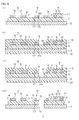
FIG. 6 is a producing process view of the producing method of the suspension board with circuit according to still another embodiment of the present invention, which is taken along the line A-A ofFIG. 1 ,- (a) showing the step of preparing the metal supporting board,
- (b) showing the step of forming the insulating base layer on the metal supporting board,
- (c) showing the step of forming the seed film on the insulating base layer, and on the metal supporting board exposed from the insulating base layer,
- (d) showing the step of laminating the photoresist on the seed film, and
- (e) showing the step of exposing the photoresist to light via the photomask;
-
FIG. 7 is a producing process view of the producing method of the suspension board with circuit according to the still another embodiment of the present invention, subsequently toFIG. 6 , which is taken along the line A-A ofFIG. 1 ,- (f) showing the step of developing the photoresist to form the plating resist in the pattern reverse to the conductive pattern, and to the pattern of the mark,
- (g) showing the step of laminating the conductive layer on the seed film exposed from the plating resist,
- (h) showing the step of removing the plating resist, and
- (i) showing the step of removing the seed film exposed from the conductive layer;
-
FIG. 8 is a producing process view of the producing method of the suspension board with circuit according to the still another embodiment of the present invention, subsequently toFIG. 7 , which is taken along the line A-A ofFIG. 1 ,- (j) showing the step of forming the insulating cover layer on the insulating base layer,
- (k) showing the step of forming the second etching resist so as to cover the conductive pattern, and partly expose the mark,
- (l) showing the step of etching the conductive layer exposed from a cover opening of the insulating cover layer, and the insulating base layer exposed from the seed film, and
- (m) showing the step of etching the metal supporting board exposed from the seed film, and removing the second etching resist;
-
FIG. 9 is a producing process view of the producing method of the suspension board with circuit according to yet another embodiment of the present invention, which corresponds toFIGS. 8(j) to 8(m) ,- (j) showing the step of forming the insulating cover layer on the insulating base layer so as to cover the mark,
- (k) showing the step of forming the second etching resist so as to cover the conductive pattern, and expose the inner end portion of the insulating cover layer formed on the upper surface of the mark,
- (l) showing the step of etching the insulating cover layer exposed from the second etching resist, and etching the insulating base layer exposed from the mark,
- (m) showing the step of etching the conductive layer exposed from the cover opening of the insulating cover layer, and etching the metal supporting board exposed from the seed film, and
- (n) showing the step of removing the second etching resist;
-
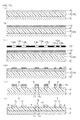
FIG. 10 is a producing process view of the producing method of the suspension board with circuit according to still another embodiment of the present invention, which is taken along the line A-A ofFIG. 1 ,- (a) showing the step of preparing a four-layer base material laminated with the metal supporting board, the insulating base layer, the seed film, and the conductive layer in this order,
- (b) showing the step of laminating the photoresist on the conductive layer,
- (c) showing the step of exposing the photoresist to light via the photomask,
- (d) showing the step of developing the photoresist to form a first etching resist in the same pattern as the conductive pattern, and as the pattern of the mark, and
- (e) showing the step of etching the conductive layer and the seed film each exposed from the first etching resist;
-
FIG. 11 is a producing process view of the producing method of the suspension board with circuit according to the still another embodiment of the present invention, subsequently toFIG. 10 , which is taken along the line A-A ofFIG. 1 ,- (f) showing the step of removing the first etching resist,
- (g) showing the step of forming the insulating cover layer on the insulating base layer,
- (h) showing the step of forming the second etching resist so as to cover the conductive pattern, and partly expose the mark,
- (i) showing the step of etching the insulating base layer exposed from the seed film, and
- (j) showing the step of etching the metal supporting board exposed from the seed film, and removing the second etching resist;
-
FIG. 12 is a producing process view of the producing method of the suspension board with circuit according to yet another embodiment of the present invention, which is taken along the line A-A ofFIG. 1 ,- (a) showing the step of preparing the metal supporting board,
- (b) showing the step of forming the insulating base layer on the metal supporting board,
- (c) showing the step of forming the seed film on the insulating base layer, and on the metal supporting board exposed from the insulating base layer,
- (d) showing the step of laminating the photoresist on the seed film, and
- (e) showing the step of exposing the photoresist to light via the photomask;
-
FIG. 13 is a producing process view of the producing method of the suspension board with circuit according to the yet another embodiment of the present invention, subsequently toFIG. 12 , which is taken along the line A-A ofFIG. 1 ,- (f) showing the step of developing the photoresist to form the plating resist in the pattern reverse to the conductive pattern, and to the pattern of the mark,
- (g) showing the step of laminating the conductive layer on the seed film exposed from the plating resist,
- (h) showing the step of removing the plating resist, and
- (i) showing the step of removing the seed film exposed from the conductive layer;
-
FIG. 14 is a producing process view of the producing method of the suspension board with circuit according to the yet another embodiment of the present invention, subsequently toFIG. 13 , which is taken along the line A-A ofFIG. 1 ,- (j) showing the step of forming the insulating cover layer on the insulating base layer,
- (k) showing the step of forming metal plating layers on the surfaces of terminal portions, and on the surface of the mark,
- (l) showing the step of forming the second etching resist so as to partly expose the metal plating layer on the surface of the mark, and subsequently etching the insulating base layer exposed from the metal plating layer formed on the surface of the mark using the metal plating layer as an etching resist, and
- (m) showing the step of etching the metal supporting board exposed from the metal plating layer, and then removing the second etching resist;
-
FIG. 15 is a producing process view of the producing method of the suspension board with circuit according to still another embodiment of the present invention, which is taken along the line A-A ofFIG. 1 ,- (a) showing the step of preparing a three-layer base material laminated with the metal supporting board, the insulating base layer, and the conductive layer in this order,
- (b) showing the step of laminating the photoresist on the conductive layer,
- (c) showing the step of exposing the photoresist to light via the photomask,
- (d) showing the step of developing the photoresist to form the first etching resist in the same pattern as the conductive pattern, and as the pattern of the mark,
- (e) showing the step of etching the conductive layer exposed from the first etching resist, and
- (f) showing the step of removing the first etching resist;
-
FIG. 16 is a producing process view of the producing method of the suspension board with circuit according to the still another embodiment of the present invention, subsequently toFIG. 15 , which is taken along the line A-A ofFIG. 1 ,- (g) showing the step of forming the insulating cover layer on the insulating base layer,
- (h) showing the step of forming the metal plating layers on the surfaces of the terminal portions, and on the surface of the mark,
- (i) showing the step of forming the second etching resist so as to partly expose the metal plating layer on the surface of the mark, and subsequently etching the insulating base layer exposed from the metal plating layer, and
- (j) showing the step of etching the metal supporting board exposed from the metal plating layer, and then removing the second etching resist.
-
FIG. 1 is a plan view of a suspension board with circuit produced by a producing method of a suspension board with circuit according to an embodiment of the present invention.FIGS. 2 to 4 are producing process views of the producing method of the suspension board with circuit shown inFIG. 1 , which are each taken along the line A-A ofFIG. 1 . InFIG. 1 , an insulatingbase layer 3 and an insulatingcover layer 11, each described later, are omitted for clear illustration of relative positioning of aconductive pattern 4 to ametal supporting board 2. - In
FIG. 1 , in a suspension board withcircuit 1, theconductive pattern 4 for connecting a magnetic head (not shown) of a hard disk drive and a read/write board (not shown) is formed integrally on themetal supporting board 2 on which the magnetic head is mounted. - The
conductive pattern 4 integrally includes magnetic-head-side connection terminal portions 5A for connecting to a terminal of the magnetic head as an electronic component, externalconnection terminal portions 5B for connecting to a terminal of the read/write board as an electronic component, and a plurality ofwires 6 for connecting the magnetic-head-side connection terminal portions 5A and the externalconnection terminal portions 5B (which may be hereinafter collectively and simply referred to as "terminal portions 5"). - The
metal supporting board 2 is formed in a flat belt-like shape extending in a longitudinal direction. The magnetic-head-side connection terminal portions 5A are provided at one longitudinal end portion (hereinafter referred to as a front end portion) of themetal supporting board 2. The externalconnection terminal portions 5B are provided at the other longitudinal end portion (hereinafter referred to as a rear end portion) of themetal supporting board 2. - The front end portion of the suspension board with
circuit 1 is also provided with agimbal 22 for mounting the magnetic head and areference hole 10. - The
gimbal 22 is formed at the portion where the magnetic head is mounted. Thegimbal 22 is formed with cut-awayportions 21 sandwiching the magnetic-head-side connection terminal portions 5A therebetween in the longitudinal direction. - The
reference hole 10 is used as a reference in positioning the magnetic head when the magnetic head is mounted. Thereference hole 10 is formed at a widthwise midpoint and rearward of thegimbal 22 to have a generally circular shape when viewed in plan view, and extend through themetal supporting board 2 in the thickness direction thereof. The diameter of thereference hole 10 is in the range of, e.g., 300 to 1000 µm. - As shown in
FIG. 4(m) , the suspension board withcircuit 1 includes themetal supporting board 2, the insulatingbase layer 3 as an insulating layer formed on themetal supporting board 2, theconductive pattern 4 formed on the insulatingbase layer 3, and the insulatingcover layer 11 formed on the insulatingbase layer 3 so as to cover theconductive pattern 4. - The insulating
base layer 3 is formed on the surface of themetal supporting board 2 to correspond to the portion where theconductive pattern 4 is formed. - The
conductive pattern 4 is formed of aseed film 7 laminated on the surface of themetal supporting board 2, and aconductive layer 8 laminated on the surface (upper surface) of theseed film 7. - The insulating
cover layer 11 is formed so as to cover thewires 6, and expose theterminal portions 5 as well as amark 9 described later. - As shown in
FIG. 1 , themark 9 is provided on the front side of the suspension board withcircuit 1. - As shown in
FIGS. 1 and4(m) , themark 9 is disposed on the peripheral edge of thereference hole 10, and formed in a generally annular shape when viewed in plan view. Themark 9 is made of theseed film 7, and theconductive layer 8 formed on the top (upper surface) of theseed film 7, and formed with anopening 16 for forming thereference hole 10, which has a generally circular shape when viewed in plan view. - The
opening 16 is formed to be at the same position as that of thereference hole 10 when viewed in plan view. - The
inner end portion 15 of theconductive layer 8 of themark 9 is removed by etching when thereference hole 10 is formed, which is described later. As a result, theconductive layer 8 of themark 9 is formed so as to expose the portion of theseed film 7 from which theinner end portion 15 is removed, and surround thereference hole 10 in spaced apart relation when viewed in plan view. - Next, a description is given to a producing method of the suspension board with
circuit 1 with reference toFIGS. 2 to 4 . - First, as shown in
FIG. 2(a) , themetal supporting board 2 is prepared in the method. - Examples of a metal material used to form the
metal supporting board 2 include stainless steel, and a 42-alloy. Preferably, stainless steel is used. The thickness of themetal supporting board 2 is in the range of, e.g., 10 to 60 µm, or preferably 15 to 30 µm. - Next, as shown in
FIG. 2(b) , the insulatingbase layer 3 is formed on themetal supporting board 2. - Examples of an insulating material used to form the insulating
base layer 3 include synthetic resins such as a polyimide resin, a polyamide imide resin, an acrylic resin, a polyether nitrile resin, a polyether sulfone resin, a polyethylene terephthalate resin, a polyethylene naphthalate resin, a polyvinyl chloride resin, and a fluorine resin. Preferably, a photosensitive synthetic resin is used, or more preferably a photosensitive polyimide resin is used. - To form the insulating
base layer 3 using, e.g., a photosensitive polyimide resin, e.g., a varnish (a photosensitive polyamic acid resin solution) of a photosensitive polyimide resin precursor is uniformly coated first on the surface of themetal supporting board 2, and dried by heating at a temperature of, e.g., 70 to 120 °C to form a base coating. Then, the base coating is exposed to light via a photomask not shown, developed, and then cured (imidized) by heating at a temperature of 300°C or more to form the insulatingbase layer 3 in the foregoing pattern. - The thickness of the insulating
base layer 3 thus formed is in the range of, e.g., 1 to 30 µm, or preferably 2 to 20 µm. - Then, as shown in
FIGS. 2(c) to 3(i) , theconductive pattern 4 and themark 9 are simultaneously formed by an additive method. - When the
conductive pattern 4 and themark 9 are simultaneously formed by the additive method, theseed film 7 is formed first on the insulatingbase layer 3, and on themetal supporting board 2 exposed from the insulatingbase layer 3, as shown inFIG. 2(c) . - Examples of a material used to form the
seed film 7 include metal materials such as chromium, gold, silver, platinum, nickel, titanium, silicon, manganese, zirconium, an alloy thereof, and an oxide thereof. Preferably, chromium is used. Theseed film 7 may also be formed of a plurality of layers. - The
seed film 7 is formed by, e.g., sputtering, electrolytic plating, or electroless plating. Preferably, theseed film 7 is formed by sputtering. - For the sputtering, sputtering which sputters the metal mentioned above as a target is used. Preferably, chromium sputtering is used, whereby a chromium thin film is laminated.
- The thickness of the
seed film 7 thus formed is in the range of, e.g., 0.01 to 1 µm, or preferably 0.01 to 0.1 µm. - Next, as shown in
FIG. 2(d) , aphotoresist 12 is laminated on theseed film 7. - As the photoresist, a dry film resist, e.g., is laminated on the surface of the
seed film 7. - Then, as shown in
FIG. 2(e) , thephotoresist 12 is exposed to light via aphotomask 13, and then developed, as shown inFIG. 3(f) , to form a plating resist 14 in a pattern reverse to theconductive pattern 4, and to the pattern of themark 9. - As shown in
FIG. 2(e) , a pattern for forming theconductive pattern 4, and a pattern for forming themark 9 are integrally formed in thesingle photomask 13. Specifically, thephotomask 13 includeslight shield portions 13a which do not allow transmission of light therethrough, andlight transmission portions 13b which allow transmission of light therethrough in the foregoing pattern. In the case of performing patterning with a negative image, thephotomask 13 is disposed to oppose thelight shield portions 13a to the portions where theconductive pattern 4 and themark 9 are formed, and oppose thelight transmission portions 13b to the portions where theconductive pattern 4 and themark 9 are not formed, and then thephotoresist 12 is exposed to light. - Thereafter, as shown in
FIG. 3(f) , the unexposed portions opposed to thelight shield portions 13a, i.e., the portions where theconductive pattern 4 and themark 9 are formed are removed by development. For the development, a dipping method, a spraying method, or the like is used. - In this manner, the plating resist 14 is formed in the pattern reverse to the
conductive pattern 4, and to the pattern of themark 9 on the surface of theseed film 7. - In the case of performing patterning with a positive image, the
photomask 13 is disposed by reversing the respective positions of thelight shield portions 13a and thelight transmission portions 13b, i.e., by opposing thelight transmission portions 13b of thephotomask 13 to the portions where theconductive pattern 4 and themark 9 are formed, and then thephotoresist 12 is exposed to light, and developed. - Then, as shown in
FIG. 3(g) , theconductive layer 8 is laminated on theseed film 7 exposed from the plating resist 14. - Examples of a conductive material used to form the
conductive layer 8 include metals such as copper, nickel, gold, a solder, and an alloy thereof. Among them, copper is preferably used. - The
conductive layer 8 is laminated by, e.g., electrolytic plating, or preferably electrolytic copper plating. - The thickness of the
conductive layer 8 thus laminated is in the range of, e.g., 5 to 20 µm, or preferably 5 to 15 µm. - Then, as shown in
FIG. 3(h) , the plating resist 14 is removed. The plating resist 14 is removed by, e.g., etching, stripping, or the like. - Then, as shown in
FIG. 3(i) , theseed film 7 exposed from theconductive layer 8 is removed. - The
seed film 7 exposed from theconductive layer 8 is removed by, e.g., etching, stripping, or the like. - As a result, the
conductive pattern 4 and themark 9, each made of theseed film 7 and theconductive pattern 8, can be simultaneously formed. - Then, as shown in
FIG. 4(j) , the insulatingcover layer 11 is formed in the foregoing pattern on the insulatingbase layer 3. - As an insulating material for forming the insulating
cover layer 11, the same insulating material as used to form the insulatingbase layer 3 mentioned above is used. - To form the insulating
cover layer 11 using, e.g., a photosensitive polyimide resin, e.g., a varnish (a photosensitive polyamic acid resin solution) of a photosensitive polyimide resin precursor is uniformly coated first on the surface of the insulatingbase layer 3 including theconductive pattern 4 and themark 9, and dried by heating at a temperature of, e.g., 70 to 120°C to form a cover coating. Then, the cover coating is exposed to light via a photomask not shown, developed, and then cured (imidized) by heating at a temperature of 300°C or more to form the insulatingcover layer 11 in the foregoing pattern. - The thickness of the insulating
cover layer 11 thus formed is in the range of, e.g., 2 to 10 µm, or preferably 3 to 6 µm. - Then, as shown in
FIGS. 4(k) to 4(m) , thereference hole 10 is formed. - To form the
reference hole 10, a second etching resist 19 is formed first to cover theconductive pattern 4, and partly expose themark 9, as shown inFIG. 4(k) . Specifically, the second etching resist 19 is formed to expose theinner end portion 15 of theconductive layer 8 having a generally annular shape when viewed in plan view in themark 9. The width W1 of theinner end portion 15 of theconductive layer 8 exposed from the second etching resist 19 is in the range of, e.g., 20 to 60 µm. - The second etching resist 19 is formed in the foregoing pattern by, e.g., laminating a dry film resist on the surface of the insulating
base layer 3 including theconductive pattern 4 and themark 9, on the surface of the insulatingcover layer 11, and on the back surface of themetal supporting board 2 and then exposing the dry film to light, and developing it. - Then, as shown in
FIG. 4(l) , theinner end portion 15 of theconductive layer 8 exposed from the second etching resist 19 is etched using the second etching resist 19 as an etching resist (mask), and themetal supporting board 2 exposed from theseed film 7 of themark 9 is etched using theseed film 7 as an etching resist (mask). - For the etching, chemical etching using, e.g., an etchant such as ferric chloride aqueous solution dissolving copper and stainless steel is used.
- Then, as shown in
FIG. 4(m) , the second etching resist 19 is removed. The second etching resist 19 is removed by, e.g., etching, stripping, or the like. - Thus, in this method, the
conductive pattern 4 and themark 9 are simultaneously formed in the method, theconductive pattern 4 and themark 9 can be accurately positioned relatively to each other. In particular, by accurately forming the pattern for forming the conductive pattern 4 (terminal portions 5) and the pattern for forming themark 9 in the photomask 13 (seeFIG. 2(e) ), it is possible to form the plating resist 14 through one-time exposure to light, and effect more accurate positioning of the magnetic-head- side connection terminal portions 5A and themark 9. - In addition, since the
metal supporting board 2 exposed from theseed film 7 of themark 9 is etched using theseed film 7 as an etching resist, thereference hole 10 can be reliably formed by a simple and convenient method. - This allows reliable connection of the terminal of the magnetic head mounted using the
reference hole 10 as a reference and the magnetic-head- side connection terminal portions 5A accurately positioned relatively to themark 9. - Moreover, the
reference hole 10 can be formed by a simple and easy method in which only themetal supporting board 2 is etched. - As a result, it is possible to obtain the suspension board with
circuit 1 excellent in connection reliability at low producing cost. - In the description given above, the
reference hole 10 and theopening 16 are each formed in the generally circular shape when viewed in plan view. However, it is also possible to form thereference hole 10 and theopening 16 each in an appropriate shape such as, e.g., a rectangular shape when viewed in plan view. - Next, a description is given to the producing method of the suspension board with circuit according to another embodiment of the present invention with reference to
FIG. 5 . In each of the subsequent drawings, components corresponding to the individual components described above are provided with the same reference numerals, and a detailed description thereof is omitted. - In the description of
FIG. 4(l) given above, the second etching resist 19 is used as the etching resist (mask) in the etching of theconductive layer 8. However, it is also possible to use, e.g., the insulatingcover layer 11 as the etching resist (mask), as shown inFIG. 5(l) . - That is, as shown in
FIG. 5(j) , the insulatingcover layer 11 is formed so as to partly expose themark 9. Specifically, the insulatingcover layer 11 is formed in a pattern formed with acover opening 28 for exposing theopening 16 of themark 9. In short, the insulatingcover layer 11 is formed to expose the surfaces (upper surface and inner side surface) of theinner end portion 15 of themark 9, and cover the surfaces (upper surface and outer side surface) of anouter end portion 17 of themark 9. - In the method, the insulating
cover layer 11 is formed in the foregoing pattern, as shown infig. 5(j) . - Next, as shown in
FIG. 5(k) , the second etching resist 19 is formed so as to cover theconductive pattern 4, cover anouter end portion 27 of the insulatingcover layer 11, and expose aninner end portion 26 of the insulatingcover layer 11. Specifically, in the second etching resist 19, the end edge of the opening for exposing thecover opening 28 is disposed outside (longitudinally outward and widthwise outward) and spaced apart from thecover opening 28. - Next, as shown in
FIG. 5(l) , theinner end portion 15 of theconductive layer 8 of themark 9 exposed from thecover opening 28 is etched using the insulatingcover layer 11 as an etching resist (mask). At the same time, themetal supporting board 2 exposed from theseed film 7 is etched using theseed film 7 of themark 9 as an etching resist. For the etching of theconductive layer 8 and themetal supporting board 2, the same etching as mentioned above is used. - Thereafter, as shown in
FIG. 5(m) , the second etching resist 19 is removed in the same manner as described above. - Thus, in the method, the
conductive layer 8 of themark 9 can be etched using the insulatingcover layer 11 as the etching resist. - Next, a description is given to the suspension board with circuit produced by the producing method of the suspension board with circuit according to still another embodiment of the present invention with reference to
FIG. 8(m) . - As shown in
FIG. 8(m) , in the suspension board withcircuit 1, the insulatingbase layer 3 is formed on the surface of themetal supporting board 2 to correspond to the portions where theconductive pattern 4 and themark 9 are formed. - The
reference hole 10 is opened to extend through themetal supporting board 2 and the insulatingbase layer 3 in the thickness direction thereof. - Next, a description is given to the producing method of the suspension board with
circuit 1 with reference toFIGS. 6 to 8 . - First, as shown in
FIG. 6(a) , themetal supporting board 2 is prepared in the method. A metal material for forming themetal supporting board 2, and the thickness of themetal supporting board 2 are the same as mentioned above. - Next, as shown in
FIG. 6(b) , the insulatingbase layer 3 is formed in the foregoing pattern on themetal supporting board 2. For the formation of the insulatingbase layer 3, the same method as described above is used. - Next, as shown in
FIGS. 6(c) to 7(i) , theconductive pattern 4 and themark 9 are simultaneously formed by an additive method. - To simultaneously form the
conductive pattern 4 and themark 9 by the additive method, theseed film 7 is formed first on the insulatingbase layer 3, and on themetal supporting board 2 exposed from the insulating base layer, as shown inFIG. 6(c) . Theseed film 7 is formed by the same method as described above. - Next, as shown in
FIG. 6(d) , thephotoresist 12 is laminated on theseed film 7. Thephotoresist 12 is laminated by the same method as described above. - Next, as shown in
FIG. 6(e) , thephotoresist 12 is exposed to light via thephotomask 13, and then developed, as shown inFIG. 7(f) , to form the plating resist 14 in a pattern reverse to theconductive pattern 4, and to the pattern of themask 9. For the exposure of thephotoresist 12 to light and the development thereof, the same method as described above is used. - Next, as shown in
FIG. 7(g) , theconductive layer 8 is laminated on theseed film 7 exposed from the plating resist 14. Theconductive layer 8 is laminated by the same method as described above. - Next, as shown in
FIG. 7(h) , the plating resist 14 is removed by the same method as described above. - Next, as shown in
FIG. 7(i) , theseed film 7 exposed from theconductive layer 8 is removed by the same method as described above. - In this manner, the
conductive pattern 4 and themark 9, each made of theseed film 7 and theconductive layer 8, can be formed simultaneously. - Next, as shown in
FIG. 8(j) , the insulatingcover layer 11 is formed in the foregoing pattern on the insulatingbase layer 3. For the formation of the insulatingcover layer 11, the same method as described above is used. - Next, as shown in
FIGS. 8(k) to 8(m) , thereference hole 10 is formed. - To form the
reference hole 10, the second etching resist 19 is formed first so as to cover theconductive pattern 4, and partly expose themark 9 in the same manner as described above, as shown inFIG. 8(k) . - Next, as shown in
FIG. 8(l) , theconductive layer 8 exposed from the second etching resist 19 is etched using the second etching resist 19 as an etching resist. At the same time, the insulatingbase layer 3 exposed from theseed film 7 is etched using theseed film 7 as an etching resist (mask). For the etching of the insulatingbase layer 3, chemical etching using an alkaline aqueous solution or the like is used. - Thereafter, as shown in
FIGS. 8(l) and 8(m) , theinner end portion 15 of theconductive layer 8 exposed from the second etching resist 19 is etched using the second etching resist 19 as an etching resist (mask), and themetal supporting board 2 exposed from theseed film 7 is etched using theseed film 7 as an etching resist (mask). For the etching of theconductive layer 8 and themetal supporting board 2, the same etching as mentioned above is used. - Thereafter, as shown in
FIG. 8(m) , the second etching resist 19 is removed in the same manner as described above. - Thus, in this method, the
conductive pattern 4 and themark 9 are both formed on the insulatingbase layer 3 in the method, more accurate relative positioning can be ensured. - Next, a description is given to the producing method of the suspension board with circuit according to yet another embodiment of the present invention with reference to
FIG. 9 . - In the description of
FIG. 8(l) given above, only the second etching resist 19 is used as an etching resist (mask) in the etching of theconductive layer 8. However, it is also possible to use, e.g., the second etching resist 19 and the insulatingcover layer 11, as shown inFIG. 9(l) . - That is, as shown in
FIG. 9(j) , the insulatingcover layer 11 is formed to cover themark 9 in the producing of the suspension board withcircuit 1. In short, the insulatingcover layer 11 is formed to be filled in theopening 16 of themark 9, and cover the surfaces (upper surface and both side surfaces) of themark 9. - In the method, the insulating
cover layer 11 is formed in the foregoing pattern, as shown inFIG. 9(j) . - Then, as shown in
FIG. 9(k) , the second etching resist 19 is formed to cover theconductive pattern 4, cover theouter end portions 27 of the insulatingcover layer 11 formed on the surface (upper surface) of themark 9, and expose amiddle portion 29. - Then, as shown in
FIG. 9(l) , themiddle portion 29 of the insulatingcover layer 11 exposed from the second etching resist 19 is etched using the second etching resist 19 as an etching resist. At the same time, the insulatingbase layer 3 exposed from themark 9 is etched using themark 9 as an etching resist. For the etching of the insulatingcover layer 11 and the insulatingbase layer 3, the same etching as used for the etching of the insulatingbase layer 3 is used. - Then, as shown in
FIG. 9(m) , themetal supporting board 2 exposed from theseed film 7 is etched using theseed film 7 as an etching resist. For the etching of themetal supporting board 2, the same method as described above is used. - Then, as shown in
FIG. 9(n) , the second etching resist 19 is removed in the same manner as described above. - Thus, in the method, the
conductive layer 8 can be etched using both of the second etching resist 19 and the insulatingcover layer 11 as the etching resist. - In the description given above, the
conductive pattern 4 and themark 9 are formed by the additive method. However, it is also possible to form theconductive pattern 4 and themark 9 by, e.g., a subtractive method, as shown inFIGS. 10 and11 . - To simultaneously form the
conductive pattern 4 and themark 9 by the subtractive method, a four-layer base material 24 laminated with themetal supporting board 2, the insulatingbase layer 3, theseed film 7, and theconductive layer 8 in this order is prepared first, as shown inFIG. 10(a) . - More specifically, in the four-
layer base material 24, the insulatingbase layer 3 is laminated on themetal supporting board 2, theseed film 7 is laminated on the insulatingbase layer 3, and theconductive layer 8 is formed on theseed film 7. A metal material for forming themetal supporting board 2, an insulating material for forming the insulatingbase layer 3, a material for forming theseed film 7, and a conductive material for forming theconductive layer 8 are the same as mentioned above. The respective thicknesses of themetal supporting board 2, the insulatingbase layer 3, theseed film 7, and theconductive layer 8 are also the same as mentioned above. - Next, as shown in
FIG. 10(b) , thephotoresist 12 is laminated on the conductive layer 8 (conductive layer 8 laminated on the insulatingbase layer 3 via the seed film 7). Thephotoresist 12 is laminated by the same method as described above. - Next, as shown in
FIG. 10(c) , thephotoresist 12 is exposed to light via thephotomask 13, and then developed, as shown inFIG. 10(d) , to form a first etching resist 18 in the same pattern as theconductive pattern 4, and as the pattern of themark 9. - In the exposure to light and the development via the
photomask 13, thelight transmission portions 13b are opposed to the portions where theconductive pattern 4 and themark 9 are formed, and then thephotoresist 12 is exposed to light, and developed. - In this manner, the first etching resist 18 is formed in the same pattern as the
conductive pattern 4, and as the pattern of themark 9 on the surface of theconductive layer 8. - Then, as shown in
FIG. 10(e) , theconductive layer 8 and theseed film 7, each exposed from the first etching resist 18, are etched. For the etching of theconductive layer 8 and theseed film 7, chemical etching using, e.g., an etchant is used. - In this manner, the
conductive pattern 4 and themark 9, each made of theconductive layer 8 and theseed film 7, are formed by the subtractive method. - Then, as shown in
FIG. 11(f) , the first etching resist 18 is removed. The first etching resist 18 is removed by, e.g., etching, stripping, or the like. - Then, as shown in
FIG. 11(g) , the insulatingcover layer 11 is formed in the foregoing pattern on the insulatingbase layer 3. For the formation of the insulatingcover layer 11, the same method as described above is used. - Then, as shown in
FIGS. 11(h) to 11(j) , thereference hole 10 is formed. To form thereference hole 10, the same method as described inFIGS. 8(k) to 8(m) is used. - Since the
conductive pattern 4 and themark 9 are both formed on the insulatingbase layer 3 in the method, more accurate relative positioning can be ensured. - In addition, since the
conductive pattern 4 and themark 9 are formed by the subtractive method using the four-layer base material 24, the number of steps for forming theconductive layer 8 and theseed film 7 can be reduced. - In the method described above, the four-
layer base material 24 is prepared, preliminarily laminated with themetal supporting board 2, the insulatingbase layer 3, theseed film 7, and theconductive layer 8. However, it is also possible to, e.g., successively laminate the individual layers and the film each mentioned above, though not shown. For example, it is also possible to prepare themetal supporting board 2 first, laminate the insulatingbase layer 3 on themetal supporting board 2, laminate theseed film 7 on the insulatingbase layer 3, and then laminate theconductive layer 8 thereon. - Next, a description is given to the suspension board with circuit produced by the producing method of the suspension board with circuit according to still another embodiment of the present invention with reference to
FIG. 14(m) . - As shown in
FIG. 14(m) , in the suspension board withcircuit 1, metal plating layers 23 are formed on the surfaces of theterminal portions 5. Specifically, themetal plating layer 23 is formed on the side surfaces and top surfaces of theterminal portions 5. - The
metal plating layer 23 is also formed on themark 9. Specifically, themetal plating layer 23 is formed on the surfaces (top surface and side surfaces) of themark 9. - Next, a description will be given to the producing method of the suspension board with
circuit 1 with reference toFIGS. 12 to 14 . - First, as shown in
FIG. 12(a) , themetal supporting board 2 is prepared in the method. A metal material for forming themetal supporting board 2, and the thickness of themetal supporting board 2 are the same as mentioned above. - Next, as shown in
FIG. 12(b) , the insulatingbase layer 3 is formed on the surface of themetal supporting board 2. For the formation of the insulatingbase layer 3, the same method as described above is used. - Next, as shown in
FIGS. 12(c) to 13(i) , theconductive pattern 4 and themark 9 are simultaneously formed by an additive method. - To form the
conductive pattern 4 and themark 9 by the additive method, the same additive method as described above with reference toFIGS. 6(c) to 7(i) is used. - Next, as shown in
FIG. 14(j) , the insulatingcover layer 11 is formed in the foregoing pattern on the insulatingbase layer 3. For the formation of the insulatingcover layer 11, the same method as described above is used. - Next, as shown in
FIG. 14(k) , the metal plating layers 23 are formed on the respective surfaces of theterminal portions 5 and themark 9. - Examples of a metal used to form the metal plating layers 23 include a metal which is not corroded by etching described later, such as, e.g., chromium, gold, silver, platinum, nickel, titanium, manganese, zirconium, or tin. In terms of corrosion resistance by an etchant, gold is preferably used.
- The
metal plating layer 23 is formed by, e.g., electroless plating or the like, or preferably electroless gold plating. The thickness of themetal plating layer 23 thus formed is in the range of, e.g., 0.01 to 1 µm, or preferably 0.01 to 0.1 µm. - Next, as shown in
FIGS. 14(l) and 14(m) , thereference hole 10 is formed. - To form the
reference hole 10, the second etching resist 19 is formed first so as to cover the insulatingcover layer 11 and the metal plating layers 23 of theterminal portions 5, and partly expose themetal plating layer 23 on the surface of themark 9, as shown inFIG. 14(l) . Specifically, the second etching resist 19 is formed to expose theinner end portion 15 of theconductive layer 8 having the generally annular shape when viewed in plan view at the surface of themark 9. - Subsequently, the insulating
base layer 3 exposed from themetal plating layer 23 formed on the surface of themark 9 is etched using themetal plating layer 23 formed on the surface of themark 9 as an etching resist (mask). - For the etching of the insulating
base layer 3, the same method as described above is used. - Next, as shown in
FIG. 14(m) , themetal supporting board 2 exposed from themetal plating layer 23 formed on the surface of themark 9 is etched using themetal plating layer 23 formed on the surface of themark 9 as an etching resist (mask). - For the etching of the
metal supporting board 2, the same method as described above is used. - Thereafter, the second etching resist 19 is removed by the same method as described above.
- In this manner, the
reference hole 10 can be formed. - Thus, in the method, the insulating
base layer 3 and themetal supporting board 2, both exposed from the metal plating layers 23, are etched using the metal plating layers 23 as the etching resist. Therefore, it is possible to reliably form thereference hole 10 by a simple and convenient method. - In the method shown in
FIGS. 14(j) and 14(k) described above, the insulatingcover layer 11 is formed, and then metal plating layers 23 are formed. However, the formation order of the insulatingcover layer 11 and the metal plating layers 23 is not limited thereto. For example, it is also possible to, e.g., form the metal plating layers 23 first, and then form the insulatingcover layer 10, though not shown. In this case, the metal plating layers 23 are formed also on the surfaces of thewires 6. - In the description given above, the
conductive pattern 4 and themark 9 are formed by the additive method. However, it is also possible to form theconductive pattern 4 and themark 9 by, e.g., a subtractive method, as shown inFIGS. 15(a) to 15(f) . - As shown in
FIG. 16(j) , in the suspension board withcircuit 1 in which theconductive pattern 4 and themark 9 are formed by the subtractive method, theconductive pattern 4 and themark 9 are each formed only of theconductive layer 8. - To simultaneously form the
conductive pattern 4 and themark 9 by the subtractive method, as shown inFIG. 15(a) , a three-layer base material 25 laminated with themetal supporting board 2, the insulatingbase layer 3, and theconductive layer 8 are preliminarily prepared first. In the three-layer base material 25, the insulatingbase layer 3 is laminated on themetal supporting board 2, and theconductive layer 8 is formed on the insulatingbase layer 3. - Then, as shown in
FIG. 15(b) , thephotoresist 12 is laminated directly on theconductive layer 8, as shown inFIG. 15(b) . Thephotoresist 12 is laminated by the same method as described above. - Then, as shown in
FIG. 15(c) , thephotoresist 12 is exposed to light via thephotomask 13, and then developed, as shown inFIG. 15(d) , to form the first etching resist 18 in the same pattern as theconductive pattern 4, and as the pattern of themark 9. For the exposure to light and the development via thephotomask 13, the same method as described above is used. - Then, as shown in
FIG. 15(e) , theconductive layer 8 exposed from the first etching resist 18 is etched. For the etching of theconductive layer 8, the same method as described above is used. - In this manner, the
conductive pattern 4 and themark 9, each made of theconductive layer 8, are formed by the subtractive method. - Then, as shown in
FIG. 15(f) , the first etching resist 18 is removed. For the removal of the first etching resist 18, the same method as mentioned above is used. - Then, as shown in
FIG. 16(g) , the insulatingcover layer 11 is formed in the foregoing pattern on the insulatingbase layer 3. For the formation of the insulatingcover layer 11, the same method as described above is used. - Then, as shown in
FIG. 16(h) , the metal plating layers 23 are formed on the respective surfaces of theterminal portions 5 and themark 9. For the formation of the metal plating layers 23, the same method as mentioned above is used. - Then, as shown in
FIGS. 16(l) and 16(m) , thereference hole 10 is formed. To form thereference hole 10, the same method as described inFIGS. 14(l) and 14(m) is used. - Thus, in this method, the
conductive pattern 4 and themark 9 are formed by the subtractive method using the three-layer base material 25 in the method, the number of steps for forming theconductive layer 8 can be reduced. In contrast to the additive method using theseed film 7, the subtractive method used in the method does not require the formation of theseed film 7. Accordingly, it is also possible to reduce the number of process steps for forming theseed film 7. - In the method described above, the three-
layer base material 25 is prepared, preliminarily laminated with themetal supporting board 2, the insulatingbase layer 3, and theconductive layer 8 in this order, as shown inFIG. 15(a) . However, it is also possible to, e.g., successively laminate the individual layers mentioned above. Further, a two-layer base material made of the insulatingbase layer 3, and theconductive layer 8 laminated on the insulatingbase layer 3, and then may be prepared themetal supporting board 2 may be bonded to the back surface (lower surface of the insulating base layer 3) of the two-layer base material. - In the method described above, the three-
layer base material 25 in which the seed film is not laminated is used. However, it is also possible to use, e.g., the four-layer base material 24 (seeFIG. 10(a) ) including theseed film 7. - While the illustrative embodiments of the present invention are provided in the above description, such is for illustrative purpose only and it is not to be construed limitative. Modification and variation of the present invention which will be obvious to those skilled in the art is to be covered by the following claims.
Claims (13)
- A producing method of a suspension board with circuit, the producing method comprising:simultaneously forming a conductive pattern formed on an insulating layer formed on a metal supporting board and having a terminal portion for connecting to an electronic component, and a mark formed on the metal supporting board, or on the insulating layer and having an opening for forming a reference hole for mounting the electronic component; andforming the reference hole by etching the metal supporting board disposed in the opening of the mark, or the insulating layer and the metal supporting board each disposed in the opening of the mark.
- The producing method of the suspension board with circuit according to Claim 1, wherein,
in the step of simultaneously forming the conductive pattern and the mark, the conductive pattern and the mark are each formed of a conductive layer, and of a seed film formed on a lower surface of the conductive layer and,
in the step of forming the reference hole, the reference hole is formed by etching the metal supporting board exposed from the seed film of the mark, or the insulating layer and the metal supporting board each exposed from the seed film of the mark using the seed film as an etching resist. - The producing method of the suspension board with circuit according to Claim 2, wherein
the step of simultaneously forming the conductive pattern and the mark comprises:forming the seed film on the insulating layer, and on the metal supporting board exposed from the insulating layer;laminating a photoresist on the seed film;exposing the photoresist to light via a photomask, and then developing the photoresist to form a plating resist in a pattern reverse to the conductive pattern, and to a pattern of the mark;laminating the conductive layer on the seed film exposed from the plating resist;removing the plating resist; andremoving the seed film exposed from the conductive layer to form the conductive pattern and the mark, andthe step of forming the reference hole comprises:forming a second etching resist so as to cover the conductive pattern, and partly expose the mark;etching the conductive layer of the partly exposed mark using the second etching resist as an etching resist; andetching the metal supporting board exposed from the seed film of the mark using the seed film as an etching resist to form the reference hole. - The producing method of the suspension board with circuit according to Claim 2, wherein
the step of simultaneously forming the conductive pattern and the mark comprises:forming the seed film on the insulating layer;laminating a photoresist on the seed film;exposing the photoresist to light via a photomask, and then developing the photoresist to form a plating resist in a pattern reverse to the conductive pattern, and to a pattern of the mark;laminating the conductive layer on the seed film exposed from the plating resist;removing the plating resist; andremoving the seed film exposed from the conductive layer to form the conductive pattern and the mark, andthe step of forming the reference hole comprises:forming a second etching resist so as to cover the conductive pattern, and partly expose the mark;etching the conductive layer of the partly exposed mark using the second etching resist as an etching resist; andetching the insulating layer and the metal supporting board each exposed from the seed film of the mark using the seed film as an etching resist to form the reference hole. - The producing method of the suspension board with circuit according to Claim 2, wherein
the step of simultaneously forming the conductive pattern and the mark comprises:laminating a photoresist on the conductive layer laminated on the insulating layer via the seed film;exposing the photomask to light via a photomask, and then developing the photoresist to form a first etching resist in the same pattern as the conductive pattern, and as a pattern of the mark;etching the conductive layer and the seed film each exposed from the first etching resist to form the conductive pattern and the mark; andremoving the first etching resist, andthe step of forming the reference hole comprises:forming a second etching resist so as to cover the conductive, and partly expose the mark;etching the conductive layer of the partly exposed mark using the second etching resist as an etching resist; andetching the insulating layer and the metal supporting board each exposed from the seed film of the mark using the seed film as an etching resist to form the reference hole. - The producing method of the suspension board with circuit according to Claim 1, wherein,
in the step of simultaneously forming the conductive pattern and the mark, the conductive pattern and the mark are each formed of at least a conductive layer and,
in the step of forming the reference hole, the reference hole is formed by forming metal plating layers on a surface of the conductive pattern, and on a surface of the mark, and then etching the insulating layer and the metal supporting board each exposed from the metal plating layer on the surface of the mark using the metal plating layer formed on the surface of the mark as an etching resist. - The producing method of the suspension board with circuit according to Claim 6, wherein
the step of simultaneously forming the conductive pattern and the mark comprises:forming the seed film on the insulating layer;laminating a photoresist on the seed film;exposing the photoresist to light via a photomask, and then developing the photoresist to form a plating resist in a pattern reverse to the conductive pattern, and to a pattern of the mark;laminating the conductive layer on the seed film exposed from the plating resist;removing the plating resist; andremoving the seed film exposed from the conductive layer to form the conductive pattern and the mark, andthe step of forming the reference hole comprises:forming a second etching resist so as to cover the metal plating layer on the surface of the conductive pattern, and partly expose the metal plating layer on the surface of the mark. - The producing method of the suspension board with circuit according to Claim 6, wherein
the step of simultaneously forming the conductive pattern and the mark comprises:laminating a photoresist on the conductive layer laminated on the insulating layer;exposing the photoresist to light via a photomask, and then developing the photoresist to form a first etching resist in the same pattern as the conductive pattern, and as a pattern of the mark;etching the conductive layer exposed from the first etching resist to form the conductive pattern and the mark; andremoving the first etching resist, andthe step of forming the reference hole comprises'forming a second etching resist so as to cover the metal plating layer on the surface of the conductive pattern, and partly expose the metal plating layer on the surface of the mark. - The producing method of the suspension board with circuit according to Claim 3, wherein, in the step of simultaneously forming the conductive pattern and the mark, the photoresist is exposed to light via the single photomask.
- The producing method of the suspension board with circuit according to Claim 4, wherein, in the step of simultaneously forming the conductive pattern and the mark, the photoresist is exposed to light via the single photomask.
- The producing method of the suspension board with circuit according to Claim 5, wherein, in the step of simultaneously forming the conductive pattern and the mark, the photoresist is exposed to light via the single photomask.
- The producing method of the suspension board with circuit according to Claim 7, wherein, in the step of simultaneously forming the conductive pattern and the mark, the photoresist is exposed to light via the single photomask.
- The producing method of the suspension board with circuit according to Claim 8, wherein, in the step of simultaneously forming the conductive pattern and the mark, the photoresist is exposed to light via the single photomask.
Applications Claiming Priority (2)
| Application Number | Priority Date | Filing Date | Title |
|---|---|---|---|
| JP2007180204 | 2007-07-09 | ||
| JP2008111653A JP4939476B2 (en) | 2007-07-09 | 2008-04-22 | Method for manufacturing suspension board with circuit |
Publications (1)
| Publication Number | Publication Date |
|---|---|
| EP2015294A1 true EP2015294A1 (en) | 2009-01-14 |
Family
ID=39739893
Family Applications (1)
| Application Number | Title | Priority Date | Filing Date |
|---|---|---|---|
| EP20080159998 Withdrawn EP2015294A1 (en) | 2007-07-09 | 2008-07-09 | Producing method of suspension board with circuit |
Country Status (2)
| Country | Link |
|---|---|
| US (1) | US8647517B2 (en) |
| EP (1) | EP2015294A1 (en) |
Families Citing this family (8)
| Publication number | Priority date | Publication date | Assignee | Title |
|---|---|---|---|---|
| JP2011049316A (en) * | 2009-08-26 | 2011-03-10 | Nitto Denko Corp | Printed circuit board and method of manufacturing the same |
| CN102576735B (en) | 2009-09-30 | 2016-01-20 | 大日本印刷株式会社 | Substrate for flexible device, thin film transistor substrate for flexible device, flexible device, substrate for thin film element, thin film element, thin film transistor, method for manufacturing substrate for thin film element, method for manufacturing thin film element, and method for manufacturing thin film transistor |
| US9095083B2 (en) * | 2013-11-07 | 2015-07-28 | Unimicron Technology Corp. | Manufacturing method for multi-layer circuit board |
| JP6280828B2 (en) * | 2014-07-07 | 2018-02-14 | 日東電工株式会社 | Suspension board with circuit |
| JP6466680B2 (en) * | 2014-10-14 | 2019-02-06 | 日東電工株式会社 | Suspension board with circuit |
| JP6688667B2 (en) * | 2016-04-18 | 2020-04-28 | 日東電工株式会社 | Wiring circuit board and manufacturing method thereof |
| US11596058B2 (en) * | 2019-03-08 | 2023-02-28 | Qorvo Us, Inc. | Fiducials for laminate structures |
| JP7381323B2 (en) * | 2019-12-17 | 2023-11-15 | 日東電工株式会社 | Method for manufacturing double-sided printed circuit board and double-sided printed circuit board |
Citations (10)
| Publication number | Priority date | Publication date | Assignee | Title |
|---|---|---|---|---|
| US3567533A (en) * | 1969-02-20 | 1971-03-02 | Fmc Corp | Tin solder coated with chromium as a mask for etching a metal base |
| US3647582A (en) * | 1969-06-30 | 1972-03-07 | Ibm | Method for locating printed circuit work piece |
| US6055133A (en) * | 1997-09-29 | 2000-04-25 | International Business Machines Corporation | Disk drive head support arm and arm assembly utilizing plural datum features |
| US20050036241A1 (en) * | 2003-08-15 | 2005-02-17 | Hitachi Global Storage Technologies Netherlands, B.V. | Rotary disk storage device and method |
| US20050167281A1 (en) * | 2004-01-30 | 2005-08-04 | Tetsuya Ohsawa | Production method of suspension board with circuit |
| US20070051694A1 (en) * | 1996-12-19 | 2007-03-08 | Ibiden Co., Ltd. | Printed wiring board and method for manufacturing the same |
| JP2007059627A (en) * | 2005-08-24 | 2007-03-08 | Nitto Denko Corp | TAB tape carrier manufacturing method |
| JP2007109725A (en) | 2005-10-11 | 2007-04-26 | Nitto Denko Corp | Wiring circuit board assembly sheet and manufacturing method thereof |
| JP2007180204A (en) | 2005-12-27 | 2007-07-12 | Shinko Electric Ind Co Ltd | Semiconductor device and manufacturing method of semiconductor device |
| JP2008111653A (en) | 2006-10-17 | 2008-05-15 | Cooligy Inc | Cooler |
Family Cites Families (1)
| Publication number | Priority date | Publication date | Assignee | Title |
|---|---|---|---|---|
| JP2007103780A (en) * | 2005-10-06 | 2007-04-19 | Nippon Densan Corp | Circuit board and brushless dc motor having the same |
-
2008
- 2008-07-08 US US12/216,589 patent/US8647517B2/en not_active Expired - Fee Related
- 2008-07-09 EP EP20080159998 patent/EP2015294A1/en not_active Withdrawn
Patent Citations (10)
| Publication number | Priority date | Publication date | Assignee | Title |
|---|---|---|---|---|
| US3567533A (en) * | 1969-02-20 | 1971-03-02 | Fmc Corp | Tin solder coated with chromium as a mask for etching a metal base |
| US3647582A (en) * | 1969-06-30 | 1972-03-07 | Ibm | Method for locating printed circuit work piece |
| US20070051694A1 (en) * | 1996-12-19 | 2007-03-08 | Ibiden Co., Ltd. | Printed wiring board and method for manufacturing the same |
| US6055133A (en) * | 1997-09-29 | 2000-04-25 | International Business Machines Corporation | Disk drive head support arm and arm assembly utilizing plural datum features |
| US20050036241A1 (en) * | 2003-08-15 | 2005-02-17 | Hitachi Global Storage Technologies Netherlands, B.V. | Rotary disk storage device and method |
| US20050167281A1 (en) * | 2004-01-30 | 2005-08-04 | Tetsuya Ohsawa | Production method of suspension board with circuit |
| JP2007059627A (en) * | 2005-08-24 | 2007-03-08 | Nitto Denko Corp | TAB tape carrier manufacturing method |
| JP2007109725A (en) | 2005-10-11 | 2007-04-26 | Nitto Denko Corp | Wiring circuit board assembly sheet and manufacturing method thereof |
| JP2007180204A (en) | 2005-12-27 | 2007-07-12 | Shinko Electric Ind Co Ltd | Semiconductor device and manufacturing method of semiconductor device |
| JP2008111653A (en) | 2006-10-17 | 2008-05-15 | Cooligy Inc | Cooler |
Also Published As
| Publication number | Publication date |
|---|---|
| US20090014410A1 (en) | 2009-01-15 |
| US8647517B2 (en) | 2014-02-11 |
Similar Documents
| Publication | Publication Date | Title |
|---|---|---|
| US10028370B2 (en) | Suspension board and load beam combination including a positioning reference hole and a reinforcing layer | |
| CN101389187B (en) | Producing method of suspension board with circuit | |
| US8647517B2 (en) | Producing method of suspension board with circuit | |
| EP1968364A1 (en) | Wired circuit board and producing method thereof | |
| US8015703B2 (en) | Method of manufacturing a wired circuit board | |
| JP5234146B2 (en) | Suspension substrate manufacturing method | |
| JP4019068B2 (en) | Suspension board with circuit | |
| JP2009032731A (en) | Method for manufacturing printed circuit board | |
| EP1635624A2 (en) | Wired circuit board | |
| JP4799902B2 (en) | Wiring circuit board and method for manufacturing wiring circuit board | |
| US20060084011A1 (en) | Printed wiring board manufacturing method | |
| CN1979673B (en) | Wired circuit board and producing method thereof | |
| JP4128998B2 (en) | Wiring circuit board and manufacturing method thereof | |
| JP5469729B2 (en) | Suspension circuit board with circuit, manufacturing method thereof, and positioning method of suspension board with circuit | |
| JP4566778B2 (en) | Printed circuit board | |
| JPH11261196A (en) | Circuit board manufacturing method | |
| JP2008218858A (en) | Circuit board |
Legal Events
| Date | Code | Title | Description |
|---|---|---|---|
| PUAI | Public reference made under article 153(3) epc to a published international application that has entered the european phase |
Free format text: ORIGINAL CODE: 0009012 |
|
| AK | Designated contracting states |
Kind code of ref document: A1 Designated state(s): AT BE BG CH CY CZ DE DK EE ES FI FR GB GR HR HU IE IS IT LI LT LU LV MC MT NL NO PL PT RO SE SI SK TR |
|
| AX | Request for extension of the european patent |
Extension state: AL BA MK RS |
|
| 17P | Request for examination filed |
Effective date: 20090714 |
|
| AKX | Designation fees paid |
Designated state(s): DE FR GB |
|
| 17Q | First examination report despatched |
Effective date: 20120427 |
|
| APBK | Appeal reference recorded |
Free format text: ORIGINAL CODE: EPIDOSNREFNE |
|
| APBN | Date of receipt of notice of appeal recorded |
Free format text: ORIGINAL CODE: EPIDOSNNOA2E |
|
| APBR | Date of receipt of statement of grounds of appeal recorded |
Free format text: ORIGINAL CODE: EPIDOSNNOA3E |
|
| APAF | Appeal reference modified |
Free format text: ORIGINAL CODE: EPIDOSCREFNE |
|
| APBT | Appeal procedure closed |
Free format text: ORIGINAL CODE: EPIDOSNNOA9E |
|
| STAA | Information on the status of an ep patent application or granted ep patent |
Free format text: STATUS: THE APPLICATION HAS BEEN WITHDRAWN |
|
| 18W | Application withdrawn |
Effective date: 20170224 |