EP2009966A1 - Multi-layer electrically isolated thermal conduction structure for a circuit board assembly - Google Patents
Multi-layer electrically isolated thermal conduction structure for a circuit board assembly Download PDFInfo
- Publication number
- EP2009966A1 EP2009966A1 EP08157557A EP08157557A EP2009966A1 EP 2009966 A1 EP2009966 A1 EP 2009966A1 EP 08157557 A EP08157557 A EP 08157557A EP 08157557 A EP08157557 A EP 08157557A EP 2009966 A1 EP2009966 A1 EP 2009966A1
- Authority
- EP
- European Patent Office
- Prior art keywords
- conductive layers
- thermal conduction
- layers
- electrically isolated
- conduction structure
- Prior art date
- Legal status (The legal status is an assumption and is not a legal conclusion. Google has not performed a legal analysis and makes no representation as to the accuracy of the status listed.)
- Withdrawn
Links
Images

Classifications
-
- H—ELECTRICITY
- H05—ELECTRIC TECHNIQUES NOT OTHERWISE PROVIDED FOR
- H05K—PRINTED CIRCUITS; CASINGS OR CONSTRUCTIONAL DETAILS OF ELECTRIC APPARATUS; MANUFACTURE OF ASSEMBLAGES OF ELECTRICAL COMPONENTS
- H05K7/00—Constructional details common to different types of electric apparatus
- H05K7/20—Modifications to facilitate cooling, ventilating, or heating
- H05K7/2039—Modifications to facilitate cooling, ventilating, or heating characterised by the heat transfer by conduction from the heat generating element to a dissipating body
- H05K7/205—Heat-dissipating body thermally connected to heat generating element via thermal paths through printed circuit board [PCB]
-
- H—ELECTRICITY
- H05—ELECTRIC TECHNIQUES NOT OTHERWISE PROVIDED FOR
- H05K—PRINTED CIRCUITS; CASINGS OR CONSTRUCTIONAL DETAILS OF ELECTRIC APPARATUS; MANUFACTURE OF ASSEMBLAGES OF ELECTRICAL COMPONENTS
- H05K1/00—Printed circuits
- H05K1/02—Details
- H05K1/0201—Thermal arrangements, e.g. for cooling, heating or preventing overheating
- H05K1/0203—Cooling of mounted components
- H05K1/0204—Cooling of mounted components using means for thermal conduction connection in the thickness direction of the substrate
- H05K1/0206—Cooling of mounted components using means for thermal conduction connection in the thickness direction of the substrate by printed thermal vias
-
- H—ELECTRICITY
- H05—ELECTRIC TECHNIQUES NOT OTHERWISE PROVIDED FOR
- H05K—PRINTED CIRCUITS; CASINGS OR CONSTRUCTIONAL DETAILS OF ELECTRIC APPARATUS; MANUFACTURE OF ASSEMBLAGES OF ELECTRICAL COMPONENTS
- H05K1/00—Printed circuits
- H05K1/02—Details
- H05K1/0201—Thermal arrangements, e.g. for cooling, heating or preventing overheating
- H05K1/0203—Cooling of mounted components
- H05K1/0207—Cooling of mounted components using internal conductor planes parallel to the surface for thermal conduction, e.g. power planes
-
- H—ELECTRICITY
- H05—ELECTRIC TECHNIQUES NOT OTHERWISE PROVIDED FOR
- H05K—PRINTED CIRCUITS; CASINGS OR CONSTRUCTIONAL DETAILS OF ELECTRIC APPARATUS; MANUFACTURE OF ASSEMBLAGES OF ELECTRICAL COMPONENTS
- H05K2201/00—Indexing scheme relating to printed circuits covered by H05K1/00
- H05K2201/09—Shape and layout
- H05K2201/09209—Shape and layout details of conductors
- H05K2201/0929—Conductive planes
- H05K2201/09309—Core having two or more power planes; Capacitive laminate of two power planes
-
- H—ELECTRICITY
- H05—ELECTRIC TECHNIQUES NOT OTHERWISE PROVIDED FOR
- H05K—PRINTED CIRCUITS; CASINGS OR CONSTRUCTIONAL DETAILS OF ELECTRIC APPARATUS; MANUFACTURE OF ASSEMBLAGES OF ELECTRICAL COMPONENTS
- H05K3/00—Apparatus or processes for manufacturing printed circuits
- H05K3/40—Forming printed elements for providing electric connections to or between printed circuits
- H05K3/42—Plated through-holes or plated via connections
- H05K3/429—Plated through-holes specially for multilayer circuits, e.g. having connections to inner circuit layers
Definitions
- the present invention relates to an electronic circuit board assembly including a power electronic device mounted on a multi-layer circuit board, and more particularly to an electrically isolated thermal conduction structure integrated into the multi-layer circuit board for dissipating heat generated by the power electronic device.
- thermal conduction structures have been used to dissipate heat generated by the power electronic devices of electronic circuit board assemblies.
- a common approach is to attach a heatsink to the circuit board substrate opposite the power electronic devices, and to incorporate thermal vias into the circuit board for thermally coupling the power devices to the heatsink. While the thermal via approach can be effectively used in certain applications, it is frequently necessary to electrically isolate the power electronic devices from the heatsink by depositing a layer of special insulating material between the circuit board and the heatsink. This not only increases the cost of the circuit board assembly, but also reduces thermal coupling of the circuit board to the heatsink. Accordingly, what is needed is a circuit board having an electrically isolated thermal conduction structure that is inexpensive to manufacture and that provides improved thermal coupling.
- the present invention is directed to an improved thermal conduction structure integrated into a multi-layer circuit board for thermally coupling a power electronic device to a heatsink while providing electrical isolation between the power electronic device and the heatsink.
- the thermal conduction structure includes a stack of alternatingly insulative and conductive layers, a first set of vertical vias that thermally and electrically join the power electronic device to a first set of conductive layers, and a second set of vertical vias that thermally and electrically join the heatsink to a second set of conductive layers that are interleaved with the first set of conductive layers.
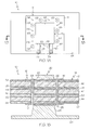
- FIG. 1A is a top view of an electronic circuit board assembly including a power electronic device and a multi-layer circuit board incorporating a thermal conduction structure according to this invention
- FIG. 1B is a cross-sectional view of the an electronic circuit board assembly of FIG. 1A taken along lines 1B-1B of FIG. 1A ;
- FIG. 2 is an isometric illustration of a thermal conduction structure according to this invention, with core insulative layers of the structure removed to reveal the thermal conduction paths.
- the present invention is directed to a multi-layer thermal conduction structure designed into a multi-layer circuit board or substrate.
- a power electronic device is mounted on one side of the thermal conduction structure, and a heatsink is affixed to the other side of the thermal conduction structure.
- the purpose of the thermal conduction structure is to thermally couple the power electronic device to the heatsink while electrically isolating the power electronic device from the heatsink.
- the thermal conduction structure is illustrated in the context of a multi-layer woven glass (FR4) circuit board, but it will be appreciated that the structure could alternately be implemented in a multi-layer ceramic circuit board.
- FR4 multi-layer woven glass
- the reference numeral 10 generally designates an electronic circuit board assembly incorporating a multi-layer thermal conduction structure 12 according to this invention.
- Thermal conduction structure 12 is designed into a multi-layer circuit board 14 (also referred to herein as a substrate) of conventional construction, resulting in exposed upper and lower copper pads 16 and 18.
- a power electronic device 20 having an exposed metal base 22 is soldered or otherwise thermally affixed to a central region of the upper copper pad 16, and the pedestal 24 of a metal heatsink 26 is soldered or otherwise thermally affixed to a central region the lower copper pad 18 opposite the device 20.
- a thin layer 25 of solder may be used to provide a high thermal conductivity joint between copper pad 18 and pedestal 24.
- the metal base 22 forms one terminal of the device 20, and the other terminals 28 and 30 of device 20 extend beyond the perimeter of thermal conduction structure 12 where they are soldered to respective pads 32 and 34.
- the thermal conduction structure 12 comprises a number of alternatingly insulative and conductive layers between the upper and lower copper pads 16 and 18 that insulate upper copper pad 16 from lower copper pad 18 while providing thermal conduction between adjacent layers to transfer heat dissipated by the device 20 to the metal pedestal 24.
- the reference numerals 40-52 designate the insulative layers
- the reference numerals 54-64 designate the conductive layers.
- Insulative layers 40-44 (also referred to herein as core layers) and conductive layers 54-64 are defined by a three-sheet stack of copper-clad epoxy-impregnated woven glass circuit board material such as FR4.
- conductive layers 54 and 56 are bonded to opposing faces of the top core layer 40; conductive layers 58 and 60 are bonded to opposing faces of the middle core layer 42; and conductive layers 62 and 64 are bonded to opposing faces of the bottom core layer 44.
- the core layers 40-44 will each have a thickness of 0.010 inch, for example, and the copper layers 54-64 will each have a thickness of 0.0028 inch, for example.
- the insulative layers 46-52 electrically isolate adjacent conductive layers 16, 54-64 and 18.
- insulative layer 46 is disposed between upper copper pad 16 and conductive layer 54; insulative layer 48 is disposed between conductive layers 56 and 58; insulative layer 50 is disposed between conductive layers 60 and 62; and insulative layer 52 is disposed between conductive layer 64 and lower copper pad 18.
- the insulative layers 46-52 are preferably formed of pre-impregnated woven glass material (i.e., pre-preg FR4) having a thickness of 0.003 inch, for example, and serve as a thermal bridge between respective adjacent conductive layers.
- Thermal conduction structure 12 additionally includes an array of copper-lined vias 66 and 68 that are located in a marginal area beyond the footprint of the device 20, and that extend vertically through the entire structure.
- the vias 66 are joined to the upper copper pad 16 and conductive layers 56, 60 and 64, but are separated from the lower copper pad 18 and conductive layers 54, 58 and 62.
- the vias 68 are separated from upper copper pad 16 and conductive layers 56, 60 and 64, but are joined to lower copper pad 18 and conductive layers 54, 58 and 62. This preserves the electrical isolation between upper and lower pads 16 and 18, while providing vertical thermal conduction paths between alternating conductive layers.
- thermal conduction structure 12 can be designed into (and replicated in) a multi-layer circuit board using conventional circuit board manufacturing techniques such as photo-etching the copper layers bonded to core layers 40-44, drilling vertically through the layered assembly to locate the vias 66-68, and copper-plating the drilled openings to form the vias 66-68.
- the conductive layers 54, 58, 62 and 18 are circularly etched to ensure that they remain electrically isolated from the vias 66.
- the conductive layers 16, 56, 60 and 64 are circularly etched to ensure that they remain electrically isolated from the vias 68, as seen in the illustration of FIG. 2 where the core layers 40-44 have been omitted to reveal the primary thermal conduction paths between upper and lower pads 16 and 18.
- the thermal conduction structure 12 of present invention provides a reliable and cost-effective way of transferring heat from a power electronic device to a heatsink while electrically isolating the power electronic device from the heatsink.
- Heat applied to upper pad 16 by the device 20 is successively transferred to the intermediate copper layers 54-64 and 18 through the thin insulative thermal bridge layers 46-52 and the vias 66-68, and is then transferred to the metal pedestal 24 through the solder or conductive adhesive layer 25 joining lower pad 18 to heatsink 26.
- Testing has indicated that the described thermal conduction structure 12 thermally outperforms known via structures, while avoiding the expense associated with providing a special insulative interface between the circuit board and the heatsink.
Landscapes
- Engineering & Computer Science (AREA)
- Microelectronics & Electronic Packaging (AREA)
- Physics & Mathematics (AREA)
- Thermal Sciences (AREA)
- Production Of Multi-Layered Print Wiring Board (AREA)
Abstract
Description
- The present invention relates to an electronic circuit board assembly including a power electronic device mounted on a multi-layer circuit board, and more particularly to an electrically isolated thermal conduction structure integrated into the multi-layer circuit board for dissipating heat generated by the power electronic device.
- Various thermal conduction structures have been used to dissipate heat generated by the power electronic devices of electronic circuit board assemblies. A common approach is to attach a heatsink to the circuit board substrate opposite the power electronic devices, and to incorporate thermal vias into the circuit board for thermally coupling the power devices to the heatsink. While the thermal via approach can be effectively used in certain applications, it is frequently necessary to electrically isolate the power electronic devices from the heatsink by depositing a layer of special insulating material between the circuit board and the heatsink. This not only increases the cost of the circuit board assembly, but also reduces thermal coupling of the circuit board to the heatsink. Accordingly, what is needed is a circuit board having an electrically isolated thermal conduction structure that is inexpensive to manufacture and that provides improved thermal coupling.
- The present invention is directed to an improved thermal conduction structure integrated into a multi-layer circuit board for thermally coupling a power electronic device to a heatsink while providing electrical isolation between the power electronic device and the heatsink. The thermal conduction structure includes a stack of alternatingly insulative and conductive layers, a first set of vertical vias that thermally and electrically join the power electronic device to a first set of conductive layers, and a second set of vertical vias that thermally and electrically join the heatsink to a second set of conductive layers that are interleaved with the first set of conductive layers.
-
FIG. 1A is a top view of an electronic circuit board assembly including a power electronic device and a multi-layer circuit board incorporating a thermal conduction structure according to this invention; -
FIG. 1B is a cross-sectional view of the an electronic circuit board assembly ofFIG. 1A taken alonglines 1B-1B ofFIG. 1A ; and -
FIG. 2 is an isometric illustration of a thermal conduction structure according to this invention, with core insulative layers of the structure removed to reveal the thermal conduction paths. - In general, the present invention is directed to a multi-layer thermal conduction structure designed into a multi-layer circuit board or substrate. A power electronic device is mounted on one side of the thermal conduction structure, and a heatsink is affixed to the other side of the thermal conduction structure. The purpose of the thermal conduction structure is to thermally couple the power electronic device to the heatsink while electrically isolating the power electronic device from the heatsink. The thermal conduction structure is illustrated in the context of a multi-layer woven glass (FR4) circuit board, but it will be appreciated that the structure could alternately be implemented in a multi-layer ceramic circuit board.
- Referring to
FIGS. 1A-1B , thereference numeral 10 generally designates an electronic circuit board assembly incorporating a multi-layerthermal conduction structure 12 according to this invention.Thermal conduction structure 12 is designed into a multi-layer circuit board 14 (also referred to herein as a substrate) of conventional construction, resulting in exposed upper andlower copper pads electronic device 20 having an exposedmetal base 22 is soldered or otherwise thermally affixed to a central region of theupper copper pad 16, and thepedestal 24 of ametal heatsink 26 is soldered or otherwise thermally affixed to a central region thelower copper pad 18 opposite thedevice 20. For example, athin layer 25 of solder may be used to provide a high thermal conductivity joint betweencopper pad 18 andpedestal 24. In the illustration, themetal base 22 forms one terminal of thedevice 20, and theother terminals device 20 extend beyond the perimeter ofthermal conduction structure 12 where they are soldered torespective pads - As depicted in the cross-sectional view of
FIG. 1B , thethermal conduction structure 12 comprises a number of alternatingly insulative and conductive layers between the upper andlower copper pads upper copper pad 16 fromlower copper pad 18 while providing thermal conduction between adjacent layers to transfer heat dissipated by thedevice 20 to themetal pedestal 24. The reference numerals 40-52 designate the insulative layers, while the reference numerals 54-64 designate the conductive layers. Insulative layers 40-44 (also referred to herein as core layers) and conductive layers 54-64 are defined by a three-sheet stack of copper-clad epoxy-impregnated woven glass circuit board material such as FR4. That is,conductive layers top core layer 40;conductive layers middle core layer 42; andconductive layers bottom core layer 44. Typically, the core layers 40-44 will each have a thickness of 0.010 inch, for example, and the copper layers 54-64 will each have a thickness of 0.0028 inch, for example. The insulative layers 46-52 electrically isolate adjacentconductive layers 16, 54-64 and 18. Specifically,insulative layer 46 is disposed betweenupper copper pad 16 andconductive layer 54;insulative layer 48 is disposed betweenconductive layers insulative layer 50 is disposed betweenconductive layers insulative layer 52 is disposed betweenconductive layer 64 andlower copper pad 18. The insulative layers 46-52 are preferably formed of pre-impregnated woven glass material (i.e., pre-preg FR4) having a thickness of 0.003 inch, for example, and serve as a thermal bridge between respective adjacent conductive layers. -
Thermal conduction structure 12 additionally includes an array of copper-linedvias device 20, and that extend vertically through the entire structure. Thevias 66 are joined to theupper copper pad 16 andconductive layers lower copper pad 18 andconductive layers vias 68 are separated fromupper copper pad 16 andconductive layers copper pad 18 andconductive layers lower pads - It will be appreciated that the above-described
thermal conduction structure 12 can be designed into (and replicated in) a multi-layer circuit board using conventional circuit board manufacturing techniques such as photo-etching the copper layers bonded to core layers 40-44, drilling vertically through the layered assembly to locate the vias 66-68, and copper-plating the drilled openings to form the vias 66-68. For example, theconductive layers vias 66. Similarly, theconductive layers vias 68, as seen in the illustration ofFIG. 2 where the core layers 40-44 have been omitted to reveal the primary thermal conduction paths between upper andlower pads - In summary, the
thermal conduction structure 12 of present invention provides a reliable and cost-effective way of transferring heat from a power electronic device to a heatsink while electrically isolating the power electronic device from the heatsink. Heat applied toupper pad 16 by thedevice 20 is successively transferred to the intermediate copper layers 54-64 and 18 through the thin insulative thermal bridge layers 46-52 and the vias 66-68, and is then transferred to themetal pedestal 24 through the solder or conductiveadhesive layer 25 joininglower pad 18 toheatsink 26. Testing has indicated that the describedthermal conduction structure 12 thermally outperforms known via structures, while avoiding the expense associated with providing a special insulative interface between the circuit board and the heatsink. - While the invention has been described with respect to the illustrated embodiment, it is recognized that numerous modifications and variations in addition to those mentioned herein will occur to those skilled in the art. For example, the shape, thickness, number of layers and material composition may be different than shown herein, one or more blind vias may be included in the structure, and so on. Accordingly, it is intended that the invention not be limited to the disclosed embodiment, but that it have the full scope permitted by the language of the following claims.
Claims (8)
- A multi-layer electrically isolated thermal conduction structure (12) for thermally coupling a power electronic device (20) mounted on a first side of the structure (12) to heatsink (24) thermally coupled to a second side of the structure (12), comprising:a stack of alternatingly insulative and conductive layers (40-52; 16-18, 54-64) disposed between the power electronic device (20) and the heatsink (24), including a first set of conductive layers (16, 56, 60, 64) thermally and electrically coupled to the power electronic device (20), and a second set of conductive layers (54, 58, 62, 18) thermally and electrically coupled to the heatsink (24), the second set of conductive layers (54, 58, 62, 18) being interleaved with the first set of conductive layers (16, 56, 60, 64) but electrically isolated from the first set of conductive layers (16, 56, 60, 64) and the power electronic device (20) by the insulative layers (40-52).
- The multi-layer electrically isolated thermal conduction structure of claim 1, further comprising:a first set of conductive vias (66) that thermally and electrically join the first set of conductive layers (16, 56, 60, 64) to the power electronic device (20); anda second set of conductive vias (68) that thermally and electrically join the second set of conductive layers (54, 58, 62, 18) to the heatsink (24).
- The multi-layer electrically isolated thermal conduction structure of claim 2, where:the first set of conductive vias (66) is electrically isolated from the second set of conductive layers (54, 58, 62, 18); andthe second set of conductive vias (68) is electrically isolated from the first set of conductive layers (16, 56, 60, 64).
- The multi-layer electrically isolated thermal conduction structure of claim 1, where:the stack of alternatingly insulative and conductive layers (40-52; 16-18, 54-64) are designed into a multi-layer circuit board (14).
- The multi-layer electrically isolated thermal conduction structure of claim 1, where:the insulative layers (40-52) include a set of core layers (40-44) to which the conductive layers (54-64) are affixed, and a set of thermal bridge layers (46-52) disposed between adjacently disposed conductive layers (16, 54; 56, 58; 60, 62; 64, 18).
- The multi-layer electrically isolated thermal conduction structure of claim 5, where:the core layers (40-44) are formed of epoxy impregnated woven glass material; andthe thermal bridge layers (46-52) are formed of pre-impregnated woven glass material.
- The multi-layer electrically isolated thermal conduction structure of claim 6, where:the thermal bridge layers (46-52) each have a thickness of approximately .003-.004 inch.
- The multi-layer electrically isolated thermal conduction structure of claim 1, further comprising:a solder layer (25) thermally coupling the heatsink (24) to the second side of the structure (12).
Applications Claiming Priority (1)
| Application Number | Priority Date | Filing Date | Title |
|---|---|---|---|
| US11/824,019 US7808788B2 (en) | 2007-06-29 | 2007-06-29 | Multi-layer electrically isolated thermal conduction structure for a circuit board assembly |
Publications (1)
| Publication Number | Publication Date |
|---|---|
| EP2009966A1 true EP2009966A1 (en) | 2008-12-31 |
Family
ID=39764690
Family Applications (1)
| Application Number | Title | Priority Date | Filing Date |
|---|---|---|---|
| EP08157557A Withdrawn EP2009966A1 (en) | 2007-06-29 | 2008-06-04 | Multi-layer electrically isolated thermal conduction structure for a circuit board assembly |
Country Status (2)
| Country | Link |
|---|---|
| US (1) | US7808788B2 (en) |
| EP (1) | EP2009966A1 (en) |
Cited By (1)
| Publication number | Priority date | Publication date | Assignee | Title |
|---|---|---|---|---|
| EP2317272A3 (en) * | 2009-10-28 | 2013-05-15 | Tai-Her Yang | Thermal conduction device having a layered structure with different thermal characteristics of the layers |
Families Citing this family (27)
| Publication number | Priority date | Publication date | Assignee | Title |
|---|---|---|---|---|
| JP2010238821A (en) * | 2009-03-30 | 2010-10-21 | Sony Corp | Multilayer wiring board, stack structure sensor package and manufacturing method thereof |
| WO2010146652A1 (en) * | 2009-06-15 | 2010-12-23 | 富士通オプティカルコンポーネンツ株式会社 | Optical module |
| KR101084900B1 (en) * | 2009-11-23 | 2011-11-17 | 삼성에스디아이 주식회사 | Secondary Battery and Circuit Board Assembly Used Thereof |
| US8009429B1 (en) | 2010-03-22 | 2011-08-30 | Honeywell International Inc. | Electrical component thermal management |
| JP2011249520A (en) * | 2010-05-26 | 2011-12-08 | Mitsubishi Electric Corp | Electronic control device |
| US8957316B2 (en) * | 2010-09-10 | 2015-02-17 | Honeywell International Inc. | Electrical component assembly for thermal transfer |
| JP5533787B2 (en) | 2011-06-09 | 2014-06-25 | 株式会社豊田自動織機 | Heat dissipation device |
| JP6021504B2 (en) * | 2012-08-08 | 2016-11-09 | キヤノン株式会社 | Printed wiring board, printed circuit board, and printed circuit board manufacturing method |
| FR2999479B1 (en) * | 2012-12-19 | 2015-01-30 | Valeo Systemes Thermiques | VENTILATION DEVICE FOR VENTILATION, HEATING AND / OR AIR CONDITIONING INSTALLATION |
| FR2999864A1 (en) * | 2012-12-19 | 2014-06-20 | Valeo Systemes Thermiques | COOLING DEVICE FOR PRINTED CIRCUIT BOARD |
| USD729808S1 (en) * | 2013-03-13 | 2015-05-19 | Nagrastar Llc | Smart card interface |
| USD759022S1 (en) * | 2013-03-13 | 2016-06-14 | Nagrastar Llc | Smart card interface |
| USD758372S1 (en) * | 2013-03-13 | 2016-06-07 | Nagrastar Llc | Smart card interface |
| US10366935B2 (en) | 2013-04-09 | 2019-07-30 | Otis Elevator Company | Architecture of drive unit employing gallium nitride switches |
| WO2016048676A1 (en) * | 2014-09-24 | 2016-03-31 | Hiq Solar, Inc. | Transistor thermal and emi management solution for fast edge rate environment |
| USD780763S1 (en) * | 2015-03-20 | 2017-03-07 | Nagrastar Llc | Smart card interface |
| USD864968S1 (en) | 2015-04-30 | 2019-10-29 | Echostar Technologies L.L.C. | Smart card interface |
| DE102015219565A1 (en) * | 2015-10-09 | 2017-04-13 | Continental Automotive Gmbh | Heat sink, method for manufacturing a heat sink and electronic module with a heat sink |
| JP6477567B2 (en) * | 2016-03-30 | 2019-03-06 | 株式会社オートネットワーク技術研究所 | Circuit structure |
| CN110637361B (en) * | 2017-05-22 | 2024-04-19 | 索尼互动娱乐股份有限公司 | Electronic equipment |
| DE202017106861U1 (en) * | 2017-11-10 | 2018-01-03 | Valeo Thermal Commercial Vehicles Germany GmbH | electronics package |
| DE102017220417A1 (en) * | 2017-11-16 | 2019-05-16 | Continental Automotive Gmbh | Electronic module |
| FR3084960B1 (en) * | 2018-08-07 | 2020-10-23 | Safran Electrical & Power | ELECTRICAL POWER CIRCUIT FOR ELECTRIC POWER CONVERTER |
| US11545297B2 (en) * | 2019-06-06 | 2023-01-03 | Toyota Motor Engineering & Manufacturing North America, Inc. | Functionally graded thermal vias for inductor winding heat flow control |
| WO2022081335A1 (en) * | 2020-10-13 | 2022-04-21 | Qorvo Us, Inc. | Laminate substrate with embedded multi-layered heat slug |
| CN116321685A (en) * | 2023-02-24 | 2023-06-23 | 华为数字能源技术有限公司 | Metal Substrates and Power Devices |
| US20260052621A1 (en) * | 2024-08-13 | 2026-02-19 | Stmicroelectronics International N.V. | Printed circuit board heat exchanger and associated method |
Citations (5)
| Publication number | Priority date | Publication date | Assignee | Title |
|---|---|---|---|---|
| GB1220370A (en) * | 1968-08-13 | 1971-01-27 | Litton Industries Inc | Electrical circuit boards |
| US4628407A (en) * | 1983-04-22 | 1986-12-09 | Cray Research, Inc. | Circuit module with enhanced heat transfer and distribution |
| DE4335946A1 (en) * | 1993-10-21 | 1995-04-27 | Bosch Gmbh Robert | Arrangement consisting of a printed circuit board |
| WO1999057951A1 (en) * | 1998-04-30 | 1999-11-11 | Telefonaktiebolaget Lm Ericsson (Publ) | A printed circuit board and a method of processing printed circuit boards |
| US20060220227A1 (en) * | 2005-04-04 | 2006-10-05 | Data Device Corporation | High density integrated circuit having multiple chips and employing a ball grid array (BGA) and method for making same |
Family Cites Families (42)
| Publication number | Priority date | Publication date | Assignee | Title |
|---|---|---|---|---|
| US4739448A (en) * | 1984-06-25 | 1988-04-19 | Magnavox Government And Industrial Electronics Company | Microwave multiport multilayered integrated circuit chip carrier |
| US4729061A (en) * | 1985-04-29 | 1988-03-01 | Advanced Micro Devices, Inc. | Chip on board package for integrated circuit devices using printed circuit boards and means for conveying the heat to the opposite side of the package from the chip mounting side to permit the heat to dissipate therefrom |
| US4810563A (en) * | 1986-03-14 | 1989-03-07 | The Bergquist Company | Thermally conductive, electrically insulative laminate |
| US4731701A (en) * | 1987-05-12 | 1988-03-15 | Fairchild Semiconductor Corporation | Integrated circuit package with thermal path layers incorporating staggered thermal vias |
| JP2760829B2 (en) * | 1989-01-13 | 1998-06-04 | 株式会社日立製作所 | Electronic substrate |
| US5045642A (en) * | 1989-04-20 | 1991-09-03 | Satosen, Co., Ltd. | Printed wiring boards with superposed copper foils cores |
| US4964019A (en) * | 1989-12-27 | 1990-10-16 | Ag Communication Systems Corporation | Multilayer bonding and cooling of integrated circuit devices |
| US5506755A (en) * | 1992-03-11 | 1996-04-09 | Kabushiki Kaisha Toshiba | Multi-layer substrate |
| US5258887A (en) * | 1992-06-15 | 1993-11-02 | Eaton Corporation | Electrical device cooling system using a heat sink attached to a circuit board containing heat conductive layers and channels |
| US5352926A (en) * | 1993-01-04 | 1994-10-04 | Motorola, Inc. | Flip chip package and method of making |
| US5386339A (en) * | 1993-07-29 | 1995-01-31 | Hughes Aircraft Company | Monolithic microelectronic circuit package including low-temperature-cofired-ceramic (LTCC) tape dielectric structure and in-situ heat sink |
| US5467251A (en) * | 1993-10-08 | 1995-11-14 | Northern Telecom Limited | Printed circuit boards and heat sink structures |
| US6031723A (en) * | 1994-08-18 | 2000-02-29 | Allen-Bradley Company, Llc | Insulated surface mount circuit board construction |
| US6200407B1 (en) * | 1994-08-18 | 2001-03-13 | Rockwell Technologies, Llc | Method of making a multilayer circuit board having a window exposing an enhanced conductive layer for use as an insulated mounting area |
| US5646373A (en) * | 1994-09-02 | 1997-07-08 | Caterpillar Inc. | Apparatus for improving the power dissipation of a semiconductor device |
| US5625227A (en) * | 1995-01-18 | 1997-04-29 | Dell Usa, L.P. | Circuit board-mounted IC package cooling apparatus |
| JPH0955459A (en) * | 1995-06-06 | 1997-02-25 | Seiko Epson Corp | Semiconductor device |
| US5616888A (en) * | 1995-09-29 | 1997-04-01 | Allen-Bradley Company, Inc. | Rigid-flex circuit board having a window for an insulated mounting area |
| US5721454A (en) * | 1995-12-20 | 1998-02-24 | Intel Corporation | Integrated circuit package with a plurality of vias that are electrically connected to an internal ground plane and thermally connected to an external heat slug |
| US5708566A (en) * | 1996-10-31 | 1998-01-13 | Motorola, Inc. | Solder bonded electronic module |
| JPH1140901A (en) * | 1997-07-23 | 1999-02-12 | Sharp Corp | Circuit board |
| US6201701B1 (en) * | 1998-03-11 | 2001-03-13 | Kimball International, Inc. | Integrated substrate with enhanced thermal characteristics |
| US6058013A (en) * | 1998-07-02 | 2000-05-02 | Motorola Inc. | Molded housing with integral heatsink |
| US6191477B1 (en) * | 1999-02-17 | 2001-02-20 | Conexant Systems, Inc. | Leadless chip carrier design and structure |
| TW413874B (en) * | 1999-04-12 | 2000-12-01 | Siliconware Precision Industries Co Ltd | BGA semiconductor package having exposed heat dissipation layer and its manufacturing method |
| US6137064A (en) * | 1999-06-11 | 2000-10-24 | Teradyne, Inc. | Split via surface mount connector and related techniques |
| US6373717B1 (en) * | 1999-07-02 | 2002-04-16 | International Business Machines Corporation | Electronic package with high density interconnect layer |
| US6351393B1 (en) * | 1999-07-02 | 2002-02-26 | International Business Machines Corporation | Electronic package for electronic components and method of making same |
| DE19950026B4 (en) * | 1999-10-09 | 2010-11-11 | Robert Bosch Gmbh | The power semiconductor module |
| EP1178594B1 (en) * | 2000-08-01 | 2009-08-12 | Mitsubishi Denki Kabushiki Kaisha | Electronic apparatus provided with an electronic circuit substrate |
| US6696643B2 (en) * | 2000-08-01 | 2004-02-24 | Mitsubishi Denki Kabushiki Kaisha | Electronic apparatus |
| US6477054B1 (en) * | 2000-08-10 | 2002-11-05 | Tektronix, Inc. | Low temperature co-fired ceramic substrate structure having a capacitor and thermally conductive via |
| KR100391093B1 (en) * | 2001-01-04 | 2003-07-12 | 삼성전자주식회사 | Ball Grid Array package mounting heat sink |
| US6521842B2 (en) * | 2001-06-20 | 2003-02-18 | International Business Machines Corporation | Hybrid surface mount and pin thru hole circuit board |
| JP2003289191A (en) * | 2002-03-28 | 2003-10-10 | Denso Corp | Electronic control unit |
| US7138711B2 (en) * | 2002-06-17 | 2006-11-21 | Micron Technology, Inc. | Intrinsic thermal enhancement for FBGA package |
| US20040037044A1 (en) * | 2002-08-21 | 2004-02-26 | Alexander Cook | Heat sink for surface mounted power devices |
| US6930885B2 (en) * | 2002-12-23 | 2005-08-16 | Eastman Kodak Company | Densely packed electronic assemblage with heat removing element |
| JP4457694B2 (en) * | 2003-05-19 | 2010-04-28 | 株式会社デンソー | Heat dissipation structure for electronic components |
| US7269017B2 (en) * | 2004-11-19 | 2007-09-11 | Delphi Technologies, Inc. | Thermal management of surface-mount circuit devices on laminate ceramic substrate |
| JP2006261255A (en) * | 2005-03-16 | 2006-09-28 | Matsushita Electric Ind Co Ltd | Semiconductor device |
| US7586191B2 (en) * | 2005-08-11 | 2009-09-08 | Hall David R | Integrated circuit apparatus with heat spreader |
-
2007
- 2007-06-29 US US11/824,019 patent/US7808788B2/en not_active Expired - Fee Related
-
2008
- 2008-06-04 EP EP08157557A patent/EP2009966A1/en not_active Withdrawn
Patent Citations (5)
| Publication number | Priority date | Publication date | Assignee | Title |
|---|---|---|---|---|
| GB1220370A (en) * | 1968-08-13 | 1971-01-27 | Litton Industries Inc | Electrical circuit boards |
| US4628407A (en) * | 1983-04-22 | 1986-12-09 | Cray Research, Inc. | Circuit module with enhanced heat transfer and distribution |
| DE4335946A1 (en) * | 1993-10-21 | 1995-04-27 | Bosch Gmbh Robert | Arrangement consisting of a printed circuit board |
| WO1999057951A1 (en) * | 1998-04-30 | 1999-11-11 | Telefonaktiebolaget Lm Ericsson (Publ) | A printed circuit board and a method of processing printed circuit boards |
| US20060220227A1 (en) * | 2005-04-04 | 2006-10-05 | Data Device Corporation | High density integrated circuit having multiple chips and employing a ball grid array (BGA) and method for making same |
Cited By (1)
| Publication number | Priority date | Publication date | Assignee | Title |
|---|---|---|---|---|
| EP2317272A3 (en) * | 2009-10-28 | 2013-05-15 | Tai-Her Yang | Thermal conduction device having a layered structure with different thermal characteristics of the layers |
Also Published As
| Publication number | Publication date |
|---|---|
| US20090002950A1 (en) | 2009-01-01 |
| US7808788B2 (en) | 2010-10-05 |
Similar Documents
| Publication | Publication Date | Title |
|---|---|---|
| US7808788B2 (en) | Multi-layer electrically isolated thermal conduction structure for a circuit board assembly | |
| EP3355349B1 (en) | Efficient heat removal from component carrier with embedded diode | |
| US7269017B2 (en) | Thermal management of surface-mount circuit devices on laminate ceramic substrate | |
| CN103339726B (en) | Electronic device, method for producing the latter, and printed circuit board comprising electronic device | |
| CN206976318U (en) | Module | |
| CN102017135B (en) | Substrate-mounted circuit module comprising components in a plurality of contact planes | |
| JP2003101243A (en) | Multilayer wiring board and semiconductor device | |
| US20070010086A1 (en) | Circuit board with a through hole wire and manufacturing method thereof | |
| EP2577724B1 (en) | Method of manufacturing printed circuit board | |
| US20080017402A1 (en) | Substrate module with high thermal conductivity and its fabrication method of same | |
| US9860990B1 (en) | Circuit board structure with chips embedded therein and manufacturing method thereof | |
| JP2003509872A (en) | Printed circuit board assembly | |
| JP2010511289A (en) | Light emitting diode with integrated thermal via | |
| TW201507556A (en) | Thermally enhanced wiring board with thermal pad and electrical post | |
| JP5093104B2 (en) | Interposer with built-in passive components | |
| US7915541B2 (en) | Multilayer interconnection substrate and manufacturing method therefor | |
| JPH06291165A (en) | Flip chip connection structure | |
| KR102553052B1 (en) | PCB of heat dissipation type, and method of the same | |
| JPH08236940A (en) | Multilayer wiring board | |
| CN116867161A (en) | Circuit board with embedded copper component and preparation method thereof | |
| JP4797676B2 (en) | Insulated heat transfer structure, power module substrate, and method of manufacturing insulated heat transfer structure | |
| JP2001077290A (en) | Three-dimensional electronic component module, three-dimensional electronic component module, and method of manufacturing the same | |
| JP2010258335A (en) | Component built-in wiring board, method of manufacturing component built-in wiring board | |
| JP5708489B2 (en) | Semiconductor device having metallic power supply side and ground side reinforcing members insulated from each other | |
| CN113260137A (en) | Printed circuit board, circuit board assembly and power supply device |
Legal Events
| Date | Code | Title | Description |
|---|---|---|---|
| PUAI | Public reference made under article 153(3) epc to a published international application that has entered the european phase |
Free format text: ORIGINAL CODE: 0009012 |
|
| AK | Designated contracting states |
Kind code of ref document: A1 Designated state(s): AT BE BG CH CY CZ DE DK EE ES FI FR GB GR HR HU IE IS IT LI LT LU LV MC MT NL NO PL PT RO SE SI SK TR |
|
| AX | Request for extension of the european patent |
Extension state: AL BA MK RS |
|
| 17P | Request for examination filed |
Effective date: 20090630 |
|
| AKX | Designation fees paid |
Designated state(s): AT BE BG CH CY CZ DE DK EE ES FI FR GB GR HR HU IE IS IT LI LT LU LV MC MT NL NO PL PT RO SE SI SK TR |
|
| 17Q | First examination report despatched |
Effective date: 20090908 |
|
| STAA | Information on the status of an ep patent application or granted ep patent |
Free format text: STATUS: THE APPLICATION IS DEEMED TO BE WITHDRAWN |
|
| 18D | Application deemed to be withdrawn |
Effective date: 20100319 |