EP2009480A2 - High power bimorph wave-front correction mirror - Google Patents
High power bimorph wave-front correction mirror Download PDFInfo
- Publication number
- EP2009480A2 EP2009480A2 EP08251940A EP08251940A EP2009480A2 EP 2009480 A2 EP2009480 A2 EP 2009480A2 EP 08251940 A EP08251940 A EP 08251940A EP 08251940 A EP08251940 A EP 08251940A EP 2009480 A2 EP2009480 A2 EP 2009480A2
- Authority
- EP
- European Patent Office
- Prior art keywords
- mirror
- actuator
- disk
- wave
- approximately
- Prior art date
- Legal status (The legal status is an assumption and is not a legal conclusion. Google has not performed a legal analysis and makes no representation as to the accuracy of the status listed.)
- Withdrawn
Links
- 238000012937 correction Methods 0.000 title claims abstract description 19
- 238000000034 method Methods 0.000 claims abstract description 27
- 230000003287 optical effect Effects 0.000 claims abstract description 16
- 239000000919 ceramic Substances 0.000 claims abstract description 8
- 238000004519 manufacturing process Methods 0.000 claims abstract description 5
- 238000002310 reflectometry Methods 0.000 claims description 24
- 239000000853 adhesive Substances 0.000 claims description 14
- 230000001070 adhesive effect Effects 0.000 claims description 14
- 239000011248 coating agent Substances 0.000 claims description 12
- 238000000576 coating method Methods 0.000 claims description 12
- 239000004593 Epoxy Substances 0.000 claims description 11
- 230000004075 alteration Effects 0.000 claims description 4
- 230000000737 periodic effect Effects 0.000 claims description 4
- 230000004044 response Effects 0.000 claims description 3
- 230000001351 cycling effect Effects 0.000 claims description 2
- 238000004140 cleaning Methods 0.000 claims 1
- 238000005498 polishing Methods 0.000 claims 1
- 239000000463 material Substances 0.000 description 17
- KFZMGEQAYNKOFK-UHFFFAOYSA-N Isopropanol Chemical compound CC(C)O KFZMGEQAYNKOFK-UHFFFAOYSA-N 0.000 description 16
- CSCPPACGZOOCGX-UHFFFAOYSA-N Acetone Chemical compound CC(C)=O CSCPPACGZOOCGX-UHFFFAOYSA-N 0.000 description 13
- 239000007787 solid Substances 0.000 description 7
- OKKJLVBELUTLKV-UHFFFAOYSA-N Methanol Chemical compound OC OKKJLVBELUTLKV-UHFFFAOYSA-N 0.000 description 6
- 239000011324 bead Substances 0.000 description 6
- 239000000203 mixture Substances 0.000 description 6
- 230000008859 change Effects 0.000 description 5
- 238000009826 distribution Methods 0.000 description 5
- 239000011521 glass Substances 0.000 description 5
- 230000008569 process Effects 0.000 description 5
- 238000005452 bending Methods 0.000 description 4
- 238000012512 characterization method Methods 0.000 description 4
- 150000001875 compounds Chemical class 0.000 description 4
- 239000004744 fabric Substances 0.000 description 4
- 238000002156 mixing Methods 0.000 description 4
- 238000012360 testing method Methods 0.000 description 4
- 229910001374 Invar Inorganic materials 0.000 description 3
- VYPSYNLAJGMNEJ-UHFFFAOYSA-N Silicium dioxide Chemical compound O=[Si]=O VYPSYNLAJGMNEJ-UHFFFAOYSA-N 0.000 description 3
- 230000000694 effects Effects 0.000 description 3
- 230000004907 flux Effects 0.000 description 3
- 238000010438 heat treatment Methods 0.000 description 3
- 238000010943 off-gassing Methods 0.000 description 3
- 238000005476 soldering Methods 0.000 description 3
- 230000008901 benefit Effects 0.000 description 2
- 230000005540 biological transmission Effects 0.000 description 2
- 230000000875 corresponding effect Effects 0.000 description 2
- 230000008878 coupling Effects 0.000 description 2
- 238000010168 coupling process Methods 0.000 description 2
- 238000005859 coupling reaction Methods 0.000 description 2
- 239000007788 liquid Substances 0.000 description 2
- 229920000647 polyepoxide Polymers 0.000 description 2
- 239000004848 polyfunctional curative Substances 0.000 description 2
- 238000005086 pumping Methods 0.000 description 2
- 229920005989 resin Polymers 0.000 description 2
- 239000011347 resin Substances 0.000 description 2
- 229920002379 silicone rubber Polymers 0.000 description 2
- 239000004945 silicone rubber Substances 0.000 description 2
- 229910000679 solder Inorganic materials 0.000 description 2
- 239000000725 suspension Substances 0.000 description 2
- 238000001069 Raman spectroscopy Methods 0.000 description 1
- 239000004809 Teflon Substances 0.000 description 1
- 230000001594 aberrant effect Effects 0.000 description 1
- 230000009471 action Effects 0.000 description 1
- 230000003044 adaptive effect Effects 0.000 description 1
- 239000012790 adhesive layer Substances 0.000 description 1
- XAGFODPZIPBFFR-UHFFFAOYSA-N aluminium Chemical compound [Al] XAGFODPZIPBFFR-UHFFFAOYSA-N 0.000 description 1
- 229910052782 aluminium Inorganic materials 0.000 description 1
- 238000013459 approach Methods 0.000 description 1
- 238000006243 chemical reaction Methods 0.000 description 1
- 238000001816 cooling Methods 0.000 description 1
- 230000002596 correlated effect Effects 0.000 description 1
- 230000005574 cross-species transmission Effects 0.000 description 1
- 230000001419 dependent effect Effects 0.000 description 1
- 238000013461 design Methods 0.000 description 1
- 230000005489 elastic deformation Effects 0.000 description 1
- 229920001971 elastomer Polymers 0.000 description 1
- 238000005516 engineering process Methods 0.000 description 1
- 229920006332 epoxy adhesive Polymers 0.000 description 1
- 125000003700 epoxy group Chemical group 0.000 description 1
- 239000003822 epoxy resin Substances 0.000 description 1
- 230000005284 excitation Effects 0.000 description 1
- 230000001815 facial effect Effects 0.000 description 1
- 239000000945 filler Substances 0.000 description 1
- 238000011010 flushing procedure Methods 0.000 description 1
- -1 for example Chemical class 0.000 description 1
- 238000009472 formulation Methods 0.000 description 1
- 230000006870 function Effects 0.000 description 1
- 239000005350 fused silica glass Substances 0.000 description 1
- 238000007731 hot pressing Methods 0.000 description 1
- 238000010348 incorporation Methods 0.000 description 1
- 230000010354 integration Effects 0.000 description 1
- 238000002955 isolation Methods 0.000 description 1
- 238000013507 mapping Methods 0.000 description 1
- 230000013011 mating Effects 0.000 description 1
- 238000005259 measurement Methods 0.000 description 1
- 230000007246 mechanism Effects 0.000 description 1
- 239000004005 microsphere Substances 0.000 description 1
- 238000012986 modification Methods 0.000 description 1
- 230000004048 modification Effects 0.000 description 1
- 238000012544 monitoring process Methods 0.000 description 1
- 239000005304 optical glass Substances 0.000 description 1
- 229920001296 polysiloxane Polymers 0.000 description 1
- 239000000843 powder Substances 0.000 description 1
- 238000002360 preparation method Methods 0.000 description 1
- 239000000565 sealant Substances 0.000 description 1
- 238000010008 shearing Methods 0.000 description 1
- 239000000377 silicon dioxide Substances 0.000 description 1
- 238000005245 sintering Methods 0.000 description 1
- 239000002904 solvent Substances 0.000 description 1
- 230000007480 spreading Effects 0.000 description 1
- 238000003892 spreading Methods 0.000 description 1
- 229910001220 stainless steel Inorganic materials 0.000 description 1
- 239000010935 stainless steel Substances 0.000 description 1
- 239000000126 substance Substances 0.000 description 1
- 239000000758 substrate Substances 0.000 description 1
- 238000012549 training Methods 0.000 description 1
- 238000009827 uniform distribution Methods 0.000 description 1
Images




Classifications
-
- G—PHYSICS
- G02—OPTICS
- G02B—OPTICAL ELEMENTS, SYSTEMS OR APPARATUS
- G02B26/00—Optical devices or arrangements for the control of light using movable or deformable optical elements
- G02B26/08—Optical devices or arrangements for the control of light using movable or deformable optical elements for controlling the direction of light
- G02B26/0816—Optical devices or arrangements for the control of light using movable or deformable optical elements for controlling the direction of light by means of one or more reflecting elements
-
- G—PHYSICS
- G02—OPTICS
- G02B—OPTICAL ELEMENTS, SYSTEMS OR APPARATUS
- G02B7/00—Mountings, adjusting means, or light-tight connections, for optical elements
- G02B7/18—Mountings, adjusting means, or light-tight connections, for optical elements for prisms; for mirrors
- G02B7/182—Mountings, adjusting means, or light-tight connections, for optical elements for prisms; for mirrors for mirrors
- G02B7/1822—Mountings, adjusting means, or light-tight connections, for optical elements for prisms; for mirrors for mirrors comprising means for aligning the optical axis
- G02B7/1827—Motorised alignment
-
- H—ELECTRICITY
- H01—ELECTRIC ELEMENTS
- H01S—DEVICES USING THE PROCESS OF LIGHT AMPLIFICATION BY STIMULATED EMISSION OF RADIATION [LASER] TO AMPLIFY OR GENERATE LIGHT; DEVICES USING STIMULATED EMISSION OF ELECTROMAGNETIC RADIATION IN WAVE RANGES OTHER THAN OPTICAL
- H01S3/00—Lasers, i.e. devices using stimulated emission of electromagnetic radiation in the infrared, visible or ultraviolet wave range
- H01S3/05—Construction or shape of optical resonators; Accommodation of active medium therein; Shape of active medium
- H01S3/08—Construction or shape of optical resonators or components thereof
- H01S3/086—One or more reflectors having variable properties or positions for initial adjustment of the resonator
-
- H—ELECTRICITY
- H01—ELECTRIC ELEMENTS
- H01S—DEVICES USING THE PROCESS OF LIGHT AMPLIFICATION BY STIMULATED EMISSION OF RADIATION [LASER] TO AMPLIFY OR GENERATE LIGHT; DEVICES USING STIMULATED EMISSION OF ELECTROMAGNETIC RADIATION IN WAVE RANGES OTHER THAN OPTICAL
- H01S3/00—Lasers, i.e. devices using stimulated emission of electromagnetic radiation in the infrared, visible or ultraviolet wave range
- H01S3/10—Controlling the intensity, frequency, phase, polarisation or direction of the emitted radiation, e.g. switching, gating, modulating or demodulating
- H01S3/13—Stabilisation of laser output parameters, e.g. frequency or amplitude
- H01S3/1307—Stabilisation of the phase
-
- H—ELECTRICITY
- H01—ELECTRIC ELEMENTS
- H01S—DEVICES USING THE PROCESS OF LIGHT AMPLIFICATION BY STIMULATED EMISSION OF RADIATION [LASER] TO AMPLIFY OR GENERATE LIGHT; DEVICES USING STIMULATED EMISSION OF ELECTROMAGNETIC RADIATION IN WAVE RANGES OTHER THAN OPTICAL
- H01S3/00—Lasers, i.e. devices using stimulated emission of electromagnetic radiation in the infrared, visible or ultraviolet wave range
- H01S3/10—Controlling the intensity, frequency, phase, polarisation or direction of the emitted radiation, e.g. switching, gating, modulating or demodulating
- H01S3/13—Stabilisation of laser output parameters, e.g. frequency or amplitude
- H01S3/139—Stabilisation of laser output parameters, e.g. frequency or amplitude by controlling the mutual position or the reflecting properties of the reflectors of the cavity, e.g. by controlling the cavity length
Definitions
- mirror 102 is bonded to actuator 104.
- a self-centering vacuum chuck (not shown) to hold mirror 102 may be used in block 230.
- the chuck may be pre-cleaned with acetone and isopropanol wipe-downs in preparation for bonding mirror 102 to actuator 104.
- a Teflon TM stand-off mold 701 may be placed over base mount 110 to form flexible posts 112 (block 240).
- An appropriate quantity of compliant, low out-gassing RTV TM compound may be mixed and injected into the mold 701 using, for example, a 14 gage stainless steel needle and syringe, and allowed to cure. After curing, a razor blade or knife may be used to cut away the spill-over material, so that each flexible post 112 is flat and flush with the top of mold 701. After curing, mold 701 may be lifted from the substrate without any twisting motion to avoid shearing the stand-offs.
- the received intensity pattern is compared to a desired beam intensity pattern (block 1120).
- a controller may generate voltage commands to an amplifier based on the comparison of block 1120. For example, a differential mapping of the actual versus the desired beam pattern may be generated by the controller. The magnitude of the intensity differences in pixels of corresponding desired and actual pattern intensity distribution may be used to generate voltage vector value commands (i.e., polarity and amplitude).
- a laser cavity 1301 includes an output mirror 1320, a solid state laser gain medium comprised of one or more solid state laser rods 1310, and mirror-actuator subassembly 116.
- mirror 102 of sub-assembly 116 may be a primary high reflecting mirror in a stable or unstable resonator configuration.
- the associated control system of FIG. 12 comprising beam splitter 1230, sensor 1240, controller 1250 and voltage generator 1160 are not shown, but may be implemented by way of reference to FIG. 12 .
Landscapes
- Physics & Mathematics (AREA)
- General Physics & Mathematics (AREA)
- Optics & Photonics (AREA)
- Mechanical Light Control Or Optical Switches (AREA)
- Lasers (AREA)
- Optical Head (AREA)
Abstract
Description
- The present disclosure relates generally to wave-front correction for combined operation of multiple laser gain elements, in particular multiple solid state lasers.
- All high power solid-state lasers experience some distortion of the laser beam due to temperature and stress-induced changes in the refractive index of the lasing material. In the case of cylindrical geometry lasers, the non-uniform temperature distribution is radially parabolic, resulting in a thermal lensing of the beam. Although a fixed focal length spherical optic can correct this aberration at one operating point, the degree of thermal lensing generally varies in proportion to the level of optical pumping, or heat dissipated. Therefore, a variable powered optic is sometimes necessary to avoid mode instabilities which can result in poor mode/gain overlap and intra-resonator focusing of the beam which can damage optics.
- In long, thin solid-state gain elements, like rods, temperature dependent refractive index is the primary aberrating mechanism. However, in very thin gain elements, like disks, thermal bending of the lasing medium due to stress buildup is predominant - yet is still largely a parabolic wave-front distortion in nature. This effect is compounded when multiple rods or disks are used serially in the resonator. A variable power optical element is therefore used for high power solid-state lasers and amplifiers to correct thermal focus aberrations. Commercial-off-the-shelf (COTS) devices are not available to provide this correction.
- Traditional adaptive optics may use a large area to achieve amplitude correction. This may involve the incorporation of beam expanders and telescopes into the beam train, which can greatly complicate problems and increase costs. Conventional bimorph mirrors may not operate with high wave-front quality at the flux levels required. Other approaches to wave-front correction and high power beams may employ active cooling or other heat removal methods, which can also add complexity and increase costs.
- As a result, there is a need for focus correction of solid state lasers under varying thermal and power operating conditions.
- Systems and methods are disclosed herein to provide a bimorph deformable mirror for the focus correction of high power laser beams.
- In accordance with an embodiment, a laser beam correction system includes a mirror having a first surface and a second surface. An actuator includes a piezoelectric ceramic disk and a plurality of conductive electrodes on substantially opposing sides of the disk. The actuator is bonded to the second surface of the mirror, the actuator having an aperture substantially in a center portion of the disk. The laser beam correction system includes a wave-front sensor adapted to measure optical wave-front characteristics of a laser beam received by the mirror and provide electronic signals corresponding to the wave-front characteristics.
- In accordance with another embodiment, a method of manufacturing a high power bimorph wave-front correction mirror includes providing a mirror having a first surface and a second surface, wherein the first and second surfaces exhibit wave-front uniformity better than a selected wave-front criteria for light at a selected wavelength. A poled annular piezoelectric ceramic disk is formed, wherein the disk has a first side and a second side, an aperture substantially in a center portion of the disk, one or more pairs of electrodes on substantially opposing sides of the disk, and an outer lateral dimension greater than an outer lateral dimension of the mirror. The disk is subjected to stress cycling by applying a periodic bipolar voltage to the electrode pairs. The second surface of the mirror is bonded to the first side of the disk with adhesive to achieve a substantially zero stress bond to maintain the wave-front quality of the mirror after assembly of the mirror/disk combination. Wires are connected to substantially opposing conductive electrode pairs on the disk adapted to apply a voltage to enable piezoelectrically induced strain to deform the bonded mirror by a selected amount. The second side of the disk is mounted to a mounting base using a plurality of stand-offs adapted to adhere the disk to the mounting base.
- The scope of the disclosure is defined by the claims, which are incorporated into this section by reference. A more complete understanding of embodiments will be afforded to those skilled in the art, as well as a realization of additional advantages thereof, by a consideration of the following detailed description of one or more embodiments. Reference will be made to the appended sheets of drawings that will first be described briefly.
-
-
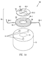
FIG. 1A shows an exploded view of a bimorph mirror assembly in accordance with an embodiment of the disclosure. -
FIG. 1B shows an assembled view of the bimorph mirror assembly ofFIG. 1A . -
FIG. 1C shows a side view of the bimorph mirror assembly ofFIG. 1B . -
FIG. 2 shows a method of assembling a bimorph mirror assembly in accordance with an embodiment of the disclosure. -
FIG. 3 shows an annular piezo-ceramic actuator in accordance with an embodiment of the disclosure. -
FIG. 4 shows a thin optical mirror in accordance with an embodiment of the disclosure. -
FIG. 5 shows a piezo actuator in a self-centering level fixture in accordance with an embodiment of the disclosure. -
FIG. 6 shows an adhesive locating fixture on a self-centering assembly fixture in accordance with an embodiment of the disclosure. -
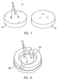
FIG. 7 shows a stand-off mold for forming stand-off mounts in accordance with an embodiment of the disclosure. -
FIG. 8 shows a clam-shell centering fixture for locating a bimorph mirror assembly on stand-offs in accordance with an embodiment of the disclosure. -
FIG. 9 shows a piezo actuator in a clam-shell centering fixture in accordance with an embodiment of the disclosure. -
FIG. 10 shows a mounted bimorph mirror assembly, in accordance with an embodiment of the disclosure. -
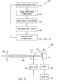
FIG. 11 shows a method of correcting a laser beam in accordance with an embodiment of the disclosure. -
FIG. 12 shows a laser system with a bimorph mirror assembly in accordance with an embodiment of the disclosure. -
FIGs. 13 A-C show various solid state laser systems with variable focus bimorph mirrors in accordance with the various embodiments of the disclosure. - Embodiments and their advantages are best understood by referring to the detailed description that follows. It should be appreciated that like reference numerals are used to identify like elements illustrated in one or more of the figures.
-
FIG. 1A is an exploded view of abimorph mirror assembly 100 in accordance with an embodiment of the disclosure.FIG. 1B is an assembled view of thebimorph mirror assembly 100 ofFIG. 1A .FIG. 1C is a side view of thebimorph mirror assembly 100 ofFIGs. 1A and1B . - Bimorph
mirror assembly 100 includes athin mirror 102 bonded to an annular thin piezoelectricceramic disk actuator 104. The bond formed to attachmirror 102 toactuator 104 may be beneficially formed to achieve uniform thickness in order to minimize flatness or curvature distortion ofmirror 102 under the action ofactuator 104. Since a first side ofmirror 102 may typically form one reflecting surface (e.g., a first surface) in the interior of a laser cavity,mirror 102 may be coated so the reflectivity of the first surface (i.e., the surface not bonded to actuator 104) may have a reflectivity between approximately 4% (i.e., the reflectivity of many uncoated optical glasses) to approximately 100%. For many laser applications it is preferred that the reflectivity of the first surface be approximately 99.99% or higher. A second side ofmirror 102 may or may not serve as an output coupling mirror. Therefore the reflectivity of the second side (e.g., a second surface) may be between approximately 4% and approximately 0%, where lower reflectivity may improve the quality of the output coupled beam. - Either or both sides of
mirror 102, and preferably the first surface may be ground and polished to a surface flatness of less than approximately 1/40th of a wave root-mean-square deviation in wave-front quality at the wavelength of operation. Maintaining this degree of flatness throughout the coating and assembly processes is preferable if higher order aberrations are to be avoided during fabrication. Standard wave-front testing may be performed using standard metrology wave-front interferometers, such as may be obtained from 4D Technology Corporation or Zygo Corporation. In one embodiment, the first and second surfaces ofmirror 102 may exhibit wave-front uniformity better than a selected wave-front criteria for light at a selected wavelength, as may be desired. -
Bimorph mirror assembly 100 is mounted to abase mount 110 using a plurality of flexible posts 112 (also referred to as stand-offs) having low stiffness. Acentral portion 103 ofmirror 102 having a diameter 102-1 is identified in which a central portion of a laser beam may partially transmit throughmirror 102. The diameter 102-1 ofcentral portion 103 is generally determined by inner diameter 104-2 ofactuator 104. The transmitted optical power of the laser beam may be absorbed bybase mount 110.Base mount 110 may be comprised of a material selected for a combination of properties, including heat capacity, thermal conductivity, and thermal coefficient of expansion. For example, in one embodiment,base mount 110 may be comprised of invar. -
Flexible posts 112 provide attachment of a bonded mirror-actuator subassembly 116 in a manner that substantially eliminates the transmission of stress betweenactuator 104 andbase 110.Flexible posts 112 may be made of a low outgassing material such as silicone rubber adhesive sealant (e.g., RTV™), molded in place to facilitate mounting of the mirror-actuator subassembly.Flexible posts 112 may provide mechanical isolation frombase 110 so that differences in thermal expansion do not transmit distorting stress to subassembly 116 resulting from heat absorbed inbase 110 from transmitted laser power. - An outer diameter 104-1 of
actuator 104 may be chosen to be larger than a mirror outer diameter 102-2, so that electrical connections to actuator 104 may be made. A pair of electrode wires 106-1 and 106-2 may be attached toactuator 104 atlocations 108. Wire 106-1 may be attached to the surface ofactuator 104 to whichmirror 102 is bonded, and wire 106-2 may be attached to the side ofactuator 104 that faces mountingbase 110. Attachment may be achieved with various bonding methods, including soldering. Attachment of wires 106 may be performed atlocations 108 onactuator 104 and in a manner to minimize distortion ofsubassembly 116 in order to produce a change in the curvature ofmirror 104 that is radially symmetric. - Prior to assembly and use,
actuator 104, as fabricated, may have hysteresis, i.e., when a periodic voltage is applied there is a phase lag between the applied voltage and the elastic deformation ofpiezoelectric actuator 104. Additionally, this is manifest in a non-return to the same initial dimension (i.e., zero strain) when the voltage is removed. The process ofmanufacturing actuator 104 may include a hot pressing and sintering of ceramic powder, followed by poling at elevated temperatures. This may induce internal stresses that are responsible for the hysteresis. A process of "training," wherebyactuator 104 is periodically stressed to a maximum strain value by application of a periodic bipolar voltage of a selected maximum amplitude and number of cycles may relax internal stresses by relieving internal dislocations. In an embodiment,actuator 104 comprises a polycrystalline material with considerable inter-atomic dislocation stress at the grain boundaries. -
Subassembly 116 includesactuator 104 bonded tomirror 102, which, in one embodiment, comprises standard grade fused silica (e.g., Corning 7980). The actuator is shown inFIG. 3 and the mirror is shown (separately) inFIG. 4 . In one embodiment, the dimension ofactuator 104 is 1.375" OD x 0.591" ID x .010" THK, and the dimension ofmirror 102 is 1.000"Ø x .028" THK. In this regard, it will be appreciated that an outer lateral dimension of actuator 104 (1.375" in this example) may be greater than an outer lateral dimension of mirror 102 (1.000" in this example) to provide space to attach electrical wire leads and maintain uniform strain onmirror 102. It is contemplated that different dimensions may be used in other embodiments. -
FIG. 2 shows a method of assembling abimorph mirror assembly 100 in accordance with an embodiment of the disclosure. The first assembly procedure includes soldering control leads to actuator 104 (block 210) using standard soldering techniques. Thin, highly compliant wires are preferred to avoid induced bending moments onactuator 104. A liquid solder flux may preferably be used. - The next set of assembly procedures may preferably be performed on a laminar flow-bench in a clean room, and standard glove and facial coverings may also preferably be used. In one embodiment,
actuator 104, the surfaces of mirror 102 (front and back) may be thoroughly cleaned and all residue (including solder flux) and particulates removed. Standard filtered compressed air to blow particulates, solvents (e.g., acetone, methanol, and isopropanol) and lint-free cloths to clean surfaces may be used in this regard.Actuator 104 may first be cleaned with acetone and lint-free cloth, followed by a second wiping with methanol and finally a wiping with isopropanol. The front surface ofmirror 102 may be placed face down on a lint-free cloth and a standard drag wipe with isopropanol and a laboratory grade lens tissue may be applied to clean the back side, which will be bonded toactuator 104. - A self-centering
level assembly fixture 500, as shown inFIG. 5 , may be used for the next assembly procedure. Using various steps as described above,fixture 500 may be pre-cleaned with compressed air and a wipe-down with isopropanol. A bubble level may be used to obtain proper leveling offixture 500 and to avoid any runs when later applying liquid adhesive.Actuator 104 may then be placed into fixture 500 (block 220), as shown inFIG. 5 . A self-centeringadhesive locating fixture 600 may be pre-cleaned, as above, and may be placed overactuator 104, as shown inFIG. 6 , and fastened in place, for example, with set screws (not shown). Locating holes (not shown) infixture 600 should be thoroughly flushed with acetone and isopropanol, using a syringe and blunt-tip hypodermic needle prior to use. - In
block 230,mirror 102 is bonded toactuator 104. In one embodiment, a self-centering vacuum chuck (not shown) to holdmirror 102 may be used inblock 230. The chuck may be pre-cleaned with acetone and isopropanol wipe-downs in preparation forbonding mirror 102 toactuator 104. - A mixture of a two part ultra-low viscosity surface epoxy adhesive may preferably be used in the bonding process. An epoxy with a room-temperature cure time in excess of 3 hours may be preferred, as a faster cure time may generally induce higher localized heating and exhibit greater shrinkage, both of which may distort
mirror 102 during the cure step. - In one exemplary embodiment, West Systems brand #105 resin with #209 extra-slow hardener, having a 3.5:1 mixture ratio, may be used for the bonding. It is preferred that weight measurements be as precise as feasible to avoid applying either too much or too little adhesive to the bond surface. Weights indicated below are exemplary, and have been found to be acceptable for the dimensions pertaining to subassembly 116 described above. For example, using a precision scale, 1.556 grams of West Systems #105 epoxy resin may be measured into an appropriate mixing container. The container may preferably be clean and comprised of a material with low particulate generation, impervious to the epoxy chemicals. One example of a container is a disposable aluminum mixing dish. 0.444 grams of West Systems #209 epoxy hardener may be weighed out and added to the resin, for a total mass of 2.000 g. 0.050 grams of 5 µm diameter silica micro-sphere filler material (precision glass beads) may then be added to ensure a uniform bond-line thickness of 5 µm. In other embodiments the bond-line thickness may range from approximately 10 nanometers and approximately 0.1 millimeter. It should be appreciated that the uniformity of the thickness is a factor in maintaining the wave-front properties of
mirror 102. - The components may be thoroughly mixed for 5 minutes, with a gentle mixing motion to ensure a minimal amount of entrapped air, and to maintain the glass beads in uniform suspension. Other commercially available epoxies may be used having various weights as may be desired depending on ambient conditions such as, for example, temperature, humidity, or atmospheric pressure, and by the details of the manufacturer's formulation. Preferably, the glass beads may maintain a substantially high uniformity of thickness of the adhesive bond-line provided the suspension is uniformly mixed when dispensed, and care should be taken to minimize entrapped air. Variations in quantities may occur for varying assembly conditions and applications (such as for example, a larger or
smaller subassembly 116, or different selection of bead size). - A syringe, with the orifice cap left on and the plunger removed, may be filled with the wet epoxy mixture. The plunger tip may be replaced, and the syringe inverted so that the mixture runs toward the plunger. The orifice cap may then be removed and a ½ inch - 25 gage needle installed, and the air may then be expelled from the syringe by carefully forcing the plunger upward. The needle may be placed into each locating hole (not shown) of
fixture 600 to apply exactly one drop of adhesive at each location as may typically be dispensed from a 25 gage needle. It will be appreciated that variations in the dimensions of various structures may result in more or less epoxy mixture being dispensed. In one embodiment, the viscosity of the epoxy may preferably be in the range from approximately 725 centipoise to approximately 1000 centipoise. It is contemplated that different viscosity ranges may be used in various embodiments depending on the sizes of glass beads or the dimensions ofmirror 102 andactuator 104. In one embodiment, set screws (not shown) may then be loosened and theadhesive locating fixture 600 removed fromassembly fixture 500. -
Mirror 102 may be placed on the above-identified vacuum chuck with the high reflectivity coated side face down, taking precaution to ensure thatmirror 102 may be centered on the chuck. The vacuum to the chuck may be enabled to holdmirror 102. The chuck may be carefully inverted over a clean lint-free cloth to test for proper vacuum seal. The chuck may then be placed over theassembly fixture 500, and care may be taken to ensure that it is properly seated. The vacuum may then be disabled, and several seconds allowed for the vacuum to release sufficiently formirror 102 to drop onto the adhesive preppedactuator 104. - The chuck may then be removed from
fixture 500, and thefixture 500 may then be left undisturbed for a minimum of 24 hours. The resultant bond-line is preferably very thin, and its uniformity and dimension is determined substantially by the size of the glass beads. Uniformity of the bond-line is intended to avoid distortion ofmirror 102 due to non-uniform shrinkage of the adhesive that may occur if the adhesive layer is too thick. -
Fixture 500 may then be cleaned of adhesive residue using acetone and a 22 gage needle to flush the holes, followed by a similar flushing with isopropanol. The surfaces may be wiped with acetone, then isopropanol, using a clean soft lint-free cloth. - The completed
subassembly 116 may be tested (for example, using standard wave-front testing as previously described herein) for wave front error after 24 hours of initial cure time. In one exemplary embodiment, it may be preferred that the flatness of mirror 102 (either the front or the back) be flat to approximately 1/40th of a wave at the wavelength of the laser. Other applications may be implemented with more or less stringent wave-front flatness. Immediately after each test,subassembly 116 may be returned toassembly fixture 500 to ensure a flat, level mating surface for the remainder of the cure. In one embodiment, actuation voltage is not to be applied toactuator 104 for a minimum of 2 weeks, to ensure the adhesive is fully cured before introducing any bending stress. - Subassembly 116 may preferably be supported on
base mount 110 with flexible posts 112 (i.e., stand-offs) to allow for proper alignment in an optical system. Additionally,flexible posts 112 may preferably be sufficiently compliant to allow for the bending deformation induced by the actuation voltage without significant mechanical coupling tobase mount 110, which may be comprised of a stiff material. In one embodiment,flexible posts 112 may be comprised of a space-grade silicone rubber compound such as, for example, part number RTV™ 566, manufactured by GE Bayer Silicones, which may yield good results due to its low stiffness and low out-gassing characteristics under high heat load. Becausemirror 102 may be used in a high-energy laser resonator, any energy that leaks through the mirror coating will be nearly entirely absorbed inbase mount 110. In one embodiment, invar 36 may be used forbase 110, due to its low coefficient of thermal expansion (CTE). - Referring to
FIG. 7 , a Teflon™ stand-offmold 701 may be placed overbase mount 110 to form flexible posts 112 (block 240). An appropriate quantity of compliant, low out-gassing RTV™ compound may be mixed and injected into themold 701 using, for example, a 14 gage stainless steel needle and syringe, and allowed to cure. After curing, a razor blade or knife may be used to cut away the spill-over material, so that eachflexible post 112 is flat and flush with the top ofmold 701. After curing,mold 701 may be lifted from the substrate without any twisting motion to avoid shearing the stand-offs. - During
block 260 ofFIG. 2 , clam-shell bimorph mirror alignment fixture 800 (seeFIG. 8 ) may be placed overbase mount 110 and secured with a rubber band. RTV™ compound may be mixed and dabbed onto the cured ends of eachflexible post 112. Subassembly 116 may be placed infixture 800 to adhere subassembly 116 to flexible posts 112 (block 260) as shown inFIG. 9 .Mirror 102 may be covered with a piece of lens tissue folded several times to protect the surface. A small weight of approximately one to two ounces may be applied for several seconds to forcesubassembly 116 ontoflexible posts 112, spreading the uncured RTV™ compound to adhere subassembly 116 toflexible posts 112. The weight may be removed and thebimorph mirror assembly 100 may be allowed to cure. Stand-offposts 112 may be fabricated from other flexible curable materials than RTV™, which is an exemplary material. -
FIG. 10 shows a complete mountedbimorph mirror assembly 100, in accordance with an embodiment of the disclosure. Multiple sensor leads 1002 (e.g., implemented by multiple strands of 36 gage wire) may be attached (block 270) to, for example, four radially located strain gages (optional, not shown) attached to the back of the device. Wires 106-1 and 106-2 are also (previously) attached. After final assembly, the device may be packaged and wires 106-1, 106-2 and sensor leads 1002 may terminated appropriately for integration into an optical system. - As an example,
FIG. 11 illustrates amethod 1100 of correcting a laser beam. A portion of the laser beam pattern is received by a beam pattern intensity sensor (block 1110). As an example, a beam splitter may be used to direct a small fraction of the beam to the sensor. The beam splitter may be external to the laser or, alternatively, it may be intra-cavity. The beam pattern and intensity may be segmented or digitized into pixels. Other known methods of beam sensing may be substituted accordingly. - The received intensity pattern is compared to a desired beam intensity pattern (block 1120). In
block 1130, a controller may generate voltage commands to an amplifier based on the comparison ofblock 1120. For example, a differential mapping of the actual versus the desired beam pattern may be generated by the controller. The magnitude of the intensity differences in pixels of corresponding desired and actual pattern intensity distribution may be used to generate voltage vector value commands (i.e., polarity and amplitude). - The voltage commands (which may be, for example, in digital format) may be converted to amplified analog voltages by a digital-to-analog amplifier, which are then applied to the wires 106 attached to actuator 104 (block 1140). The applied voltages may cause actuator 104 to deform
mirror 102 to correct the beam pattern (block 1150). Strain gages may be attached toactuator 104 to measure strain, a beam pattern sensor may characterize the beam, and the two sets of sensor signals may be correlated to control the actuator for desired beam characteristics. The process may be iterative, so that the method may continue by returning to block 1110 for continuously receiving beam intensity patterns for beam correction until, for example, a received beam intensity pattern substantially corresponds to the desired beam pattern. - An implementation of
assembly 100 in alaser system 1200 is shown inFIG. 12 . Alaser 1210 may contain one or more solid state laser rods or slabs of lasing material, which may be excited by, for example, optical pumping (not shown) of light of suitable intensity and wavelength. A resonant cavity is formed by containing thelaser 1210 between two high reflectance mirrors, one of which may beoutput mirror 1220, and the other may bemirror 102 ofbimorph mirror assembly 100. In the case of cylindrical rod laser material, temperature and stress-induced changes in the refractive index of the lasing material may be radial in nature due to the rod symmetry. The refractive index gradient induced radially may result in self-focusing types of effects, and alter the distribution of intensity and phase in the beam in a like manner. Altering the curvature ofmirror 102 may compensate for this effect. By applying a voltage toactuator 104, a dimensional change may be produced in the radial direction ofactuator 104. The bondedmirror 102, however, may constrain the surface stress condition on the bonded side ofactuator 104, which is different from that of the opposite side ofactuator 104. This may result in a change in the curvature ofmirror 102. Depending on the applied voltage, the curvature ofmirror 102 may be concave or convex. This change may enable a more uniform distribution of energy and laser excitation in the lasing material and beam aperture oflaser 1210. - A fraction of the beam produced in the cavity of
laser system 1200 may be split off by aprism cube 1230, or equivalent, and directed from the cavity oflaser system 1200 to abeam characterization sensor 1240. Examples of beam characterization sensors include wave-front sensors and intensity pattern sensors. The beam distribution obtained may be used in a controller 1250 (also referred to as a control filter) to generate a one or more commands to a voltage generator 1260 (also referred to as an amplifier, or voltage amplifier) to apply a corrective voltage to the one or more segments ofactuator 104 to adjust the beam distribution detected insensor 1240.Beam characterization sensor 1240 may generate sensor information in digital or analog form.Controller 1250 may generate commands in analog or digital form. Ifsensor 1240 andcontroller 1250 output have a digital form, for example,voltage generator 1260 may perform a digital-to-analog (D/A) conversion to provide an amplified analog voltage to segments ofactuator 104. For the exemplary dimensions ofsubassembly 116 as described above, implementation in an appropriately dimensioned laser cavity may have an actuation response bandwidth from 0 Hz to approximately 1000 Hz. This bandwidth may have a higher or lower upper limit, depending on the mechanical properties ofsubassembly 116 and the stability properties of the laser. A specific laser design, mechanical dimensions, and materials stiffness (e.g., foractuator 104 and mirror 102) may determine the operational parameters for speed of response ofsensor 1240,controller 1250, and generator 160. - In another embodiment in accordance with the disclosure,
actuator 104 may have segmented electrodes to selectively apply voltages of different values circumferentially aboutactuator 104. This may employ a larger number of electrodes, and the applied voltages may be bipolar, so that some portions ofsubassembly 116 act to change the curvature ofmirror 102 in a convex manner in some locations and concave in others. In this manner, it may enable subassembly 116 to correct higher order beam distortions. Strain gages (not shown) may be attached to subassembly, preferably on the rear surface ofactuator 104, to measure strain to correlate with signals at least fromgenerator 1260 andsensor 1240. -
FIGs. 13 A-C illustrates various embodiments of a solid state laser system with a variable focus bimorph mirror in accordance with the disclosure. - Referring to
FIG. 13A , alaser cavity 1301 includes anoutput mirror 1320, a solid state laser gain medium comprised of one or more solidstate laser rods 1310, and mirror-actuator subassembly 116. In this embodiment,mirror 102 ofsub-assembly 116 may be a primary high reflecting mirror in a stable or unstable resonator configuration. The associated control system ofFIG. 12 , comprisingbeam splitter 1230,sensor 1240,controller 1250 and voltage generator 1160 are not shown, but may be implemented by way of reference toFIG. 12 . - Referring to
FIG. 13B ,mirror 102 ofsubassembly 116 may be partially transmitting and serve as an output mirror in a stable or unstable resonator. In this case, base mount 110 (not shown), on whichsubassembly 116 is mounted, may additionally be provided with an annulus through hole (not shown) to accommodate the output beam. Amirror 1325 may serve as a high reflectivity mirror forming one end of the resonator cavity. As inFIG. 13A , the associated control system is not shown, but may be implemented by way of reference toFIG. 12 . - Referring to
FIG. 13C ,mirror 102 ofsubassembly 116 may be used as a high reflectance folding mirror in a stable or unstable resonator cavity that includes a nonlinearoptical element 1330. Amirror 1325 may serve as a high reflectivity mirror forming one end of the resonator cavity, andmirror 1320 may form the other cavity mirror, having partial transmission to serve as an output for the laser beam. Nonlinearoptical element 1330 may provide one or more nonlinear optical functions, such as, for example, frequency doubling, Raman shifting, or frequency mixing. In this case the reflectivity of all mirrors inFIG. 13C , includingmirror 102, may take into account reflectivity at more than one frequency. - In this embodiment, since a portion of the beam incident on
mirror 102 may be transmitted through tobase mount 110 at a non-normal angle of incidence, laser energy may be absorbed by this structure in a non-symmetric manner. This may result in a non-uniform heating ofbase mount 110, which in turn may cause a non symmetric heating offlexible posts 112. Thus, the thermal load may be different for eachflexible post 112. Since materials such as may be used forflexible posts 112 may typically have higher coefficients of thermal expansion (CTE) than thebase mount 110 material (e.g., invar), thermally induced pointing error ofmirror 102 may result, which may be measured and corrected. - In this case, a
base mount 110A may incorporate a motor actuated tip-tilt stage capable of goniometric rotation θ, ϕ about two perpendicular axes. Correction pointing may be implemented, for example, by monitoring the beam with beam sensor 1240 (FIG. 12 ) or an equivalent, and a correction filter (e.g., which may be incorporated incontrol filter 1250 or separately) may generate feedback control commands to drive the tip-tilt axes ofbase mount 110A to correct pointing error. A diagnostic laser beam, such as provided by a diode laser (not shown) may be injected into the laser cavity (e.g., throughprism 1230 ofFIG. 12 , or an equivalent prism placed appropriately) and the diagnostic beam reflected frommirror 102 may be monitored in a manner similar or equivalent to that described above pertaining to beam characterization. - Embodiments described above illustrate but do not limit the disclosure. It should also be understood that numerous modifications and variations are possible in accordance with the principles of the present disclosure. Accordingly, the scope of the disclosure is defined only by the following claims.
Claims (18)
- A laser beam correction system comprising:a mirror (102) having a first surface and a second surface;an actuator comprising a piezoelectric ceramic disk (104) and a plurality of conductive electrodes (106) on substantially opposing sides of the disk (104), wherein the actuator (104) is bonded to the second surface of the mirror (102), and wherein the actuator (104) comprises an aperture substantially in a center portion of the disk; anda wave-front sensor adapted to measure optical wave-front characteristics of a laser beam received by the mirror (102) and provide electronic signals corresponding to the wave-front characteristics.
- The system of claim 1, further comprising a control filter (1250) adapted to convert the electronic signals to actuator (104) commands.
- The system of claim 2, further comprising an amplifier (1260) adapted to convert the commands to voltages to be applied to the electrodes of the actuator (104) to correct the optical wave-front of the laser beam, wherein the amplifier (1260) is adapted to accept analog and/or digital commands from the control filter (1250) and output analog voltages to the actuator (104).
- The system of claim 3, wherein the actuator (104), the control filter (1250), and the amplifier (1260) have an actuation response bandwidth of 0 Hz to approximately 1000 Hz.
- The system of claim 1, wherein the actuator (104) comprises a plurality of segments adapted to control focus and higher order optical aberrations, wherein each segment comprises a pair of electrodes (106) on substantially opposing sides of the actuator (104).
- The system of claim 1 further comprising a base mount (110) facing the actuator (104) and the second surface of the mirror (102), wherein the mounting base (110) supports the mirror (102) and actuator (104).
- The system of claim 6, further comprising:wherein the base mount (110) comprises a motor actuated tip-tilt stage adapted to support the mirror (102) and the actuator (104);a pointing sensor (1240) adapted to measure alignment of a beam reflected from the first surface of the mirror (102) and provide electronic signals corresponding to the error of the measured pointing directions of the mirror (102); anda correction filter adapted to receive the electronic signals corresponding to the pointing direction errors and generate actuator commands to the tip-tilt stage to correct the orientation of the mirror (102), wherein the alignment beam is provided by a diagnostic beam introduced into the laser cavity, and wherein the pointing sensor (1240) is implemented by the optical wave-front sensor.
- The system of claim 7, further comprising a beam splitter adapted to direct a portion of the laser beam to one of the pointing sensor (1240) or the wave-front sensor.
- The system of claim 1, wherein the mirror (102) and actuator (104) comprise a bimorph correction mirror assembly (100), the assembly is adapted to correct a thermally induced wave-front error of the laser beam.
- The system of claim 1, wherein the first surface is coated with a first reflectivity coating and the second surface is coated with a second reflectivity coating at one or more selected wavelengths, wherein the first reflectivity coating has a reflectivity between approximately 4% and approximately 100%, and wherein the second reflectivity coating has a reflectivity less than approximately 4%.
- A method of manufacturing a bimorph wave-front correction mirror, the method comprising:providing a mirror (102) having a first surface and a second surface, wherein the first and second surfaces exhibit wave-front uniformity better than a selected wave-front criteria for light at a selected wavelength;forming a poled annular piezoelectric ceramic disk (104), wherein the disk (104) has a first side and a second side, an aperture substantially in a center portion of the disk (104), one or more pairs of electrodes (106) on substantially opposing sides of the disk (104), and an outer lateral dimension greater than an outer lateral dimension of the mirror (102);stress cycling the disk (104) by applying a periodic bipolar voltage to the electrode pairs (106);bonding the second surface of the mirror (102) to the first side of the disk (104) with adhesive to achieve a substantially zero stress bond to maintain the wave-front quality of the mirror (102) after assembly of the mirror/disk (102/104) combination;connecting wires to substantially opposing conductive electrode (106) pairs on the disk (104) adapted to apply a voltage to enable piezoelectrically induced strain to deform the bonded mirror (102) by a selected amount; andmounting the second side of the disk (104) to a mounting base (110) using a plurality of stand-offs (112) adapted to adhere the disk (104) to the mounting base (110).
- The method of claim 11, wherein the mounting base (110) comprises an aperture substantially in a center portion of the mounting base (110), wherein the aperture of the mounting base (110) is greater than the aperture of the disk (104).
- The method of claim 11, further comprising attaching one or more strain sensors to the disk (104).
- The method of claim 11, wherein the providing comprises:polishing the mirror (102) on both a first surface and a second surface to exhibit less than approximately 1/40th of a wave root-mean-square deviation in wave-front surface quality at a specified wavelength;coating the first surface of the mirror (102) with a first reflectivity coating to achieve a specified reflectivity at a first specified wavelength over at least a first specified portion of the mirror (102); andcoating the second surface of the mirror (102) with a second reflectivity coating to reduce reflection at a second specified wavelength below a second specified amount over at least a second specified portion of the mirror (102).
- The method of claim 14, wherein the first reflectivity coating has a reflectivity between approximately 4% and approximately 100%, and wherein the second reflectivity coating has a reflectivity less than approximately 4%.
- The method of claim 11, wherein the bonding comprises:statically leveling the disk (104);cleaning the first side of the disk (104) and the second surface of the mirror (102);applying an epoxy to an interface between the mirror (102) and the disk (104); andcuring the epoxy in a statically undisturbed state at a controlled temperature.
- The method of claim 16, wherein the epoxy has a viscosity between approximately 725 and approximately 1000 centipoise, and wherein the thickness of the epoxy layer is between approximately 10 nanometers and approximately 0.1 millimeter.
- The method of claim 16, wherein the curing is performed for longer than 24 hours.
Applications Claiming Priority (1)
| Application Number | Priority Date | Filing Date | Title |
|---|---|---|---|
| US11/760,562 US7473878B2 (en) | 2007-06-08 | 2007-06-08 | High power bimorph wave-front correction mirror |
Publications (2)
| Publication Number | Publication Date |
|---|---|
| EP2009480A2 true EP2009480A2 (en) | 2008-12-31 |
| EP2009480A3 EP2009480A3 (en) | 2010-03-10 |
Family
ID=39970851
Family Applications (1)
| Application Number | Title | Priority Date | Filing Date |
|---|---|---|---|
| EP08251940A Withdrawn EP2009480A3 (en) | 2007-06-08 | 2008-06-04 | High power bimorph wave-front correction mirror |
Country Status (3)
| Country | Link |
|---|---|
| US (1) | US7473878B2 (en) |
| EP (1) | EP2009480A3 (en) |
| JP (1) | JP5308074B2 (en) |
Families Citing this family (3)
| Publication number | Priority date | Publication date | Assignee | Title |
|---|---|---|---|---|
| US9285516B2 (en) | 2010-08-02 | 2016-03-15 | Avinash Girish Bhardwaj | Actuator motion control mechanism for a concave mirror |
| WO2019206637A1 (en) | 2018-04-24 | 2019-10-31 | Asml Netherlands B.V. | Reflective optical element for a radiation beam |
| US20210036489A1 (en) * | 2019-08-02 | 2021-02-04 | Innolight Technology (Suzhou) Ltd. | Narrow linewidth external cavity laser and optical module |
Citations (3)
| Publication number | Priority date | Publication date | Assignee | Title |
|---|---|---|---|---|
| GB2128733A (en) * | 1982-10-14 | 1984-05-02 | Messerschmitt Boelkow Blohm | An adaptive optical system |
| JP2004333943A (en) | 2003-05-08 | 2004-11-25 | Olympus Corp | Mirror with variable shape and optical device using mirror with variable shape |
| WO2006098403A1 (en) * | 2005-03-17 | 2006-09-21 | Brother Kogyo Kabushiki Kaisha | Light reflecting element, light reflecting device, wave front curvature modulator, and optical scanning type display device |
Family Cites Families (18)
| Publication number | Priority date | Publication date | Assignee | Title |
|---|---|---|---|---|
| US3731103A (en) * | 1971-02-24 | 1973-05-01 | Hughes Aircraft Co | Adaptive arrays |
| US4438330A (en) * | 1982-03-01 | 1984-03-20 | Itek Corporation | Wavefront sensor employing a modulation reticle |
| US5026977A (en) * | 1989-04-05 | 1991-06-25 | The Charles Stark Draper Laboratory, Inc. | Wavefront sensing and correction with deformable mirror |
| US5016997A (en) * | 1990-05-15 | 1991-05-21 | The United States Of America As Represented By The United States Department Of Energy | Partially segmented deformable mirror |
| JP2893862B2 (en) * | 1990-05-16 | 1999-05-24 | ソニー株式会社 | Solid state laser oscillator |
| US5121405A (en) * | 1990-12-20 | 1992-06-09 | Coherent, Inc. | Alignment control system for lasers |
| US6192064B1 (en) * | 1997-07-01 | 2001-02-20 | Cymer, Inc. | Narrow band laser with fine wavelength control |
| JP3219072B2 (en) * | 1999-02-17 | 2001-10-15 | 住友電気工業株式会社 | Variable shape mirror for laser beam |
| US6464364B2 (en) * | 2000-01-27 | 2002-10-15 | Aoptix Technologies, Inc. | Deformable curvature mirror |
| US6874897B2 (en) * | 2000-01-27 | 2005-04-05 | Aoptix Technologies, Inc. | Deformable curvature mirror with unipolar-wiring |
| US6452145B1 (en) * | 2000-01-27 | 2002-09-17 | Aoptix Technologies, Inc. | Method and apparatus for wavefront sensing |
| US6800988B1 (en) * | 2000-07-11 | 2004-10-05 | Technion Research & Development Foundation Ltd. | Voltage and light induced strains in porous crystalline materials and uses thereof |
| WO2004057407A1 (en) * | 2002-12-23 | 2004-07-08 | Bae Systems Plc | Deformable mirror |
| EP1576407A2 (en) * | 2002-12-23 | 2005-09-21 | BAE Systems PLC | Deformable-mirror cooling |
| EP1676163A2 (en) * | 2003-10-20 | 2006-07-05 | BAE Systems PLC | Improvements relating to deformable mirror holders |
| US7229178B1 (en) * | 2004-12-20 | 2007-06-12 | Sandia Corporation | Variable focal length deformable mirror |
| JP2007025503A (en) * | 2005-07-20 | 2007-02-01 | Topcon Corp | Deformable mirror deformation method, optical device using the method, and fundus oculi observation device |
| GB0526609D0 (en) | 2005-12-30 | 2006-02-08 | Imp College Innovations Ltd | A wavefront variation device |
-
2007
- 2007-06-08 US US11/760,562 patent/US7473878B2/en not_active Expired - Fee Related
-
2008
- 2008-06-04 EP EP08251940A patent/EP2009480A3/en not_active Withdrawn
- 2008-06-05 JP JP2008148165A patent/JP5308074B2/en not_active Expired - Fee Related
Patent Citations (3)
| Publication number | Priority date | Publication date | Assignee | Title |
|---|---|---|---|---|
| GB2128733A (en) * | 1982-10-14 | 1984-05-02 | Messerschmitt Boelkow Blohm | An adaptive optical system |
| JP2004333943A (en) | 2003-05-08 | 2004-11-25 | Olympus Corp | Mirror with variable shape and optical device using mirror with variable shape |
| WO2006098403A1 (en) * | 2005-03-17 | 2006-09-21 | Brother Kogyo Kabushiki Kaisha | Light reflecting element, light reflecting device, wave front curvature modulator, and optical scanning type display device |
Non-Patent Citations (2)
| Title |
|---|
| LEE ET AL.: "A circular bimorph deformable mirror for circular/annulus/square laser beam compensation", JOURNAL OF THE OPTICAL SOCIETY OF KOREA, vol. 10, no. 1, 1 March 2006 (2006-03-01), pages 23 - 27, XP009128224, DOI: doi:10.3807/JOSK.2006.10.1.023 |
| LEE J H ET AL: "A circular bimorph deformable mirror for circular/annulus/square laser beam compensation", JOURNAL OF THE OPTICAL SOCIETY OF KOREA, OPTICAL SOCIETY OF KOREA, SEOUL, KR, vol. 10, no. 1, 1 March 2006 (2006-03-01), pages 23 - 27, XP009128224, ISSN: 1226-4776, DOI: 10.3807/JOSK.2006.10.1.023 * |
Also Published As
| Publication number | Publication date |
|---|---|
| JP2008304918A (en) | 2008-12-18 |
| US7473878B2 (en) | 2009-01-06 |
| US20080302948A1 (en) | 2008-12-11 |
| JP5308074B2 (en) | 2013-10-09 |
| EP2009480A3 (en) | 2010-03-10 |
Similar Documents
| Publication | Publication Date | Title |
|---|---|---|
| TWI691746B (en) | Integrated optical assembly, optical communication system and method for manufacturing integrated optical assembly | |
| US7173713B2 (en) | Optical fiber sensors for harsh environments | |
| CN102576149B (en) | For the actuator of mobile micro mechanical organ | |
| JP3955438B2 (en) | Curved optical device and manufacturing method thereof | |
| US20100202071A1 (en) | Deformable mirror | |
| US20070013914A1 (en) | Crystalline optical fiber sensors for harsh environments | |
| US8432661B2 (en) | Microstructural body and production method therefor | |
| CN115061114A (en) | Laser radar transmitting system, scanning method and wafer-level packaged device | |
| JP2005505000A (en) | Beam steering optical switching element | |
| EP2856241B1 (en) | Modal corrector mirror with compliant actuation for optical aberrations | |
| WO2009134407A1 (en) | Optical package having deformable mirrors for focus compensation | |
| US7473878B2 (en) | High power bimorph wave-front correction mirror | |
| RU2623661C2 (en) | Method of compensation of optical aberrations using a deformed mirror | |
| CN115480358B (en) | Deformable mirror driven by ultrasonic resonance | |
| Verpoort et al. | Characterization of a miniaturized unimorph deformable mirror for high power cw-solid state lasers | |
| US6953254B2 (en) | Silicon wafer based macroscopic mirror for wide angle scanning applications | |
| CN118393677B (en) | A high-frequency stacked deformable mirror and its assembly method | |
| WO2010127060A1 (en) | Folded lasers system | |
| Leitz et al. | Vibration and shock testing of a 50 mm aperture unimorph deformable mirror | |
| Helmbrecht et al. | Segmented MEMS deformable-mirror for wavefront correction | |
| TWI853543B (en) | Temperature-insensitive actuator and deformation mirror | |
| Helmbrecht et al. | Segmented MEMS deformable-mirror technology for space applications | |
| US12055788B2 (en) | Thermally actuated adaptive optics | |
| Neufeld et al. | The active primary mirror assembly for the SOAR telescope | |
| JP2008304918A5 (en) |
Legal Events
| Date | Code | Title | Description |
|---|---|---|---|
| PUAI | Public reference made under article 153(3) epc to a published international application that has entered the european phase |
Free format text: ORIGINAL CODE: 0009012 |
|
| 17P | Request for examination filed |
Effective date: 20080604 |
|
| AK | Designated contracting states |
Kind code of ref document: A2 Designated state(s): AT BE BG CH CY CZ DE DK EE ES FI FR GB GR HR HU IE IS IT LI LT LU LV MC MT NL NO PL PT RO SE SI SK TR |
|
| AX | Request for extension of the european patent |
Extension state: AL BA MK RS |
|
| PUAL | Search report despatched |
Free format text: ORIGINAL CODE: 0009013 |
|
| AK | Designated contracting states |
Kind code of ref document: A3 Designated state(s): AT BE BG CH CY CZ DE DK EE ES FI FR GB GR HR HU IE IS IT LI LT LU LV MC MT NL NO PL PT RO SE SI SK TR |
|
| AX | Request for extension of the european patent |
Extension state: AL BA MK RS |
|
| 17Q | First examination report despatched |
Effective date: 20101006 |
|
| AKX | Designation fees paid |
Designated state(s): AT BE BG CH CY CZ DE DK EE ES FI FR GB GR HR HU IE IS IT LI LT LU LV MC MT NL NO PL PT RO SE SI SK TR |
|
| STAA | Information on the status of an ep patent application or granted ep patent |
Free format text: STATUS: THE APPLICATION IS DEEMED TO BE WITHDRAWN |
|
| 18D | Application deemed to be withdrawn |
Effective date: 20181127 |