EP2006956A2 - System and method for a radio frequency (RF) transition design for a phased array antenna system utilizing a beam forming network - Google Patents
System and method for a radio frequency (RF) transition design for a phased array antenna system utilizing a beam forming network Download PDFInfo
- Publication number
- EP2006956A2 EP2006956A2 EP08252104A EP08252104A EP2006956A2 EP 2006956 A2 EP2006956 A2 EP 2006956A2 EP 08252104 A EP08252104 A EP 08252104A EP 08252104 A EP08252104 A EP 08252104A EP 2006956 A2 EP2006956 A2 EP 2006956A2
- Authority
- EP
- European Patent Office
- Prior art keywords
- wiring board
- printed wiring
- beam forming
- phased array
- transition
- Prior art date
- Legal status (The legal status is an assumption and is not a legal conclusion. Google has not performed a legal analysis and makes no representation as to the accuracy of the status listed.)
- Granted
Links
Images




Classifications
-
- H—ELECTRICITY
- H01—ELECTRIC ELEMENTS
- H01Q—ANTENNAS, i.e. RADIO AERIALS
- H01Q21/00—Antenna arrays or systems
- H01Q21/0006—Particular feeding systems
- H01Q21/0025—Modular arrays
-
- H—ELECTRICITY
- H01—ELECTRIC ELEMENTS
- H01P—WAVEGUIDES; RESONATORS, LINES, OR OTHER DEVICES OF THE WAVEGUIDE TYPE
- H01P5/00—Coupling devices of the waveguide type
- H01P5/08—Coupling devices of the waveguide type for linking dissimilar lines or devices
- H01P5/085—Coaxial-line/strip-line transitions
-
- H—ELECTRICITY
- H01—ELECTRIC ELEMENTS
- H01P—WAVEGUIDES; RESONATORS, LINES, OR OTHER DEVICES OF THE WAVEGUIDE TYPE
- H01P5/00—Coupling devices of the waveguide type
- H01P5/08—Coupling devices of the waveguide type for linking dissimilar lines or devices
- H01P5/10—Coupling devices of the waveguide type for linking dissimilar lines or devices for coupling balanced lines or devices with unbalanced lines or devices
- H01P5/107—Hollow-waveguide/strip-line transitions
-
- H—ELECTRICITY
- H01—ELECTRIC ELEMENTS
- H01Q—ANTENNAS, i.e. RADIO AERIALS
- H01Q21/00—Antenna arrays or systems
- H01Q21/0006—Particular feeding systems
- H01Q21/0075—Stripline fed arrays
-
- H—ELECTRICITY
- H01—ELECTRIC ELEMENTS
- H01Q—ANTENNAS, i.e. RADIO AERIALS
- H01Q21/00—Antenna arrays or systems
- H01Q21/0087—Apparatus or processes specially adapted for manufacturing antenna arrays
-
- H—ELECTRICITY
- H01—ELECTRIC ELEMENTS
- H01Q—ANTENNAS, i.e. RADIO AERIALS
- H01Q21/00—Antenna arrays or systems
- H01Q21/06—Arrays of individually energised antenna units similarly polarised and spaced apart
- H01Q21/061—Two dimensional planar arrays
- H01Q21/064—Two dimensional planar arrays using horn or slot aerials
Definitions
- the present disclosure relates generally to beam forming networks and more particularly to phased array antennas utilizing such networks.
- Active phased array antenna systems are capable of forming one or more antenna beams of electromagnetic energy and electronically steering the beams to targets, with no mechanical moving parts involved.
- a phased array antenna system has many advantages over other types of mechanical antennas, such as dishes, in terms of beam steering agility and speed, low profiles, low observability, and low maintenance.
- a beam forming network is a major and critical part of a phased array antenna system.
- the beam forming network is responsible for collecting all the electromagnetic signals from the array antenna modules and combining them in a phase coherent way for the optimum antenna performance.
- the element spacing in a phased array is typically at one-half of the wavelength for electromagnetic waves in space.
- phased array there are design challenges when utilizing a phased array antenna system. Firstly, it is important that the phased array include a rhombic shape of aperture for low observabilty requirements of the system. In addition, the system should be as small as possible to conserve space while still having the same performance characteristics of conventional shaped phased array antenna systems. Furthermore, as array antenna frequency increases, the element spacing decreases in an inversely proportional manner. Due to this tight spacing in phased arrays at microwave frequencies, transitions of radio frequency (RF) energy from inside of the beam forming network printed wiring board to the backside of the antenna have always been one of the critical RF design factors in phased array development. Conventional designs had tighter tolerances in the feature alignments of the RF transition, which limits the choice of suppliers for the systems and impacts the cost and schedule for producing the antennas as well.
- RF radio frequency
- a phased array antenna system includes a printed wiring board formed in rhombic shape that accommodates requirements for low observability, a beam forming network located within the printed wiring board, wherein the beam forming network is located over substantially the entire printed wiring board, and a plurality of connectors located on the backside of the printed wiring board configured to allow for expansion of the system.
- a method for forming a phased array beam includes providing a printed wiring board formed in a rhombic shape, providing a beam forming network located within the printed wiring board, wherein the beam-forming network is located over substantially the entire printed wiring board, and providing a plurality of connectors only on the back side of the printed wiring board to allow for expansion of the phased array beams.
- a radio frequency "RF" transition system includes a stripline trace section with openings in ground planes and forms a quarter wavelength resonator, and an electromagnetic mechanism to couple the RF energy from the stripline trace section to a connector, wherein the RF signal energy is transferred from inside a beam forming network printed wiring board to an antenna back plane with minimal RF losses.
- a radio-frequency "RF" transition module includes a first port, a can coupled above the first port, the can including dielectric material therein; wherein the can tunes the transition module by varying the properties of the dielectric material, a connector coupled to the first port, and a second port coupled to the connector, wherein the transition modules provide RF signals to a phased array antenna system.
- a phased array antenna system includes a printed wiring board formed in rhombic shape that accommodates requirements for low observability, a beam forming network located within the printed wiring board, wherein the beam forming network is located over substantially the entire printed wiring board, a radio-frequency "RF" transition system comprising a stripline trace section with openings in ground planes and forms a quarter wavelength resonator; and an electromagnetic mechanism to couple the RF energy from the stripline trace section to a connector, wherein the RF signal energy is transferred from inside the printed wiring board to an antenna back plane with minimal RF losses, and a plurality of connectors located on the backside of the printed wiring board that allows for expansion of the system.
- RF radio-frequency
- a method for transferring radio-frequency "RF" signal energy includes forming a quarter-wavelength resonator, and coupling the RF signal energy from a stripline trace section to a connector, wherein the RF signal energy is transferred from inside a beam forming network printed wiring board to an antenna back plane with minimal RF losses.
- the present embodiment relates generally to beam forming networks and more particularly to phased array antennas utilizing such networks.
- the following description is presented to enable one of ordinary skill in the art to make and use the embodiment and is provided in the context of a patent application and its requirements.
- Various modifications to the embodiments and the generic principles and features described herein will be readily apparent to those skilled in the art.
- the present embodiment is not intended to be limited to the embodiments shown, but is to be accorded the widest scope consistent with the principles and features described herein.
- Every phased array antenna system includes a beam forming network to coherently combine the signals from all of its many elements. It is this signal combining ability that forms the electromagnetic beam.
- a beam forming distribution board for a conventional phased array antenna system has a rectangular shape for the beam forming network. As is known the rectangular shape provides problems because it is easily observable electronically due to its electronic signature. Hence it is desirable for the phased array antenna system to be rhombic in shape to allow for low observability.
- phased arrays have been produced that contain a large number of phased array elements.
- the Boeing Company has produced such a phased array antenna system that contains 4,096 elements in 8 subarrays arranged in a 2x4 configuration.
- phased array antenna systems such as K-band arrays
- the rhombic shape of aperture for phased array antennas were accomplished by either using the metal plate itself, (which offered only the minimum benefit to the low observability), or having passive dummy elements placed around the rectangular shape of active elements.
- a phased array antenna system in accordance with an embodiment expands the capabilities of phased array antenna systems in two critical areas: (1) providing a low observability compliant phased array aperture with reduced size, weight and cost; and (2) providing a beam forming network scalability to large full- size arrays. Both capabilities allow for the enhanced phased array antennas utilized for a variety of applications. To describe the features of the phased array antenna system refer now to the following description in conjunction with the accompanying figures.
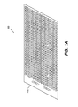
- FIG. 1A is a mechanical schematic of one embodiment of a beam forming network 100 within a printed wiring board 102.
- the beam forming network 100 is formed inside a rhombic shape printed wiring board (PWB) 102, so that two or more of such identical boards can be put together to form a larger sized array without compromising the low observability characteristics.
- PWB printed wiring board
- the rhombic shape of the aperture is covered with active beam forming elements for a maximum cost effective benefit to the antenna system.
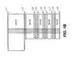
- the PWB 102 includes nine layers as shown in Figure 1B .
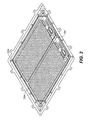
- FIG. 2 is a mechanical schematic of the receive phased array antenna system 200 with two subarrays 202a and 202b of the beam forming network, according to an embodiment.
- One critical feature is the narrowing of the non-active-element gaps around each board when two or more identical PWBs are put together to form large arrays.
- FIG. 2 shows that the edge gaps 204 in-between the adjacent boards are of only one element spacing, as compared with two element spacing in the conventional phased arrays. This reduction in the gap width improves the antenna beam patterns.
- the reduction of gap width is accomplished by laying out the beam forming circuits of the subarrays 202a and 202b in a more efficient manner. Also, by placing all of the circuitry and connectors on the backside adjacent subarrays, the subarrays can be placed closer together than the subarrays utilized in a conventional phased array antenna system.
- FIG. 3A is a diagram of a portion of the beam forming network circuits 200 inside the PWB 202.
- FIG. 3A shows stripline traces 302 on the RF layer 300 embedded inside the printed wiring board 202. These stripline traces 302 form the RF distribution network for the beam forming function.
- the data and clock lines are arranged in an orthogonal style to provide a more efficient layout on the PWB 202 and more robust signal integrity for array's beam steering control.
- FIG. 4 is a diagram of a receive phased array antenna assembly 400.
- one subarray 410a is shown assembled and one subarray 410b is shown in exploded view.
- the subarray 410b includes a plurality of subarray elements 412, a module shim 414, a multilayer wiring board (MLWB) 416, an elastomer connector shim 418 and a pressure plate with thermal transfer material 420.
- the MWLB is utilized advantageously to provide the RF, power and logic distribution for the phased array antenna. These elements are coupled together as shown in subarray 410a to provide the rhombic shaped array.
- FIG. 5 illustrates the back side of the phased array antenna system showing the back side connectors for DC/logic connector 502, and the RF port coaxial connector 504 for the RF signals.
- the RF port connector provides for an RF transition for the beam forming network printed wiring board and the array housing.
- the connectors are placed on the sides of the PWB thereby causing adjacent subarrays to be placed at a distance from each other based upon the size of the connectors. In one embodiment there is one port per each subarray.
- a phased array antenna system in accordance with an embodiment expands the capabilities of phased array antenna systems in two critical areas: (1) providing a low observability compliant phased array aperture with reduced size, weight and cost; and (2) providing a beam forming network scalability to large full size arrays. Both capabilities allow for the enhanced phased array antennas utilized for a variety of applications.
- the embodiment includes a RF transition module that two key improvements over the previous RF transition modules:
- the RF distribution network constructed inside the PWB for the beam forming function is shown in FIG. 3A .
- the RF traces are connected at each 256-element level to the transition module 600 shown above in FIG. 6 .
- FIG. 6 is a perspective view of a stripline to waveguide RF transition module 600 or system in accordance with one or more embodiments.
- FIG. 7A shows a side view of the RF transition module 600.
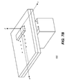
- FIG. 7B shows an isometric view of the RF transition module 600.
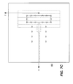
- FIG. 7C shows a plan view of the RF transition module 600.
- FIG. 7D shows an electromagnetic field distribution inside the RF transition module 600.
- the RF energy comes in along the stripline 602 (Port 1) and is coupled into the rectangular waveguide 604 (Port 2).
- the rectangular block 606 placed above the trace represents the dielectric material that is inserted in a can (not shown).
- the dielectric material 606 tunes the transition coupling performance by varying the material dielectric properties.
- the RF transition module comprises a stripline trace section with openings in the nearby ground planes forming a quarter-wavelength resonator.
- the RF energy from the stripline is electromagnetically coupled to either a rectangular wavelength piece or a coaxial contact.
- This RF transition module 600 is integrated in the beam-forming-network-printed-wiring-board.
- the rhombic shape beam forming network printed wiring board is shown in FIG. 1A .
- two RF transition modules are integrated with the phased array.
- the transition modules are responsible for combining the elements in one subarray.
- the subarray includes 256 elements.
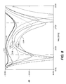
- FIG. 8 represents the results of a finite-element electromagnetic field simulation within the RF waveguide transition structure shown in FIG. 6 .
- the insert material simulated includes Teflon, Taconic, Rexolite, Rogers Duroid, and Arlon Coefficient of Linear Thermal Expansion (CLTE).
- CLTE Arlon Coefficient of Linear Thermal Expansion
- the insert material is simulated by varying its dielectric constant and the return losses for the RF transition are plotted as a function of the RF frequency. All materials within the numerical analysis result in a "double null" pattern across the frequency band of interest - this is a desirable characteristic because it means less reflection, better impedance matching, and wider bandwidth in the desired frequency range.
- FIG. 8 indicates that a return loss of 20 dB or better has been achieved over more than 2 GHz frequency range - better than 10% bandwidth at K-band (20 GHz). This is a significant improvement in operation bandwidth from previous designs.
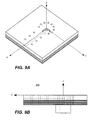
- FIGs. 9A and 9C show a perspective view and side view of a stripline to coaxial module 900 which also includes a coaxial interface.
- Figure 9B shows the performance of the stripline to waveguide module and the stripline to coaxial connector transition module
- transition modules display wide bandwidth while having a below -25 dB return loss.
- the waveguide transition module is less sensitive to trace width / length variance, representing manufacturing tolerance fluctuation.
- the above-identified modules are simpler structures and less costly than conventional transition modules.
- the new coaxial transition module is easier to manufacture thereby reducing the cost and the schedule risk associated with manufacturing of the beam forming network.
- a phased array antenna system in accordance with an embodiment expands the capabilities of phased array antenna systems in two critical areas: (1) providing a low observability compliant phased array aperture with reduced size, weight and cost; and (2) providing a beam forming network scalability to large full size arrays. Both capabilities allow for the enhanced phased array antennas utilized for a variety of applications.
Landscapes
- Engineering & Computer Science (AREA)
- Manufacturing & Machinery (AREA)
- Variable-Direction Aerials And Aerial Arrays (AREA)
Abstract
Description
- The present disclosure relates generally to beam forming networks and more particularly to phased array antennas utilizing such networks.
- Active phased array antenna systems are capable of forming one or more antenna beams of electromagnetic energy and electronically steering the beams to targets, with no mechanical moving parts involved. A phased array antenna system has many advantages over other types of mechanical antennas, such as dishes, in terms of beam steering agility and speed, low profiles, low observability, and low maintenance.
- A beam forming network is a major and critical part of a phased array antenna system. The beam forming network is responsible for collecting all the electromagnetic signals from the array antenna modules and combining them in a phase coherent way for the optimum antenna performance. The element spacing in a phased array is typically at one-half of the wavelength for electromagnetic waves in space.
- There are design challenges when utilizing a phased array antenna system. Firstly, it is important that the phased array include a rhombic shape of aperture for low observabilty requirements of the system. In addition, the system should be as small as possible to conserve space while still having the same performance characteristics of conventional shaped phased array antenna systems. Furthermore, as array antenna frequency increases, the element spacing decreases in an inversely proportional manner. Due to this tight spacing in phased arrays at microwave frequencies, transitions of radio frequency (RF) energy from inside of the beam forming network printed wiring board to the backside of the antenna have always been one of the critical RF design factors in phased array development. Conventional designs had tighter tolerances in the feature alignments of the RF transition, which limits the choice of suppliers for the systems and impacts the cost and schedule for producing the antennas as well.
- What is needed is a method and system to overcome the above-identified issues. One or more of the present embodiments address one or more of the above-identified needs and others.
- The features, functions, and advantages can be achieved independently in various embodiments of the present invention or may be combined in yet other embodiments.
- One or more systems and methods for forming phased array beams are disclosed. According to one embodiment, a phased array antenna system includes a printed wiring board formed in rhombic shape that accommodates requirements for low observability, a beam forming network located within the printed wiring board, wherein the beam forming network is located over substantially the entire printed wiring board, and a plurality of connectors located on the backside of the printed wiring board configured to allow for expansion of the system.
- According to another embodiment, a method for forming a phased array beam includes providing a printed wiring board formed in a rhombic shape, providing a beam forming network located within the printed wiring board, wherein the beam-forming network is located over substantially the entire printed wiring board, and providing a plurality of connectors only on the back side of the printed wiring board to allow for expansion of the phased array beams.
- According to another embodiment, a radio frequency "RF" transition system includes a stripline trace section with openings in ground planes and forms a quarter wavelength resonator, and an electromagnetic mechanism to couple the RF energy from the stripline trace section to a connector, wherein the RF signal energy is transferred from inside a beam forming network printed wiring board to an antenna back plane with minimal RF losses.
- According to another embodiment, a radio-frequency "RF" transition module includes a first port, a can coupled above the first port, the can including dielectric material therein; wherein the can tunes the transition module by varying the properties of the dielectric material, a connector coupled to the first port, and a second port coupled to the connector, wherein the transition modules provide RF signals to a phased array antenna system.
- According to another embodiment, a phased array antenna system includes a printed wiring board formed in rhombic shape that accommodates requirements for low observability, a beam forming network located within the printed wiring board, wherein the beam forming network is located over substantially the entire printed wiring board, a radio-frequency "RF" transition system comprising a stripline trace section with openings in ground planes and forms a quarter wavelength resonator; and an electromagnetic mechanism to couple the RF energy from the stripline trace section to a connector, wherein the RF signal energy is transferred from inside the printed wiring board to an antenna back plane with minimal RF losses, and a plurality of connectors located on the backside of the printed wiring board that allows for expansion of the system.
- According to another embodiment, a method for transferring radio-frequency "RF" signal energy includes forming a quarter-wavelength resonator, and coupling the RF signal energy from a stripline trace section to a connector, wherein the RF signal energy is transferred from inside a beam forming network printed wiring board to an antenna back plane with minimal RF losses.
-
-
FIG. 1A is a mechanical schematic of one embodiment of a beam forming network within a printed wiring distribution board which has a rhombic shape, according to an embodiment. -
FIG. 1B illustrates the layers associated with the printed wiring board ofFigure 1A . -
FIG. 2 is a mechanical schematic of the receive phased array antenna system with two subarrays of the beam forming network as shown inFig. 1A . -
FIG. 3A is a diagram view of the beam forming network RF circuits inside the beam former printed wiring board, according to an embodiment. -
FIG. 3B shows the octagonal arrangement of clock lines on the beam former printed wiring board, according to an embodiment. -
FIG. 3C shows the octagonal arrangement of data lines on the beam former printed wiring board, according to an embodiment. -
FIG. 4 is a diagram of a receive phased array antenna assembly, according to an embodiment. -
FIG. 5 illustrates the back side of the phased array antenna system that shows the back side connectors for DC power and logic, and the coaxial connectors for radio frequency (RF) signals, according to an embodiment. -
Figure 6 is a perspective view of a stripline to waveguide transition module in accordance with an embodiment. -
FIG. 7A shows a side view of an RF transition module, according to an embodiment. -
FIG. 7B shows an isometric view of the RF transition module. -
FIG. 7C shows a plan view of the RF transition module. -
FIG. 7D shows an electromagnetic field distribution inside the RF transition module. -
FIG. 8 represents the results of a finite-element electromagnetic field simulation within the waveguide transition module shown inFIG. 6 . -
FIG. 9A shows a perspective view of a stripline to coaxial module which also includes a coaxial interface. -
FIG. 9B shows a side view of the stripline to coaxial module which includes a coaxial interface. -
FIG 9C shows the performance comparison of the stripline to waveguide module and the stripline to coaxial module. - The present embodiment relates generally to beam forming networks and more particularly to phased array antennas utilizing such networks. The following description is presented to enable one of ordinary skill in the art to make and use the embodiment and is provided in the context of a patent application and its requirements. Various modifications to the embodiments and the generic principles and features described herein will be readily apparent to those skilled in the art. Thus, the present embodiment is not intended to be limited to the embodiments shown, but is to be accorded the widest scope consistent with the principles and features described herein.
- Every phased array antenna system includes a beam forming network to coherently combine the signals from all of its many elements. It is this signal combining ability that forms the electromagnetic beam. A beam forming distribution board for a conventional phased array antenna system has a rectangular shape for the beam forming network. As is known the rectangular shape provides problems because it is easily observable electronically due to its electronic signature. Hence it is desirable for the phased array antenna system to be rhombic in shape to allow for low observability.
- Active electronically scanned phased arrays have been produced that contain a large number of phased array elements. For example, The Boeing Company has produced such a phased array antenna system that contains 4,096 elements in 8 subarrays arranged in a 2x4 configuration.
- In a conventional receive phased array antenna system all of the DC power and logic interconnections are placed at the outside edges of the subarray. One cannot add more subarray columns to increase the size without having large gaps in-between adjacent subarrays. In conventional phased array antenna systems such as K-band arrays, the rhombic shape of aperture for phased array antennas were accomplished by either using the metal plate itself, (which offered only the minimum benefit to the low observability), or having passive dummy elements placed around the rectangular shape of active elements.
- There are four critical features in that distinguish the beam forming network of the present embodiment over conventional beam forming networks:
- (1) A rhombic shape of the beam forming network subarray that accommodates requirements for low observability and utilizes beam forming elements over substantially the entire array.
- (2) Reduced the column and row gaps in between the subarray panels, with improved results on the antenna beam patterns.
- (3) Improved RF bandwidth and mechanical tolerances in the RF transition from the beam forming network to the backside of the array.
- (4) Back side interconnections that allow the array architecture to expand to include more subarrays and thus more elements in a full size array.
- A phased array antenna system in accordance with an embodiment expands the capabilities of phased array antenna systems in two critical areas: (1) providing a low observability compliant phased array aperture with reduced size, weight and cost; and (2) providing a beam forming network scalability to large full- size arrays. Both capabilities allow for the enhanced phased array antennas utilized for a variety of applications. To describe the features of the phased array antenna system refer now to the following description in conjunction with the accompanying figures.
-
FIG. 1A is a mechanical schematic of one embodiment of abeam forming network 100 within a printedwiring board 102. Thebeam forming network 100 is formed inside a rhombic shape printed wiring board (PWB) 102, so that two or more of such identical boards can be put together to form a larger sized array without compromising the low observability characteristics. In this embodiment, the rhombic shape of the aperture is covered with active beam forming elements for a maximum cost effective benefit to the antenna system. In an embodiment, thePWB 102 includes nine layers as shown inFigure 1B . -
FIG. 2 is a mechanical schematic of the receive phasedarray antenna system 200 with twosubarrays FIG. 2 shows that theedge gaps 204 in-between the adjacent boards are of only one element spacing, as compared with two element spacing in the conventional phased arrays. This reduction in the gap width improves the antenna beam patterns. The reduction of gap width is accomplished by laying out the beam forming circuits of the subarrays 202a and 202b in a more efficient manner. Also, by placing all of the circuitry and connectors on the backside adjacent subarrays, the subarrays can be placed closer together than the subarrays utilized in a conventional phased array antenna system. -
FIG. 3A is a diagram of a portion of the beam formingnetwork circuits 200 inside thePWB 202.FIG. 3A shows stripline traces 302 on the RF layer 300 embedded inside the printedwiring board 202. These stripline traces 302 form the RF distribution network for the beam forming function. As is seen inFIGs. 3B and 3C , the data and clock lines are arranged in an orthogonal style to provide a more efficient layout on thePWB 202 and more robust signal integrity for array's beam steering control. - The array assembly and the backside interconnections for the phased array antenna system are shown in
FIG. 4 andFIG. 5 .FIG. 4 is a diagram of a receive phasedarray antenna assembly 400. In this embodiment onesubarray 410a is shown assembled and one subarray 410b is shown in exploded view. As is seen the subarray 410b includes a plurality ofsubarray elements 412, amodule shim 414, a multilayer wiring board (MLWB) 416, anelastomer connector shim 418 and a pressure plate withthermal transfer material 420. The MWLB is utilized advantageously to provide the RF, power and logic distribution for the phased array antenna. These elements are coupled together as shown insubarray 410a to provide the rhombic shaped array. -
FIG. 5 illustrates the back side of the phased array antenna system showing the back side connectors for DC/logic connector 502, and the RF portcoaxial connector 504 for the RF signals. By including these connectors on the back side of the board the subarrays can be placed closer together. The RF port connector provides for an RF transition for the beam forming network printed wiring board and the array housing. As before mentioned, in conventional subarrays, the connectors are placed on the sides of the PWB thereby causing adjacent subarrays to be placed at a distance from each other based upon the size of the connectors. In one embodiment there is one port per each subarray. A phased array antenna system in accordance with an embodiment expands the capabilities of phased array antenna systems in two critical areas: (1) providing a low observability compliant phased array aperture with reduced size, weight and cost; and (2) providing a beam forming network scalability to large full size arrays. Both capabilities allow for the enhanced phased array antennas utilized for a variety of applications. The embodiment includes a RF transition module that two key improvements over the previous RF transition modules: - (1) improved RF bandwidth with more tuning range by selecting the optimum material dielectric constant for the tuning block.
- (2) more relaxed mechanical tolerances in the RF transition from the beam forming network to the backside of the array, thus making the board more manufacturable, with lower cost. To describe the features of the RF transition module in more detail refer now to the following description in conjunction with the accompanying figures.
- The RF distribution network constructed inside the PWB for the beam forming function is shown in
FIG. 3A . The RF traces are connected at each 256-element level to thetransition module 600 shown above inFIG. 6 . -
FIG. 6 is a perspective view of a stripline to waveguideRF transition module 600 or system in accordance with one or more embodiments.FIG. 7A shows a side view of theRF transition module 600.FIG. 7B shows an isometric view of theRF transition module 600.FIG. 7C shows a plan view of theRF transition module 600.FIG. 7D shows an electromagnetic field distribution inside theRF transition module 600. As is seen, the RF energy comes in along the stripline 602 (Port 1) and is coupled into the rectangular waveguide 604 (Port 2). Therectangular block 606 placed above the trace represents the dielectric material that is inserted in a can (not shown). Thedielectric material 606 tunes the transition coupling performance by varying the material dielectric properties. In one embodiment, the RF transition module comprises a stripline trace section with openings in the nearby ground planes forming a quarter-wavelength resonator. The RF energy from the stripline is electromagnetically coupled to either a rectangular wavelength piece or a coaxial contact. - This
RF transition module 600 is integrated in the beam-forming-network-printed-wiring-board. The rhombic shape beam forming network printed wiring board is shown inFIG. 1A . Inside each PWB, two RF transition modules are integrated with the phased array. The transition modules are responsible for combining the elements in one subarray. In one embodiment the subarray includes 256 elements. -
FIG. 8 represents the results of a finite-element electromagnetic field simulation within the RF waveguide transition structure shown inFIG. 6 . The insert material simulated includes Teflon, Taconic, Rexolite, Rogers Duroid, and Arlon Coefficient of Linear Thermal Expansion (CLTE). The insert material is simulated by varying its dielectric constant and the return losses for the RF transition are plotted as a function of the RF frequency. All materials within the numerical analysis result in a "double null" pattern across the frequency band of interest - this is a desirable characteristic because it means less reflection, better impedance matching, and wider bandwidth in the desired frequency range.FIG. 8 indicates that a return loss of 20 dB or better has been achieved over more than 2 GHz frequency range - better than 10% bandwidth at K-band (20 GHz). This is a significant improvement in operation bandwidth from previous designs. - Another RF transition design comprising a low cost commercial off-the-shelf (COTS), surface mount coaxial connector has also been used for the same stripline matching network, i.e., the coaxial matching has been successfully simulated and compared. For the coaxial cases, the compact impedance match circuit occupies less than one-half the space as for the waveguide case. The waveguide transition module occupies four times the width, but about the same height as the coaxial connector.
FIGs. 9A and9C show a perspective view and side view of a stripline tocoaxial module 900 which also includes a coaxial interface.Figure 9B shows the performance of the stripline to waveguide module and the stripline to coaxial connector transition module - As is seen, desirable characteristics of these transition modules display wide bandwidth while having a below -25 dB return loss. The waveguide transition module is less sensitive to trace width / length variance, representing manufacturing tolerance fluctuation. Overall, the above-identified modules are simpler structures and less costly than conventional transition modules. Also, the new coaxial transition module is easier to manufacture thereby reducing the cost and the schedule risk associated with manufacturing of the beam forming network.
- A phased array antenna system in accordance with an embodiment expands the capabilities of phased array antenna systems in two critical areas: (1) providing a low observability compliant phased array aperture with reduced size, weight and cost; and (2) providing a beam forming network scalability to large full size arrays. Both capabilities allow for the enhanced phased array antennas utilized for a variety of applications.
- Although the present invention has been described in accordance with particular embodiments, one of ordinary skill in the art will readily recognize that there could be variations to the embodiments and those variations would be within the spirit and scope of the present invention. Accordingly, many modifications may be made by one of ordinary skill in the art without departing from the spirit and scope of the appended claims.
Claims (20)
- A phased array antenna system (200), comprising:a printed wiring board (102) formed in rhombic shape that accommodates requirements for low observability;a beam forming network (100) located within the printed wiring board, wherein the beam forming network is located over substantially the entire printed wiring board; anda plurality of connectors (502, 504) located on the backside of the printed wiring board configured to allow for expansion of the system.
- The phased array antenna system of claim 1, wherein the beam forming network includes at least one subarray (202a, 202b) of a plurality of beam forming elements, and wherein a non-active element gap (204) between at least two subarrays are minimized.
- The phased array antenna system of claim 2, wherein data and clock lines of the beam forming elements are arranged in an orthogonal style to provide an efficient layout of the printed wiring board and robust signal integrity for the array beam steering control, and wherein the subarray comprises a plurality of subarray elements (412), a module shim (414) coupled to the plurality of subarray elements, a multilayer wiring board (416) coupled to the module shim, a connector shim (418) coupled to the multilayer wiring board; and a pressure plate (420) coupled to the connector shim, wherein two or more subarrays are coupled together to provide a rhombic shaped array.
- A method for forming a phased array beam, the method comprising:providing a printed wiring board (102) formed in a rhombic shape;providing a beam forming network (100) located within the printed wiring board, wherein the beam-forming network is located over substantially the entire printed wiring board; andproviding a plurality of connectors (502, 504) only on the back side of the printed wiring board to allow for expansion of the phased array beams.
- The method of claim 4, wherein the beam forming network includes at least two subarrays (202a, 202b), each subarray having a plurality of beam forming elements, and wherein a non-active element gap (204) between the at least two subarrays is minimized.
- The method of claim 5, wherein data and clock lines of the beam forming elements are arranged in an orthogonal style to provide an efficient layout of the printed wiring board and robust signal integrity for the array beam steering control, and wherein each subarray comprises a plurality of subarray elements (412), a module shim (414) coupled to the plurality of subarray elements, a multilayer wiring board (416) coupled to the module shim, a connector shim (418) coupled to the multilayer wiring board; and a pressure plate (420) coupled to the connector shim, wherein two or more subarrays are coupled together to provide a rhombic shaped array.
- A radio frequency "RF" transition system (600), comprising:a stripline trace section (602) with openings in ground planes and forms a quarter wavelength resonator; andan electromagnetic mechanism (604) to couple the RF energy from the stripline trace section to a connector, wherein the RF signal energy is transferred from inside a beam forming network (100) printed wiring board (102) to an antenna back plane with minimal RF losses.
- The RF transition system of claim 7, wherein the connector comprises one of a rectangular waveguide and a coaxial contact.
- The RF transition system of claim 7, wherein the electromagnetic mechanism comprises a dielectric material (606) which is inserted in a can for tuning the transition system; wherein the coupling performance is a function of the material's dielectric properties.
- The RF transition system of claim 9, wherein the dielectric material is selected from a group consisting of Teflon, Taconic, Rexolite, Rogers Duroid and Arlon Coefficient of Linear Thermal Expansion "CLTE".
- The RF transition system of claim 9, wherein the dielectric material is selected such that there is little reflective good impedance matching and wide bandwidth in a desired frequency range.
- A radio-frequency "RF" transition module, comprising:a first port (602);a can coupled above the first port, the can including dielectric material (606) therein; wherein the can tunes the transition module by varying the properties of the dielectric material;a connector coupled to the first port; anda second port (604) coupled to the connector, wherein the transition modules provide RF signals to a phased array antenna system.
- The RF transition module of claim 12, wherein the connector comprises one of a wave guide and a coaxial contact.
- The RF transition module of claim 12, wherein the RF transition module is integrated in a beam forming printed wiring board (102).
- A phased array antenna system (200), comprising:a printed wiring board (102) formed in rhombic shape that accommodates requirements for low observability;a beam forming network (100) located within the printed wiring board, wherein the beam forming network is located over substantially the entire printed wiring board;a radio-frequency "RF" transition system (600) comprising a stripline trace section (602) with openings in ground planes and forms a quarter wavelength resonator; and an electromagnetic mechanism (604) to couple the RF energy from the stripline trace section to a connector, wherein the RF signal energy is transferred from inside the printed wiring board to an antenna back plane with minimal RF losses; anda plurality of connectors (502, 504) located on the backside of the printed wiring board that allows for expansion of the system.
- The phased array antenna system of claim 15, wherein the connector comprises one of a rectangular waveguide and a coaxial contact.
- The phased array antenna system of claim 15, wherein the electromagnetic mechanism comprises a dielectric material which is inserted in a can for tuning the transition system; wherein the coupling performance is a function of the material's dielectric properties.
- The phased array antenna system of claim 15, wherein the dielectric material is selected from a group consisting of Teflon, Taconic, Rexolite, Rogers Duroid and Arlon Coefficient of Linear Thermal Expansion "CLTE".
- A method for transferring radio-frequency "RF" signal energy, the method comprising:forming a quarter-wavelength resonator; andcoupling the RF signal energy from a stripline trace section (602) to a connector, wherein the RF signal energy is transferred from inside a beam forming network printed wiring board to an antenna back plane with minimal RF losses.
- The method of claim 19 wherein the coupling comprises inserting a dielectric material (606) in a can for tuning a transition system (200); wherein the coupling performance is a function of the material's dielectric properties, and wherein the dielectric material is selected from a group consisting of Teflon, Taconic, Rexolite, Rogers Duroid and Arlon Coefficient of Linear Thermal Expansion "CLTE".
Applications Claiming Priority (2)
| Application Number | Priority Date | Filing Date | Title |
|---|---|---|---|
| US11/767,170 US8154469B2 (en) | 2007-06-22 | 2007-06-22 | Radio frequency (RF) transition design for a phased array antenna system utilizing a beam forming network |
| US11/767,129 US7609210B2 (en) | 2007-06-22 | 2007-06-22 | Phased array antenna system utilizing a beam forming network |
Publications (3)
| Publication Number | Publication Date |
|---|---|
| EP2006956A2 true EP2006956A2 (en) | 2008-12-24 |
| EP2006956A3 EP2006956A3 (en) | 2009-02-11 |
| EP2006956B1 EP2006956B1 (en) | 2017-12-13 |
Family
ID=39798132
Family Applications (1)
| Application Number | Title | Priority Date | Filing Date |
|---|---|---|---|
| EP08252104.8A Not-in-force EP2006956B1 (en) | 2007-06-22 | 2008-06-19 | System and method for a radio frequency (RF) transition design for a phased array antenna system utilizing a beam forming network |
Country Status (1)
| Country | Link |
|---|---|
| EP (1) | EP2006956B1 (en) |
Cited By (4)
| Publication number | Priority date | Publication date | Assignee | Title |
|---|---|---|---|---|
| US7609210B2 (en) | 2007-06-22 | 2009-10-27 | Boeing Company | Phased array antenna system utilizing a beam forming network |
| WO2014005699A1 (en) * | 2012-07-03 | 2014-01-09 | Qest Quantenelektronische Systeme Gmbh | Antenna system for broadband satellite communication in the ghz frequency range, comprising a feeding arrangement |
| US9532234B2 (en) | 2013-06-28 | 2016-12-27 | Huawei Technologies Co., Ltd. | Multimode base station control method and base station |
| CN113824456A (en) * | 2021-09-14 | 2021-12-21 | 重庆两江卫星移动通信有限公司 | Active multi-beam tile-type phased array receiving assembly |
Citations (1)
| Publication number | Priority date | Publication date | Assignee | Title |
|---|---|---|---|---|
| WO2003049231A1 (en) | 2001-12-05 | 2003-06-12 | The Boeing Company | Phased array antenna system |
Family Cites Families (6)
| Publication number | Priority date | Publication date | Assignee | Title |
|---|---|---|---|---|
| GB865474A (en) * | 1958-08-25 | 1961-04-19 | Cossor Ltd A C | Improvements in and relating to radio frequency coupling devices |
| EP1221181A4 (en) * | 1999-09-02 | 2003-03-19 | Commw Scient Ind Res Org | SUPPLY STRUCTURE FOR ELECTROMAGNETIC WAVEGUIDES |
| US6606056B2 (en) * | 2001-11-19 | 2003-08-12 | The Boeing Company | Beam steering controller for a curved surface phased array antenna |
| GB0228233D0 (en) * | 2002-12-04 | 2003-01-08 | Astrium Ltd | Improvements relatings to antennas |
| US6975267B2 (en) * | 2003-02-05 | 2005-12-13 | Northrop Grumman Corporation | Low profile active electronically scanned antenna (AESA) for Ka-band radar systems |
| US7287987B2 (en) * | 2005-05-31 | 2007-10-30 | The Boeing Company | Electrical connector apparatus and method |
-
2008
- 2008-06-19 EP EP08252104.8A patent/EP2006956B1/en not_active Not-in-force
Patent Citations (1)
| Publication number | Priority date | Publication date | Assignee | Title |
|---|---|---|---|---|
| WO2003049231A1 (en) | 2001-12-05 | 2003-06-12 | The Boeing Company | Phased array antenna system |
Cited By (8)
| Publication number | Priority date | Publication date | Assignee | Title |
|---|---|---|---|---|
| US7609210B2 (en) | 2007-06-22 | 2009-10-27 | Boeing Company | Phased array antenna system utilizing a beam forming network |
| WO2014005699A1 (en) * | 2012-07-03 | 2014-01-09 | Qest Quantenelektronische Systeme Gmbh | Antenna system for broadband satellite communication in the ghz frequency range, comprising a feeding arrangement |
| US9660352B2 (en) | 2012-07-03 | 2017-05-23 | Lisa Draexlmaier Gmbh | Antenna system for broadband satellite communication in the GHz frequency range, comprising horn antennas with geometrical constrictions |
| US9716321B2 (en) | 2012-07-03 | 2017-07-25 | Lisa Draexlmaier Gmbh | Antenna system for broadband satellite communication in the GHz frequency range, comprising a feeding arrangement |
| US10211543B2 (en) | 2012-07-03 | 2019-02-19 | Lisa Draexlmaier Gmbh | Antenna system for broadband satellite communication in the GHz frequency range, comprising dielectrically filled horn antennas |
| US9532234B2 (en) | 2013-06-28 | 2016-12-27 | Huawei Technologies Co., Ltd. | Multimode base station control method and base station |
| CN113824456A (en) * | 2021-09-14 | 2021-12-21 | 重庆两江卫星移动通信有限公司 | Active multi-beam tile-type phased array receiving assembly |
| CN113824456B (en) * | 2021-09-14 | 2023-03-21 | 重庆两江卫星移动通信有限公司 | Active multi-beam tile-type phased array receiving assembly |
Also Published As
| Publication number | Publication date |
|---|---|
| EP2006956B1 (en) | 2017-12-13 |
| EP2006956A3 (en) | 2009-02-11 |
Similar Documents
| Publication | Publication Date | Title |
|---|---|---|
| US8154469B2 (en) | Radio frequency (RF) transition design for a phased array antenna system utilizing a beam forming network | |
| US7609210B2 (en) | Phased array antenna system utilizing a beam forming network | |
| EP3888186B1 (en) | Ridge gap waveguide and multilayer antenna array including the same | |
| US12009591B2 (en) | Electromagnetic band gap structure (EBG) | |
| US6507320B2 (en) | Cross slot antenna | |
| EP2329562B1 (en) | Multilayer metamaterial isolator | |
| US20050035825A1 (en) | Double-sided, edge-mounted stripline signal processing modules and modular network | |
| WO2004006387A1 (en) | Slot antenna | |
| US6326920B1 (en) | Sheet-metal antenna | |
| EP3240101B1 (en) | Radiofrequency interconnection between a printed circuit board and a waveguide | |
| CN110957574B (en) | A stripline-fed broadband millimeter-wave antenna unit | |
| US7289078B2 (en) | Millimeter wave antenna | |
| CN108134203B (en) | Large-unit-space wide-angle scanning phased array antenna based on electromagnetic band gap structure | |
| US20100033272A1 (en) | Apparatus and method for forming a bandgap surface and waveguide transition modules incorporating a bandgap surface | |
| EP2006956B1 (en) | System and method for a radio frequency (RF) transition design for a phased array antenna system utilizing a beam forming network | |
| EP1730810B1 (en) | High gain antenna for microwave frequencies | |
| CN215834716U (en) | A multi-layer structure millimeter wave antenna | |
| CN222927778U (en) | Dual-frenquency common bore antenna structure and antenna array | |
| Lupyna et al. | High-efficiency waveguide antenna with low-cost materials for radar sensors in LRR and SRR band | |
| CN113964489A (en) | Wide-angle scanning phased-array antenna based on bent gaps | |
| RU2795571C1 (en) | Dualpolarized wide-angle antenna array | |
| CN222601366U (en) | Millimeter wave radar antenna and radar apparatus | |
| CN115313032B (en) | Dual-frenquency common bore antenna | |
| EP1820235B1 (en) | A stripline arrangement and a method for production thereof | |
| KR102198378B1 (en) | Switched beam-forming antenna device and manufacturing method thereof |
Legal Events
| Date | Code | Title | Description |
|---|---|---|---|
| PUAI | Public reference made under article 153(3) epc to a published international application that has entered the european phase |
Free format text: ORIGINAL CODE: 0009012 |
|
| 17P | Request for examination filed |
Effective date: 20080619 |
|
| AK | Designated contracting states |
Kind code of ref document: A2 Designated state(s): AT BE BG CH CY CZ DE DK EE ES FI FR GB GR HR HU IE IS IT LI LT LU LV MC MT NL NO PL PT RO SE SI SK TR |
|
| AX | Request for extension of the european patent |
Extension state: AL BA MK RS |
|
| PUAL | Search report despatched |
Free format text: ORIGINAL CODE: 0009013 |
|
| AK | Designated contracting states |
Kind code of ref document: A3 Designated state(s): AT BE BG CH CY CZ DE DK EE ES FI FR GB GR HR HU IE IS IT LI LT LU LV MC MT NL NO PL PT RO SE SI SK TR |
|
| AX | Request for extension of the european patent |
Extension state: AL BA MK RS |
|
| 17Q | First examination report despatched |
Effective date: 20090904 |
|
| AKX | Designation fees paid |
Designated state(s): AT BE BG CH CY CZ DE DK EE ES FI FR GB GR HR HU IE IS IT LI LT LU LV MC MT NL NO PL PT RO SE SI SK TR |
|
| GRAP | Despatch of communication of intention to grant a patent |
Free format text: ORIGINAL CODE: EPIDOSNIGR1 |
|
| INTG | Intention to grant announced |
Effective date: 20170629 |
|
| GRAS | Grant fee paid |
Free format text: ORIGINAL CODE: EPIDOSNIGR3 |
|
| GRAA | (expected) grant |
Free format text: ORIGINAL CODE: 0009210 |
|
| AK | Designated contracting states |
Kind code of ref document: B1 Designated state(s): AT BE BG CH CY CZ DE DK EE ES FI FR GB GR HR HU IE IS IT LI LT LU LV MC MT NL NO PL PT RO SE SI SK TR |
|
| REG | Reference to a national code |
Ref country code: GB Ref legal event code: FG4D |
|
| REG | Reference to a national code |
Ref country code: AT Ref legal event code: REF Ref document number: 955208 Country of ref document: AT Kind code of ref document: T Effective date: 20171215 Ref country code: CH Ref legal event code: EP |
|
| REG | Reference to a national code |
Ref country code: IE Ref legal event code: FG4D |
|
| REG | Reference to a national code |
Ref country code: DE Ref legal event code: R096 Ref document number: 602008053322 Country of ref document: DE |
|
| REG | Reference to a national code |
Ref country code: NL Ref legal event code: MP Effective date: 20171213 |
|
| REG | Reference to a national code |
Ref country code: LT Ref legal event code: MG4D |
|
| PG25 | Lapsed in a contracting state [announced via postgrant information from national office to epo] |
Ref country code: FI Free format text: LAPSE BECAUSE OF FAILURE TO SUBMIT A TRANSLATION OF THE DESCRIPTION OR TO PAY THE FEE WITHIN THE PRESCRIBED TIME-LIMIT Effective date: 20171213 Ref country code: LT Free format text: LAPSE BECAUSE OF FAILURE TO SUBMIT A TRANSLATION OF THE DESCRIPTION OR TO PAY THE FEE WITHIN THE PRESCRIBED TIME-LIMIT Effective date: 20171213 Ref country code: SE Free format text: LAPSE BECAUSE OF FAILURE TO SUBMIT A TRANSLATION OF THE DESCRIPTION OR TO PAY THE FEE WITHIN THE PRESCRIBED TIME-LIMIT Effective date: 20171213 Ref country code: NO Free format text: LAPSE BECAUSE OF FAILURE TO SUBMIT A TRANSLATION OF THE DESCRIPTION OR TO PAY THE FEE WITHIN THE PRESCRIBED TIME-LIMIT Effective date: 20180313 |
|
| REG | Reference to a national code |
Ref country code: AT Ref legal event code: MK05 Ref document number: 955208 Country of ref document: AT Kind code of ref document: T Effective date: 20171213 |
|
| PG25 | Lapsed in a contracting state [announced via postgrant information from national office to epo] |
Ref country code: LV Free format text: LAPSE BECAUSE OF FAILURE TO SUBMIT A TRANSLATION OF THE DESCRIPTION OR TO PAY THE FEE WITHIN THE PRESCRIBED TIME-LIMIT Effective date: 20171213 Ref country code: GR Free format text: LAPSE BECAUSE OF FAILURE TO SUBMIT A TRANSLATION OF THE DESCRIPTION OR TO PAY THE FEE WITHIN THE PRESCRIBED TIME-LIMIT Effective date: 20180314 Ref country code: HR Free format text: LAPSE BECAUSE OF FAILURE TO SUBMIT A TRANSLATION OF THE DESCRIPTION OR TO PAY THE FEE WITHIN THE PRESCRIBED TIME-LIMIT Effective date: 20171213 Ref country code: BG Free format text: LAPSE BECAUSE OF FAILURE TO SUBMIT A TRANSLATION OF THE DESCRIPTION OR TO PAY THE FEE WITHIN THE PRESCRIBED TIME-LIMIT Effective date: 20180313 |
|
| REG | Reference to a national code |
Ref country code: FR Ref legal event code: PLFP Year of fee payment: 11 |
|
| PG25 | Lapsed in a contracting state [announced via postgrant information from national office to epo] |
Ref country code: NL Free format text: LAPSE BECAUSE OF FAILURE TO SUBMIT A TRANSLATION OF THE DESCRIPTION OR TO PAY THE FEE WITHIN THE PRESCRIBED TIME-LIMIT Effective date: 20171213 |
|
| PG25 | Lapsed in a contracting state [announced via postgrant information from national office to epo] |
Ref country code: CY Free format text: LAPSE BECAUSE OF FAILURE TO SUBMIT A TRANSLATION OF THE DESCRIPTION OR TO PAY THE FEE WITHIN THE PRESCRIBED TIME-LIMIT Effective date: 20171213 Ref country code: EE Free format text: LAPSE BECAUSE OF FAILURE TO SUBMIT A TRANSLATION OF THE DESCRIPTION OR TO PAY THE FEE WITHIN THE PRESCRIBED TIME-LIMIT Effective date: 20171213 Ref country code: CZ Free format text: LAPSE BECAUSE OF FAILURE TO SUBMIT A TRANSLATION OF THE DESCRIPTION OR TO PAY THE FEE WITHIN THE PRESCRIBED TIME-LIMIT Effective date: 20171213 Ref country code: SK Free format text: LAPSE BECAUSE OF FAILURE TO SUBMIT A TRANSLATION OF THE DESCRIPTION OR TO PAY THE FEE WITHIN THE PRESCRIBED TIME-LIMIT Effective date: 20171213 Ref country code: ES Free format text: LAPSE BECAUSE OF FAILURE TO SUBMIT A TRANSLATION OF THE DESCRIPTION OR TO PAY THE FEE WITHIN THE PRESCRIBED TIME-LIMIT Effective date: 20171213 |
|
| PG25 | Lapsed in a contracting state [announced via postgrant information from national office to epo] |
Ref country code: AT Free format text: LAPSE BECAUSE OF FAILURE TO SUBMIT A TRANSLATION OF THE DESCRIPTION OR TO PAY THE FEE WITHIN THE PRESCRIBED TIME-LIMIT Effective date: 20171213 Ref country code: IT Free format text: LAPSE BECAUSE OF FAILURE TO SUBMIT A TRANSLATION OF THE DESCRIPTION OR TO PAY THE FEE WITHIN THE PRESCRIBED TIME-LIMIT Effective date: 20171213 Ref country code: IS Free format text: LAPSE BECAUSE OF FAILURE TO SUBMIT A TRANSLATION OF THE DESCRIPTION OR TO PAY THE FEE WITHIN THE PRESCRIBED TIME-LIMIT Effective date: 20180413 Ref country code: RO Free format text: LAPSE BECAUSE OF FAILURE TO SUBMIT A TRANSLATION OF THE DESCRIPTION OR TO PAY THE FEE WITHIN THE PRESCRIBED TIME-LIMIT Effective date: 20171213 Ref country code: PL Free format text: LAPSE BECAUSE OF FAILURE TO SUBMIT A TRANSLATION OF THE DESCRIPTION OR TO PAY THE FEE WITHIN THE PRESCRIBED TIME-LIMIT Effective date: 20171213 |
|
| REG | Reference to a national code |
Ref country code: DE Ref legal event code: R097 Ref document number: 602008053322 Country of ref document: DE |
|
| PLBE | No opposition filed within time limit |
Free format text: ORIGINAL CODE: 0009261 |
|
| STAA | Information on the status of an ep patent application or granted ep patent |
Free format text: STATUS: NO OPPOSITION FILED WITHIN TIME LIMIT |
|
| 26N | No opposition filed |
Effective date: 20180914 |
|
| PG25 | Lapsed in a contracting state [announced via postgrant information from national office to epo] |
Ref country code: DK Free format text: LAPSE BECAUSE OF FAILURE TO SUBMIT A TRANSLATION OF THE DESCRIPTION OR TO PAY THE FEE WITHIN THE PRESCRIBED TIME-LIMIT Effective date: 20171213 |
|
| REG | Reference to a national code |
Ref country code: CH Ref legal event code: PL |
|
| PG25 | Lapsed in a contracting state [announced via postgrant information from national office to epo] |
Ref country code: SI Free format text: LAPSE BECAUSE OF FAILURE TO SUBMIT A TRANSLATION OF THE DESCRIPTION OR TO PAY THE FEE WITHIN THE PRESCRIBED TIME-LIMIT Effective date: 20171213 |
|
| REG | Reference to a national code |
Ref country code: BE Ref legal event code: MM Effective date: 20180630 |
|
| REG | Reference to a national code |
Ref country code: IE Ref legal event code: MM4A |
|
| PG25 | Lapsed in a contracting state [announced via postgrant information from national office to epo] |
Ref country code: LU Free format text: LAPSE BECAUSE OF NON-PAYMENT OF DUE FEES Effective date: 20180619 Ref country code: MC Free format text: LAPSE BECAUSE OF FAILURE TO SUBMIT A TRANSLATION OF THE DESCRIPTION OR TO PAY THE FEE WITHIN THE PRESCRIBED TIME-LIMIT Effective date: 20171213 |
|
| PG25 | Lapsed in a contracting state [announced via postgrant information from national office to epo] |
Ref country code: CH Free format text: LAPSE BECAUSE OF NON-PAYMENT OF DUE FEES Effective date: 20180630 Ref country code: LI Free format text: LAPSE BECAUSE OF NON-PAYMENT OF DUE FEES Effective date: 20180630 Ref country code: IE Free format text: LAPSE BECAUSE OF NON-PAYMENT OF DUE FEES Effective date: 20180619 |
|
| PG25 | Lapsed in a contracting state [announced via postgrant information from national office to epo] |
Ref country code: BE Free format text: LAPSE BECAUSE OF NON-PAYMENT OF DUE FEES Effective date: 20180630 |
|
| REG | Reference to a national code |
Ref country code: DE Ref legal event code: R082 Ref document number: 602008053322 Country of ref document: DE Representative=s name: MAIER, LL.M., MICHAEL C., DE Ref country code: DE Ref legal event code: R082 Ref document number: 602008053322 Country of ref document: DE Representative=s name: BOULT WADE TENNANT LLP, DE |
|
| PG25 | Lapsed in a contracting state [announced via postgrant information from national office to epo] |
Ref country code: MT Free format text: LAPSE BECAUSE OF NON-PAYMENT OF DUE FEES Effective date: 20180619 |
|
| REG | Reference to a national code |
Ref country code: DE Ref legal event code: R082 Ref document number: 602008053322 Country of ref document: DE Representative=s name: BOULT WADE TENNANT LLP, DE |
|
| PG25 | Lapsed in a contracting state [announced via postgrant information from national office to epo] |
Ref country code: TR Free format text: LAPSE BECAUSE OF FAILURE TO SUBMIT A TRANSLATION OF THE DESCRIPTION OR TO PAY THE FEE WITHIN THE PRESCRIBED TIME-LIMIT Effective date: 20171213 |
|
| PG25 | Lapsed in a contracting state [announced via postgrant information from national office to epo] |
Ref country code: HU Free format text: LAPSE BECAUSE OF FAILURE TO SUBMIT A TRANSLATION OF THE DESCRIPTION OR TO PAY THE FEE WITHIN THE PRESCRIBED TIME-LIMIT; INVALID AB INITIO Effective date: 20080619 Ref country code: PT Free format text: LAPSE BECAUSE OF FAILURE TO SUBMIT A TRANSLATION OF THE DESCRIPTION OR TO PAY THE FEE WITHIN THE PRESCRIBED TIME-LIMIT Effective date: 20171213 |
|
| PGFP | Annual fee paid to national office [announced via postgrant information from national office to epo] |
Ref country code: FR Payment date: 20200625 Year of fee payment: 13 Ref country code: DE Payment date: 20200629 Year of fee payment: 13 |
|
| PGFP | Annual fee paid to national office [announced via postgrant information from national office to epo] |
Ref country code: GB Payment date: 20200629 Year of fee payment: 13 |
|
| REG | Reference to a national code |
Ref country code: DE Ref legal event code: R119 Ref document number: 602008053322 Country of ref document: DE |
|
| GBPC | Gb: european patent ceased through non-payment of renewal fee |
Effective date: 20210619 |
|
| PG25 | Lapsed in a contracting state [announced via postgrant information from national office to epo] |
Ref country code: GB Free format text: LAPSE BECAUSE OF NON-PAYMENT OF DUE FEES Effective date: 20210619 Ref country code: DE Free format text: LAPSE BECAUSE OF NON-PAYMENT OF DUE FEES Effective date: 20220101 |
|
| PG25 | Lapsed in a contracting state [announced via postgrant information from national office to epo] |
Ref country code: FR Free format text: LAPSE BECAUSE OF NON-PAYMENT OF DUE FEES Effective date: 20210630 |