EP2005600B1 - Bias circuit for a radio frequency power-amplifier and method therefor - Google Patents
Bias circuit for a radio frequency power-amplifier and method therefor Download PDFInfo
- Publication number
- EP2005600B1 EP2005600B1 EP06761965.0A EP06761965A EP2005600B1 EP 2005600 B1 EP2005600 B1 EP 2005600B1 EP 06761965 A EP06761965 A EP 06761965A EP 2005600 B1 EP2005600 B1 EP 2005600B1
- Authority
- EP
- European Patent Office
- Prior art keywords
- power amplifier
- mode
- biasing
- current
- switch
- Prior art date
- Legal status (The legal status is an assumption and is not a legal conclusion. Google has not performed a legal analysis and makes no representation as to the accuracy of the status listed.)
- Ceased
Links
- 238000000034 method Methods 0.000 title claims description 19
- 238000004891 communication Methods 0.000 claims description 46
- 230000004044 response Effects 0.000 claims description 10
- 229920006395 saturated elastomer Polymers 0.000 claims description 7
- 230000003213 activating effect Effects 0.000 claims 1
- 238000005516 engineering process Methods 0.000 description 7
- 230000001413 cellular effect Effects 0.000 description 6
- 230000008859 change Effects 0.000 description 6
- 230000007704 transition Effects 0.000 description 5
- 238000010168 coupling process Methods 0.000 description 4
- 238000005859 coupling reaction Methods 0.000 description 4
- 238000013461 design Methods 0.000 description 4
- 230000007246 mechanism Effects 0.000 description 3
- 238000012545 processing Methods 0.000 description 3
- 239000004065 semiconductor Substances 0.000 description 3
- 230000010267 cellular communication Effects 0.000 description 2
- 230000008878 coupling Effects 0.000 description 2
- 238000004519 manufacturing process Methods 0.000 description 2
- 230000003190 augmentative effect Effects 0.000 description 1
- 230000005540 biological transmission Effects 0.000 description 1
- 238000006243 chemical reaction Methods 0.000 description 1
- 238000011161 development Methods 0.000 description 1
- 238000010586 diagram Methods 0.000 description 1
- 230000000694 effects Effects 0.000 description 1
- 238000001914 filtration Methods 0.000 description 1
- 238000002955 isolation Methods 0.000 description 1
- 238000010295 mobile communication Methods 0.000 description 1
- 230000008520 organization Effects 0.000 description 1
- 238000011160 research Methods 0.000 description 1
- 230000035945 sensitivity Effects 0.000 description 1
- 238000001228 spectrum Methods 0.000 description 1
- 230000036962 time dependent Effects 0.000 description 1
Images

Classifications
-
- H—ELECTRICITY
- H03—ELECTRONIC CIRCUITRY
- H03F—AMPLIFIERS
- H03F3/00—Amplifiers with only discharge tubes or only semiconductor devices as amplifying elements
- H03F3/20—Power amplifiers, e.g. Class B amplifiers, Class C amplifiers
- H03F3/24—Power amplifiers, e.g. Class B amplifiers, Class C amplifiers of transmitter output stages
-
- H—ELECTRICITY
- H03—ELECTRONIC CIRCUITRY
- H03F—AMPLIFIERS
- H03F1/00—Details of amplifiers with only discharge tubes, only semiconductor devices or only unspecified devices as amplifying elements
- H03F1/02—Modifications of amplifiers to raise the efficiency, e.g. gliding Class A stages, use of an auxiliary oscillation
- H03F1/0205—Modifications of amplifiers to raise the efficiency, e.g. gliding Class A stages, use of an auxiliary oscillation in transistor amplifiers
-
- H—ELECTRICITY
- H03—ELECTRONIC CIRCUITRY
- H03F—AMPLIFIERS
- H03F1/00—Details of amplifiers with only discharge tubes, only semiconductor devices or only unspecified devices as amplifying elements
- H03F1/02—Modifications of amplifiers to raise the efficiency, e.g. gliding Class A stages, use of an auxiliary oscillation
- H03F1/0205—Modifications of amplifiers to raise the efficiency, e.g. gliding Class A stages, use of an auxiliary oscillation in transistor amplifiers
- H03F1/0261—Modifications of amplifiers to raise the efficiency, e.g. gliding Class A stages, use of an auxiliary oscillation in transistor amplifiers with control of the polarisation voltage or current, e.g. gliding Class A
-
- H—ELECTRICITY
- H03—ELECTRONIC CIRCUITRY
- H03F—AMPLIFIERS
- H03F1/00—Details of amplifiers with only discharge tubes, only semiconductor devices or only unspecified devices as amplifying elements
- H03F1/30—Modifications of amplifiers to reduce influence of variations of temperature or supply voltage or other physical parameters
- H03F1/302—Modifications of amplifiers to reduce influence of variations of temperature or supply voltage or other physical parameters in bipolar transistor amplifiers
-
- H—ELECTRICITY
- H03—ELECTRONIC CIRCUITRY
- H03F—AMPLIFIERS
- H03F1/00—Details of amplifiers with only discharge tubes, only semiconductor devices or only unspecified devices as amplifying elements
- H03F1/30—Modifications of amplifiers to reduce influence of variations of temperature or supply voltage or other physical parameters
- H03F1/303—Modifications of amplifiers to reduce influence of variations of temperature or supply voltage or other physical parameters using a switching device
-
- H—ELECTRICITY
- H04—ELECTRIC COMMUNICATION TECHNIQUE
- H04B—TRANSMISSION
- H04B1/00—Details of transmission systems, not covered by a single one of groups H04B3/00 - H04B13/00; Details of transmission systems not characterised by the medium used for transmission
- H04B1/005—Details of transmission systems, not covered by a single one of groups H04B3/00 - H04B13/00; Details of transmission systems not characterised by the medium used for transmission adapting radio receivers, transmitters andtransceivers for operation on two or more bands, i.e. frequency ranges
- H04B1/0053—Details of transmission systems, not covered by a single one of groups H04B3/00 - H04B13/00; Details of transmission systems not characterised by the medium used for transmission adapting radio receivers, transmitters andtransceivers for operation on two or more bands, i.e. frequency ranges with common antenna for more than one band
- H04B1/006—Details of transmission systems, not covered by a single one of groups H04B3/00 - H04B13/00; Details of transmission systems not characterised by the medium used for transmission adapting radio receivers, transmitters andtransceivers for operation on two or more bands, i.e. frequency ranges with common antenna for more than one band using switches for selecting the desired band
-
- H—ELECTRICITY
- H04—ELECTRIC COMMUNICATION TECHNIQUE
- H04B—TRANSMISSION
- H04B1/00—Details of transmission systems, not covered by a single one of groups H04B3/00 - H04B13/00; Details of transmission systems not characterised by the medium used for transmission
- H04B1/02—Transmitters
- H04B1/04—Circuits
-
- H—ELECTRICITY
- H03—ELECTRONIC CIRCUITRY
- H03F—AMPLIFIERS
- H03F2200/00—Indexing scheme relating to amplifiers
- H03F2200/27—A biasing circuit node being switched in an amplifier circuit
-
- H—ELECTRICITY
- H04—ELECTRIC COMMUNICATION TECHNIQUE
- H04B—TRANSMISSION
- H04B1/00—Details of transmission systems, not covered by a single one of groups H04B3/00 - H04B13/00; Details of transmission systems not characterised by the medium used for transmission
- H04B1/02—Transmitters
- H04B1/04—Circuits
- H04B2001/0408—Circuits with power amplifiers
Definitions
- One embodiment of the present invention relates to a bias circuit and method for biasing radio frequency (RF) and microwave power amplifiers (PAs), suitable for telecommunication applications.
- the invention is applicable to, but not limited to, a bias circuit and method of biasing a PA to transition between biasing in a current-mode of operation and a voltage-mode of operation on the same integrated circuit die.
- Wireless communication systems typically provide for radio telecommunication links to be arranged between a plurality of base transceiver stations (BTS) and a plurality of subscriber units.
- BTS base transceiver stations
- GSM Global System for Mobile Communications
- GSM is often referred to as 2 nd generation cellular technology and utilises constant envelope Gaussian Minimum Shift Keying (GMSK) modulation.
- GMSK constant envelope Gaussian Minimum Shift Keying
- GPRS General Packet Radio System
- GSM Global System for Mobile communications
- EDGE Enhanced Data Rate for Global Evolution
- GPRS Enhanced GPRS
- UMTS universal mobile telecommunication system
- UMTS is intended to provide a harmonised standard under which cellular radio communication networks and systems will provide enhanced levels of interfacing and compatibility with many other types of communication systems and networks, including fixed communication systems such as the Internet. Due to this increased complexity, as well as the features and services that it supports; UMTS is often referred to as a third generation (3G) cellular communication technology.
- 3G third generation
- a primary focus of the present invention is the field of radio frequency (RF) and microwave power amplifiers for use in telecommunication applications.
- RF radio frequency
- Continuing pressure on the limited spectrum available for radio communication systems is forcing the development of spectrally-efficient linear modulation schemes. Since the envelopes of a number of these 'linear' modulation schemes fluctuate, intermodulation products can be generated in the non-linear power amplifier. This results in the average power being delivered to the antenna being significantly lower than the maximum power, leading to poor efficiency of the power amplifier.
- 3G technology in addition to Edge, utilises non-constant envelope modulation.
- a biasing current source composed of a reference voltage 140, and a series resistor 155 is operably coupled to an input port of the power amplifier device 105 via a current-to-voltage converter.
- the current-to-voltage converter comprises a follower transistor 125 arranged to provide a low impedance to the base of reference transistor 145, that receives a current from current source 140, 155.
- the current from the biasing current source 140, 155 flows into reference transistor 145 and generates a voltage, which is supplied to the base of the PA device 105.
- the current source is coupled to the input port of the PA device 105, via the current-to-voltage converter, thereby biasing the PA 105 in a 'voltage-controlled' mode of operation.
- This design is termed an 'Augmented emitter follower'.
- the bias circuit comprises a biasing current source providing a current 205 to an input port of the power amplifier device 215 via base impedance 210.
- the input port of the PA device 215 comprises capacitive coupling 222 to the radio frequency input signal 224.
- the current source directly sets the current applied to the (base) input port of the PA device 215, thereby biasing the PA in a current-controlled mode of operation.
- PA Power Amplifier
- US 6873211 B1 discloses a circuit arrangement including a multi-mode bias circuit having a control voltage input, a mode control input for selecting between a linear mode and a saturation mode, and a bias output.
- US 2006/046666 A1 discloses a transmitter high in efficiency, good in linearity and capable of covering an output level in a wide range.
- embodiments of the present invention relate to a bias circuit for a Power Amplifier (PA) for a wireless communication unit and more particularly to a bias circuit capable of operating the PA both in saturated mode (e.g. in accordance with the GSM standard) and in a linear mode (e.g. in accordance with the EDGE or wideband code division multiple access (WCDMA) standard).
- a bias circuit and method of operation therefor are described to facilitate transitioning between biasing a Power Amplifier (PA) in current-mode and in voltage-mode.
- the bias circuit and method of operation therefor can advantageously be readily implemented within the same integrated circuit die.
- One embodiment of the present invention will be described in terms of a wireless subscriber communication unit.
- inventive concept herein described may be embodied in any wireless communication unit, such as a base station, where at least two modes of operation are supported, for example a first mode that is constant envelope modulation and a second non-constant envelope modulation mode.
- inventive concept can be applied to any type of power amplifier design where a transition between voltage-mode biasing and current-mode biasing may be desirable.
- FIG. 3 a block diagram of a wireless communication unit (for example a mobile subscriber unit (MS) in the context of cellular communications) is shown, adapted in accordance with embodiments of the present invention.
- a wireless communication unit for example a mobile subscriber unit (MS) in the context of cellular communications
- MS mobile subscriber unit
- the MS 300 contains an antenna 302 typically coupled to a duplex filter or antenna switch 304 that provides isolation between receive and transmit chains within the MS 300.
- the receiver chain includes receiver front-end circuit 306 (effectively providing reception, filtering and intermediate or base-band frequency conversion).
- the front-end circuit 306 is serially coupled to a signal processing function 308.
- An output from the signal processing function 308 is provided to a suitable output device 310, such as a screen or flat panel display.
- the receiver chain also includes received signal strength indicator (RSSI) circuitry 312, which in turn is coupled to a controller 314 that maintains overall subscriber unit control.
- the controller 314 may therefore receive bit error rate (BER) or frame error rate (FER) data from recovered information.
- BER bit error rate
- FER frame error rate
- the controller 314 is also coupled to the receiver front-end circuitry 306 and the signal processing function 308 (generally realised by a digital signal processor (DSP)).
- the controller is also coupled to a memory device 316 that selectively stores operating regimes, such as decoding/encoding functions, synchronisation patterns, code sequences, RSSI data, direction of arrival of a received signal and the like.
- the memory device 316 stores configuration settings primarily in the form of control signals to be applied to bias circuit switches, to open or close the respective switches, in response to the mode of operation of the wireless communication unit.
- the stored configuration settings enable the wireless communication unit to readily transition between voltage-mode biasing and current-mode biasing of the PA.
- a timer 318 is operably coupled to the controller 314 to control the timing of operations (transmission or reception of time-dependent signals), particularly with respect to timing of control signals applied to the switches in the bias circuit 350 within the MS 300.
- this essentially includes an input device 320, such as a keypad, coupled in series through transmitter/modulation circuitry 322 and a power amplifier 324 to the antenna 302.
- the transmitter/ modulation circuitry 322 and the power amplifier 324 are operationally responsive to the controller 314.
- the controller 314 is adapted to modify the configuration of the bias circuit 350 in response to the mode of operation of the MS 300, as described below with respect to FIG. 4 .
- bias circuit 350 that facilitates the transitioning between voltage-mode biasing and current-mode biasing of a power-amplifier 324, in response to control signals from a controller 314, in accordance with embodiments of the present invention.
- the bias circuit 350 comprises a biasing current source 402 operably coupled, in a first current path, to an input port of the power amplifier device 324 via a first switch 416.
- the configuration of the first switch is controlled by controller 314.
- the input port of the PA device 324 comprises capacitive coupling 422 to the radio frequency input signal 424.
- the input port comprises base impedance 418 and capacitive de-coupling 420, where the first switch 416 is operably coupled to the junction of the base impedance 418 and capacitive de-coupling 420.
- the current source is coupled to the input port of the PA device 324, thereby biasing the PA in a 'current-controlled' mode of operation.
- the biasing current source 402 is also operably coupled, in a second current path, to an input port of the power amplifier device 324 via a current-to-voltage converter 404 and third switch 414.
- the current-to-voltage converter 404 comprises a follower transistor 400, a reference transistor 410, and reference base impedance 426.
- the follower transistor 400 provides a low impedance to the base of reference transistor 410, receiving a current from current source 402.
- the current source is operably coupled to the reference transistor 410 via a second switch 408.
- the reference base impedance 426 balances the base impedance 418.
- the emitter port of the reference transistor 410 may be grounded, say via an impedance, as known in the art.
- the current from the biasing current source 402 flows into reference transistor 410, which generates a base voltage that is supplied to the base of the PA device through the reference base impedance and the third switch 414.
- two current sources could be used, one for either mode, in contrast to the embodiment described that utilises a single current source for both modes of operation.
- impedances may be operably coupled to the base ports of the transistors, such as base impedance 418 coupled to the base port of the PA device 324.
- the configuration of the second switch 408 and third switch 414 are also controlled by controller 314.
- controller 314 is operably coupled to a number of switches, where the configuration of the respective switches supports either current-mode biasing, or voltage-mode biasing. That is when controller 314 closes the second switch 408 and third switch 414, and opens first switch 416, the controller transitions (re-configures) the bias circuit 350 to voltage-mode biasing.
- controller 314 opens the second switch 408 and third switch 414, and closes first switch 416, the controller transitions (i.e. re-configures) the bias circuit 350 to current-mode biasing.
- the controller 314 configures the switches to support current-biasing, thereby solving the problem of dependency of the PA response to input power.
- the controller 314 configures the switches to support voltage-biasing, thereby providing a linear PA output.
- an integrated circuit manufacturer may manufacture a bias circuit (which may in some embodiments include other circuits as would be appreciated by a skilled person) that comprises at least one input control pin that is coupleable to the microcontroller 314 and comprises the aforementioned circuit elements up to the PA and its RF input.
- the bias control current source may be provided within the bias circuit IC or the bias control current source may be directly input to a 'current source input' of the bias circuit IC.
- embodiments of the present invention support having both biasing modes available on the same integrated circuit (IC) die.
- the two operating modes are selectable by a simple logic level input, for example using an inverter coupled to second and third switches to differentiate their configuration from the first switch. In this manner, the transitioning between current-mode biasing and voltage-mode biasing can be controlled by applying different logic values to a single IC pin.
- the aforementioned bias circuit biasing a PA reduces the sensitivity of the power amplifier performance to the range of input power (P in ) levels.
- the base current in current-controlled mode, the base current is constrained and therefore varying the input power has little impact on output power.
- the base current in a voltage-controlled mode, the base current is unlimited and varies with input power.
- the aforementioned arrangement may be utilised in later stages or across multiple stages, depending upon the design considerations, performance criteria and circuit elements prevalent at the time.
- a method 500 of transitioning between voltage and current biasing of a power-amplifier is illustrated, in accordance with embodiments of the present invention.
- the method commences with the wireless communication unit switching on, in step 505.
- a determination is then made as to whether the communication unit is to operate with a constant envelope modulation scheme or non-constant envelope modulation scheme, as shown in step 510.
- Such a determination may utilise a default operating mode in the wireless communication unit, for example where the user typically operates in a current-mode biasing mode for a coverage area supported by GSM.
- the determination may be made based on a preferred operating mode of a user of the wireless communication unit, for example that the user typically uses multimedia services supported by UMTS.
- the controller (say controller 314 of FIG. 3 ) opens second and third switches (switches 408, 414 in FIG. 4 ) and closes the first switch (switch 416 in FIG. 4 ), as in step 515.
- the power amplifier is then configured to operate in saturated mode, via configuration of the bias circuit, as shown in step 520.
- the controller (say controller 314 of FIG. 3 ) closes second and third switches (switches 408, 414 in FIG. 4 ) and opens the first switch (switch 416 in FIG. 4 ), as in step 530.
- the power amplifier is then configured to operate in a linear mode, via configuration of the bias circuit, as shown in step 535.
- the controller of the wireless communication unit is able to re-configure the bias circuit to support different modulation schemes via reconfiguring the operating mode of the power amplifier device.
- the improved biasing circuit and method for biasing a PA aims to provide at least one or more of the following advantages:
- aspects of the invention may be implemented in any suitable form including hardware, software, firmware or any combination of these.
- the elements and components of an embodiment of the invention may be physically, functionally and logically implemented in any suitable way. Indeed, although embodiments of the present invention have been described where the functionality may be implemented in a single unit or IC, it is envisaged that in other embodiments the circuit functionality may be implemented in a plurality of units or ICs or as part of other functional units.
- inventive concept can be applied by a semiconductor manufacturer to any integrated circuit comprising a power amplifier biasing circuit, for example those of the FreescaleTM power amplifier device family. It is further envisaged that, for example, a semiconductor manufacturer may employ the inventive concept in a design of a stand-alone device or application-specific integrated circuit (ASIC) and/or any other sub-system element.
- ASIC application-specific integrated circuit
- embodiments of the present invention describe a wireless communication unit having a PA and bias circuit therefor, an integrated circuit comprising a bias circuit and method for biasing a PA that support transitioning between a current-mode and a voltage-mode of biasing the Power Amplifier (PA), wherein the aforementioned disadvantages with prior art arrangements have been substantially alleviated.
- PA Power Amplifier
Landscapes
- Engineering & Computer Science (AREA)
- Power Engineering (AREA)
- Computer Networks & Wireless Communication (AREA)
- Signal Processing (AREA)
- Amplifiers (AREA)
Description
- One embodiment of the present invention relates to a bias circuit and method for biasing radio frequency (RF) and microwave power amplifiers (PAs), suitable for telecommunication applications. The invention is applicable to, but not limited to, a bias circuit and method of biasing a PA to transition between biasing in a current-mode of operation and a voltage-mode of operation on the same integrated circuit die.
- Wireless communication systems, for example cellular telephony or private mobile radio communication systems, typically provide for radio telecommunication links to be arranged between a plurality of base transceiver stations (BTS) and a plurality of subscriber units. An established harmonised cellular radio communication system, providing predominantly speech and short-data communication, is the Global System for Mobile Communications (GSM) . GSM is often referred to as 2nd generation cellular technology and utilises constant envelope Gaussian Minimum Shift Keying (GMSK) modulation.
- An enhancement to this cellular technology, termed the General Packet Radio System (GPRS), has been developed. GPRS provides packet switched technology on GSM's switched-circuit cellular platform. A yet further enhancement to GSM, which has been developed to improve system capacity can be found in the recently standardised Enhanced Data Rate for Global Evolution (EDGE) that encompasses Enhanced GPRS (EGPRS). A still yet further harmonised wireless communication system currently being defined is the universal mobile telecommunication system (UMTS). UMTS is intended to provide a harmonised standard under which cellular radio communication networks and systems will provide enhanced levels of interfacing and compatibility with many other types of communication systems and networks, including fixed communication systems such as the Internet. Due to this increased complexity, as well as the features and services that it supports; UMTS is often referred to as a third generation (3G) cellular communication technology.
- A primary focus of the present invention is the field of radio frequency (RF) and microwave power amplifiers for use in telecommunication applications. Continuing pressure on the limited spectrum available for radio communication systems is forcing the development of spectrally-efficient linear modulation schemes. Since the envelopes of a number of these 'linear' modulation schemes fluctuate, intermodulation products can be generated in the non-linear power amplifier. This results in the average power being delivered to the antenna being significantly lower than the maximum power, leading to poor efficiency of the power amplifier. Specifically, in this field, there has been a significant amount of research effort in developing high efficiency topologies capable of providing high performances in the 'back-off' (linear) region of the power amplifier. 3G technology, in addition to Edge, utilises non-constant envelope modulation.
- There are two known mechanisms for biasing the power amplifier (PA) in such wireless communication applications:
- (i) Voltage-mode biasing. Voltage-mode biasing is typically used for PAs operating in a linear mode, for example to support linearity requirements of non constant envelope signals; and
- (ii) Current-mode biasing. Current mode biasing is typically used for PAs operating in a 'saturated' mode, for example to support GSM communications. A current-biasing mode of operation is used in this regard to solve the problem of dependency of the PA response to input power.
- Referring now to
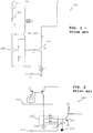
FIG. 1 , a knowncircuit 100 for voltage-mode biasing of a Power amplifier is illustrated. A biasing current source composed of areference voltage 140, and aseries resistor 155 is operably coupled to an input port of thepower amplifier device 105 via a current-to-voltage converter. The current-to-voltage converter comprises afollower transistor 125 arranged to provide a low impedance to the base ofreference transistor 145, that receives a current fromcurrent source current source reference transistor 145 and generates a voltage, which is supplied to the base of thePA device 105. - Thus, in this manner, the current source is coupled to the input port of the
PA device 105, via the current-to-voltage converter, thereby biasing thePA 105 in a 'voltage-controlled' mode of operation. This design is termed an 'Augmented emitter follower'. - Referring now to
FIG. 2 , a knownalternative circuit 200 for biasing a power amplifier in a current-mode of operation is illustrated. The bias circuit comprises a biasing current source providing a current 205 to an input port of thepower amplifier device 215 viabase impedance 210. The input port of thePA device 215 comprisescapacitive coupling 222 to the radiofrequency input signal 224. Thus, the current source directly sets the current applied to the (base) input port of thePA device 215, thereby biasing the PA in a current-controlled mode of operation. - There has been a recent trend for subscriber unit manufacturers, and consequently the semiconductor manufacturers designing integrated circuits to support the technologies implemented in the subscriber units, to offer dual-mode or multi-mode operation. In this regard, the subscriber unit and associated integrated circuits are capable of switching between operational modes in accordance with, say, user-requirements of services or features that they want to use. Often these dual-mode or multi-mode operations conflict from a technology perspective and separate circuitry is then required to support the individual modes. In order to support both constant-envelope modulation schemes and non-constant envelope modulation schemes, a wireless communication unit would currently require separate current-mode and voltage-mode bias circuits.
- Thus, a need exists for providing a power amplifier bias circuit, integrated circuit and method for biasing a Power Amplifier (PA).
-
US 6873211 B1 discloses a circuit arrangement including a multi-mode bias circuit having a control voltage input, a mode control input for selecting between a linear mode and a saturation mode, and a bias output.US 2006/046666 A1 discloses a transmitter high in efficiency, good in linearity and capable of covering an output level in a wide range. - We disclose a wireless communication unit, an integrated circuit comprising a bias circuit for biasing a Power Amplifier (PA) and a method of biasing therefor, as defined in the appended Claims.
-
-
FIG. 1 illustrates a known mechanism to bias a Power Amplifier in a voltage-mode of operation. -
FIG. 2 illustrates a known mechanism to bias a Power Amplifier in a current-mode of operation.
Exemplary embodiments of the present invention will now be described, by way of example only, with reference to the accompanying drawings, in which:-
FIG. 3 illustrates a wireless communication unit adapted in accordance with embodiments of the present invention; -
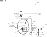
FIG. 4 illustrates a single circuit providing both voltage and current biasing of a power-amplifier in accordance with one embodiment of the present invention; and -
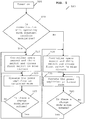
FIG. 5 illustrates a method of transitioning between voltage and current biasing of a power-amplifier in accordance with one embodiment of the present invention.
-
- In summary, embodiments of the present invention relate to a bias circuit for a Power Amplifier (PA) for a wireless communication unit and more particularly to a bias circuit capable of operating the PA both in saturated mode (e.g. in accordance with the GSM standard) and in a linear mode (e.g. in accordance with the EDGE or wideband code division multiple access (WCDMA) standard). In this regard, a bias circuit and method of operation therefor are described to facilitate transitioning between biasing a Power Amplifier (PA) in current-mode and in voltage-mode. Notably, the bias circuit and method of operation therefor can advantageously be readily implemented within the same integrated circuit die.
- One embodiment of the present invention will be described in terms of a wireless subscriber communication unit. However, it will be appreciated by a skilled artisan that the inventive concept herein described may be embodied in any wireless communication unit, such as a base station, where at least two modes of operation are supported, for example a first mode that is constant envelope modulation and a second non-constant envelope modulation mode. Furthermore, the inventive concept can be applied to any type of power amplifier design where a transition between voltage-mode biasing and current-mode biasing may be desirable.
- Referring now to
FIG. 3 , a block diagram of a wireless communication unit (for example a mobile subscriber unit (MS) in the context of cellular communications) is shown, adapted in accordance with embodiments of the present invention. - The MS 300 contains an
antenna 302 typically coupled to a duplex filter orantenna switch 304 that provides isolation between receive and transmit chains within theMS 300. For completeness, the receiver chain, as known in the art, includes receiver front-end circuit 306 (effectively providing reception, filtering and intermediate or base-band frequency conversion). The front-end circuit 306 is serially coupled to asignal processing function 308. An output from thesignal processing function 308 is provided to asuitable output device 310, such as a screen or flat panel display. The receiver chain also includes received signal strength indicator (RSSI)circuitry 312, which in turn is coupled to acontroller 314 that maintains overall subscriber unit control. Thecontroller 314 may therefore receive bit error rate (BER) or frame error rate (FER) data from recovered information. Thecontroller 314 is also coupled to the receiver front-end circuitry 306 and the signal processing function 308 (generally realised by a digital signal processor (DSP)). The controller is also coupled to amemory device 316 that selectively stores operating regimes, such as decoding/encoding functions, synchronisation patterns, code sequences, RSSI data, direction of arrival of a received signal and the like. - In accordance with embodiments of the invention, the
memory device 316 stores configuration settings primarily in the form of control signals to be applied to bias circuit switches, to open or close the respective switches, in response to the mode of operation of the wireless communication unit. In particular, the stored configuration settings enable the wireless communication unit to readily transition between voltage-mode biasing and current-mode biasing of the PA. Furthermore, atimer 318 is operably coupled to thecontroller 314 to control the timing of operations (transmission or reception of time-dependent signals), particularly with respect to timing of control signals applied to the switches in thebias circuit 350 within theMS 300. - As regards the transmit chain, this essentially includes an
input device 320, such as a keypad, coupled in series through transmitter/modulation circuitry 322 and apower amplifier 324 to theantenna 302. The transmitter/modulation circuitry 322 and thepower amplifier 324 are operationally responsive to thecontroller 314. Indeed, in accordance with embodiments of the present invention, thecontroller 314 is adapted to modify the configuration of thebias circuit 350 in response to the mode of operation of theMS 300, as described below with respect toFIG. 4 . - Referring now to
FIG. 4 , anexemplary bias circuit 350 is illustrated that facilitates the transitioning between voltage-mode biasing and current-mode biasing of a power-amplifier 324, in response to control signals from acontroller 314, in accordance with embodiments of the present invention. Thebias circuit 350 comprises a biasingcurrent source 402 operably coupled, in a first current path, to an input port of thepower amplifier device 324 via afirst switch 416. The configuration of the first switch is controlled bycontroller 314. The input port of thePA device 324 comprisescapacitive coupling 422 to the radiofrequency input signal 424. The input port comprisesbase impedance 418 andcapacitive de-coupling 420, where thefirst switch 416 is operably coupled to the junction of thebase impedance 418 andcapacitive de-coupling 420. Thus, when thefirst switch 416 is closed by thecontroller 314, the current source is coupled to the input port of thePA device 324, thereby biasing the PA in a 'current-controlled' mode of operation. - The biasing
current source 402 is also operably coupled, in a second current path, to an input port of thepower amplifier device 324 via a current-to-voltage converter 404 andthird switch 414. The current-to-voltage converter 404 comprises afollower transistor 400, areference transistor 410, andreference base impedance 426. Thefollower transistor 400 provides a low impedance to the base ofreference transistor 410, receiving a current fromcurrent source 402. The current source is operably coupled to thereference transistor 410 via asecond switch 408. Thereference base impedance 426 balances thebase impedance 418. The emitter port of thereference transistor 410 may be grounded, say via an impedance, as known in the art. The current from the biasingcurrent source 402 flows intoreference transistor 410, which generates a base voltage that is supplied to the base of the PA device through the reference base impedance and thethird switch 414. - In one embodiment of the present invention, it is envisaged that two current sources could be used, one for either mode, in contrast to the embodiment described that utilises a single current source for both modes of operation.
- In embodiments of the present invention, impedances may be operably coupled to the base ports of the transistors, such as
base impedance 418 coupled to the base port of thePA device 324. The configuration of thesecond switch 408 andthird switch 414 are also controlled bycontroller 314. - In summary,
controller 314 is operably coupled to a number of switches, where the configuration of the respective switches supports either current-mode biasing, or voltage-mode biasing. That is whencontroller 314 closes thesecond switch 408 andthird switch 414, and opensfirst switch 416, the controller transitions (re-configures) thebias circuit 350 to voltage-mode biasing. - Furthermore, when
controller 314 opens thesecond switch 408 andthird switch 414, and closesfirst switch 416, the controller transitions (i.e. re-configures) thebias circuit 350 to current-mode biasing. - In this manner, when the wireless communication unit is operating in GSM mode, i.e. the PA is operating in a saturated mode, the
controller 314 configures the switches to support current-biasing, thereby solving the problem of dependency of the PA response to input power. - In contrast, when the wireless communication unit is operating in a linear mode, for example supporting non constant envelope modulation schemes, such as those required for Edge or (3G) WCDMA applications, the
controller 314 configures the switches to support voltage-biasing, thereby providing a linear PA output. - It is envisaged that an integrated circuit manufacturer may manufacture a bias circuit (which may in some embodiments include other circuits as would be appreciated by a skilled person) that comprises at least one input control pin that is coupleable to the
microcontroller 314 and comprises the aforementioned circuit elements up to the PA and its RF input. In some embodiments, the bias control current source may be provided within the bias circuit IC or the bias control current source may be directly input to a 'current source input' of the bias circuit IC. - Advantageously, embodiments of the present invention support having both biasing modes available on the same integrated circuit (IC) die. In one embodiment of the present invention, the two operating modes are selectable by a simple logic level input, for example using an inverter coupled to second and third switches to differentiate their configuration from the first switch. In this manner, the transitioning between current-mode biasing and voltage-mode biasing can be controlled by applying different logic values to a single IC pin.
- Advantageously, the aforementioned bias circuit biasing a PA reduces the sensitivity of the power amplifier performance to the range of input power (Pin) levels. Thus, in current-controlled mode, the base current is constrained and therefore varying the input power has little impact on output power. In contrast, in a voltage-controlled mode, the base current is unlimited and varies with input power. By constraining the base current to the
PA 324 in a current-controlled mode, particularly by constraining a first stage of thePA device 324 that receives 'varying' input power, improves the wireless communication unit's robustness to power control effects. Consequently, it also improves the wireless communication unit's robustness to manufacturability tolerances of the integrated circuit and elements therein. - However, in other embodiments of the present invention, it is envisaged that the aforementioned arrangement may be utilised in later stages or across multiple stages, depending upon the design considerations, performance criteria and circuit elements prevalent at the time.
- Referring now to
FIG. 5 , amethod 500 of transitioning between voltage and current biasing of a power-amplifier is illustrated, in accordance with embodiments of the present invention. The method commences with the wireless communication unit switching on, instep 505. A determination is then made as to whether the communication unit is to operate with a constant envelope modulation scheme or non-constant envelope modulation scheme, as shown instep 510. Such a determination may utilise a default operating mode in the wireless communication unit, for example where the user typically operates in a current-mode biasing mode for a coverage area supported by GSM. Alternatively, the determination may be made based on a preferred operating mode of a user of the wireless communication unit, for example that the user typically uses multimedia services supported by UMTS. - If the communication unit determines that it is to operate with a constant envelope modulation scheme in
step 510, the controller (saycontroller 314 ofFIG. 3 ) opens second and third switches (switches FIG. 4 ) and closes the first switch (switch 416 inFIG. 4 ), as instep 515. The power amplifier is then configured to operate in saturated mode, via configuration of the bias circuit, as shown instep 520. - A determination is then made as to whether there is a change in operating mode of the wireless communication unit, for example a change in the modulation scheme used to a non-constant envelope modulation scheme, as in
step 525. If there is no change in the modulation scheme used instep 525, the power amplifier continues to be configured to operate in saturated mode, via configuration of the bias circuit, as shown instep 520. However, if it is determined, instep 525 that the modulation scheme is to be changed, for example to a non-constant envelope modulation scheme instep 525, the controller re-configures the bias circuit in accordance withstep 530. - If the communication unit determines that it is to operate with a non-constant envelope modulation scheme in
step 510, the controller (saycontroller 314 ofFIG. 3 ) closes second and third switches (switches FIG. 4 ) and opens the first switch (switch 416 inFIG. 4 ), as instep 530. The power amplifier is then configured to operate in a linear mode, via configuration of the bias circuit, as shown instep 535. - A determination is then made as to whether there is a change in operating mode of the wireless communication unit, for example a change in the modulation scheme used to a constant envelope modulation scheme, as in
step 540. If there is no change in the modulation scheme used instep 540, the power amplifier continues to be configured to operate in a linear mode, via configuration of the bias circuit, as shown insteps step 540, that the modulation scheme is to be changed, for example to a constant envelope modulation scheme, the controller re-configures the bias circuit in accordance withstep 515, as described previously. - In this manner, the controller of the wireless communication unit is able to re-configure the bias circuit to support different modulation schemes via reconfiguring the operating mode of the power amplifier device.
- It will be understood that the improved biasing circuit and method for biasing a PA, as described above, aims to provide at least one or more of the following advantages:
- (i) The biasing circuit and method for biasing a PA supports both current-mode and voltage-mode biasing.
- (ii) The current-mode and voltage-mode biasing of a power amplifier can be implemented on a single integrated circuit die.
- (iii) The current-mode and voltage-mode biasing of a power amplifier can be implemented via a simple logic adjustment on a single integrated circuit pin.
- (iv) The biasing circuit and method for biasing a PA provides an advantageous implementation for dual-mode and multi-mode wireless communication units.
- (v) The biasing circuit and method for biasing a PA is less sensitive to input power (Pin) variations.
- (vi) The biasing circuit and method for biasing a PA provides improved robustness to bias control, for example more tolerance to variations in manufacturing processes, Vcc, temperature, frequency, antenna voltage standing wave ratio, etc.
- It will be appreciated that any suitable distribution of functionality between different functional units or circuit elements may be used without detracting from the inventive concept herein described. Hence, references to specific functional devices or elements are only to be seen as references to suitable means for providing the described functionality, rather than indicative of a strict logical or physical structure or organization.
- Aspects of the invention may be implemented in any suitable form including hardware, software, firmware or any combination of these. The elements and components of an embodiment of the invention may be physically, functionally and logically implemented in any suitable way. Indeed, although embodiments of the present invention have been described where the functionality may be implemented in a single unit or IC, it is envisaged that in other embodiments the circuit functionality may be implemented in a plurality of units or ICs or as part of other functional units.
- In particular, it is envisaged that the aforementioned inventive concept can be applied by a semiconductor manufacturer to any integrated circuit comprising a power amplifier biasing circuit, for example those of the Freescale™ power amplifier device family. It is further envisaged that, for example, a semiconductor manufacturer may employ the inventive concept in a design of a stand-alone device or application-specific integrated circuit (ASIC) and/or any other sub-system element.
- Although the present invention has been described in connection with some embodiments, it is not intended to be limited to the specific form set forth herein. Rather, the scope of the present invention is limited only by the accompanying claims. Additionally, although a feature may appear to be described in connection with particular embodiments, one skilled in the art would recognize that various features of the described embodiments may be combined in accordance with the invention. In the claims, the term 'comprising' does not exclude the presence of other elements or steps.
- Furthermore, although individual features may be included in different claims, these may possibly be advantageously combined, and the inclusion in different claims does not imply that a combination of features is not feasible and/or advantageous. Also, the inclusion of a feature in one category of claims does not imply a limitation to this category, but rather indicates that the feature is equally applicable to other claim categories, as appropriate.
- Furthermore, the order of features in the claims does not imply any specific order in which the features must be performed and in particular the order of individual steps in a method claim does not imply that the steps must be performed in this order. Rather, the steps may be performed in any suitable order. In addition, singular references do not exclude a plurality. Thus, references to "a", "an", "first", "second" etc. do not preclude a plurality.
- Thus, embodiments of the present invention describe a wireless communication unit having a PA and bias circuit therefor, an integrated circuit comprising a bias circuit and method for biasing a PA that support transitioning between a current-mode and a voltage-mode of biasing the Power Amplifier (PA), wherein the aforementioned disadvantages with prior art arrangements have been substantially alleviated.
Claims (8)
- A wireless communication unit (300) comprising a transmitter having a power amplifier (324) biased by a bias circuit (350) and a controller (314) operably coupled to the bias circuit (350) for setting one or more bias levels applied to the power amplifier (324), wherein the bias circuit (350) is a single bias circuit configured to provide either a current mode bias control of the power amplifier (324) or a voltage mode bias control of the power amplifier (324) in response to a control signal from the controller (314) wherein the bias circuit (350) comprises a current source (402) operably coupled to an input port of the power amplifier (324) via a first switch (416) that is configured by the controller (314) to be in a closed position when biasing the power amplifier (324) in a current mode and in an open position when biasing the power amplifier (324) in a voltage mode, and
wherein the bias circuit (350) comprises a current-to-voltage converter circuit (404) that is activated when biasing the power amplifier (324) in a voltage mode, and
wherein the current-to-voltage converter circuit (404) is located between the current source (402) and the input port of the power amplifier (324) wherein the current-to-voltage converter circuit (404) comprises a reference transistor (410), a second switch (408) located between the current source (402) and the reference transistor (410) and a third switch located between a base port of the reference transistor (410) and the input port of the power amplifier wherein the second switch (408) and third switch (414) are configured by the controller (314) to be:in a closed position when biasing the power amplifier (324) in a voltage mode, andin an open position when biasing the power amplifier (324) in a current mode. - The wireless communication unit (300) of Claim 1 further characterised in that the controller (314) configures the bias circuit (350) to provide current mode biasing of the power amplifier (324) to operate the power amplifier (324) in a saturated mode.
- The wireless communication unit (300) of Claim 2 further characterised in that the power amplifier (324) is configured to operate in a saturated mode to support a constant envelope modulation scheme used by the wireless communication unit (300).
- The wireless communication unit (300) of Claim 1 further characterised in that the controller (314) configures the bias circuit (350) to provide voltage mode biasing of the power amplifier (324) to operate the power amplifier (324) in a linear mode.
- The wireless communication unit (300) of Claim 4 further characterised in that the linear mode is a non-constant envelope modulation scheme used by the wireless communication unit (300).
- The wireless communication unit (300) of Claim 4 or Claim 5 further characterised in that the power amplifier (324) is configured to operate in a linear mode to support the wireless communication unit (300) transmitting Edge or WCDMA communication.
- An integrated circuit comprising a bias circuit (350) for biasing a power amplifier (324) in response to a control signal and a controller (314) operably coupled to the bias circuit (350) for setting one or more bias levels applied to the power amplifier (324), the bias circuit (350) is a single bias circuit and is configured to provide current mode bias control of a power amplifier (324) or voltage mode bias control of the power amplifier (324) in response to the control signal wherein the bias circuit (350) comprises a current source (402) operably coupled to an input port of the power amplifier (324) via a first switch (416) that is configured by the controller (314) to be in a closed position when biasing the power amplifier (324) in a current mode and in an open position when biasing the power amplifier (324) in a voltage mode, and
wherein the bias circuit (350) comprises a current-to-voltage converter circuit (404) that is activated when biasing the power amplifier (324) in a voltage mode, and
wherein the current-to-voltage converter circuit (404) is located between the current source (402) and the input port of the power amplifier (324) wherein the current-to-voltage converter circuit (404) comprises a reference transistor (410) and a second switch (408) located between the current source (402) and the reference transistor (410) and a third switch located between a base port of the reference transistor (410) and the input port of the power amplifier wherein the second switch (408) and third switch (414) are configured by the controller (314) to be:in a closed position when biasing the power amplifier (324) in a voltage mode, andin an open position when biasing the power amplifier (324) in a current mode. - A method (500) of biasing a power amplifier in a wireless communication unit, the method (500) comprising:receiving a bias control signal from a controller;configuring, in response to the bias control signal, a first switch (416) of a single bias circuit (350) having a current source (402):to be in a closed position to provide a current mode bias control of the power amplifier (324); orto be in an open position to provide a voltage mode bias control of the power amplifier (324),activating a current-to-voltage converter circuit (404) when biasing the power amplifier (324) in a voltage mode, wherein the current-to-voltage converter circuit (404) is located between the current source (402) and the input port of the power amplifier (324) wherein the current-to-voltage converter circuit (404) comprises a reference transistor (410) and a second switch (408) located between the current source (402) and the reference transistor (410) and a third switch located between a base port of the reference transistor (410) and the input port of the power amplifier;configuring, in response to the bias control signal, the second switch (408) and the third switch (414) to be:in a closed position when biasing the power amplifier (324) in a voltage mode, andin an open position when biasing the power amplifier (324) in a current mode.
Applications Claiming Priority (1)
| Application Number | Priority Date | Filing Date | Title |
|---|---|---|---|
| PCT/EP2006/005309 WO2007112772A1 (en) | 2006-04-03 | 2006-04-03 | Bias circuit for a radio frequency power-amplifier and method therefor |
Publications (2)
| Publication Number | Publication Date |
|---|---|
| EP2005600A1 EP2005600A1 (en) | 2008-12-24 |
| EP2005600B1 true EP2005600B1 (en) | 2018-06-20 |
Family
ID=37421099
Family Applications (1)
| Application Number | Title | Priority Date | Filing Date |
|---|---|---|---|
| EP06761965.0A Ceased EP2005600B1 (en) | 2006-04-03 | 2006-04-03 | Bias circuit for a radio frequency power-amplifier and method therefor |
Country Status (3)
| Country | Link |
|---|---|
| US (1) | US8145158B2 (en) |
| EP (1) | EP2005600B1 (en) |
| WO (1) | WO2007112772A1 (en) |
Families Citing this family (5)
| Publication number | Priority date | Publication date | Assignee | Title |
|---|---|---|---|---|
| US8145158B2 (en) * | 2006-04-03 | 2012-03-27 | Freescale Semiconductor, Inc. | Bias circuit for a radio frequency power-amplifier and method therefor |
| US7859334B2 (en) | 2008-12-01 | 2010-12-28 | Motorola, Inc. | Hybrid power control for a power amplifier |
| US8890616B2 (en) | 2010-12-05 | 2014-11-18 | Rf Micro Devices (Cayman Islands), Ltd. | Power amplifier system with a current bias signal path |
| JP6094783B2 (en) * | 2014-08-28 | 2017-03-15 | 株式会社村田製作所 | Bias control circuit and power amplification module |
| US10742173B2 (en) * | 2018-09-24 | 2020-08-11 | Nxp Usa, Inc. | Systems and methods for fast switching time division duplex operation of power amplifiers |
Citations (2)
| Publication number | Priority date | Publication date | Assignee | Title |
|---|---|---|---|---|
| US6873211B1 (en) * | 2003-09-10 | 2005-03-29 | Skyworks Solutions, Inc. | Multi-mode bias circuit for power amplifiers |
| US20060046666A1 (en) * | 2003-10-07 | 2006-03-02 | Matsushita Electric Industrial Co., Ltd. | Transmission device, transmission output control method, and radio communication device |
Family Cites Families (10)
| Publication number | Priority date | Publication date | Assignee | Title |
|---|---|---|---|---|
| GB2370435A (en) * | 2000-12-22 | 2002-06-26 | Nokia Mobile Phones Ltd | A polar loop transmitter for a mobile phone |
| US6819941B2 (en) * | 2001-10-11 | 2004-11-16 | Rf Micro Devices, Inc. | Single output stage power amplification for multimode applications |
| US6614309B1 (en) * | 2002-02-21 | 2003-09-02 | Ericsson Inc. | Dynamic bias controller for power amplifier circuits |
| DK1595329T3 (en) * | 2002-03-21 | 2010-09-27 | Ipr Licensing Inc | Improving the efficiency of power amplifiers in devices using transmission beam formation |
| JP2009503983A (en) * | 2005-07-27 | 2009-01-29 | エヌエックスピー ビー ヴィ | RF transmitter with differential path delay compensation |
| US8145158B2 (en) * | 2006-04-03 | 2012-03-27 | Freescale Semiconductor, Inc. | Bias circuit for a radio frequency power-amplifier and method therefor |
| JP4859049B2 (en) * | 2006-11-27 | 2012-01-18 | ルネサスエレクトロニクス株式会社 | RF power amplifying device and wireless communication terminal device equipped with the same |
| EP2163019B1 (en) * | 2007-07-02 | 2012-09-12 | Telefonaktiebolaget LM Ericsson (publ) | Adaptive modulation scheme for multipath wireless channels |
| US7702300B1 (en) * | 2007-07-12 | 2010-04-20 | Panasonic Corporation | Envelope modulator saturation detection using a DC-DC converter |
| CN101599694B (en) * | 2008-06-03 | 2013-02-20 | 杭州茂力半导体技术有限公司 | Two-sided modulation type pulse width modulation controller and method thereof |
-
2006
- 2006-04-03 US US12/295,738 patent/US8145158B2/en active Active
- 2006-04-03 EP EP06761965.0A patent/EP2005600B1/en not_active Ceased
- 2006-04-03 WO PCT/EP2006/005309 patent/WO2007112772A1/en not_active Ceased
Patent Citations (2)
| Publication number | Priority date | Publication date | Assignee | Title |
|---|---|---|---|---|
| US6873211B1 (en) * | 2003-09-10 | 2005-03-29 | Skyworks Solutions, Inc. | Multi-mode bias circuit for power amplifiers |
| US20060046666A1 (en) * | 2003-10-07 | 2006-03-02 | Matsushita Electric Industrial Co., Ltd. | Transmission device, transmission output control method, and radio communication device |
Also Published As
| Publication number | Publication date |
|---|---|
| WO2007112772A1 (en) | 2007-10-11 |
| US20090270057A1 (en) | 2009-10-29 |
| US8145158B2 (en) | 2012-03-27 |
| EP2005600A1 (en) | 2008-12-24 |
Similar Documents
| Publication | Publication Date | Title |
|---|---|---|
| US7539462B2 (en) | Configurable multi-mode modulation system and transmitter | |
| KR100372858B1 (en) | Method and apparatus for modulation dependent signal amplification | |
| KR101000994B1 (en) | Method and system for shared high power transmit path for multiprotocol transceivers | |
| EP1590898B1 (en) | Software defined multiple transmit architecture | |
| CN1146127C (en) | Integrated transmitter and receiver components for dual band transceiver | |
| CN101257322B (en) | Method and system for processing signal received by communication medium | |
| JP5726805B2 (en) | Multiband radio frequency modulator | |
| US8467738B2 (en) | Multi-mode radio frequency front end module | |
| US7333565B2 (en) | Semiconductor integrated circuit for communication | |
| KR100470582B1 (en) | Method and apparatus for multiple band transmission | |
| TW200410487A (en) | Power amplification circuit and method for supplying power at a plurality of desired power output levels | |
| US9628121B2 (en) | Programmable transmit continuous-time filter | |
| US7737872B2 (en) | DAC module and applications thereof | |
| US8145146B2 (en) | RF transmitter front-end and applications thereof | |
| US8145158B2 (en) | Bias circuit for a radio frequency power-amplifier and method therefor | |
| CN102273067A (en) | radio receiver | |
| US7519337B2 (en) | Transmitter and mobile communication terminal using the same | |
| JP3961494B2 (en) | High frequency circuit equipment | |
| US20050136847A1 (en) | Communication semiconductor integrated circuit device and electrical apparatus | |
| JP2010021747A (en) | Direct up-conversion transmitter and operation method thereof | |
| CN102723964A (en) | Radio frequency front-end transceiver of silent surface filter of multi-standard mobile terminal | |
| CN115940983A (en) | A radio frequency transceiver circuit | |
| JP3846066B2 (en) | Transceiver circuit, semiconductor integrated circuit device, and communication radio | |
| JP2004007586A (en) | High frequency switch, high frequency switch / amplifier circuit, and mobile communication terminal |
Legal Events
| Date | Code | Title | Description |
|---|---|---|---|
| PUAI | Public reference made under article 153(3) epc to a published international application that has entered the european phase |
Free format text: ORIGINAL CODE: 0009012 |
|
| 17P | Request for examination filed |
Effective date: 20081103 |
|
| AK | Designated contracting states |
Kind code of ref document: A1 Designated state(s): DE FR GB |
|
| DAX | Request for extension of the european patent (deleted) | ||
| RBV | Designated contracting states (corrected) |
Designated state(s): DE FR GB |
|
| 17Q | First examination report despatched |
Effective date: 20100604 |
|
| RAP1 | Party data changed (applicant data changed or rights of an application transferred) |
Owner name: NXP USA, INC. |
|
| REG | Reference to a national code |
Ref country code: DE Ref legal event code: R079 Ref document number: 602006055663 Country of ref document: DE Free format text: PREVIOUS MAIN CLASS: H04B0001040000 Ipc: H04B0001000000 |
|
| GRAP | Despatch of communication of intention to grant a patent |
Free format text: ORIGINAL CODE: EPIDOSNIGR1 |
|
| RIC1 | Information provided on ipc code assigned before grant |
Ipc: H04B 1/00 20060101AFI20180208BHEP |
|
| INTG | Intention to grant announced |
Effective date: 20180302 |
|
| GRAS | Grant fee paid |
Free format text: ORIGINAL CODE: EPIDOSNIGR3 |
|
| GRAA | (expected) grant |
Free format text: ORIGINAL CODE: 0009210 |
|
| AK | Designated contracting states |
Kind code of ref document: B1 Designated state(s): DE FR GB |
|
| REG | Reference to a national code |
Ref country code: GB Ref legal event code: FG4D |
|
| REG | Reference to a national code |
Ref country code: DE Ref legal event code: R096 Ref document number: 602006055663 Country of ref document: DE |
|
| REG | Reference to a national code |
Ref country code: DE Ref legal event code: R097 Ref document number: 602006055663 Country of ref document: DE |
|
| PLBE | No opposition filed within time limit |
Free format text: ORIGINAL CODE: 0009261 |
|
| STAA | Information on the status of an ep patent application or granted ep patent |
Free format text: STATUS: NO OPPOSITION FILED WITHIN TIME LIMIT |
|
| 26N | No opposition filed |
Effective date: 20190321 |
|
| GBPC | Gb: european patent ceased through non-payment of renewal fee |
Effective date: 20190403 |
|
| PG25 | Lapsed in a contracting state [announced via postgrant information from national office to epo] |
Ref country code: GB Free format text: LAPSE BECAUSE OF NON-PAYMENT OF DUE FEES Effective date: 20190403 |
|
| PGFP | Annual fee paid to national office [announced via postgrant information from national office to epo] |
Ref country code: FR Payment date: 20230321 Year of fee payment: 18 |
|
| PGFP | Annual fee paid to national office [announced via postgrant information from national office to epo] |
Ref country code: DE Payment date: 20230321 Year of fee payment: 18 |
|
| P01 | Opt-out of the competence of the unified patent court (upc) registered |
Effective date: 20230725 |
|
| REG | Reference to a national code |
Ref country code: DE Ref legal event code: R119 Ref document number: 602006055663 Country of ref document: DE |
|
| PG25 | Lapsed in a contracting state [announced via postgrant information from national office to epo] |
Ref country code: DE Free format text: LAPSE BECAUSE OF NON-PAYMENT OF DUE FEES Effective date: 20241105 |
|
| PG25 | Lapsed in a contracting state [announced via postgrant information from national office to epo] |
Ref country code: FR Free format text: LAPSE BECAUSE OF NON-PAYMENT OF DUE FEES Effective date: 20240430 |
|
| PG25 | Lapsed in a contracting state [announced via postgrant information from national office to epo] |
Ref country code: FR Free format text: LAPSE BECAUSE OF NON-PAYMENT OF DUE FEES Effective date: 20240430 Ref country code: DE Free format text: LAPSE BECAUSE OF NON-PAYMENT OF DUE FEES Effective date: 20241105 |