EP2003942A2 - Method of assembly to achieve thermal bondline with minimal lead bending - Google Patents
Method of assembly to achieve thermal bondline with minimal lead bending Download PDFInfo
- Publication number
- EP2003942A2 EP2003942A2 EP08156905A EP08156905A EP2003942A2 EP 2003942 A2 EP2003942 A2 EP 2003942A2 EP 08156905 A EP08156905 A EP 08156905A EP 08156905 A EP08156905 A EP 08156905A EP 2003942 A2 EP2003942 A2 EP 2003942A2
- Authority
- EP
- European Patent Office
- Prior art keywords
- power packages
- circuit board
- heat sink
- printed circuit
- power
- Prior art date
- Legal status (The legal status is an assumption and is not a legal conclusion. Google has not performed a legal analysis and makes no representation as to the accuracy of the status listed.)
- Withdrawn
Links
Images



Classifications
-
- H—ELECTRICITY
- H05—ELECTRIC TECHNIQUES NOT OTHERWISE PROVIDED FOR
- H05K—PRINTED CIRCUITS; CASINGS OR CONSTRUCTIONAL DETAILS OF ELECTRIC APPARATUS; MANUFACTURE OF ASSEMBLAGES OF ELECTRICAL COMPONENTS
- H05K7/00—Constructional details common to different types of electric apparatus
- H05K7/20—Modifications to facilitate cooling, ventilating, or heating
- H05K7/2039—Modifications to facilitate cooling, ventilating, or heating characterised by the heat transfer by conduction from the heat generating element to a dissipating body
- H05K7/20509—Multiple-component heat spreaders; Multi-component heat-conducting support plates; Multi-component non-closed heat-conducting structures
-
- H—ELECTRICITY
- H05—ELECTRIC TECHNIQUES NOT OTHERWISE PROVIDED FOR
- H05K—PRINTED CIRCUITS; CASINGS OR CONSTRUCTIONAL DETAILS OF ELECTRIC APPARATUS; MANUFACTURE OF ASSEMBLAGES OF ELECTRICAL COMPONENTS
- H05K3/00—Apparatus or processes for manufacturing printed circuits
- H05K3/30—Assembling printed circuits with electric components, e.g. with resistors
- H05K3/306—Assembling printed circuits with electric components, e.g. with resistors with lead-in-hole components
-
- H—ELECTRICITY
- H10—SEMICONDUCTOR DEVICES; ELECTRIC SOLID-STATE DEVICES NOT OTHERWISE PROVIDED FOR
- H10W—GENERIC PACKAGES, INTERCONNECTIONS, CONNECTORS OR OTHER CONSTRUCTIONAL DETAILS OF DEVICES COVERED BY CLASS H10
- H10W40/00—Arrangements for thermal protection or thermal control
- H10W40/70—Fillings or auxiliary members in containers or in encapsulations for thermal protection or control
-
- H—ELECTRICITY
- H05—ELECTRIC TECHNIQUES NOT OTHERWISE PROVIDED FOR
- H05K—PRINTED CIRCUITS; CASINGS OR CONSTRUCTIONAL DETAILS OF ELECTRIC APPARATUS; MANUFACTURE OF ASSEMBLAGES OF ELECTRICAL COMPONENTS
- H05K1/00—Printed circuits
- H05K1/02—Details
- H05K1/0201—Thermal arrangements, e.g. for cooling, heating or preventing overheating
- H05K1/0203—Cooling of mounted components
-
- H—ELECTRICITY
- H05—ELECTRIC TECHNIQUES NOT OTHERWISE PROVIDED FOR
- H05K—PRINTED CIRCUITS; CASINGS OR CONSTRUCTIONAL DETAILS OF ELECTRIC APPARATUS; MANUFACTURE OF ASSEMBLAGES OF ELECTRICAL COMPONENTS
- H05K2201/00—Indexing scheme relating to printed circuits covered by H05K1/00
- H05K2201/10—Details of components or other objects attached to or integrated in a printed circuit board
- H05K2201/10431—Details of mounted components
- H05K2201/1056—Metal over component, i.e. metal plate over component mounted on or embedded in PCB
-
- H—ELECTRICITY
- H05—ELECTRIC TECHNIQUES NOT OTHERWISE PROVIDED FOR
- H05K—PRINTED CIRCUITS; CASINGS OR CONSTRUCTIONAL DETAILS OF ELECTRIC APPARATUS; MANUFACTURE OF ASSEMBLAGES OF ELECTRICAL COMPONENTS
- H05K3/00—Apparatus or processes for manufacturing printed circuits
- H05K3/30—Assembling printed circuits with electric components, e.g. with resistors
- H05K3/32—Assembling printed circuits with electric components, e.g. with resistors electrically connecting electric components or wires to printed circuits
- H05K3/34—Assembling printed circuits with electric components, e.g. with resistors electrically connecting electric components or wires to printed circuits by soldering
- H05K3/3447—Lead-in-hole components
-
- H—ELECTRICITY
- H05—ELECTRIC TECHNIQUES NOT OTHERWISE PROVIDED FOR
- H05K—PRINTED CIRCUITS; CASINGS OR CONSTRUCTIONAL DETAILS OF ELECTRIC APPARATUS; MANUFACTURE OF ASSEMBLAGES OF ELECTRICAL COMPONENTS
- H05K3/00—Apparatus or processes for manufacturing printed circuits
- H05K3/30—Assembling printed circuits with electric components, e.g. with resistors
- H05K3/32—Assembling printed circuits with electric components, e.g. with resistors electrically connecting electric components or wires to printed circuits
- H05K3/34—Assembling printed circuits with electric components, e.g. with resistors electrically connecting electric components or wires to printed circuits by soldering
- H05K3/3465—Application of solder
- H05K3/3468—Application of molten solder, e.g. dip soldering
-
- Y—GENERAL TAGGING OF NEW TECHNOLOGICAL DEVELOPMENTS; GENERAL TAGGING OF CROSS-SECTIONAL TECHNOLOGIES SPANNING OVER SEVERAL SECTIONS OF THE IPC; TECHNICAL SUBJECTS COVERED BY FORMER USPC CROSS-REFERENCE ART COLLECTIONS [XRACs] AND DIGESTS
- Y10—TECHNICAL SUBJECTS COVERED BY FORMER USPC
- Y10T—TECHNICAL SUBJECTS COVERED BY FORMER US CLASSIFICATION
- Y10T29/00—Metal working
- Y10T29/49—Method of mechanical manufacture
- Y10T29/49002—Electrical device making
- Y10T29/49117—Conductor or circuit manufacturing
- Y10T29/49124—On flat or curved insulated base, e.g., printed circuit, etc.
- Y10T29/4913—Assembling to base an electrical component, e.g., capacitor, etc.
-
- Y—GENERAL TAGGING OF NEW TECHNOLOGICAL DEVELOPMENTS; GENERAL TAGGING OF CROSS-SECTIONAL TECHNOLOGIES SPANNING OVER SEVERAL SECTIONS OF THE IPC; TECHNICAL SUBJECTS COVERED BY FORMER USPC CROSS-REFERENCE ART COLLECTIONS [XRACs] AND DIGESTS
- Y10—TECHNICAL SUBJECTS COVERED BY FORMER USPC
- Y10T—TECHNICAL SUBJECTS COVERED BY FORMER US CLASSIFICATION
- Y10T29/00—Metal working
- Y10T29/49—Method of mechanical manufacture
- Y10T29/49002—Electrical device making
- Y10T29/49117—Conductor or circuit manufacturing
- Y10T29/49124—On flat or curved insulated base, e.g., printed circuit, etc.
- Y10T29/4913—Assembling to base an electrical component, e.g., capacitor, etc.
- Y10T29/49139—Assembling to base an electrical component, e.g., capacitor, etc. by inserting component lead or terminal into base aperture
- Y10T29/4914—Assembling to base an electrical component, e.g., capacitor, etc. by inserting component lead or terminal into base aperture with deforming of lead or terminal
- Y10T29/49142—Assembling to base an electrical component, e.g., capacitor, etc. by inserting component lead or terminal into base aperture with deforming of lead or terminal including metal fusion
-
- Y—GENERAL TAGGING OF NEW TECHNOLOGICAL DEVELOPMENTS; GENERAL TAGGING OF CROSS-SECTIONAL TECHNOLOGIES SPANNING OVER SEVERAL SECTIONS OF THE IPC; TECHNICAL SUBJECTS COVERED BY FORMER USPC CROSS-REFERENCE ART COLLECTIONS [XRACs] AND DIGESTS
- Y10—TECHNICAL SUBJECTS COVERED BY FORMER USPC
- Y10T—TECHNICAL SUBJECTS COVERED BY FORMER US CLASSIFICATION
- Y10T29/00—Metal working
- Y10T29/49—Method of mechanical manufacture
- Y10T29/49002—Electrical device making
- Y10T29/49117—Conductor or circuit manufacturing
- Y10T29/49124—On flat or curved insulated base, e.g., printed circuit, etc.
- Y10T29/4913—Assembling to base an electrical component, e.g., capacitor, etc.
- Y10T29/49144—Assembling to base an electrical component, e.g., capacitor, etc. by metal fusion
-
- Y—GENERAL TAGGING OF NEW TECHNOLOGICAL DEVELOPMENTS; GENERAL TAGGING OF CROSS-SECTIONAL TECHNOLOGIES SPANNING OVER SEVERAL SECTIONS OF THE IPC; TECHNICAL SUBJECTS COVERED BY FORMER USPC CROSS-REFERENCE ART COLLECTIONS [XRACs] AND DIGESTS
- Y10—TECHNICAL SUBJECTS COVERED BY FORMER USPC
- Y10T—TECHNICAL SUBJECTS COVERED BY FORMER US CLASSIFICATION
- Y10T29/00—Metal working
- Y10T29/49—Method of mechanical manufacture
- Y10T29/49002—Electrical device making
- Y10T29/49117—Conductor or circuit manufacturing
- Y10T29/49124—On flat or curved insulated base, e.g., printed circuit, etc.
- Y10T29/49147—Assembling terminal to base
- Y10T29/49149—Assembling terminal to base by metal fusion bonding
Landscapes
- Engineering & Computer Science (AREA)
- Microelectronics & Electronic Packaging (AREA)
- Physics & Mathematics (AREA)
- Thermal Sciences (AREA)
- Manufacturing & Machinery (AREA)
- Cooling Or The Like Of Semiconductors Or Solid State Devices (AREA)
- Cooling Or The Like Of Electrical Apparatus (AREA)
Abstract
Description
- This invention relates to methods of assembling discrete power packages and a heat sink on a printed circuit board.
- Conventional processes for physically and electrically connecting a plurality of leaded power packages to a printed circuit board have involved applying plastic standoff spacers to the printed circuit board, inserting the power packages onto the printed circuit board with the leads extending through lead holes provided in the printed circuit board, holding the properly positioned package in place on the printed circuit board with a suitable clamping fixture, and wave soldering the leads to the underside of the printed circuit board. Thereafter, the assembly comprising the power packages wave soldered to the printed circuit board is detached from the clamping fixture and attached to a heat sink or rail. Intimate contact or minimal space between the power package surface and the heat rail is desired. However, the typical assembly process creates differences in height among the power packages on the printed circuit board. The typical assembly process also causes individual power packages to be tilted with respect to each other at different angles.
- To achieve intimate contact across the entire package area using known techniques, the package leads must be bent so that the outer surfaces of the discrete power packages are all at the same height and located in substantially the same plane. Typically, a clamping mechanism is also needed to hold the power device in contact with the heat rail due to the resilient memory (i.e., the tendency for a metal to return or spring back toward its original shape after deformation) of the bent leads. Using the circuit board as the reference plane for positioning of the power devices in accordance with conventional processes causes the amount of lead bending to be equal to the sum of tolerances (i.e., dimensional variations) for circuit board warpage, lead forming, power device thickness and heat sink flatness. This bending, which is typically greater than 0.01 inches in magnitude, can cause physical damage to the power package resulting in reduced quality and reduced reliability of the assembly.
- The process of the invention eliminates, or at least substantially reduces, bending of leads during assembly of power packages and a thermal heat sink or rail on a printed circuit board. Bending is eliminated or at least substantially reduced by attaching the power packages to the heat rail prior to attaching the leads to the printed circuit board. After the power packages are attached to the thermal heat sink or rail, the leads are inserted through the appropriate lead holes in the circuit board and are allowed to move freely without bending during a subsequent soldering step. Because intimate contact between the upper or outer exposed surfaces of the power packages and the thermal heat sink or rail is achieved or perfected prior to soldering of the leads of the power packages to the printed circuit board, and because the leads move freely through the appropriate lead holes in the printed circuit board during the soldering process, final assembly can be achieved without significant bending of the leads.
- Using the heat sink as a reference plane for positioning of the power devices in accordance with this invention eliminates lead bending contributions attributable to tolerances (i.e., dimensional variations) for board warpage, lead forming, power device thickness and heat sink flatness. The processes of this invention allow the solder joint to compensate for these variations.
- These and other features, advantages and objects of the present invention will be further understood and appreciated by those skilled in the art by reference to the following specification, claims and appended drawings.
- The present invention will now be described, by way of example, with reference to the accompanying drawings, in which:
-
FIG. 1 is a schematic flow diagram of a conventional process for assembling power packages and a heat sink on a printed circuit board. -
FIG. 2 is a schematic flow diagram of a process in accordance with the invention for assembling power packages and a heat sink on a printed circuit board. -
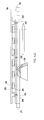
FIG. 3 is a cross-sectional elevational view of a subassembly being prepared using a subassembly fixture in accordance with the invention. -
FIG. 4 is a cross-sectional elevational view of a wave soldering step that may be used in accordance with the invention to complete the assembly. -
FIG. 4A is cross-sectional elevational view of an alternative embodiment in which the heat sink includes standoffs and fasteners to attach the heat sink directly to a printed circuit board. -
FIG. 5 is a histogram that is normalized to show the variation of thermal bondline thickness using a process of this invention, and using a conventional process. - The steps in a conventional process for assembling power packages and a thermal heat rail on a printed circuit board is illustrated schematically in
FIG. 1 . Thefirst step 10 involves procurement of a printed circuit board having appropriate printed circuitry for the power packages and appropriately located lead holes for the leads of the power packages, and procurement of the power packages and heat sink. Thereafter, astep 20 of applying plastic standoff spacers to the printed circuit board is performed. The plastic standoff spacers are intended to provide the correct spacing between the power packages and the circuit board. Next, the leads on the power packages are inserted into the corresponding lead holes in the printed circuit board instep 30. A clamp fixture instep 40 is used for holding the power packages against the plastic standoffs so that the power packages are held in place during asoldering operation 50. Thereafter, the subassemblies comprising the power packages soldered to the printed circuit board are removed from the fixture and a heat rail is affixed to the outer exposed surfaces of the power packages instep 60. - Unfortunately, the process described above and shown in
FIG. 1 results in differences among the height of the plurality of power packages mounted on the printed circuit board, and also results in individual power packages being tilted at an angle with respect to each other and with respect to the printed circuit board. As a result, in order to achieve excellent planar contact between the outer exposed surfaces of the power packages and a surface of the planar heat sink or heat rail, the leads on the power packages must be bent slightly. However, excessive bending (e.g., more than about 0.010 inch) can cause physical damage to the power package resulting in reduced quality and reduced reliability. - A process in accordance with the invention is illustrated schematically in
FIG. 2 .Procurement step 110 is substantially the same asprocurement step 10 ofFIG. 1 . The printed circuit board in accordance with the process of this invention is placed into a fixture duringstep 120 to immobilize the printed circuit board during subsequent operations. Next, instep 130, the electrical leads of the power packages are inserted into corresponding lead holes provided in the printed circuit board. Thermal interface adhesive material is then applied to the heat rail instep 140. Thereafter, instep 150, the outwardly facing surfaces of the power packages, opposite the surfaces facing toward the printed circuit board, are pressed against the adhesive material applied to the heat rail to secure the power packages to the heat rail. - With excellent planar heat rail surface to planar power package surface contact being provided while the leads are still loosely inserted in the printed circuit board, the subassembly is transferred, in
step 160, to a wave solder pallet and the leads of the power packages are wave soldered instep 170 to the printed circuit board. Finally, instep 180, the completed assembly is removed from a fixture used during the soldering step.
A suitable fixture for preparing a subassembly in which thepower packages 200 are attached to aheat rail 204 is shown inFIG. 3 . The expression "power packages" as used herein refers to an electrical or electronic component that generates a substantial amount of heat that must be, or at least is desirably, dissipated by a heat sink attached to the power packages. Examples of power packages include transistors such as a MOSFET (metal oxide semiconductor field effect transistor), IGBT (isolated gate bipolar transistor), diode, thyristor, etc. The fixture includes abase 207, anupper fixture member 205 andstandoffs 208.Circuit board 202 is positioned on circuit board supports 206 (located at each of the four corners of the printed circuit board). Theelectrical leads 201 of thepower packages 200 are inserted into the corresponding holes provided in the printedcircuit board 202. Thepower packages 200 may be affixed to thethermal heat sink 204 with a thermal interfaceadhesive material 203 that may be appropriately patterned onto the underside of a thermal heat sink 204 (e.g., an aluminum plate), the uppersurface power devices 200, or both the underside ofthermal heat sink 204 and the upper surface ofpower devices 200. - As an alternative to adhesively affixing an upper surface of the power packages to the printed circuit board, the power packages may be temporarily affixed to the heat sink using a mechanical clamp mechanism. After soldering is complete, the power devices may be held in intimate contact with the heat sink using a spring fixture similar to that described above and illustrated in
FIG. 3 . - Before and during assembly of the fixture (205, 207 and 208) around the subassembly,
power packages 200 are loosely held on printedcircuit board 202. A force may be applied to the underside of the powerpackages using springs 210 that act through plungers orpins 209 which extend upwardly fromspring 210 and through a plunger aperture provided through printedcircuit board 202. Thespring 210 may be an elastomeric member, a metal coil spring, a metal leaf spring or any other suitable means for urgingpower packages 200 against heat rail orheat sink 204. The fixture is used to achieve intimate planar surface to planar surface contact between thepower packages 200 and theheat sink 204. - After the power packages have been attached to the heat sink, the same fixture may be used for wave soldering the
leads 201 of thepower packages 200 as shown inFIG. 4 . During wave soldering, thebase portion 207 of the fixture is removed and the underside ofprinted circuit board 202 is moved in the direction shown byarrow 220 to pass the portions ofleads 201 extending throughcircuit board 202 through a schematically illustratedsolder wave 230. - As an alternative to using the upper fixture to hold the heat sink and power devices in place during soldering, a rigid heat sink may itself be used as a fixturing device as shown in
FIG. 4A . By including standoff features 250 on the heat sink, a fixed height above the circuit board can be established. Screws or othersuitable fasteners 260 may be used to attach the heat sink directly to the board. This method limits board movement during the solder process and provides additional structural strength to the final assembly. - Employing a process of this invention using an adhesive to bond the power packages 200 to the
thermal heat sink 204, it was found that very uniform bondline thicknesses (the thickness of the adhesive layer between the power packages and the thermal heat sink) could be achieved. -
FIG. 5 shows a comparison of the bondline thicknesses achieved using an assembly process of the invention with the bondline thicknesses achieved when a conventional process is used to assemble the same components. The histogram ofFIG. 5 shows that all measured bondline thicknesses were well within a targeted or required tolerance (± 64 microns), whereas the conventional process produced a high rate (frequency) of measurements that were well outside of the targeted or required variance. - It will be understood by those who practice the invention and those skilled in the art that various modifications and improvements may be made to the invention without departing from the spirit of the disclosed concept. The scope of protection afforded is to be determined by the claims and by the breadth of interpretation allowed by law.
Claims (10)
- A process for assembling a printed circuit board, a plurality of power packages and a thermal heat sink, comprising steps of:providing a plurality of power packages having electrical leads;providing a printed circuit board having printed circuitry and lead holes for the power packages;inserting the electrical leads of the power packages into the lead holes of the printed circuit board;affixing an upper surface of each of the power packages to a thermal heat sink; andsoldering the electrical leads of the plurality of power packages to the printed circuit board.
- The process of claim 1, wherein the plurality of power packages are attached to the heat sink and positioned on the printed circuit board by steps of:placing the printed circuit board into a fixture that holds the printed circuit board in a fixed position and orientation;positioning the plurality of power packages onto the printed circuit board with the leads of the power packages extending into corresponding lead holes of the printed circuit board;applying a thermal interface adhesive material to an underside of a heat sink;holding the underside of the heat sink against outwardly facing surfaces of the power packages; andexerting a force against the side of each of the power packages opposite the outwardly facing side to urge the outwardly facing surfaces of the power packages against the heat sink.
- The process of claim 2, wherein the forces applied to the power packages are applied through a plunger projecting through an opening in the printed circuit board.
- The process of claim 2, wherein the force exerted against the power packages to urge the power packages against the heat sink is provided by springs attached to the fixture.
- The process of claim 4, wherein the springs are elastomeric members.
- The process of claim 4, wherein the springs are metal coil springs or leaf springs.
- The process of claim 1, wherein the thermal heat sink is an aluminum plate.
- The process of claim 1, wherein the step of soldering comprising moving an underside of the printed circuit board toward a solder wave to pass portions of electrical leads extending from power packages above the printed circuit board and projecting downwardly from the underside of the circuit board through the solder wave.
- The process of claim 1, wherein the step of affixing an upper surface of each of the power packages to a thermal heat sink includes applying an adhesive to at least one of the upper surfaces of the power packages and the underside of the thermal heat sink, and urging the upper surfaces of the power packages against the underside of the thermal heat sink.
- The process of claim 1, wherein the step of affixing an upper surface of each of the power packages to a thermal heat sink includes mechanically clamping the power packages on the thermal heat sink.
Applications Claiming Priority (1)
| Application Number | Priority Date | Filing Date | Title |
|---|---|---|---|
| US11/818,840 US20080307643A1 (en) | 2007-06-15 | 2007-06-15 | Method of assembly to achieve thermal bondline with minimal lead bending |
Publications (2)
| Publication Number | Publication Date |
|---|---|
| EP2003942A2 true EP2003942A2 (en) | 2008-12-17 |
| EP2003942A3 EP2003942A3 (en) | 2009-11-18 |
Family
ID=39731509
Family Applications (1)
| Application Number | Title | Priority Date | Filing Date |
|---|---|---|---|
| EP08156905A Withdrawn EP2003942A3 (en) | 2007-06-15 | 2008-05-26 | Method of assembly to achieve thermal bondline with minimal lead bending |
Country Status (2)
| Country | Link |
|---|---|
| US (1) | US20080307643A1 (en) |
| EP (1) | EP2003942A3 (en) |
Cited By (2)
| Publication number | Priority date | Publication date | Assignee | Title |
|---|---|---|---|---|
| DE102010003294A1 (en) * | 2010-03-25 | 2011-09-29 | Deutsches Zentrum für Luft- und Raumfahrt e.V. | Manufacturing electrically conductive composite material, comprises applying functional layer on electrically conductive support material by spraying or rolling, and supplying electric field such as direct current to the functional layer |
| WO2012084556A1 (en) * | 2010-12-22 | 2012-06-28 | Epcos Ag | Electrical module for being received by automatic placement machines by means of generating a vacuum |
Families Citing this family (6)
| Publication number | Priority date | Publication date | Assignee | Title |
|---|---|---|---|---|
| ITMI20112084A1 (en) * | 2011-11-17 | 2013-05-18 | St Microelectronics Srl | WAVE WELDING ON PRINTED CIRCUIT BOARD OF SURFACE MOUNTED ELECTRONIC DEVICES |
| US9148962B2 (en) * | 2013-01-02 | 2015-09-29 | International Business Machines Corporation | Heat transfer device for wave soldering |
| ITMI20130520A1 (en) * | 2013-04-05 | 2014-10-06 | St Microelectronics Srl | CONSTRUCTION OF A HEAT SINK THROUGH WELDING |
| US10965079B2 (en) * | 2018-10-26 | 2021-03-30 | Schweitzer Engineering Laboratories, Inc. | Comb pattern insert for wave solder pallets |
| US11886177B1 (en) | 2022-08-26 | 2024-01-30 | Arch Systems Inc. | System and method for manufacturing system data analysis |
| US11947340B1 (en) | 2022-08-26 | 2024-04-02 | Arch Systems Inc. | System and method for machine program analysis |
Family Cites Families (11)
| Publication number | Priority date | Publication date | Assignee | Title |
|---|---|---|---|---|
| US5305185A (en) * | 1992-09-30 | 1994-04-19 | Samarov Victor M | Coplanar heatsink and electronics assembly |
| MY112145A (en) * | 1994-07-11 | 2001-04-30 | Ibm | Direct attachment of heat sink attached directly to flip chip using flexible epoxy |
| US5581443A (en) * | 1994-09-14 | 1996-12-03 | Kabushiki Kaisha Toshiba | Structure for cooling a circuit module having a circuit board and a heat-generating IC chip mounted on the board, and portable electronic apparatus incorporating the structure |
| US5820013A (en) * | 1996-07-01 | 1998-10-13 | Innovative Soldering Technologies | Adjustable support apparatus for wave soldering of printed circuit boards |
| US5978223A (en) * | 1998-02-09 | 1999-11-02 | International Business Machines Corporation | Dual heat sink assembly for cooling multiple electronic modules |
| US6255722B1 (en) * | 1998-06-11 | 2001-07-03 | International Rectifier Corp. | High current capacity semiconductor device housing |
| US6203191B1 (en) * | 1998-10-28 | 2001-03-20 | Speculative Incorporated | Method of junction temperature determination and control utilizing heat flow |
| US6831838B1 (en) * | 2003-05-14 | 2004-12-14 | Illinois Tool Works Inc. | Circuit board assembly for welding power supply |
| JP3102658U (en) * | 2004-01-05 | 2004-07-15 | 船井電機株式会社 | heatsink |
| US20050264998A1 (en) * | 2004-05-25 | 2005-12-01 | 3M Innovative Properties Company | Heat sink assembly |
| US7324342B2 (en) * | 2005-10-19 | 2008-01-29 | Delphi Technologies, Inc. | Electronics assembly and electronics package carrier therefor |
-
2007
- 2007-06-15 US US11/818,840 patent/US20080307643A1/en not_active Abandoned
-
2008
- 2008-05-26 EP EP08156905A patent/EP2003942A3/en not_active Withdrawn
Cited By (2)
| Publication number | Priority date | Publication date | Assignee | Title |
|---|---|---|---|---|
| DE102010003294A1 (en) * | 2010-03-25 | 2011-09-29 | Deutsches Zentrum für Luft- und Raumfahrt e.V. | Manufacturing electrically conductive composite material, comprises applying functional layer on electrically conductive support material by spraying or rolling, and supplying electric field such as direct current to the functional layer |
| WO2012084556A1 (en) * | 2010-12-22 | 2012-06-28 | Epcos Ag | Electrical module for being received by automatic placement machines by means of generating a vacuum |
Also Published As
| Publication number | Publication date |
|---|---|
| US20080307643A1 (en) | 2008-12-18 |
| EP2003942A3 (en) | 2009-11-18 |
Similar Documents
| Publication | Publication Date | Title |
|---|---|---|
| EP2003942A2 (en) | Method of assembly to achieve thermal bondline with minimal lead bending | |
| US5175410A (en) | IC package hold-down fixture | |
| US6544864B2 (en) | Methods employing hybrid adhesive materials to secure components of semiconductor device assemblies and packages to one another and assemblies and packages including components secured to one another with such hybrid adhesive materials | |
| US3650454A (en) | Device for bonding with a compliant medium | |
| CN101111932A (en) | Mounting device for electrical components | |
| US20020019153A1 (en) | Connecting devices and method for interconnecting circuit components | |
| IL30276A (en) | Bonding with a compliant medium | |
| JP3699575B2 (en) | IC package mounting method | |
| US3669333A (en) | Bonding with a compliant medium | |
| JPH0320051A (en) | Semiconductor device mounting structure and mounting method and mounting device | |
| CN109315067A (en) | Transfer method and installation method | |
| JPH1167795A (en) | Semiconductor chip mounting apparatus, semiconductor chip mounting method, and semiconductor device | |
| JP3620399B2 (en) | Manufacturing method of electrical equipment | |
| JP2001308146A (en) | Apparatus for mounting semiconductor chips on chip carriers | |
| JPH05243439A (en) | Heat sink mounting mechanism | |
| JPH10173007A (en) | Bare chip mounting device | |
| JP6619121B1 (en) | Semiconductor device manufacturing method, semiconductor device manufacturing jig, and semiconductor device | |
| JPH07154065A (en) | Printed circuit board straightening jig | |
| JP3348830B2 (en) | Solder bump bonding apparatus and solder bump bonding method | |
| JPH087651Y2 (en) | Electronic component holding structure | |
| JP3001483B2 (en) | Lead frame, semiconductor device and method of manufacturing the same | |
| CN111146096B (en) | Double-sided heat dissipation semiconductor device and single-reflow soldering method thereof | |
| KR0185304B1 (en) | Apparatus for Mounting TPC Integrated Circuits and Method for Mounting CFPC Integrated Circuits | |
| JPH0539630Y2 (en) | ||
| JP3091039B2 (en) | Transistor mounting method and transistor mounting guide |
Legal Events
| Date | Code | Title | Description |
|---|---|---|---|
| PUAI | Public reference made under article 153(3) epc to a published international application that has entered the european phase |
Free format text: ORIGINAL CODE: 0009012 |
|
| AK | Designated contracting states |
Kind code of ref document: A2 Designated state(s): AT BE BG CH CY CZ DE DK EE ES FI FR GB GR HR HU IE IS IT LI LT LU LV MC MT NL NO PL PT RO SE SI SK TR |
|
| AX | Request for extension of the european patent |
Extension state: AL BA MK RS |
|
| PUAL | Search report despatched |
Free format text: ORIGINAL CODE: 0009013 |
|
| AK | Designated contracting states |
Kind code of ref document: A3 Designated state(s): AT BE BG CH CY CZ DE DK EE ES FI FR GB GR HR HU IE IS IT LI LT LU LV MC MT NL NO PL PT RO SE SI SK TR |
|
| AX | Request for extension of the european patent |
Extension state: AL BA MK RS |
|
| AKX | Designation fees paid | ||
| REG | Reference to a national code |
Ref country code: DE Ref legal event code: 8566 |
|
| STAA | Information on the status of an ep patent application or granted ep patent |
Free format text: STATUS: THE APPLICATION IS DEEMED TO BE WITHDRAWN |
|
| 18D | Application deemed to be withdrawn |
Effective date: 20100519 |