EP2002273B1 - Electric potential sensor - Google Patents
Electric potential sensor Download PDFInfo
- Publication number
- EP2002273B1 EP2002273B1 EP07712718.1A EP07712718A EP2002273B1 EP 2002273 B1 EP2002273 B1 EP 2002273B1 EP 07712718 A EP07712718 A EP 07712718A EP 2002273 B1 EP2002273 B1 EP 2002273B1
- Authority
- EP
- European Patent Office
- Prior art keywords
- amplifier
- sensor
- circuit
- input
- electric potential
- Prior art date
- Legal status (The legal status is an assumption and is not a legal conclusion. Google has not performed a legal analysis and makes no representation as to the accuracy of the status listed.)
- Active
Links
Images



Classifications
-
- G—PHYSICS
- G01—MEASURING; TESTING
- G01R—MEASURING ELECTRIC VARIABLES; MEASURING MAGNETIC VARIABLES
- G01R19/00—Arrangements for measuring currents or voltages or for indicating presence or sign thereof
- G01R19/0023—Measuring currents or voltages from sources with high internal resistance by means of measuring circuits with high input impedance, e.g. OP-amplifiers
-
- A—HUMAN NECESSITIES
- A61—MEDICAL OR VETERINARY SCIENCE; HYGIENE
- A61B—DIAGNOSIS; SURGERY; IDENTIFICATION
- A61B5/00—Measuring for diagnostic purposes; Identification of persons
- A61B5/24—Detecting, measuring or recording bioelectric or biomagnetic signals of the body or parts thereof
- A61B5/25—Bioelectric electrodes therefor
- A61B5/277—Capacitive electrodes
-
- G—PHYSICS
- G01—MEASURING; TESTING
- G01R—MEASURING ELECTRIC VARIABLES; MEASURING MAGNETIC VARIABLES
- G01R29/00—Arrangements for measuring or indicating electric quantities not covered by groups G01R19/00 - G01R27/00
- G01R29/12—Measuring electrostatic fields or voltage-potential
Definitions
- the present invention concerns electric potential sensors for use for the measurement of potentials non-invasively in a wide variety of applications, for example in the fields of medical diagnostics and biometric sensing.
- an electrodynamic sensor in which different circuit techniques are combined to achieve several orders of magnitude improvement in sensitivity, by comparison with previously known electrodynamic sensors, whilst still maintaining sufficient stability to permit a relatively unskilled operator to make measurements in everyday conditions.
- an electrodynamic sensor is provided, which comprises a high input impedance electrometer adapted to measure small electrical potentials originating from an object under test by means of at least one input probe, which has no direct electrical contact with the object.
- the circuit arrangement of the electrometer of this invention comprises an amplifier which includes a combination of ancillary circuits arranged cumulatively to increase the sensitivity of said electrometer to said small electrical potentials whilst not perturbing the electrical field associated therewith, the ancillary circuits serving to provide at least two of guarding, bootstrapping, neutralisation, supply rail drift correction, supply modulation and offset correction for said sensor.
- the capacitive coupling to the sample may be comparable with or much smaller than the input capacitance of the sensor.
- the measurement signal received by the sensor is attenuated by the capacitive potential divider formed by the coupling capacitance and the input capacitance and may be difficult to capture.
- Lanyi discusses an analysis of the noise of input stages comprising a high-input-impedance buffer and a current-to-voltage converter operated with high-impedance sources. He indicates that the noise may at first sight achieve unexpectedly high values, and concludes that in the case of the buffer the bootstrap of a biasing circuit, which is applied to increase the input impedance, multiplies the dominant thermal noise of the biasing resistor.
- the present invention seeks to overcome the problems described above and to provide a novel electric potential sensor which is capable of highly accurate and non-invasive signal measurement.
- the present invention also seeks to provide an electric potential sensor in which the signal to noise ratio is significantly enhanced.
- the present invention further seeks to provide various techniques and combinations of techniques for enhancing the signal to noise ratio in an electric potential sensor.
- an electric potential sensor according to claim 1.
- such a electric potential sensor comprises: at least one detection electrode arranged for capacitive coupling with a sample under test and for generating a measurement signal; a sensor amplifier adapted to receive the measurement signal as input and to supply an amplified detection signal as output; input impedance enhancing means including a bootstrapping circuit for providing a high input impedance to the electric potential sensor for increasing the sensitivity of the electrode to reduced electric potentials; and a discrete pre-amplifier stage inserted between the detection electrode and the sensor amplifier so as to reduce the input capacitance of the electric potential sensor.
- the discrete pre-amplifier stage serves to increase the amplitude of the input measurement signal and thereby to increase the signal to noise ratio and enhance signal measurement.
- the discrete pre-amplifier stage may, for example, be provided by a high electron mobility transistor, or a FET arrangement.
- the input impedance enhancing means may comprise a guard circuit, the bootstrapping circuit and a neutralisation circuit.
- the input impedance enhancing means may also further comprise one or more circuits for supply rail drift correction, supply modulation and offset correction for the sensor.
- the detection electrode is juxtaposed with a conducting element connected to a zero reference potential in order to reduce effective source impedance, the conducting element being in the form of an annular ring surrounding the detection electrode.
- such means for reducing the noise amplitude may comprise at least one of a dc stability gain setting circuit, a noise matching circuit, and an enhanced bootstrap circuit.
- the present invention thus aims to increase the signal to noise ratio either by increasing the amplitude of the signal or by decreasing the amplitude of the noise or both.
- an eletrodynamic sensor 10 according International Patent Application number WO 03/048789 comprises a detection electrode 12 connected to the non-inverting input of a sensor amplifier 14.
- the detection electrode 12 supplies a measurement signal to the sensor amplifier 14, whose output supplies an amplified detection signal as output.
- the detection electrode 12 includes an electrode disc 16 mounted on a conductive stem 18, the electrode disc 16 comprising a surface oxide layer 20 on a substrate 22.
- the sensor amplifier 14 has a fixed input resistance 24, connected between the electrode 12 and the non-inverting input of the amplifier 14, to provide a steady input bias current to the amplifier 14.
- the input resistor 24 will generally have a high resistance of the order of 100 G ⁇ s or greater.
- the sensor amplifier 14 also has a guard 26 physically surrounding the input circuitry including the electrode 12 and the resistor 24 and providing a shield driven by the output of the amplifier 14. Stray capacitance is thus alleviated by means of this positive feedback technique by maintaining the same potential on the guard or shield 26 as on the input detection electrode 12.
- circuit components may be provided for bootstrapping and neutralisation of the sensor as described in International Patent Application number WO 03/048789 .
- the earlier sensor shown in Figure 1 may be employed as a sensor probe for electrodynamic body sensing to obtain biometric measurements either in a contact mode, in which case the oxide layer 20 forms a capacitor providing relatively strong electrical coupling to the skin of a person under observation, or in an electrically isolated sensing mode, in which case the oxide layer 20 may be omitted and capacitive couple providing a relatively weak electrical coupling may be achieved through clothing or other intervening layers.
- a sensor 28 according to the present invention will now be described with reference to Figure 2 , such sensor effectively comprising the sensor 10 of Figure 1 , with its detection electrode 12 and sensor amplifier 14, but with the inclusion of further and different components to increase the accuracy of signal measurement, particularly in cases where a weak capacitive coupling to the subject under test is present.
- One such additional component comprises an annular conducting element 12a surrounding the electrode 12 and connected to a reference voltage potential V r , such as earth or a zero potential point on the sensor amplifier 14.
- V r a reference voltage potential
- the effect of the annular element 12a is to reduce the source impedance, ie the coupling impedance between the sample under test and the input of the electric potential sensor 14 as provided by a combination of coupling resistance R c and coupling capacitance C c , by reducing the effective distance from the electrode 12 to the earthing point for the sensor amplifier 14.
- the element 12a does not need to be annular but may have other configurations.
- the sensor 28 of the present invention employs a discrete pre-amplifier stage 30, having an intrinsically lower device input capacitance than is available in commercial operational amplifiers, in conjunction with the features of the sensor 10 of Figure 1 .
- a discrete pre-amplifier stage 30 is shown diagrammatically in Figure 2 , and arrangements of this discrete device are described with reference to Figures 3 to 6 .
- the invention may also employ various bootstrapping techniques in conjunction with the pre-amplifier stage 30 in order to enhance the operation of the discrete device, as shown for example respectively in Figures 2 to 6 .
- the invention may employ techniques for reducing the amplitude of the noise, as shown for example in Figures 2 and 7 to 9 .
- FIG. 2 is a block diagram of the sensor 28 according to the invention illustrating how these different techniques may be applied to the sensor to enhance significantly the signal to noise ratio.
- the discrete pre-amplifier stage 30 of Figure 5 may be further enhanced by means of additional bootstrapping, for example provided by a cascode circuit connection 36 as shown in Figure 6 to bootstrap the source of a FET employed as the pre-amplifier stage 30, and/or provided by a drain bootstrap circuit 38 as shown in Figure 7 to bootstrap the drain of the FET.
- additional bootstrapping for example provided by a cascode circuit connection 36 as shown in Figure 6 to bootstrap the source of a FET employed as the pre-amplifier stage 30, and/or provided by a drain bootstrap circuit 38 as shown in Figure 7 to bootstrap the drain of the FET.
- FIG. 8 Further techniques for noise reduction, illustrated in Figures 8 to 12 , may also be applied to the sensor 28. Such techniques may include the provision of a dc stability gain setting circuit 40 shown in Figure 8 for overcoming the problem of low frequency instability, and/or of a noise matching circuit 42 shown in Figures 9 and 10 for addressing the problem of low frequency noise, and/or of an enhanced bootstrap circuit 44 shown in Figures 11 and 12 for addressing the problem of drift reduction. These additional circuits are all applicable to the versions of the sensor 28 including a discrete pre-amplifier stage 30 as described in relation to Figure 2 .
- the maximum signal to noise ratio will be obtained by utilising both a discrete pre-amplifier stage 30, as described below with reference to Figures 2 to 7 , and at least one of the techniques as described below in relation to Figures 8 to 12 .
- the available measurement signal is attenuated by a capacitive potential divider made up of the capacitances C c and C in . This is the case in practice for many remote monitoring applications and for microscopic probes, particularly for example in the field of biometric sensing. In this situation, the best way of increasing the signal to noise ratio would be to reduce the input capacitance C in to be less than or comparable with the coupling capacitance C c .
- commercially available operational amplifiers typically have input capacitances C in ranging from 1-10pF, and these cannot be reduced further.
- the present invention is based on the realisation that a discrete pre-amplifier stage 30 having an input capacitance as low as 0.1pF may be employed in conjunction with the detection electrode 12 and sensor amplifier 14 effectively to achieve a lower input capacitance.
- a discrete pre-amplifier stage 30 having an input capacitance as low as 0.1pF may be employed in conjunction with the detection electrode 12 and sensor amplifier 14 effectively to achieve a lower input capacitance.
- the use of such a device as a front end pre-amplifier will increase the available signal by a large factor (x10-x100).
- the pre-amplifier stage 30 is achieved using a high electron mobility transistor (HEMT) device 50 situated between the detection electrode 12 of the known sensor, represented in Figure 3 by an input V in , and the operational amplifier 14 of the known sensor.
- the HEMT device 50 displays very low noise characteristics due to the extremely high mobility of the charge carriers in the semiconducting channel of the device.
- the HEMT device 50 is configured in this instance as a common source amplifier, with the property of inverting voltage gain.
- a resistor Rd limits the current flowing through the channel of the HEMT device 50, and the DC operating point is set by the voltage applied to a gate resistor Rg connected to the gate of the HEMT device 50.
- the output signal taken from the drain of the HEMT device 50, is amplified by an operational amplifier OPA1, constituting the sensor amplifier 14, with the gain of the operational amplifier OPA1 set by a feedback connection of two resistors R1, R2 and a capacitor C1.
- An attenuated version of the output from the operational amplifier OPA1 is fed back and amplified by way of a positive feedback loop including the bootstrap circuit 32 (see Figure 2 ) comprising a further operational amplifier OPA2 arranged to provide a bootstrap signal via a capacitor C2 for the gate resistor Rg, thereby increasing the input impedance of the sensor 28.
- the gain of the operational amplifier OPA2 is set by two resistors R3 and R4.
- a resistor R5 provides a DC path for the input bias current required by the HEMT device 50.
- FIG. 4 Further enhancement of the signal to noise ratio may also be achieved by physically separating the first stage transistor 50, providing the pre-amplifier stage 30, from the following electronics and operating at a reduced temperature, for example as shown in Figure 4 .
- the circuit of Figure 4 is similar to that of Figure 3 , with the exception that the portion of the circuit to the left of the dashed line is maintained at cryogenic temperatures for reduced temperature operation and the portion to the right is at room temperature.
- the HEMT device 50 may take the form either of a pre-amplifier in front of the sensor amplifier 14, as shown in Figures 3 and 4 . Further, the HEMT device 50 may comprise two or more devices if used differentially.
- a silicon dual gate MOSFET 60 (or two FETs so connected) is employed as the pre-amplifier stage 30.
- the MOSFET 60 is biased by means of an appropriate drain resistor R d to give an inverting voltage gain.
- the input signal from the sensor electrode 12 is coupled to gate G2 of the MOSFET 60, with gate G1 of the MOSFET 60 being held at an appropriate bias voltage by means of a further resistor R G1 .
- An input bias current in this example is provided by a high value resistor R b , typically having a resistance in the range 10 - 100 G ⁇ , to which is connected the bootstrap circuit 32, here comprising a parallel connection of a capacitor C4 and resistor R10 providing the necessary coupling and DC bias to the resistor R b .
- the output of the MOSFET 60 in this arrangement contains both the amplified input signal and an unwanted DC offset.
- This DC offset may be removed by means of the DC level restoring circuit 34 in conjunction with the following operational amplifier circuit OPA3, which is configured as a differential amplifier and which represents the sensor amplifier 14 of the sensor 28.
- the gain of the operational amplifier OPA3 is set by resistors R6 and R8 for its inverting input and by resistors R7 and R9 for its non-inverting input.
- a capacitor C3 is connected across the resistor R9, so as to act as a low pass filter which rejects the AC component of the signal coupled to it, thereby leaving the DC offset.
- the difference signal which is amplified by the operational amplifier OPA3, consists only of the wanted signal.
- This technique has the advantage that it responds to any DC drift present in the output of the MOSFET 60 and removes this from the signal below a corner frequency set by the time constant of the filter components.
- the output from the operational amplifier OPA3 is suitable to provide a positive feedback signal for the guard circuit as shown in Figure 1 and the bootstrap circuit 32 as already described, as well as a neutralisation circuit as described in International Patent Application No. WO 03/048789 .
- An input capacitance ⁇ 1pF for the sensor 28 with the configuration of Figure 5 has been measured in experimental trials using this arrangement.
- the DC input bias current described above as being provided by the resistor R b may in practice be provided by one or a combination of three means: First, by leakage through the bootstrap capacitor C4 (usually the effective resistance of the capacitor is much lower than the resistance of the bias resistor); second, by the addition of the resistor R10 in parallel with the bootstrap capacitor C4; and third, by including a resistor to ground from the junction of the bias resistor R b and the bootstrap capacitor C4.
- the silicon dual gate MOSFET 60 is connected in a cascode configuration where the device is internally bootstrapped to the source S so that internal bootstrapping is provided within the pre-amplifier stage.
- cascode connection 36 (see Figure 2 ) has the effect of greatly reducing the input capacitance C in both of the MOSFET 60 and, since the MOSFET 60 is the input stage of the sensor 28, of the overall sensor.
- the voltage gain of the first discrete pre-amplifier stage provided by the MOSFET 60 is unity and non-inverting.
- the output of the MOSFET 60 is again fed through the DC level restorer circuit 34 including the operational amplifier OPA3 (amplifier 14) and is then coupled to an inverting amplifier OPA4 to provide the correct phase of feedback signal for the bootstrap circuit 32.
- the gain of the operational amplifier OPA4 is set by two resistors R11 and R12. A fraction of the output from the operational amplifier OPA4 is used for the bootstrap circuit 32 as before.
- An input capacitance ⁇ 0.2pF has been measured in experimental trials using this configuration for the sensor 28.
- FIG. 7 A further enhancement of the Figure 6 arrangement with the cascode circuit connection 36 is possible as shown in the arrangement of Figure 7 .
- an additional bootstrap 38 to the drain D of the MOSFET 60 as well as the bootstrap to the source S enables the intrinsic input capacitance to be further reduced.
- This additional bootstrap 38 is achieved in this instance using a bootstrap capacitor C5 connected between the MOSFET end of the parallel connection of the capacitor C4 and resistor R10 and the drain D of the MOSFET 60. It is alternatively possible to employ an independently derived bootstrap signal obtained e.g. from the other end of the parallel connection of C4/R10.
- the input capacitance may be reduced to ⁇ 0.1pF using the circuit of Figure 7 .
- the signal would remain measurable, with a 10:1 1 signal to noise ratio, for coupling capacitances down to ⁇ 10 -15 F, assuming a 1 volt signal at the source.
- the effect of this is to reduce the gain of the sensor amplifier 14 to unity at DC whilst maintaining a high gain at the signal frequencies, hence stabilising the sensor and improving the settling time. Hence, it is possible to achieve low noise performance with high voltage gain and stability.
- the noise performance of a differential input amplifier depends on many factors. Amongst the parameters to be considered are the level of the source impedance, ie the coupling impedance between the sample under test and the input of the sensor amplifier 14 as provided by a combination of coupling resistance R c and coupling capacitance C c , compared to the input impedance, provided by a combination of input resistance R in and input capacitance C in for the amplifier 14, and the extent to which the relative contributions of the voltage and current noise combine to create overall frequency dependent noise as observed at the output of the amplifier 14. For a situation in which the coupling impedance between the sample and the input is very high (i.e. R c >>R in and/or C c ⁇ C in ), this factor may have a very large effect on the frequency dependent noise.
- Close impedance matching between the inverting and non-inverting inputs of the sensor amplifier 14 serves not only to maximise the common mode rejection ratio, but also to minimise the noise.
- This may be achieved by the inclusion of a frequency dependent matching network, for example as shown in Figure 9 , providing the noise matching circuit 42 of Figure 2 .
- the parallel components R m , C m could be replaced by a parallel combination of a FET and a varactor diode, with suitable biasing components, as shown in Figure 10 , to allow remotely tunable values for the resistance and capacitance for signal to noise optimisation.
- Bias voltages V g and V v control the resistance of the FET channel and the capacitance of the varactor diode respectively.
- the noise matching circuit 42 of Figures 9 or 10 may advantageously be employed in combination with one or more of the techniques described with reference to the arrangements of Figures 3 to 7 .
- the bootstrap signal must then be precisely x1 if maximum bootstrap and stable operation is to be achieved.
- the output signal from the amplifier 14 is fed back through the bootstrap capacitor C to a 1/10 resistive attenuator, comprising further resistors R and 9R in a 9:1 ratio, shown on the left hand side of the capacitor C in Figure 11 , to provide the x1 bootstrap signal.
- a variation on the enhanced bootstrap circuit 44 of Figure 11 uses a high pass filter to set the lower operating frequency of the bootstrap circuit as shown in Figure 12 .
- the time constant is set by two resistor-capacitor pairs (RC) connected in the feedback circuit from the output of the amplifier 14, which RC pairs, together with a high impedance buffer amplifier OPA6, form a second order high pass filter.
- the gain is provided by two gain setting resistors R1 and R2.
- variation of Figure 12 may employ either a passive high pass filter followed by a high impedance buffer amplifier or an active high pass filter, both of which enable low frequency operation to be achieved with convenient values of R and C.
- the enhanced bootstrap circuit 44 may advantageously be employed in combination with one or more of the techniques described with reference to the arrangements of Figures 3 to 7 .
- circuits described with reference to Figures 8 to 12 may be employed individually or in combination with the techniques described with reference to the arrangements of Figures 3 to 7 .
Landscapes
- Physics & Mathematics (AREA)
- Health & Medical Sciences (AREA)
- Life Sciences & Earth Sciences (AREA)
- General Physics & Mathematics (AREA)
- Medical Informatics (AREA)
- Engineering & Computer Science (AREA)
- Biomedical Technology (AREA)
- Heart & Thoracic Surgery (AREA)
- Pathology (AREA)
- Molecular Biology (AREA)
- Surgery (AREA)
- Animal Behavior & Ethology (AREA)
- General Health & Medical Sciences (AREA)
- Public Health (AREA)
- Veterinary Medicine (AREA)
- Biophysics (AREA)
- Amplifiers (AREA)
Description
- The present invention concerns electric potential sensors for use for the measurement of potentials non-invasively in a wide variety of applications, for example in the fields of medical diagnostics and biometric sensing.
- In order to create a sensitive electrodynamic measuring device, it is customary to provide a high input impedance and thereby reduce the power of the input signal required to operate the device. However, electronic circuits with a very high input impedance tend to be unstable, and so practical devices are usually a compromise between achieving the necessary degree of sensitivity, providing the desired input impedance and ensuring an acceptable degree of stability.
- In International Patent Application No.
WO 03/048789 - Whilst these features assist in providing a sensor with high input impedance and a relatively stable operation, nevertheless, in situations where there may be weak capacitive coupling to, or a signal of small amplitude generated by, a source or sample under test, noise problems may still remain and may inhibit or prevent accurate signal measurement. This is particularly the case in certain medical and microscopic applications in which there is only a weak capacitive coupling and yet highly accurate signal measurement is essential, for example in a remote off-body mode of sensing in which the or each probe has no physical contact with the human body and typically the weak capacitive coupling would be <1pF.
- More particularly, in applications where there is a weak coupling between a sample under test and the sensor electrode, the capacitive coupling to the sample may be comparable with or much smaller than the input capacitance of the sensor. In this case, the measurement signal received by the sensor is attenuated by the capacitive potential divider formed by the coupling capacitance and the input capacitance and may be difficult to capture.
- In a paper entitled "The Noise of Input Stages with Low Parasitic Capacitance", published in Measurement Science and Technology 12 (2001) 1456-1464, Lanyi discusses an analysis of the noise of input stages comprising a high-input-impedance buffer and a current-to-voltage converter operated with high-impedance sources. He indicates that the noise may at first sight achieve unexpectedly high values, and concludes that in the case of the buffer the bootstrap of a biasing circuit, which is applied to increase the input impedance, multiplies the dominant thermal noise of the biasing resistor.
- There is thus a significant need for an electric potential sensor in which the possibility for accurate signal measurement is enhanced in cases of weak capacitive coupling to a sample under test.
- Such a need is especially pronounced in cases where accuracy of signal measurement is crucial, for example in cases of biometric and medical measurement.
- There is also a significant need for an electric potential sensor in which the signal to noise ratio is substantially improved.
- The present invention seeks to overcome the problems described above and to provide a novel electric potential sensor which is capable of highly accurate and non-invasive signal measurement.
- The present invention also seeks to provide an electric potential sensor in which the signal to noise ratio is significantly enhanced.
- The present invention further seeks to provide various techniques and combinations of techniques for enhancing the signal to noise ratio in an electric potential sensor.
- According to the invention, there is provided an electric potential sensor according to
claim 1. - As described, such a electric potential sensor comprises: at least one detection electrode arranged for capacitive coupling with a sample under test and for generating a measurement signal; a sensor amplifier adapted to receive the measurement signal as input and to supply an amplified detection signal as output; input impedance enhancing means including a bootstrapping circuit for providing a high input impedance to the electric potential sensor for increasing the sensitivity of the electrode to reduced electric potentials; and a discrete pre-amplifier stage inserted between the detection electrode and the sensor amplifier so as to reduce the input capacitance of the electric potential sensor.
- According to the invention, the discrete pre-amplifier stage serves to increase the amplitude of the input measurement signal and thereby to increase the signal to noise ratio and enhance signal measurement. The discrete pre-amplifier stage may, for example, be provided by a high electron mobility transistor, or a FET arrangement.
- The input impedance enhancing means may comprise a guard circuit, the bootstrapping circuit and a neutralisation circuit. The input impedance enhancing means may also further comprise one or more circuits for supply rail drift correction, supply modulation and offset correction for the sensor.
- In a preferred embodiment described below, the detection electrode is juxtaposed with a conducting element connected to a zero reference potential in order to reduce effective source impedance, the conducting element being in the form of an annular ring surrounding the detection electrode.
- In a further embodiment of the invention, there is provided in addition means for reducing the noise amplitude in order to increase the signal to noise ratio. For example, such means for reducing the noise amplitude may comprise at least one of a dc stability gain setting circuit, a noise matching circuit, and an enhanced bootstrap circuit.
- The present invention thus aims to increase the signal to noise ratio either by increasing the amplitude of the signal or by decreasing the amplitude of the noise or both.
- The present invention will now be described further, by way of example, with reference to the accompanying drawings, in which:
-
Figure 1 is a circuit diagram of an electrodynamic sensor according to the prior art; -
Figure 2 is a block diagram of an electrodynamic sensor according to the present invention; -
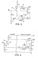
Figure 3 is a circuit diagram of a discrete pre-amplifier stage employed in the sensor ofFigure 2 , with bootstrapping; -
Figure 4 is a circuit diagram of a modification of theFigure 3 circuit; -
Figure 5 is a circuit diagram of a of discrete pre-amplifier stage provided by a FET, with bootstrapping and a DC level restorer circuit; -
Figure 6 is a circuit diagram of a modification of theFigure 5 circuit having a cascode circuit for bootstrapping the source of the FET; -
Figure 7 is a circuit diagram of a further modification of theFigure 5 circuit having a drain bootstrapping circuit for bootstrapping the drain of the FET; -
Figure 8 is a circuit diagram of a DC stability gain setting circuit shown inFigure 2 ; -
Figure 9 is a circuit diagram of a noise matching circuit shown inFigure 2 ; -
Figure 10 is a circuit diagram of a modification of the noise matching circuit ofFigure 9 ; -
Figure 11 is a circuit diagram of an enhanced bootstrapping circuit shown inFigure 2 ; and -
Figure 12 is a circuit diagram of a modification of the enhanced bootstrapping circuit ofFigure 11 . - Referring to
Figure 1 , an electrodynamic sensor as disclosed in International Patent Application No.WO 03/048789 - As shown in
Figure 1 , aneletrodynamic sensor 10 according International Patent Application numberWO 03/048789 detection electrode 12 connected to the non-inverting input of asensor amplifier 14. In use, thedetection electrode 12 supplies a measurement signal to thesensor amplifier 14, whose output supplies an amplified detection signal as output. - The
detection electrode 12 includes anelectrode disc 16 mounted on aconductive stem 18, theelectrode disc 16 comprising asurface oxide layer 20 on asubstrate 22. Thesensor amplifier 14 has afixed input resistance 24, connected between theelectrode 12 and the non-inverting input of theamplifier 14, to provide a steady input bias current to theamplifier 14. In practice, theinput resistor 24 will generally have a high resistance of the order of 100 GΩs or greater. Thesensor amplifier 14 also has aguard 26 physically surrounding the input circuitry including theelectrode 12 and theresistor 24 and providing a shield driven by the output of theamplifier 14. Stray capacitance is thus alleviated by means of this positive feedback technique by maintaining the same potential on the guard orshield 26 as on theinput detection electrode 12. - In addition to the
guard 26, further circuit components may be provided for bootstrapping and neutralisation of the sensor as described in International Patent Application numberWO 03/048789 - The earlier sensor shown in
Figure 1 may be employed as a sensor probe for electrodynamic body sensing to obtain biometric measurements either in a contact mode, in which case theoxide layer 20 forms a capacitor providing relatively strong electrical coupling to the skin of a person under observation, or in an electrically isolated sensing mode, in which case theoxide layer 20 may be omitted and capacitive couple providing a relatively weak electrical coupling may be achieved through clothing or other intervening layers. - A
sensor 28 according to the present invention will now be described with reference toFigure 2 , such sensor effectively comprising thesensor 10 ofFigure 1 , with itsdetection electrode 12 andsensor amplifier 14, but with the inclusion of further and different components to increase the accuracy of signal measurement, particularly in cases where a weak capacitive coupling to the subject under test is present. - One such additional component comprises an
annular conducting element 12a surrounding theelectrode 12 and connected to a reference voltage potential Vr, such as earth or a zero potential point on thesensor amplifier 14. The effect of theannular element 12a is to reduce the source impedance, ie the coupling impedance between the sample under test and the input of theelectric potential sensor 14 as provided by a combination of coupling resistance Rc and coupling capacitance Cc, by reducing the effective distance from theelectrode 12 to the earthing point for thesensor amplifier 14. Theelement 12a does not need to be annular but may have other configurations. - Further additional components are included in the circuitry of the sensor itself. More particularly, the
sensor 28 of the present invention employs a discrete pre-amplifierstage 30, having an intrinsically lower device input capacitance than is available in commercial operational amplifiers, in conjunction with the features of thesensor 10 ofFigure 1 . Such a discretepre-amplifier stage 30 is shown diagrammatically inFigure 2 , and arrangements of this discrete device are described with reference toFigures 3 to 6 . The invention may also employ various bootstrapping techniques in conjunction with thepre-amplifier stage 30 in order to enhance the operation of the discrete device, as shown for example respectively inFigures 2 to 6 . In addition, the invention may employ techniques for reducing the amplitude of the noise, as shown for example inFigures 2 and7 to 9 . -
Figure 2 is a block diagram of thesensor 28 according to the invention illustrating how these different techniques may be applied to the sensor to enhance significantly the signal to noise ratio. Adiscrete pre-amplifier stage 30, which is in practice inserted between thedetection electrode 12 and thesensor amplifier 14, is shown in detail in, and further described in relation to,Figures 3 and 4 . This includes abootstrapping circuit 32 shown separately inFigure 2 . Anotherdiscrete pre-amplifier stage 30, also employing thebootstrapping circuit 32 as well as a DClevel restorer circuit 34, is illustrated inFigure 5 . - The
discrete pre-amplifier stage 30 ofFigure 5 may be further enhanced by means of additional bootstrapping, for example provided by acascode circuit connection 36 as shown inFigure 6 to bootstrap the source of a FET employed as thepre-amplifier stage 30, and/or provided by adrain bootstrap circuit 38 as shown inFigure 7 to bootstrap the drain of the FET. - Further techniques for noise reduction, illustrated in
Figures 8 to 12 , may also be applied to thesensor 28. Such techniques may include the provision of a dc stabilitygain setting circuit 40 shown inFigure 8 for overcoming the problem of low frequency instability, and/or of anoise matching circuit 42 shown inFigures 9 and10 for addressing the problem of low frequency noise, and/or of anenhanced bootstrap circuit 44 shown inFigures 11 and 12 for addressing the problem of drift reduction. These additional circuits are all applicable to the versions of thesensor 28 including adiscrete pre-amplifier stage 30 as described in relation toFigure 2 . In the case of weak coupling between thedetection electrode 12 and a sample under test, however, the maximum signal to noise ratio will be obtained by utilising both adiscrete pre-amplifier stage 30, as described below with reference toFigures 2 to 7 , and at least one of the techniques as described below in relation toFigures 8 to 12 . - For situations where the coupling capacitance Cc between a sample under test and the
sensor 28 is much less than the input capacitance Cin of thesensor 28, the available measurement signal is attenuated by a capacitive potential divider made up of the capacitances Cc and Cin. This is the case in practice for many remote monitoring applications and for microscopic probes, particularly for example in the field of biometric sensing. In this situation, the best way of increasing the signal to noise ratio would be to reduce the input capacitance Cin to be less than or comparable with the coupling capacitance Cc. However, commercially available operational amplifiers typically have input capacitances Cin ranging from 1-10pF, and these cannot be reduced further. The present invention is based on the realisation that adiscrete pre-amplifier stage 30 having an input capacitance as low as 0.1pF may be employed in conjunction with thedetection electrode 12 andsensor amplifier 14 effectively to achieve a lower input capacitance. The use of such a device as a front end pre-amplifier will increase the available signal by a large factor (x10-x100). - In one arrangement of the
sensor 28 as shown inFigure 3 , thepre-amplifier stage 30 is achieved using a high electron mobility transistor (HEMT)device 50 situated between thedetection electrode 12 of the known sensor, represented inFigure 3 by an input Vin, and theoperational amplifier 14 of the known sensor. TheHEMT device 50 displays very low noise characteristics due to the extremely high mobility of the charge carriers in the semiconducting channel of the device. TheHEMT device 50 is configured in this instance as a common source amplifier, with the property of inverting voltage gain. A resistor Rd limits the current flowing through the channel of theHEMT device 50, and the DC operating point is set by the voltage applied to a gate resistor Rg connected to the gate of theHEMT device 50. The output signal, taken from the drain of theHEMT device 50, is amplified by an operational amplifier OPA1, constituting thesensor amplifier 14, with the gain of the operational amplifier OPA1 set by a feedback connection of two resistors R1, R2 and a capacitor C1. - An attenuated version of the output from the operational amplifier OPA1 is fed back and amplified by way of a positive feedback loop including the bootstrap circuit 32 (see
Figure 2 ) comprising a further operational amplifier OPA2 arranged to provide a bootstrap signal via a capacitor C2 for the gate resistor Rg, thereby increasing the input impedance of thesensor 28. The gain of the operational amplifier OPA2 is set by two resistors R3 and R4. In addition, a resistor R5 provides a DC path for the input bias current required by theHEMT device 50. - Further enhancement of the signal to noise ratio may also be achieved by physically separating the
first stage transistor 50, providing thepre-amplifier stage 30, from the following electronics and operating at a reduced temperature, for example as shown inFigure 4 . The circuit ofFigure 4 is similar to that ofFigure 3 , with the exception that the portion of the circuit to the left of the dashed line is maintained at cryogenic temperatures for reduced temperature operation and the portion to the right is at room temperature. - It is to be noted that the
HEMT device 50 may take the form either of a pre-amplifier in front of thesensor amplifier 14, as shown inFigures 3 and 4 . Further, theHEMT device 50 may comprise two or more devices if used differentially. - In another arrangement shown in
Figure 5 , a silicon dual gate MOSFET 60 (or two FETs so connected) is employed as thepre-amplifier stage 30. TheMOSFET 60 is biased by means of an appropriate drain resistor Rd to give an inverting voltage gain. The input signal from thesensor electrode 12 is coupled to gate G2 of theMOSFET 60, with gate G1 of theMOSFET 60 being held at an appropriate bias voltage by means of a further resistor RG1. An input bias current in this example is provided by a high value resistor Rb, typically having a resistance in the range 10 - 100 GΩ, to which is connected thebootstrap circuit 32, here comprising a parallel connection of a capacitor C4 and resistor R10 providing the necessary coupling and DC bias to the resistor Rb. - The output of the
MOSFET 60 in this arrangement, taken from the drain D, contains both the amplified input signal and an unwanted DC offset. This DC offset may be removed by means of the DClevel restoring circuit 34 in conjunction with the following operational amplifier circuit OPA3, which is configured as a differential amplifier and which represents thesensor amplifier 14 of thesensor 28. For this purpose, the gain of the operational amplifier OPA3 is set by resistors R6 and R8 for its inverting input and by resistors R7 and R9 for its non-inverting input. In addition, a capacitor C3 is connected across the resistor R9, so as to act as a low pass filter which rejects the AC component of the signal coupled to it, thereby leaving the DC offset. Hence, the difference signal, which is amplified by the operational amplifier OPA3, consists only of the wanted signal. This technique has the advantage that it responds to any DC drift present in the output of theMOSFET 60 and removes this from the signal below a corner frequency set by the time constant of the filter components. - The output from the operational amplifier OPA3 is suitable to provide a positive feedback signal for the guard circuit as shown in
Figure 1 and thebootstrap circuit 32 as already described, as well as a neutralisation circuit as described in International Patent Application No.WO 03/048789 sensor 28 with the configuration ofFigure 5 has been measured in experimental trials using this arrangement. - It should be noted that the DC input bias current described above as being provided by the resistor Rb may in practice be provided by one or a combination of three means: First, by leakage through the bootstrap capacitor C4 (usually the effective resistance of the capacitor is much lower than the resistance of the bias resistor); second, by the addition of the resistor R10 in parallel with the bootstrap capacitor C4; and third, by including a resistor to ground from the junction of the bias resistor Rb and the bootstrap capacitor C4.
- The arrangements shown in
Figures 6 and7 are variants of the circuit shown in and described with reference toFigure 5 , and these will now be described. Like parts are designated by the same reference signs, and will not be described further in detail. - In the version of the
Figure 5 arrangement shown inFigure 6 , the silicondual gate MOSFET 60 is connected in a cascode configuration where the device is internally bootstrapped to the source S so that internal bootstrapping is provided within the pre-amplifier stage. Such cascode connection 36 (seeFigure 2 ) has the effect of greatly reducing the input capacitance Cin both of theMOSFET 60 and, since theMOSFET 60 is the input stage of thesensor 28, of the overall sensor. For this circuit, the voltage gain of the first discrete pre-amplifier stage provided by theMOSFET 60 is unity and non-inverting. The output of theMOSFET 60 is again fed through the DClevel restorer circuit 34 including the operational amplifier OPA3 (amplifier 14) and is then coupled to an inverting amplifier OPA4 to provide the correct phase of feedback signal for thebootstrap circuit 32. The gain of the operational amplifier OPA4 is set by two resistors R11 and R12. A fraction of the output from the operational amplifier OPA4 is used for thebootstrap circuit 32 as before. An input capacitance <0.2pF has been measured in experimental trials using this configuration for thesensor 28. - A further enhancement of the
Figure 6 arrangement with thecascode circuit connection 36 is possible as shown in the arrangement ofFigure 7 . According to this arrangement, anadditional bootstrap 38 to the drain D of theMOSFET 60 as well as the bootstrap to the source S enables the intrinsic input capacitance to be further reduced. Thisadditional bootstrap 38 is achieved in this instance using a bootstrap capacitor C5 connected between the MOSFET end of the parallel connection of the capacitor C4 and resistor R10 and the drain D of theMOSFET 60. It is alternatively possible to employ an independently derived bootstrap signal obtained e.g. from the other end of the parallel connection of C4/R10. - By way of example, the input capacitance may be reduced to <0.1pF using the circuit of
Figure 7 . This implies that so long as there is a coupling capacitance of ~0.1 pF or greater, an optimum signal to noise ratio would be obtained. However, for this configuration of circuit, it is anticipated that the signal would remain measurable, with a 10:1 1 signal to noise ratio, for coupling capacitances down to ~10-15F, assuming a 1 volt signal at the source. - The circuits of
Figures 3 to 7 significantly enhance the overall response of the electricpotential sensor 28 to the sample under test in situations where weak coupling occurs to the sample. However, in certain circumstances, indicated below, problems still may arise at low frequencies of operation. The circuits shown in and described with reference toFigures 8 to 12 address these problems. - The optimum noise performance of most amplifiers is achieved when the closed loop gain is considerably greater than unity, typically x30-x100. Incorporating large voltage gain within the electric
potential sensor 28 produces improvements in the noise performance, but may also introduce low frequency instability and increase the settling time of the sensor. One approach to alleviating this problem employs a low frequency negative feedback stabilisation loop as described in International Patent Application No.WO 03/048789 Figure 2 ) as shown in detailFigure 8 . Such DC stabilitygain setting circuit 40 may advantageously be employed in combination with one or more of the techniques described with reference to the arrangements ofFigures 3 to 7 . - More especially, the DC stability
gain setting circuit 40 ofFigure 8 comprises a series connection of a resistor Rf and a capacitor Cf, between a negative feedback loop at the output of thesensor amplifier 14 of thesensor 28 and ground, for setting the time constant for lower frequencies of operation of thesensor 28, where the time constant is given by:
- The effect of this is to reduce the gain of the
sensor amplifier 14 to unity at DC whilst maintaining a high gain at the signal frequencies, hence stabilising the sensor and improving the settling time. Hence, it is possible to achieve low noise performance with high voltage gain and stability. - The noise performance of a differential input amplifier, such as the
sensor amplifier 14 of thesensor 28, depends on many factors. Amongst the parameters to be considered are the level of the source impedance, ie the coupling impedance between the sample under test and the input of thesensor amplifier 14 as provided by a combination of coupling resistance Rc and coupling capacitance Cc, compared to the input impedance, provided by a combination of input resistance Rin and input capacitance Cin for theamplifier 14, and the extent to which the relative contributions of the voltage and current noise combine to create overall frequency dependent noise as observed at the output of theamplifier 14. For a situation in which the coupling impedance between the sample and the input is very high (i.e. Rc>>Rin and/or Cc<<Cin), this factor may have a very large effect on the frequency dependent noise. - Close impedance matching between the inverting and non-inverting inputs of the
sensor amplifier 14 serves not only to maximise the common mode rejection ratio, but also to minimise the noise. This may be achieved by the inclusion of a frequency dependent matching network, for example as shown inFigure 9 , providing thenoise matching circuit 42 ofFigure 2 . In this network, a parallel combination consisting of a resistor Rm and a capacitor Cm, where Rm=Rc and Cm=Cc, is added to the input of thesensor amplifier 14 to achieve this balance condition and hence a reduction in the frequency dependent noise observed at the output of thesensor amplifier 14. - In a variation of the
Figure 9 circuit, the parallel components Rm, Cm could be replaced by a parallel combination of a FET and a varactor diode, with suitable biasing components, as shown inFigure 10 , to allow remotely tunable values for the resistance and capacitance for signal to noise optimisation. Bias voltages Vg and Vv control the resistance of the FET channel and the capacitance of the varactor diode respectively. - As in the case of the
Figure 8 circuit, thenoise matching circuit 42 ofFigures 9 or10 may advantageously be employed in combination with one or more of the techniques described with reference to the arrangements ofFigures 3 to 7 . - The use of a positive feedback loop with a high pass characteristic to bootstrap the input bias network as described in International Patent Application No.
WO 03/048789 basic sensor 10 by increasing the input impedance. However, this technique may become difficult to implement at very low frequencies (say <1Hz) due to the long time constant required, as set by the values chosen for the resistor R and capacitor C of the bootstrap circuit. In other words, the signal to noise ratio is reduced at low frequency. One way of addressing this problem comprises the use of anenhanced bootstrap circuit 44 as shown inFigures 2 and11 , which utilises a higher gain output (e.g. x10) available from thesensor amplifier 14. For example, the provision of twogain setting resistors 9R and R at the output of theamplifier 14, signifying a 9:1 ratio for their resistance values, gives a gain of x10. The bootstrap signal must then be precisely x1 if maximum bootstrap and stable operation is to be achieved. In thisenhanced bootstrap circuit 44, the output signal from theamplifier 14 is fed back through the bootstrap capacitor C to a 1/10 resistive attenuator, comprising further resistors R and 9R in a 9:1 ratio, shown on the left hand side of the capacitor C inFigure 11 , to provide the x1 bootstrap signal. This results in a x10 (for this example) increase in the time constant, therefore leading to smaller values for the capacitor C for a given lower operating frequency, or lower frequency operation. - A variation on the
enhanced bootstrap circuit 44 ofFigure 11 uses a high pass filter to set the lower operating frequency of the bootstrap circuit as shown inFigure 12 . Here, the time constant is set by two resistor-capacitor pairs (RC) connected in the feedback circuit from the output of theamplifier 14, which RC pairs, together with a high impedance buffer amplifier OPA6, form a second order high pass filter. The gain is provided by two gain setting resistors R1 and R2. - It will be appreciated that the variation of
Figure 12 may employ either a passive high pass filter followed by a high impedance buffer amplifier or an active high pass filter, both of which enable low frequency operation to be achieved with convenient values of R and C. - Again, the
enhanced bootstrap circuit 44 may advantageously be employed in combination with one or more of the techniques described with reference to the arrangements ofFigures 3 to 7 . - It should also be appreciated that the circuits described with reference to
Figures 8 to 12 may be employed individually or in combination with the techniques described with reference to the arrangements ofFigures 3 to 7 .
Claims (8)
- An electric potential sensor (28) having an input capacitance and comprising:at least one detection electrode (12) arranged for capacitive coupling with a sample under test and for generating a measurement signal;a sensor amplifier (14) having an inverting input, a non-inverting input and an output, the sensor amplifier being arranged to receive the measurement signal as input and to supply an amplified detection signal as output;input impedance enhancing means (12a, 26, 32, 36, 38, 44) including a bootstrapping circuit (32), said input impedance enhancing means providing a high input impedance to the electric potential sensor for increasing the sensitivity of the electrode to reduced electric potentials;and characterised by:a discrete pre-amplifier stage (30) for increasing the amplitude of the measurement signal input to the sensor amplifier in order to increase the signal to noise ratio, the discrete pre-amplifier stage comprising a transistor (30, 50, 60) having a source, a drain and a gate, the transistor being inserted between the detection electrode (12) and the sensor amplifier (14) so as to reduce the input capacitance of the electric potential sensor, whereby to enhance signal measurement, the detection electrode being connected to an input of the discrete pre-amplifier stage;wherein the bootstrapping circuit (32) provides a bootstrapping signal from the output of the electric potential sensor to said input of the discrete pre-amplifier stage (30); andwherein the discrete pre-amplifier stage is additionally bootstrapped by means of a drain bootstrap circuit (38) and wherein the transistor is internally bootstrapped to the source by means of a cascode circuit connection (36).
- An electric potential sensor according to claim 1 characterised in that the detection electrode (12) is juxtaposed with a conducting element (12a) connected to a zero reference potential, whereby to reduce the effective distance from the detection electrode to an earthing point and thereby reduce effective source impedance.
- An electric potential sensor according to claim 2 characterised in that the conducting element is an annular ring surrounding the detection electrode.
- An electric potential sensor according to claim 1, 2 or 3 characterised in that the input impedance enhancing means comprises a guard circuit, the bootstrapping circuit and a neutralisation circuit.
- An electric potential sensor according to any preceding claim characterised in that the discrete pre-amplifier stage is physically separated from the sensor amplifier in a zone which is maintained at a different temperature from the sensor amplifier.
- An electric potential sensor according to any preceding claim characterised in that the discrete pre-amplifier stage comprises a high electron mobility transistor (50).
- An electric potential sensor according to any preceding claim characterised in that the discrete pre-amplifier stage comprises a FET arrangement (60).
- An electric potential sensor according to any preceding claim characterised in that an output of the discrete pre-amplifier stage is supplied to the sensor amplifier by way of a DC level restorer circuit (34) to remove at least one of unwanted DC drift and offset.
Applications Claiming Priority (2)
| Application Number | Priority Date | Filing Date | Title |
|---|---|---|---|
| GBGB0605717.8A GB0605717D0 (en) | 2006-03-21 | 2006-03-21 | Electric potential sensor |
| PCT/GB2007/000490 WO2007107689A1 (en) | 2006-03-21 | 2007-02-13 | Electric potential sensor |
Publications (2)
| Publication Number | Publication Date |
|---|---|
| EP2002273A1 EP2002273A1 (en) | 2008-12-17 |
| EP2002273B1 true EP2002273B1 (en) | 2014-08-20 |
Family
ID=36383937
Family Applications (1)
| Application Number | Title | Priority Date | Filing Date |
|---|---|---|---|
| EP07712718.1A Active EP2002273B1 (en) | 2006-03-21 | 2007-02-13 | Electric potential sensor |
Country Status (7)
| Country | Link |
|---|---|
| US (1) | US8264247B2 (en) |
| EP (1) | EP2002273B1 (en) |
| JP (1) | JP5777082B2 (en) |
| AU (1) | AU2007228660B2 (en) |
| CA (1) | CA2646411C (en) |
| GB (1) | GB0605717D0 (en) |
| WO (1) | WO2007107689A1 (en) |
Cited By (1)
| Publication number | Priority date | Publication date | Assignee | Title |
|---|---|---|---|---|
| DE102016212947A1 (en) | 2016-07-15 | 2018-01-18 | Fraunhofer-Gesellschaft zur Förderung der angewandten Forschung e.V. | Apparatus, system and method for activity detection |
Families Citing this family (28)
| Publication number | Priority date | Publication date | Assignee | Title |
|---|---|---|---|---|
| US20120013351A1 (en) * | 2008-09-19 | 2012-01-19 | Physical Logic Ag | Method for converting a sensor capacitance under parasitic capacitance conditions and a capacitance-to-voltage converter circuit |
| US8306265B2 (en) | 2009-01-12 | 2012-11-06 | Eastman Kodak Company | Detection of animate or inanimate objects |
| US20120092019A1 (en) * | 2010-05-05 | 2012-04-19 | Rampart Detection Systems Ltd. | Electric Field Signature Detection Using Exciter-Sensor Arrays |
| WO2011153216A2 (en) * | 2010-06-01 | 2011-12-08 | The Regents Of The University Of California | Integrated electric field sensor |
| US8798947B2 (en) * | 2011-06-20 | 2014-08-05 | The University of Sussex-Falmer | Apparatus and method for measuring charge density distribution |
| AU2012273451B2 (en) | 2011-06-21 | 2015-10-08 | Groundmetrics, Inc. | System and method to measure or generate an electrical field downhole |
| GB201118970D0 (en) | 2011-11-02 | 2011-12-14 | Univ Sussex | Target position,movement and tracking system |
| US9190966B2 (en) | 2012-05-22 | 2015-11-17 | Stryker Corporation | Impedance bootstrap circuit for an interface of a monitoring device |
| GB201211703D0 (en) | 2012-07-02 | 2012-08-15 | Charles Nduka Plastic Surgery Ltd | Biofeedback system |
| GB201219488D0 (en) * | 2012-10-30 | 2012-12-12 | Univ Sussex | Apparatus for sensing ionic current and ionising radiation |
| CA2814303A1 (en) | 2013-04-26 | 2014-10-26 | Cellphone-Mate, Inc. | Apparatus and methods for radio frequency signal boosters |
| US9898880B2 (en) * | 2013-09-10 | 2018-02-20 | Intel Corporation | Authentication system using wearable device |
| US9755496B2 (en) * | 2013-11-21 | 2017-09-05 | National Instruments Corporation | Solid state wideband high impedance voltage converter |
| CN105814443B (en) | 2013-11-27 | 2020-09-08 | 曾加尔研究所公司 | Ultra-high impedance sensor for neural sensing |
| EP2944967B1 (en) | 2014-05-15 | 2020-08-05 | ABB Schweiz AG | Impedance matching element for voltage and/or current sensing devices |
| CN104808236A (en) * | 2015-05-11 | 2015-07-29 | 北京大学 | Real-time monitoring device and method for injection dose of small-area ion beam radiation small sample |
| US10602957B2 (en) | 2015-06-30 | 2020-03-31 | Varuna Biomedical Corporation | Systems and methods for detecting and visualizing biofields with nuclear magnetic resonance imaging and QED quantum coherent fluid immersion |
| CN106788327B (en) * | 2015-11-25 | 2020-07-17 | 张丽敏 | Sensor circuit for both contact and non-contact detection |
| EP3185590B1 (en) | 2015-12-22 | 2020-08-19 | Oticon A/s | A hearing device comprising a sensor for picking up electromagnetic signals from the body |
| US10712378B2 (en) * | 2016-07-01 | 2020-07-14 | United States Of America As Represented By The Administrator Of Nasa | Dynamic multidimensional electric potential and electric field quantitative measurement system and method |
| US11079407B2 (en) * | 2017-07-10 | 2021-08-03 | Tektronix, Inc. | Probe attenuator for reduced input capacitance |
| WO2019200362A1 (en) * | 2018-04-12 | 2019-10-17 | The Regents Of The University Of California | Wearable multi-modal bio-sensing system |
| CA3120321A1 (en) * | 2018-11-28 | 2020-06-04 | Easyg Llc | Contactless electrode for sensing physiological electrical activity |
| US11240579B2 (en) | 2020-05-08 | 2022-02-01 | Level 42 Ai | Sensor systems and methods for characterizing health conditions |
| CA3189484A1 (en) | 2020-08-18 | 2022-02-24 | Level 42 Ai Inc. | Sensor systems and methods for characterizing health conditions |
| CN113749661A (en) * | 2021-08-30 | 2021-12-07 | 西安交通大学 | Capacitive coupling PCB electrode structure for collecting human body bioelectricity signals |
| JP7727916B2 (en) * | 2021-11-24 | 2025-08-22 | パナソニックIpマネジメント株式会社 | Toilet seat device and signal processing method |
| WO2023130184A1 (en) * | 2022-01-05 | 2023-07-13 | Rampart Detection Systems Ltd. | Electrometer, non-invasive voltmeter, and method of reducing output drift of an amplifier |
Family Cites Families (23)
| Publication number | Priority date | Publication date | Assignee | Title |
|---|---|---|---|---|
| US3404341A (en) * | 1964-04-03 | 1968-10-01 | Xerox Corp | Electrometer utilizing a dual purpose field-effect transistor |
| US3611127A (en) * | 1968-09-16 | 1971-10-05 | Robert E Vosteen | Electrostatic potential and field measurement apparatus having a capacitor detector with feedback to drive the capacitor detector to the potential being measured |
| US3729675A (en) * | 1970-02-13 | 1973-04-24 | R Vosteen | High level non-contacting dynamic voltage follower for voltage measurement of electrostatically charged surfaces |
| US3880146A (en) * | 1973-06-04 | 1975-04-29 | Donald B Everett | Noise compensation techniques for bioelectric potential sensing |
| JPS5446576U (en) * | 1977-09-07 | 1979-03-31 | ||
| GB2158592B (en) | 1984-05-01 | 1988-01-20 | Marconi Instruments Ltd | Electrical probe assembly |
| DE3788036D1 (en) * | 1986-10-09 | 1993-12-09 | Monroe Electronics Inc | Contactless voltage measuring device. |
| JPS63298170A (en) * | 1987-05-29 | 1988-12-05 | Matsushita Electric Ind Co Ltd | Electrostatic latent image detection sensor |
| GB2250822B (en) | 1989-05-17 | 1993-08-11 | Moonstone Designs Ltd | Proximity sensor |
| US5323115A (en) * | 1992-05-05 | 1994-06-21 | Xerox Corporation | Electrostatic voltmeter producing a low voltage output |
| US5663680A (en) * | 1996-04-04 | 1997-09-02 | Nordeng; Arnold E. | Chopper stabilized amplifier having an additional differential amplifier stage for improved noise reduction |
| JP3085209B2 (en) * | 1996-09-12 | 2000-09-04 | 株式会社村田製作所 | Surface potential sensor |
| JP2000002733A (en) * | 1998-06-15 | 2000-01-07 | Murata Mfg Co Ltd | Electric potential sensor |
| JP4870889B2 (en) | 1999-10-15 | 2012-02-08 | アプロレーザ ディベロップメント カンパニー リミテッド ライアビリティー カンパニー | Highly configurable capacitive transducer interface circuit |
| GB2366385A (en) | 2000-09-01 | 2002-03-06 | Ab Automotive Electronics Ltd | Controller for a capacitive sensor |
| US6686800B2 (en) * | 2001-02-13 | 2004-02-03 | Quantum Applied Science And Research, Inc. | Low noise, electric field sensor |
| US7088175B2 (en) * | 2001-02-13 | 2006-08-08 | Quantum Applied Science & Research, Inc. | Low noise, electric field sensor |
| EP1281976A1 (en) | 2001-07-30 | 2003-02-05 | aix ACCT Systems GmbH | Electrometer for measuring fast voltage changes |
| GB0129390D0 (en) * | 2001-12-07 | 2002-01-30 | Clark Terrence D | Electrodynamic sensors and applications thereof |
| JP3892754B2 (en) | 2002-05-20 | 2007-03-14 | 株式会社エヌ・ティ・ティ・ドコモ | measuring device |
| US6961601B2 (en) * | 2003-06-11 | 2005-11-01 | Quantum Applied Science & Research, Inc. | Sensor system for measuring biopotentials |
| WO2006007573A1 (en) * | 2004-07-01 | 2006-01-19 | Quantum Applied Science & Research, Inc. | A sensor system for measuring an electric potential signal of an object |
| JP2008512968A (en) * | 2004-09-10 | 2008-04-24 | クァンタム・アプライド・サイエンス・アンド・リサーチ・インコーポレーテッド | Amplifier circuit and method for reducing voltage and current noise |
-
2006
- 2006-03-21 GB GBGB0605717.8A patent/GB0605717D0/en not_active Ceased
-
2007
- 2007-02-13 EP EP07712718.1A patent/EP2002273B1/en active Active
- 2007-02-13 AU AU2007228660A patent/AU2007228660B2/en not_active Ceased
- 2007-02-13 WO PCT/GB2007/000490 patent/WO2007107689A1/en not_active Ceased
- 2007-02-13 CA CA2646411A patent/CA2646411C/en not_active Expired - Fee Related
- 2007-02-13 JP JP2009500908A patent/JP5777082B2/en active Active
- 2007-02-13 US US12/293,872 patent/US8264247B2/en active Active
Cited By (2)
| Publication number | Priority date | Publication date | Assignee | Title |
|---|---|---|---|---|
| DE102016212947A1 (en) | 2016-07-15 | 2018-01-18 | Fraunhofer-Gesellschaft zur Förderung der angewandten Forschung e.V. | Apparatus, system and method for activity detection |
| DE102016212947B4 (en) | 2016-07-15 | 2021-09-23 | Fraunhofer-Gesellschaft zur Förderung der angewandten Forschung e.V. | Device, system and method for activity detection |
Also Published As
| Publication number | Publication date |
|---|---|
| AU2007228660B2 (en) | 2012-02-09 |
| EP2002273A1 (en) | 2008-12-17 |
| JP5777082B2 (en) | 2015-09-09 |
| CA2646411C (en) | 2015-11-24 |
| CA2646411A1 (en) | 2007-09-27 |
| US20090309605A1 (en) | 2009-12-17 |
| WO2007107689A1 (en) | 2007-09-27 |
| US8264247B2 (en) | 2012-09-11 |
| JP2009530628A (en) | 2009-08-27 |
| AU2007228660A1 (en) | 2007-09-27 |
| GB0605717D0 (en) | 2006-05-03 |
Similar Documents
| Publication | Publication Date | Title |
|---|---|---|
| US8264247B2 (en) | Electric potential sensor | |
| EP2047284B1 (en) | Electric potential sensor | |
| US20100283539A1 (en) | Voltage detection device | |
| US7466148B2 (en) | Sensor system for measuring an electric potential signal of an object | |
| CN106483480B (en) | Single probe biological magnetic field detection method, circuit and sensor based on GMI effect | |
| EP0482271B1 (en) | Current-to-voltage converter with low noise, wide bandwidth and high dynamic range | |
| US12285600B2 (en) | Resistance device, integrated circuit device, implantable device, and correction factor determining method | |
| Baby et al. | A simple analog front-end circuit for grounded capacitive sensors with offset capacitance | |
| KR101068037B1 (en) | Sensor circuit | |
| Amaya Palacio et al. | High stability voltage controlled current source for cervical cancer detection using electrical impedance spectroscopy | |
| Haberman et al. | Estimation of stray coupling capacitances in biopotential measurements | |
| KR101001865B1 (en) | Contactless sensor circuit | |
| CN106788327B (en) | Sensor circuit for both contact and non-contact detection | |
| KR101001863B1 (en) | Contactless sensor circuit | |
| Mustapha et al. | Single supply differential capacitive sensor with parasitic capacitance and resistance consideration | |
| JP2011043491A (en) | Voltage detection device and line voltage detection device | |
| Chung et al. | Design of a multi-frequency Bio-Impedance Spectroscopy system Analog Front-End and Digital Back-End with system on-chip implementation | |
| Dalla Betta et al. | JFET preamplifiers with different reset techniques on detector-grade high-resistivity silicon | |
| Lai et al. | A low power CMOS magnetic field sensor consisting of a MAGFET and a pulse width modulated readout circuit | |
| US20170179891A1 (en) | Small Signal Amplifier | |
| Pillet et al. | A complete device dedicated to ECG signal measurement with integrated 3D Hall sensor for signal correction | |
| Wolffenbuttel et al. | Active guarding of a four-point impedance probe with one common guard electrode for maximum readout bandwidth | |
| Mustapha et al. | Parasitic consideration for differential capacitive sensor | |
| SU1222273A1 (en) | Meter of current action of electric field on biologically active skin points | |
| JPS6031732A (en) | Electrode for living body |
Legal Events
| Date | Code | Title | Description |
|---|---|---|---|
| PUAI | Public reference made under article 153(3) epc to a published international application that has entered the european phase |
Free format text: ORIGINAL CODE: 0009012 |
|
| 17P | Request for examination filed |
Effective date: 20081009 |
|
| AK | Designated contracting states |
Kind code of ref document: A1 Designated state(s): AT BE BG CH CY CZ DE DK EE ES FI FR GB GR HU IE IS IT LI LT LU LV MC NL PL PT RO SE SI SK TR |
|
| RAP1 | Party data changed (applicant data changed or rights of an application transferred) |
Owner name: UNIVERSITY OF SUSSEX |
|
| DAX | Request for extension of the european patent (deleted) | ||
| 17Q | First examination report despatched |
Effective date: 20130123 |
|
| GRAP | Despatch of communication of intention to grant a patent |
Free format text: ORIGINAL CODE: EPIDOSNIGR1 |
|
| INTG | Intention to grant announced |
Effective date: 20140319 |
|
| GRAS | Grant fee paid |
Free format text: ORIGINAL CODE: EPIDOSNIGR3 |
|
| GRAA | (expected) grant |
Free format text: ORIGINAL CODE: 0009210 |
|
| AK | Designated contracting states |
Kind code of ref document: B1 Designated state(s): AT BE BG CH CY CZ DE DK EE ES FI FR GB GR HU IE IS IT LI LT LU LV MC NL PL PT RO SE SI SK TR |
|
| REG | Reference to a national code |
Ref country code: GB Ref legal event code: FG4D |
|
| REG | Reference to a national code |
Ref country code: CH Ref legal event code: EP |
|
| REG | Reference to a national code |
Ref country code: AT Ref legal event code: REF Ref document number: 683743 Country of ref document: AT Kind code of ref document: T Effective date: 20140915 |
|
| REG | Reference to a national code |
Ref country code: IE Ref legal event code: FG4D |
|
| REG | Reference to a national code |
Ref country code: DE Ref legal event code: R096 Ref document number: 602007038199 Country of ref document: DE Effective date: 20141002 |
|
| REG | Reference to a national code |
Ref country code: AT Ref legal event code: MK05 Ref document number: 683743 Country of ref document: AT Kind code of ref document: T Effective date: 20140820 |
|
| REG | Reference to a national code |
Ref country code: NL Ref legal event code: VDEP Effective date: 20140820 |
|
| REG | Reference to a national code |
Ref country code: LT Ref legal event code: MG4D |
|
| PG25 | Lapsed in a contracting state [announced via postgrant information from national office to epo] |
Ref country code: ES Free format text: LAPSE BECAUSE OF FAILURE TO SUBMIT A TRANSLATION OF THE DESCRIPTION OR TO PAY THE FEE WITHIN THE PRESCRIBED TIME-LIMIT Effective date: 20140820 Ref country code: SE Free format text: LAPSE BECAUSE OF FAILURE TO SUBMIT A TRANSLATION OF THE DESCRIPTION OR TO PAY THE FEE WITHIN THE PRESCRIBED TIME-LIMIT Effective date: 20140820 Ref country code: LT Free format text: LAPSE BECAUSE OF FAILURE TO SUBMIT A TRANSLATION OF THE DESCRIPTION OR TO PAY THE FEE WITHIN THE PRESCRIBED TIME-LIMIT Effective date: 20140820 Ref country code: GR Free format text: LAPSE BECAUSE OF FAILURE TO SUBMIT A TRANSLATION OF THE DESCRIPTION OR TO PAY THE FEE WITHIN THE PRESCRIBED TIME-LIMIT Effective date: 20141121 Ref country code: FI Free format text: LAPSE BECAUSE OF FAILURE TO SUBMIT A TRANSLATION OF THE DESCRIPTION OR TO PAY THE FEE WITHIN THE PRESCRIBED TIME-LIMIT Effective date: 20140820 Ref country code: BG Free format text: LAPSE BECAUSE OF FAILURE TO SUBMIT A TRANSLATION OF THE DESCRIPTION OR TO PAY THE FEE WITHIN THE PRESCRIBED TIME-LIMIT Effective date: 20141120 Ref country code: PT Free format text: LAPSE BECAUSE OF FAILURE TO SUBMIT A TRANSLATION OF THE DESCRIPTION OR TO PAY THE FEE WITHIN THE PRESCRIBED TIME-LIMIT Effective date: 20141222 |
|
| PG25 | Lapsed in a contracting state [announced via postgrant information from national office to epo] |
Ref country code: IS Free format text: LAPSE BECAUSE OF FAILURE TO SUBMIT A TRANSLATION OF THE DESCRIPTION OR TO PAY THE FEE WITHIN THE PRESCRIBED TIME-LIMIT Effective date: 20141220 Ref country code: LV Free format text: LAPSE BECAUSE OF FAILURE TO SUBMIT A TRANSLATION OF THE DESCRIPTION OR TO PAY THE FEE WITHIN THE PRESCRIBED TIME-LIMIT Effective date: 20140820 Ref country code: AT Free format text: LAPSE BECAUSE OF FAILURE TO SUBMIT A TRANSLATION OF THE DESCRIPTION OR TO PAY THE FEE WITHIN THE PRESCRIBED TIME-LIMIT Effective date: 20140820 |
|
| PG25 | Lapsed in a contracting state [announced via postgrant information from national office to epo] |
Ref country code: NL Free format text: LAPSE BECAUSE OF FAILURE TO SUBMIT A TRANSLATION OF THE DESCRIPTION OR TO PAY THE FEE WITHIN THE PRESCRIBED TIME-LIMIT Effective date: 20140820 |
|
| PG25 | Lapsed in a contracting state [announced via postgrant information from national office to epo] |
Ref country code: IT Free format text: LAPSE BECAUSE OF FAILURE TO SUBMIT A TRANSLATION OF THE DESCRIPTION OR TO PAY THE FEE WITHIN THE PRESCRIBED TIME-LIMIT Effective date: 20140820 Ref country code: RO Free format text: LAPSE BECAUSE OF FAILURE TO SUBMIT A TRANSLATION OF THE DESCRIPTION OR TO PAY THE FEE WITHIN THE PRESCRIBED TIME-LIMIT Effective date: 20140820 Ref country code: EE Free format text: LAPSE BECAUSE OF FAILURE TO SUBMIT A TRANSLATION OF THE DESCRIPTION OR TO PAY THE FEE WITHIN THE PRESCRIBED TIME-LIMIT Effective date: 20140820 Ref country code: DK Free format text: LAPSE BECAUSE OF FAILURE TO SUBMIT A TRANSLATION OF THE DESCRIPTION OR TO PAY THE FEE WITHIN THE PRESCRIBED TIME-LIMIT Effective date: 20140820 Ref country code: CZ Free format text: LAPSE BECAUSE OF FAILURE TO SUBMIT A TRANSLATION OF THE DESCRIPTION OR TO PAY THE FEE WITHIN THE PRESCRIBED TIME-LIMIT Effective date: 20140820 Ref country code: SK Free format text: LAPSE BECAUSE OF FAILURE TO SUBMIT A TRANSLATION OF THE DESCRIPTION OR TO PAY THE FEE WITHIN THE PRESCRIBED TIME-LIMIT Effective date: 20140820 |
|
| REG | Reference to a national code |
Ref country code: DE Ref legal event code: R097 Ref document number: 602007038199 Country of ref document: DE |
|
| PG25 | Lapsed in a contracting state [announced via postgrant information from national office to epo] |
Ref country code: PL Free format text: LAPSE BECAUSE OF FAILURE TO SUBMIT A TRANSLATION OF THE DESCRIPTION OR TO PAY THE FEE WITHIN THE PRESCRIBED TIME-LIMIT Effective date: 20140820 |
|
| PLBE | No opposition filed within time limit |
Free format text: ORIGINAL CODE: 0009261 |
|
| STAA | Information on the status of an ep patent application or granted ep patent |
Free format text: STATUS: NO OPPOSITION FILED WITHIN TIME LIMIT |
|
| PG25 | Lapsed in a contracting state [announced via postgrant information from national office to epo] |
Ref country code: BE Free format text: LAPSE BECAUSE OF NON-PAYMENT OF DUE FEES Effective date: 20150228 |
|
| 26N | No opposition filed |
Effective date: 20150521 |
|
| PG25 | Lapsed in a contracting state [announced via postgrant information from national office to epo] |
Ref country code: LU Free format text: LAPSE BECAUSE OF FAILURE TO SUBMIT A TRANSLATION OF THE DESCRIPTION OR TO PAY THE FEE WITHIN THE PRESCRIBED TIME-LIMIT Effective date: 20150213 |
|
| REG | Reference to a national code |
Ref country code: CH Ref legal event code: PL |
|
| PG25 | Lapsed in a contracting state [announced via postgrant information from national office to epo] |
Ref country code: MC Free format text: LAPSE BECAUSE OF FAILURE TO SUBMIT A TRANSLATION OF THE DESCRIPTION OR TO PAY THE FEE WITHIN THE PRESCRIBED TIME-LIMIT Effective date: 20140820 Ref country code: CH Free format text: LAPSE BECAUSE OF NON-PAYMENT OF DUE FEES Effective date: 20150228 Ref country code: LI Free format text: LAPSE BECAUSE OF NON-PAYMENT OF DUE FEES Effective date: 20150228 |
|
| REG | Reference to a national code |
Ref country code: IE Ref legal event code: MM4A |
|
| PG25 | Lapsed in a contracting state [announced via postgrant information from national office to epo] |
Ref country code: SI Free format text: LAPSE BECAUSE OF FAILURE TO SUBMIT A TRANSLATION OF THE DESCRIPTION OR TO PAY THE FEE WITHIN THE PRESCRIBED TIME-LIMIT Effective date: 20140820 |
|
| REG | Reference to a national code |
Ref country code: FR Ref legal event code: PLFP Year of fee payment: 10 |
|
| PG25 | Lapsed in a contracting state [announced via postgrant information from national office to epo] |
Ref country code: IE Free format text: LAPSE BECAUSE OF NON-PAYMENT OF DUE FEES Effective date: 20150213 |
|
| PG25 | Lapsed in a contracting state [announced via postgrant information from national office to epo] |
Ref country code: BE Free format text: LAPSE BECAUSE OF FAILURE TO SUBMIT A TRANSLATION OF THE DESCRIPTION OR TO PAY THE FEE WITHIN THE PRESCRIBED TIME-LIMIT Effective date: 20140820 |
|
| REG | Reference to a national code |
Ref country code: FR Ref legal event code: PLFP Year of fee payment: 11 |
|
| PG25 | Lapsed in a contracting state [announced via postgrant information from national office to epo] |
Ref country code: HU Free format text: LAPSE BECAUSE OF FAILURE TO SUBMIT A TRANSLATION OF THE DESCRIPTION OR TO PAY THE FEE WITHIN THE PRESCRIBED TIME-LIMIT; INVALID AB INITIO Effective date: 20070213 |
|
| PG25 | Lapsed in a contracting state [announced via postgrant information from national office to epo] |
Ref country code: CY Free format text: LAPSE BECAUSE OF FAILURE TO SUBMIT A TRANSLATION OF THE DESCRIPTION OR TO PAY THE FEE WITHIN THE PRESCRIBED TIME-LIMIT Effective date: 20140820 |
|
| PG25 | Lapsed in a contracting state [announced via postgrant information from national office to epo] |
Ref country code: TR Free format text: LAPSE BECAUSE OF FAILURE TO SUBMIT A TRANSLATION OF THE DESCRIPTION OR TO PAY THE FEE WITHIN THE PRESCRIBED TIME-LIMIT Effective date: 20140820 |
|
| REG | Reference to a national code |
Ref country code: FR Ref legal event code: PLFP Year of fee payment: 12 |
|
| REG | Reference to a national code |
Ref country code: DE Ref legal event code: R082 Ref document number: 602007038199 Country of ref document: DE Representative=s name: GLEIM PETRI PATENT- UND RECHTSANWALTSPARTNERSC, DE Ref country code: DE Ref legal event code: R082 Ref document number: 602007038199 Country of ref document: DE Representative=s name: GLEIM PETRI OEHMKE PATENT- UND RECHTSANWALTSPA, DE |
|
| REG | Reference to a national code |
Ref country code: DE Ref legal event code: R082 Ref document number: 602007038199 Country of ref document: DE Representative=s name: GLEIM PETRI PATENT- UND RECHTSANWALTSPARTNERSC, DE |
|
| PGFP | Annual fee paid to national office [announced via postgrant information from national office to epo] |
Ref country code: DE Payment date: 20250214 Year of fee payment: 19 |
|
| PGFP | Annual fee paid to national office [announced via postgrant information from national office to epo] |
Ref country code: FR Payment date: 20250224 Year of fee payment: 19 |
|
| PGFP | Annual fee paid to national office [announced via postgrant information from national office to epo] |
Ref country code: GB Payment date: 20250213 Year of fee payment: 19 |