EP2001084A1 - Male connector and connector assembly - Google Patents
Male connector and connector assembly Download PDFInfo
- Publication number
- EP2001084A1 EP2001084A1 EP08104238A EP08104238A EP2001084A1 EP 2001084 A1 EP2001084 A1 EP 2001084A1 EP 08104238 A EP08104238 A EP 08104238A EP 08104238 A EP08104238 A EP 08104238A EP 2001084 A1 EP2001084 A1 EP 2001084A1
- Authority
- EP
- European Patent Office
- Prior art keywords
- solder
- male connector
- connector
- terminal
- female connector
- Prior art date
- Legal status (The legal status is an assumption and is not a legal conclusion. Google has not performed a legal analysis and makes no representation as to the accuracy of the status listed.)
- Granted
Links
- 229910000679 solder Inorganic materials 0.000 claims abstract description 137
- 230000004888 barrier function Effects 0.000 claims abstract description 45
- 230000002093 peripheral effect Effects 0.000 claims abstract description 24
- 239000002184 metal Substances 0.000 claims description 20
- 229910052751 metal Inorganic materials 0.000 claims description 20
- 238000005452 bending Methods 0.000 claims description 3
- 239000010410 layer Substances 0.000 description 49
- PXHVJJICTQNCMI-UHFFFAOYSA-N Nickel Chemical compound [Ni] PXHVJJICTQNCMI-UHFFFAOYSA-N 0.000 description 20
- 230000008961 swelling Effects 0.000 description 20
- 230000000630 rising effect Effects 0.000 description 13
- 229910052759 nickel Inorganic materials 0.000 description 10
- PCHJSUWPFVWCPO-UHFFFAOYSA-N gold Chemical compound [Au] PCHJSUWPFVWCPO-UHFFFAOYSA-N 0.000 description 8
- 229910052737 gold Inorganic materials 0.000 description 8
- 239000010931 gold Substances 0.000 description 8
- RYGMFSIKBFXOCR-UHFFFAOYSA-N Copper Chemical compound [Cu] RYGMFSIKBFXOCR-UHFFFAOYSA-N 0.000 description 6
- 229910052802 copper Inorganic materials 0.000 description 6
- 239000010949 copper Substances 0.000 description 6
- 239000000463 material Substances 0.000 description 5
- 230000013011 mating Effects 0.000 description 5
- 239000002344 surface layer Substances 0.000 description 5
- 238000000034 method Methods 0.000 description 2
- 230000003247 decreasing effect Effects 0.000 description 1
- 230000014759 maintenance of location Effects 0.000 description 1
- 230000000873 masking effect Effects 0.000 description 1
- 238000005476 soldering Methods 0.000 description 1
- 238000005728 strengthening Methods 0.000 description 1
Images


Classifications
-
- H—ELECTRICITY
- H01—ELECTRIC ELEMENTS
- H01R—ELECTRICALLY-CONDUCTIVE CONNECTIONS; STRUCTURAL ASSOCIATIONS OF A PLURALITY OF MUTUALLY-INSULATED ELECTRICAL CONNECTING ELEMENTS; COUPLING DEVICES; CURRENT COLLECTORS
- H01R12/00—Structural associations of a plurality of mutually-insulated electrical connecting elements, specially adapted for printed circuits, e.g. printed circuit boards [PCB], flat or ribbon cables, or like generally planar structures, e.g. terminal strips, terminal blocks; Coupling devices specially adapted for printed circuits, flat or ribbon cables, or like generally planar structures; Terminals specially adapted for contact with, or insertion into, printed circuits, flat or ribbon cables, or like generally planar structures
- H01R12/70—Coupling devices
- H01R12/71—Coupling devices for rigid printing circuits or like structures
- H01R12/72—Coupling devices for rigid printing circuits or like structures coupling with the edge of the rigid printed circuits or like structures
- H01R12/73—Coupling devices for rigid printing circuits or like structures coupling with the edge of the rigid printed circuits or like structures connecting to other rigid printed circuits or like structures
-
- H—ELECTRICITY
- H01—ELECTRIC ELEMENTS
- H01R—ELECTRICALLY-CONDUCTIVE CONNECTIONS; STRUCTURAL ASSOCIATIONS OF A PLURALITY OF MUTUALLY-INSULATED ELECTRICAL CONNECTING ELEMENTS; COUPLING DEVICES; CURRENT COLLECTORS
- H01R12/00—Structural associations of a plurality of mutually-insulated electrical connecting elements, specially adapted for printed circuits, e.g. printed circuit boards [PCB], flat or ribbon cables, or like generally planar structures, e.g. terminal strips, terminal blocks; Coupling devices specially adapted for printed circuits, flat or ribbon cables, or like generally planar structures; Terminals specially adapted for contact with, or insertion into, printed circuits, flat or ribbon cables, or like generally planar structures
- H01R12/70—Coupling devices
- H01R12/71—Coupling devices for rigid printing circuits or like structures
- H01R12/712—Coupling devices for rigid printing circuits or like structures co-operating with the surface of the printed circuit or with a coupling device exclusively provided on the surface of the printed circuit
- H01R12/716—Coupling device provided on the PCB
-
- H—ELECTRICITY
- H01—ELECTRIC ELEMENTS
- H01R—ELECTRICALLY-CONDUCTIVE CONNECTIONS; STRUCTURAL ASSOCIATIONS OF A PLURALITY OF MUTUALLY-INSULATED ELECTRICAL CONNECTING ELEMENTS; COUPLING DEVICES; CURRENT COLLECTORS
- H01R12/00—Structural associations of a plurality of mutually-insulated electrical connecting elements, specially adapted for printed circuits, e.g. printed circuit boards [PCB], flat or ribbon cables, or like generally planar structures, e.g. terminal strips, terminal blocks; Coupling devices specially adapted for printed circuits, flat or ribbon cables, or like generally planar structures; Terminals specially adapted for contact with, or insertion into, printed circuits, flat or ribbon cables, or like generally planar structures
- H01R12/50—Fixed connections
- H01R12/51—Fixed connections for rigid printed circuits or like structures
- H01R12/52—Fixed connections for rigid printed circuits or like structures connecting to other rigid printed circuits or like structures
-
- H—ELECTRICITY
- H01—ELECTRIC ELEMENTS
- H01R—ELECTRICALLY-CONDUCTIVE CONNECTIONS; STRUCTURAL ASSOCIATIONS OF A PLURALITY OF MUTUALLY-INSULATED ELECTRICAL CONNECTING ELEMENTS; COUPLING DEVICES; CURRENT COLLECTORS
- H01R12/00—Structural associations of a plurality of mutually-insulated electrical connecting elements, specially adapted for printed circuits, e.g. printed circuit boards [PCB], flat or ribbon cables, or like generally planar structures, e.g. terminal strips, terminal blocks; Coupling devices specially adapted for printed circuits, flat or ribbon cables, or like generally planar structures; Terminals specially adapted for contact with, or insertion into, printed circuits, flat or ribbon cables, or like generally planar structures
- H01R12/50—Fixed connections
- H01R12/51—Fixed connections for rigid printed circuits or like structures
- H01R12/55—Fixed connections for rigid printed circuits or like structures characterised by the terminals
- H01R12/57—Fixed connections for rigid printed circuits or like structures characterised by the terminals surface mounting terminals
-
- H—ELECTRICITY
- H01—ELECTRIC ELEMENTS
- H01R—ELECTRICALLY-CONDUCTIVE CONNECTIONS; STRUCTURAL ASSOCIATIONS OF A PLURALITY OF MUTUALLY-INSULATED ELECTRICAL CONNECTING ELEMENTS; COUPLING DEVICES; CURRENT COLLECTORS
- H01R4/00—Electrically-conductive connections between two or more conductive members in direct contact, i.e. touching one another; Means for effecting or maintaining such contact; Electrically-conductive connections having two or more spaced connecting locations for conductors and using contact members penetrating insulation
- H01R4/02—Soldered or welded connections
- H01R4/028—Soldered or welded connections comprising means for preventing flowing or wicking of solder or flux in parts not desired
-
- H—ELECTRICITY
- H01—ELECTRIC ELEMENTS
- H01R—ELECTRICALLY-CONDUCTIVE CONNECTIONS; STRUCTURAL ASSOCIATIONS OF A PLURALITY OF MUTUALLY-INSULATED ELECTRICAL CONNECTING ELEMENTS; COUPLING DEVICES; CURRENT COLLECTORS
- H01R43/00—Apparatus or processes specially adapted for manufacturing, assembling, maintaining, or repairing of line connectors or current collectors or for joining electric conductors
- H01R43/02—Apparatus or processes specially adapted for manufacturing, assembling, maintaining, or repairing of line connectors or current collectors or for joining electric conductors for soldered or welded connections
- H01R43/0235—Apparatus or processes specially adapted for manufacturing, assembling, maintaining, or repairing of line connectors or current collectors or for joining electric conductors for soldered or welded connections for applying solder
Definitions
- the present invention relates to a male electrical connector to be attached to a circuit board (hereinafter called “male connector”) and an electrical connector assembly for a circuit board (hereinafter called “connector assembly”) having the male electrical connector and a female electrical connector (hereinafter called “female connector”) to be attached to another circuit board.
- male connector to be attached to a circuit board
- connector assembly an electrical connector assembly for a circuit board having the male electrical connector and a female electrical connector (hereinafter called “female connector”) to be attached to another circuit board.
- Publication Reference has disclosed a connector assembly for a circuit board.
- each of a male connector and a female connector is attached to a circuit board. Further, the male connector and the female connector are fitted with each other to connect in a direction perpendicular to a surface of the circuit board. Accordingly, when the male connector and the female connector are fitted, the circuit boards become parallel to each other.
- a terminal of the male connector forms a connection portion in a portion that extends outside a housing thereof along a surface of the circuit board. Further, the connection portion is connected to a corresponding circuit portion of the circuit board with solder.
- a peripheral wall of a housing is situated outside with respect to a fitting portion of the male connector. Further, a top face of the peripheral wall faces a connection portion of the male connector. The top face of the peripheral wall is adjacent to and faces the connection portion of a terminal of the male connector.
- the terminal of the male connector is connected with the circuit portion of the circuit board with solder in the connection portion.
- Molten solder rises from a solder connection surface of the connection portion due to surface tension. Further, the molten solder may reach a surface other than the solder connection surface that is tangent to the circuit portion. That is, a phenomenon called a "solder rising" occurs.
- the molten solder rises to a side edge surface of the connection portion due to the solder rising; thereby forming a fillet shape portion between a side edge surface and a surface of the circuit portion, thereby improving strength of the solder connection.
- solder rising does not stop at the side edge surface of the connection portion. Instead, the solder rising proceeds further to reach a facing region in which the solder connection surface faces an opposite side surface of the solder connection surface, or a top face of a peripheral wall of the female connector (mating connector).
- connection portion may collide with the top face of the housing peripheral wall of the female connector due to the solder swelling in the facing region of the connection portion, thereby making it difficult to fit the male connector and the female connector.
- a space is formed as an escape portion, so that it is easy to fit the male connector and the female connector even when the male connector has the solder swelling in the connection portion.
- the escape portion is recessed from the top face of the housing peripheral wall of the female connector.
- the escape portion of the female connector can prevent a trouble caused by the solder swelling in the connection portion of the terminal of the male connector. It should be noted, however, that it is necessary to provide the escape portion with a depth sufficiently larger than an expected amount of the solder swelling to certainly prevent the trouble.
- a size of the escape portion increases, a size of the female connector increases as well in a fitting direction unless a special attention is paid to a size and an arrangement of the terminal.
- the solder swelling caused by the solder rising can inhibit a complete fitting of the male connector and the female connector. Further, when an automatic quantitative soldering is conducted, an amount of the solder may become insufficient in the solder connection portion by an amount corresponding to the solder rises, thereby decreasing the connection strength. Accordingly, the escape portion of the female connector may prevent the problem in the first case, but does not in the latter case.
- an object of the present invention is to provide a male connector for a circuit board and a connector assembly comprising the male connector and a female connector for a circuit board.
- a male connector is attached to a circuit board and fits with a female connector in a fitting direction perpendicular to a surface of the circuit board.
- a terminal of the male connector extends outside a housing thereof in parallel to the surface of the circuit board.
- the terminal has a connection portion that is connected with a circuit portion of the circuit board with solder.
- the connection portion has a facing region which faces a top face of a peripheral wall of a housing of the female connector in the fitting direction.
- the terminal includes a solder barrier layer formed at least in a nearest facing region of the facing region of the connection portion of the terminal.
- the nearest facing region is situated to be closest to the top face of the peripheral wall in the fitting direction.
- the solder barrier layer is a surface layer of the terminal that is provided as a region in which molten solder has poor solderability property with respect to the terminal.
- the terminal is plated with nickel as a base layer.
- the nickel plated layer has poor solderability property and is not suitable as the solder connection portion of the terminal. Accordingly, the terminal is often plated with copper or gold on a top of the nickel plate.
- the copper or gold plated surface has good solderabiliby property.
- a partial region that is not plated with copper or gold may be provided.
- a surface layer of such a region becomes a layer plated with nickel, which can be a solder barrier layer.
- a material forming the solder barrier layer or a method of forming the solder barrier layer is not limited, and may be operable by any publicly known method.
- a surface layer may be formed of an oxide layer, a resist ink, and the like as the solder barrier layer. It is sufficient that a material having poorer solderability than that of a portion to be connected to the terminal with solder is provided as the solder barrier layer in the nearest facing region.
- the solder barrier layer is formed at least in the nearest facing region of the facing region in which the connection portion of the terminal of the male connector faces the female connector. Accordingly, a solder swelling due to solder rising does not occur in the nearest facing region.
- solder connection strength is sufficiently obtained in the fillet shape portion.
- the solder barrier layer in the nearest facing region extends from a portion on a base portion side toward a peripheral surface of the terminal in a band shape in an extending direction of the connection portion.
- the solder barrier layer having a band shape revolves around the peripheral surface.
- the solder barrier layer prevents solder from traveling from the connection portion of the terminal to the base portion side at any position in a circular direction of the terminal. Further, the solder barrier layer having a band shape is situated on the base portion side in the extending direction. Accordingly, almost an entire range in the connection portion has good solderability, thereby ensuring solder strength.
- the nearest facing region be formed on the base portion side in the extending direction of the connection portion. Accordingly, the solder swelling is prevented in an inner range in the connection portion extending direction more than in a portion in which the nearest facing region is provided, thereby ensuring a sufficient fitting depth of the male connector in the range.
- a facing direction distance with the female connector outside the range is longer than that of the range. Accordingly, the fitting of the male connector is not inhibited even when the solder swelling occurs outside the range. Further, the solder connection portion has a sufficient amount of solder and connection strength is improved due to the solder rising. Further, solder can be visually confirmed.
- a connector assembly comprises the male connector and the female connector.
- the male connector and the female connector are attached to the respective circuit boards and fitted with each other in the fitting direction perpendicular to the surfaces of the circuit boards.
- the connector assembly includes at least the connection portion and the facing region.
- the terminal of the male connector extends outwardly from the housing thereof in parallel to the surface of the circuit board.
- the connection portion is connected to the circuit portion of the circuit board with solder.
- the connection portion of the terminal of the male connector faces the top face of the peripheral wall of the housing of the female connector in the fitting direction when the male connector and the female connector are fitted with each other.
- the connector assembly includes the solder barrier layer d at least in the nearest facing region in which the connection portion of the terminal of the male connector is situated nearest to the peripheral wall top face in the fitting direction of the facing region.
- the solder barrier layer is provided in the nearest facing region in the connection portion of the terminal of the male connector. Accordingly, there is no solder swelling in the region. Further, the fitting of the connector assembly is ensured up to a specific depth. Accordingly, the connectors are connected with each other securely. Further, a height of the connector assembly in the fitting direction does not have to be excessively large in consideration of the solder swelling, thereby reducing a size of the connector assembly in the direction.
- the peripheral wall top face of the housing of the female connector may be formed so that a portion that corresponds to the facing region of the connection portion of the terminal of the male connector comprises an adjacent portion that corresponds to the nearest facing region and a residual portion.
- the residual portion is recessed from the adjacent portion in the fitting direction.
- connection portion of the terminal of the male connector is provided with the solder barrier layer in the nearest facing region and there is no solder swelling there. Accordingly, the male connector and the female connector are fitted with each other up to a specific depth without any obstructions.
- the solder barrier layer is not necessarily provided in a region other than the nearest facing region. Accordingly, there can be the solder swelling. When the residual portion is recessed from the adjacent portion in the female connector, it is easy to deal with the solder swelling.
- the terminal of the male connector be formed of a metal band body bending in a plate thickness direction thereof. Further, it is preferred that a terminal of the female connector be formed of a metal sheet maintaining a flat plate surface thereof.
- the plate thickness direction of the connection portion of the terminal of the male connector is aligned with the fitting direction of the male connector, and the plate surface becomes the solder connection surface. Accordingly, an area of the solder connection surface is enlarged, thereby increasing the solder connection strength and reducing a size of the connector assembly in the fitting direction due to the solder barrier layer.
- the solder barrier layer is provided in the nearest facing region of the facing region that faces the female connector in the connection portion of the terminal of the male connector.
- the male connector is connected to the circuit board with solder.
- the facing region that faces the female connector is situated on the opposite side of the solder connection surface.
- the male connector can be very close to or adjacent to the housing peripheral wall of the female connector in the region, thereby making it easy to fit the male connector to the female connector.
- the connectors can be low-profiled. Further, there is no solder rising; thereby preventing the solder connection strength from being deteriorated without causing a shortage of solder in the solder connection portion. In addition, the solder rising occurs from the solder connection surface on the side edge surface of the connection portion in which the solder barrier layer is not provided. Accordingly, the fillet shape portion is provided there, thereby ensuring the solder connection strength.
- a connector assembly comprises a male connector and a female connector.
- the male connector and the female connector are fitted with each other to be connected.
- Each of the male connector and the female connector is attached to a circuit board, so that surfaces of the circuit boards are parallel to each other. Further, the male connector and the female connector are fitted with each other in a direction perpendicular to the surfaces of the circuit boards.
- the male connector has a housing portion having a protruding shape
- the female connector has a housing portion having a recess shape
- a contact portion of a terminal that is attached to the housing is situated in the housing portion.
- the male connector and the female connector are fitted with each other at the protruding portion and the recess portion described above, so that the contact potions contact with each other. Accordingly, the male connector and the female connector are electrically connected.
- Fig. 1 is a perspective view showing a male connector 10 according to an embodiment of the present invention.
- a circuit board to which the male connector 10 is attached is not shown.
- a recess portion 12 is formed in a center portion of a housing 11 of the male connector 10.
- the housing 11 is flat and has a planar shape of approximate rectangle.
- a peripheral wall 13 that protrudes from the housing 11 is provided in the male connector 10.
- the peripheral wall 13 comprises two sidewalls 14 in a longitudinal direction of the housing 11 and edge walls 15 that connect the sidewalls 14 on the both edges of the longitudinal direction.
- a plurality of a terminal 20 is arranged and held at specific intervals in the longitudinal direction of the sidewall 14.
- a metal fixture 26 is attached to be adjacent to the terminal 20 that is arranged on each edge of the rows of the plurality of the terminal 20. The terminal 20 and the metal fixture 26 will be explained below.
- Dent portions 15A are formed in center positions of the edge walls 15 of the housing 11.
- the dent portion 15 pierces the edge wall 15 in the longitudinal direction in which the sidewalls 14 extend. Further, the dent portion 15 opens upward.
- the male connector 10 connects the dent portions 15A of the edge walls 15 that face each other. Further, the male connector 10 is symmetrical with respect to an axis line that extends in the longitudinal direction. Further, the male connector 10 is symmetrical with respect to a centerline that is perpendicular to the axis line in a center of the longitudinal direction thereof.
- the male connector 10 is attached to a circuit board P1.
- the terminal 20 of the male connector 10 is made through bending and forming a metal member having a band shape in a plate thickness direction thereof. Further, the terminals 20 are arranged and held at specific intervals in the sidewalls 14 of the housing 11.
- Figs. 3(A) and 3(B) are sectional views showing the male connector 10 and the female connector 30 taken along a line that passes through the terminals. More specifically, Fig. 3 (A) is a sectional view showing the male connector 10 and the female connector 30 before the male connector 10 is fitted into the female connector 30. Fig. 3(B) is a sectional view showing the male connector 10 and the female connector 30 after the male connector 10 is fitted into the female connector 30.
- the male connector 10 shown in Figs. 3(A) and 3(B) faces with respect to the female connector 30, a mating connector in a fitting direction. That is, the male connector 10 is vertically flipped from that shown in Fig. 1 .
- the terminal 20 comprises an attached portion 21, a contact portion 22, and a connection portion 23.
- the attached portion 21 is formed to fit into a terminal holding groove 16 from the top face of the sidewall 14 of the housing 11 (a top face in Fig. 1 , a lower surface in Fig. 3(A) ).
- the terminal holding groove 16 is formed to extend to the inner and outer wall surfaces of the sidewall 14.
- the contact portion 22 is formed in the inner and outer surfaces of the attached portion 21.
- the connection portion 23 is bent in an L-character shape outside of the sidewall 14 and extends along a surface of the circuit board P1.
- the contact portion 22 comprises a first contact portion 22A and a second contact portion 22B.
- first contact portion 22A is formed inside of the sidewall 14, or the inner surface that faces the recess portion 12. Further, the second contact portion 22B is situated outside of the sidewall 14. Locking portions 22A-1 and 22B-1 are provided in the first contact portion 22A and the second contact portion 22B, respectively, in order to maintain a stable contact position with a corresponding contact portion of the terminal of the female connector, or the mating connector. The locking portions 22A-1 and 22B-1 are slightly recessed.
- connection portion 23 When the male connector 10 is fitted into the female connector 30, the connection portion 23 has a region that faces the housing of the female connector 30 on the opposite surface of the surface that is tangent to the circuit board P1.
- the region is called a "facing region".
- a surface of the facing region is a surface layer 24, which has poorer solderability than that of surfaces of the other portions.
- the surface layer with poor solderability is called a solder barrier layer 24.
- a corresponding portion of the housing of the female connector that the facing region faces in the embodiment can form a surface having a step shape.
- a portion of the facing region that is nearest to the corresponding portion is called the nearest facing region.
- the connection portion forms a surface having a step shape, the region in which the facing surfaces are nearest to each other is called the nearest facing region.
- the terminal 20 is nickel plated as an under layer. Further, the terminal 20 is copper plated or gold plated. The copper plate and the gold plate have good conduction and solderability, while the nickel plate has poor solderability.
- the nickel plate as an under layer is exposed to form the solder barrier layer 24 while preventing a necessary portion of the facing region from being copper plated or gold plated.
- Fig. 4 is an enlarged perspective view showing the connection portion 23 of the male connector 10 according to the embodiment of the present invention.
- a whole surface of a material 23A of the connection portion 23 is plated with a nickel plate 23B as an under layer.
- the material 23A has a flat band shape. Further, the whole surface of the material 23A of the connection portion 23 except the facing region is further plated with a gold plate 23C.
- a required portion of the facing region is masked after plated with the nickel plate 23B as an under layer. Further, the terminal is gold plated. When the masking is removed, the nickel plate 23B forms the solder barrier layer 24 in the required portion of the facing region.
- Fig. 5 is an enlarged perspective view showing a modified example of the connection portion 23 of the male connector 10 according to the embodiment of the present invention.
- the solder barrier layer 24 of Fig. 4 further have a revolving solder barrier layer 24A.
- the revolving solder barrier layer 24A extends in a band shape on a surrounding surface of the connection portion 23.
- each of the metal fixtures 26 is attached to the sidewall 14, along with the terminals 20, on the outer positions with respect to an arrangement range of a set of the terminals 20 that is arranged and held on the sidewalls 14 of the housing 11.
- the metal fixture 26 is manufactured in a similar way with the terminal 20 except that the metal fixture 26 does not have a contact portion.
- the metal fixture 26 comprises an attached portion 26A and a fixed portion 26B.
- the attached portion 26A is bent in the plate thickness direction thereof to form an L-character shape. Further, the attached portion 26A is attached to and held by a holding groove that is formed on an outer surface of the sidewall 14 of the housing 11.
- the fixed portion 26B extends in parallel and along with the connection portion 23 of the terminal 20.
- the fixed portion 26B is connected to the circuit board P1 with solder on the surface that faces the circuit board P1.
- the surface of the opposite side is the facing region that faces the female connector. Accordingly, similar to the case of the terminal 20, the facing region is provided with a solder barrier layer.
- the female connector 30 that receives the male connector 10 has an appearance as shown in Fig. 2 and a section as shown in Fig. 3(A) .
- the female connector 30 is attached to a circuit board P2 (not shown in Fig. 2 ) when used. Further, terminals 50 and a metal fixture 58 are attached to a housing 31.
- the housing 31 is provided with a receiving recess portion 32 inside of a peripheral wall 33.
- the peripheral wall 33 comprises two sidewalls 34 and edge walls 35.
- the sidewall 34 extends in a longitudinal direction.
- the longitudinal direction is a terminal arrangement direction.
- the edge wall 35 is provided on each end of the longitudinal direction.
- the housing 31 has a protruding portion 36 having an island shape.
- the protruding portion 36 is surrounded by the receiving recess portion 32.
- the connecting portions 37 connect the protruding portion 36 to the edge walls 35 to reinforce on both ends of the longitudinal direction.
- the receiving recess portion 32 receives the peripheral wall 13 of the male connector 10. Further, the protruding portion 36 fits into the recess portion 12 of the male connector 10.
- a top face 34A of the sidewall 34 is recessed in a step shape with respect to a top face 35A of the edge wall 35.
- the terminal 50 of the female connector 30 has an outer shape in which a metal sheet is processed while maintaining the planarity of the metal sheet. As shown in Fig. 3(A) , the terminal 50 of the female connector 30 is held by the housing 31 at a position that corresponds to the terminal 20 of the male connector 10 in the longitudinal direction.
- the terminal 50 comprises a base portion 51, a first contact arm 52, a second contact arm 53, a first attached arm 54, a second attached arm 55, a third attached arm 56, and a connection portion 57.
- the base portion 51 is positioned in a lower surface of the housing 31 and extends to be parallel to the lower surface.
- the first contact arm 52 and the second contact arm 53 extend upward from the base portion 51 in a middle portion of a direction in which the base portion 51 extends.
- the first attached arm 54, the second attached arm 55, and the third attached arm 56 extend upward from the base portion 51 on both sides with respect to the first contact arm 52 and the second contact arm 53, respectively.
- the base portion 51 extends outside of the housing to form the connection portion 57.
- a first contact portion 52A and a second contact portion 53A are formed in the first contact arm 52 and the second contact arm 53, respectively.
- the first contact portion 52A and the second contact portion 53A face each other and protrude on the top edges thereof.
- the first attached arm 54 is situated on a backside of the first contact arm 52. Further, the first attached arm 54 is positioned in a center side of the connector.
- the second attached arm 55 and the third attached arm 56 are situated on a back of the second contact arm 53. Further, the second attached arm 55 and the third attached arm 56 are positioned near an outer side of the connector.
- the first contact arm 52 and the second contact arm 53 have an elasticity to bend in a direction in which the first contact portion 52A and the second contact portion 53A are away from each other, respectively.
- the first contact arm 52 and the second contact arm 53 are bent when a contact pressure is received from the terminal 20 of the male connector 10, the mating connector, in the first contact portion 52A and the second contact portion 53A, respectively.
- metal fixtures 58 are attached to corresponding grooves of the housing 31 outside of arrangement ranges of the terminals 50.
- the metal fixture 58 has a plate shape. Further, a lower edge of the metal fixture is exposed from a bottom surface of the connector to be fixed to the circuit board with solder.
- Terminal holding grooves 38 are formed in the housing 31 to correspond to a shape of the terminals 50.
- the terminal holding groove 38 is situated in a position that corresponds to each terminal 20 of the male connector 10 in a longitudinal direction of the housing 31 and holds the terminal 50 there.
- a bottom groove 39 covers a range from the protruding portion 36 to the sidewall 34 in the terminal holding groove 38 in the lower surface of the housing 31. Further, branched grooves of a variety extend upward.
- an inner holding groove 40 and an outer holding groove 41 are formed to open toward the receiving recess portion 32 on an inner surface of the wall portion of the receiving recess portion 32.
- the inner holding groove 40 and the outer holding groove 41 face each other and extend upward from the bottom groove 39 of terminal holding groove 38.
- a first holding groove 42, a second holding groove 43, and a third holding groove 44 are provided on the opposite side of the receiving recess portion 32 with respect to the inner holding groove 40.
- the first holding groove 42 extends inside of the protruding portion 36 having an island shape and passes through upward.
- the second holding groove 43 extends inside of the sidewall 34.
- the third holding groove 44 is provided on an outer surface of the sidewall 34.
- the first contact arm 52 and the second contact arm 53 of the terminal 50 are stored in the inner holding groove 40 and the outer holding groove 41 of the terminal holding groove 38, respectively.
- the first attached arm 54 is stored in the first holding groove 42.
- the second attached arm 55 and the third attached arm 56 are stored in the second holding groove 43 and the third holding groove 44, respectively.
- the first attached arm 54 is loosely fitted into the first holding groove 42.
- the second attached arm 55 is pressed to fit into the second holding groove 43.
- the third attached arm 56 is pressed by a bottom surface of the third holding groove 44. AccordingJ.y, the terminal 50 is held.
- the male connector 10 and the female connector 30 of the embodiment are constituted as described.
- the male connector 10 and the female connector 30 are used as described below.
- the male connector 10 and the female connector 30 are attached to the circuit boards P1 and P2, respectively. That is, the male connector 10 and the female connector 30 are connected to the respective corresponding circuit portion in the connection portion 23 of the terminal 20 and the connection portion 57 of the terminal 50, respectively, with solder. Further, the metal fixture 26 of the male connector 10 and the metal fixture 58 of the female connector 30 are fixed to the respective corresponding portion of the circuit board with solder.
- molten solder connects the male connector 10 and the circuit board P1 in the tangent area of the connection portion 23 and the corresponding circuit portion with solder. Further, the molten solder reaches the side faces of the connection portion 23 in which a fillet portion is formed. Accordingly, a contact area between the connection portion 23 and the corresponding circuit portion is increased; and thereby improving the electrical property and strengthening a retention force in the circuit board of the connector.
- the molten solder can further rise from the side faces of the connection portion 23 to a free surface on the opposite side of the tangent area; that is, the facing region. Further, the molten solder can rise from the free surface to the base portion of the connection portion 23.
- the solder barrier layer 24 is provided in the facing region that is the free surface of the connection portion 23. Accordingly, even if the molten solder rises from the side faces of the connection portion 23, the molten solder does not reach the facing region. Accordingly, the solder does not adhere to the facing region or is not swollen due to an adhesion. Similarly, the solder is not swollen in the fixed portion 26B of the metal fixture 26 of the male connector.
- the male connector 10 that is attached to the circuit board P1 and the female connector 30 that is attached to the circuit board P2 are fitted with each other in a direction perpendicular to the surfaces of the circuit boards P1 and P2 so that the circuit boards P1 and P2 are parallel to each other.
- the two contact portions 22, or the first contact portion 22A and the second contact portion 22B, of the terminal 20 that are supported on the sidewalls 14 enter inside of the receiving recess portion 32 of the female connector 30. Further, the protruding portion 36 of the female connector 30 enters into the recess portion 12 of the male connector 10.
- the protruding portion 36 has an island shape.
- the first contact portion 22A and the second contact portion 22B elastically contact with the first contact portion 52A and the second contact portion 53A of the two contact arms of the terminal 50, or the first contact arm 52 and the second contact arm 53, respectively.
- the facing region in which the connection portion 23 of the terminal 20 of the male connector 10 faces the top face of the sidewall 34 of the female connector 30 contacts or becomes near the top face. Accordingly, the connectors are completely fitted with each other to a specific depth.
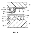
- Fig. 6 is an enlarged perspective view showing another modified example of the connection portion 23 of the male connector 10 according to the embodiment of the present invention.
- connection portion 23 extends long in the facing region of the connection portion 23 of the terminal 20 and the distal area 23C does not face the top face 34A of the sidewall 34 of the housing 31 of the female connector 30, the mating connector.
- the solder barrier layer 24 can be formed except the distal area 23C. Solder swelling occurs in the distal area 23C. Accordingly, the solder connection at the connection portion 23 becomes stranger. Further, the solder connection can be visually confirmed with ease due to the solder swelling. Accordingly, when the solder barrier layer 24 is formed except the distal area 23C, the revolving solder barrier layer 24A can be formed as in the case of Fig. 5 .
- Fig. 7 is an enlarged perspective view showing a further modified example of the connection portion 23 of the male connector 10 according to the embodiment of the present invention. It is preferred that the revolving solder barrier layer 24A be formed near a border position with the second contact portion 22B. Fig. 7 shows a case in which the solder barrier layer is not formed in the distal area 23C in the revolving solder barrier layer 24A.
- Figs. 8 (A) and 8 (B) are sectional views showing the male connector 10 and the female connector 30 according to another embodiment of the present invention. More specifically. Fig. 8 (A) is a sectional view showing the male connector 10 and the female connector 30 before the male connector 10 is fitted into the female connector 30, and Fig. 8 (B) is a sectional view showing the male connector 10 and the female connector 30 after the male connector 10 is fitted into the female connector 20.
- the top face 34A of the sidewall 34 of the housing 31 is formed to be in a step shape and a residual portion 34A-2 is recessed with respect to an adjacent portion 34A-1.
- a portion that corresponds to the solder barrier layer 24 is the adjacent portion 34A-1 with respect to the solder barrier layer 24.
- An area that corresponds to the adjacent portion 34A-1 with respect to the male connector 10 is the nearest facing region.
- connection portion 23 of the terminal 20 of the male connector 10 can broaden the distal area in which the solder barrier layer is not formed.
- the solder swelling improves the connection strength. Further, solder can be confirmed visually with ease.
- the residual portion 34A-2 that corresponds to the distal area is recessed from the adjacent portion 34A-1 in the sidewall 34 of the housing 31 of the female connector 30. Accordingly, even if there is solder swelling, as shown in Fig. 8(B) , the solder swelling is not adjacent to the top face 34A of the sidewall 34 upon fitting of the connectors. That is, the fitting of the connectors is not inhibited.
Abstract

Description
- The present invention relates to a male electrical connector to be attached to a circuit board (hereinafter called "male connector") and an electrical connector assembly for a circuit board (hereinafter called "connector assembly") having the male electrical connector and a female electrical connector (hereinafter called "female connector") to be attached to another circuit board.
- Publication Reference has disclosed a connector assembly for a circuit board. According to Publication Reference, each of a male connector and a female connector is attached to a circuit board. Further, the male connector and the female connector are fitted with each other to connect in a direction perpendicular to a surface of the circuit board. Accordingly, when the male connector and the female connector are fitted, the circuit boards become parallel to each other. A terminal of the male connector forms a connection portion in a portion that extends outside a housing thereof along a surface of the circuit board. Further, the connection portion is connected to a corresponding circuit portion of the circuit board with solder.
- Publication Reference : Japanese Utility Model Publication No.
3055703 - In the female connector, a peripheral wall of a housing is situated outside with respect to a fitting portion of the male connector. Further, a top face of the peripheral wall faces a connection portion of the male connector. The top face of the peripheral wall is adjacent to and faces the connection portion of a terminal of the male connector.
- The terminal of the male connector is connected with the circuit portion of the circuit board with solder in the connection portion. Molten solder rises from a solder connection surface of the connection portion due to surface tension. Further, the molten solder may reach a surface other than the solder connection surface that is tangent to the circuit portion. That is, a phenomenon called a "solder rising" occurs.
- The molten solder rises to a side edge surface of the connection portion due to the solder rising; thereby forming a fillet shape portion between a side edge surface and a surface of the circuit portion, thereby improving strength of the solder connection.
- The solder rising does not stop at the side edge surface of the connection portion. Instead, the solder rising proceeds further to reach a facing region in which the solder connection surface faces an opposite side surface of the solder connection surface, or a top face of a peripheral wall of the female connector (mating connector).
- Further, a swelling in the facing region of the connection portion may be formed there. The solder connection of the connection surface can be visually confirmed due to the solder rising. On the other hand, the connection portion may collide with the top face of the housing peripheral wall of the female connector due to the solder swelling in the facing region of the connection portion, thereby making it difficult to fit the male connector and the female connector.
- To this end, in Publication Reference, a space is formed as an escape portion, so that it is easy to fit the male connector and the female connector even when the male connector has the solder swelling in the connection portion. The escape portion is recessed from the top face of the housing peripheral wall of the female connector.
- According to Publication Reference, the escape portion of the female connector can prevent a trouble caused by the solder swelling in the connection portion of the terminal of the male connector. It should be noted, however, that it is necessary to provide the escape portion with a depth sufficiently larger than an expected amount of the solder swelling to certainly prevent the trouble. When a size of the escape portion increases, a size of the female connector increases as well in a fitting direction unless a special attention is paid to a size and an arrangement of the terminal.
- As described above, the solder swelling caused by the solder rising can inhibit a complete fitting of the male connector and the female connector. Further, when an automatic quantitative soldering is conducted, an amount of the solder may become insufficient in the solder connection portion by an amount corresponding to the solder rises, thereby decreasing the connection strength. Accordingly, the escape portion of the female connector may prevent the problem in the first case, but does not in the latter case.
- In view of the problems described above, an object of the present invention is to provide a male connector for a circuit board and a connector assembly comprising the male connector and a female connector for a circuit board. In the present invention, it is possible to prevent the male connector from insufficiently fitting to the female connector, and to provide solder with a sufficient amount in a solder connection portion. Further, it is possible to minimize a solder rising and maintain strength of a fillet shape portion.
- Further objects of the invention will be apparent from the following description of the invention.
- The above object is achieved by the invention recited in
claim 1. - In order to attain the objects described above, according to the present invention, a male connector is attached to a circuit board and fits with a female connector in a fitting direction perpendicular to a surface of the circuit board. A terminal of the male connector extends outside a housing thereof in parallel to the surface of the circuit board. The terminal has a connection portion that is connected with a circuit portion of the circuit board with solder. When the male connector and the female connector are fitted with each other, the connection portion has a facing region which faces a top face of a peripheral wall of a housing of the female connector in the fitting direction.
- According to the present invention, the terminal includes a solder barrier layer formed at least in a nearest facing region of the facing region of the connection portion of the terminal. The nearest facing region is situated to be closest to the top face of the peripheral wall in the fitting direction.
- In the present invention, the solder barrier layer is a surface layer of the terminal that is provided as a region in which molten solder has poor solderability property with respect to the terminal.
- In general, the terminal is plated with nickel as a base layer. The nickel plated layer has poor solderability property and is not suitable as the solder connection portion of the terminal. Accordingly, the terminal is often plated with copper or gold on a top of the nickel plate. The copper or gold plated surface has good solderabiliby property.
- In this case, for example, a partial region that is not plated with copper or gold may be provided. A surface layer of such a region becomes a layer plated with nickel, which can be a solder barrier layer.
- In the present invention, a material forming the solder barrier layer or a method of forming the solder barrier layer is not limited, and may be operable by any publicly known method. For example, a surface layer may be formed of an oxide layer, a resist ink, and the like as the solder barrier layer. It is sufficient that a material having poorer solderability than that of a portion to be connected to the terminal with solder is provided as the solder barrier layer in the nearest facing region.
- In the present invention, the solder barrier layer is formed at least in the nearest facing region of the facing region in which the connection portion of the terminal of the male connector faces the female connector. Accordingly, a solder swelling due to solder rising does not occur in the nearest facing region.
- Accordingly, it is easy to fit the male connector to the female connector to a specific depth. Further, an influence of a solder shortage in the solder connection surface is minimized. At the same time, the solder barrier layer is not provided on a side edge surface of the connection portion, thereby allowing the solder rising. Accordingly, the solder connection strength is sufficiently obtained in the fillet shape portion.
- According to the present invention, it is preferred that the solder barrier layer in the nearest facing region extends from a portion on a base portion side toward a peripheral surface of the terminal in a band shape in an extending direction of the connection portion. The solder barrier layer having a band shape revolves around the peripheral surface.
- Accordingly, the solder barrier layer prevents solder from traveling from the connection portion of the terminal to the base portion side at any position in a circular direction of the terminal. Further, the solder barrier layer having a band shape is situated on the base portion side in the extending direction. Accordingly, almost an entire range in the connection portion has good solderability, thereby ensuring solder strength.
- According to the present invention, it is preferred that the nearest facing region be formed on the base portion side in the extending direction of the connection portion. Accordingly, the solder swelling is prevented in an inner range in the connection portion extending direction more than in a portion in which the nearest facing region is provided, thereby ensuring a sufficient fitting depth of the male connector in the range.
- In this case, a facing direction distance with the female connector outside the range is longer than that of the range. Accordingly, the fitting of the male connector is not inhibited even when the solder swelling occurs outside the range. Further, the solder connection portion has a sufficient amount of solder and connection strength is improved due to the solder rising. Further, solder can be visually confirmed.
- According to the present invention, a connector assembly comprises the male connector and the female connector. The male connector and the female connector are attached to the respective circuit boards and fitted with each other in the fitting direction perpendicular to the surfaces of the circuit boards.
- Further, the connector assembly includes at least the connection portion and the facing region. In the connection portion, the terminal of the male connector extends outwardly from the housing thereof in parallel to the surface of the circuit board. Further, the connection portion is connected to the circuit portion of the circuit board with solder. In the facing region, the connection portion of the terminal of the male connector faces the top face of the peripheral wall of the housing of the female connector in the fitting direction when the male connector and the female connector are fitted with each other.
- According to the present invention, the connector assembly includes the solder barrier layer d at least in the nearest facing region in which the connection portion of the terminal of the male connector is situated nearest to the peripheral wall top face in the fitting direction of the facing region.
- As described above, the solder barrier layer is provided in the nearest facing region in the connection portion of the terminal of the male connector. Accordingly, there is no solder swelling in the region. Further, the fitting of the connector assembly is ensured up to a specific depth. Accordingly, the connectors are connected with each other securely. Further, a height of the connector assembly in the fitting direction does not have to be excessively large in consideration of the solder swelling, thereby reducing a size of the connector assembly in the direction.
- According to the present invention, the peripheral wall top face of the housing of the female connector may be formed so that a portion that corresponds to the facing region of the connection portion of the terminal of the male connector comprises an adjacent portion that corresponds to the nearest facing region and a residual portion. The residual portion is recessed from the adjacent portion in the fitting direction.
- In this case, the connection portion of the terminal of the male connector is provided with the solder barrier layer in the nearest facing region and there is no solder swelling there. Accordingly, the male connector and the female connector are fitted with each other up to a specific depth without any obstructions. The solder barrier layer is not necessarily provided in a region other than the nearest facing region. Accordingly, there can be the solder swelling. When the residual portion is recessed from the adjacent portion in the female connector, it is easy to deal with the solder swelling.
- According to the present invention, it is preferred that the terminal of the male connector be formed of a metal band body bending in a plate thickness direction thereof. Further, it is preferred that a terminal of the female connector be formed of a metal sheet maintaining a flat plate surface thereof.
- In the configuration described above, the plate thickness direction of the connection portion of the terminal of the male connector is aligned with the fitting direction of the male connector, and the plate surface becomes the solder connection surface. Accordingly, an area of the solder connection surface is enlarged, thereby increasing the solder connection strength and reducing a size of the connector assembly in the fitting direction due to the solder barrier layer.
- As described above, according to the present invention, the solder barrier layer is provided in the nearest facing region of the facing region that faces the female connector in the connection portion of the terminal of the male connector. The male connector is connected to the circuit board with solder. Further, the facing region that faces the female connector is situated on the opposite side of the solder connection surface.
- Accordingly, it is possible to prevent the solder rising to the nearest facing region, and no solder swelling occurs in the region. Accordingly, the male connector can be very close to or adjacent to the housing peripheral wall of the female connector in the region, thereby making it easy to fit the male connector to the female connector.
- Further, the connectors can be low-profiled. Further, there is no solder rising; thereby preventing the solder connection strength from being deteriorated without causing a shortage of solder in the solder connection portion. In addition, the solder rising occurs from the solder connection surface on the side edge surface of the connection portion in which the solder barrier layer is not provided. Accordingly, the fillet shape portion is provided there, thereby ensuring the solder connection strength.
- Embodiments of the invention will now be described by way of example with respect to the accompanying drawings, in which:
-
Fig. 1 is a perspective view showing a male connector according to an embodiment of the present invention; -
Fig. 2 is a perspective view showing a female connector according to the embodiment of the present invention; -
Figs. 3(A) and 3(B) are sectional views showing the male connector and the female connector taken along a line passing through terminals thereof, whereinFig. 3(A) is a sectional view showing the male connector and the female connector before the male connector is fitted into the female connector, andFig. 3(B) is a sectional view showing the male connector and the female connector after the male connector is fitted into the female connector; -
Fig. 4 is an enlarged perspective view showing a connection portion of the male connector according to the embodiment of the present invention; -
Fig. 5 is an enlarged perspective view showing a modified example of the connection portion of the male connector according to the embodiment of the present invention; -
Fig. 6 is an enlarged perspective view showing another modified example of the connection portion of the male connector according to the embodiment of the present invention; -
Fig. 7 is an enlarged perspective view showing a further modified example of the connection portion of the male connector according to the embodiment of the present invention; and -
Figs. 8(A) and 8(B) are sectional views showing a male connector and a female connector according to another embodiment of the present invention, whereinFig. 8(A) is a sectional view showing the male connector and the female connector before the male connector is fitted into the female connector, andFig. 8(B) is a sectional view showing the male connector and the female connector after the male connector is fitted into the female connector. - Hereunder, embodiments of the present invention will be explained with reference to the accompanying drawings.
- In the embodiment, a connector assembly comprises a male connector and a female connector. The male connector and the female connector are fitted with each other to be connected. Each of the male connector and the female connector is attached to a circuit board, so that surfaces of the circuit boards are parallel to each other. Further, the male connector and the female connector are fitted with each other in a direction perpendicular to the surfaces of the circuit boards.
- In the embodiment, the male connector has a housing portion having a protruding shape, while the female connector has a housing portion having a recess shape. A contact portion of a terminal that is attached to the housing is situated in the housing portion. The male connector and the female connector are fitted with each other at the protruding portion and the recess portion described above, so that the contact potions contact with each other. Accordingly, the male connector and the female connector are electrically connected.
-
Fig. 1 is a perspective view showing amale connector 10 according to an embodiment of the present invention. InFig. 1 , a circuit board to which themale connector 10 is attached is not shown. Arecess portion 12 is formed in a center portion of ahousing 11 of themale connector 10. Thehousing 11 is flat and has a planar shape of approximate rectangle. Further, aperipheral wall 13 that protrudes from thehousing 11 is provided in themale connector 10. Theperipheral wall 13 comprises twosidewalls 14 in a longitudinal direction of thehousing 11 andedge walls 15 that connect thesidewalls 14 on the both edges of the longitudinal direction. - A plurality of a terminal 20 is arranged and held at specific intervals in the longitudinal direction of the
sidewall 14. Ametal fixture 26 is attached to be adjacent to the terminal 20 that is arranged on each edge of the rows of the plurality of the terminal 20. The terminal 20 and themetal fixture 26 will be explained below. -
Dent portions 15A are formed in center positions of theedge walls 15 of thehousing 11. Thedent portion 15 pierces theedge wall 15 in the longitudinal direction in which thesidewalls 14 extend. Further, thedent portion 15 opens upward. - The
male connector 10 connects thedent portions 15A of theedge walls 15 that face each other. Further, themale connector 10 is symmetrical with respect to an axis line that extends in the longitudinal direction. Further, themale connector 10 is symmetrical with respect to a centerline that is perpendicular to the axis line in a center of the longitudinal direction thereof. - As shown in
Fig. 1 , themale connector 10 is attached to a circuit board P1. The terminal 20 of themale connector 10 is made through bending and forming a metal member having a band shape in a plate thickness direction thereof. Further, theterminals 20 are arranged and held at specific intervals in thesidewalls 14 of thehousing 11. -
Figs. 3(A) and 3(B) are sectional views showing themale connector 10 and thefemale connector 30 taken along a line that passes through the terminals. More specifically,Fig. 3 (A) is a sectional view showing themale connector 10 and thefemale connector 30 before themale connector 10 is fitted into thefemale connector 30.Fig. 3(B) is a sectional view showing themale connector 10 and thefemale connector 30 after themale connector 10 is fitted into thefemale connector 30. - The
male connector 10 shown inFigs. 3(A) and 3(B) faces with respect to thefemale connector 30, a mating connector in a fitting direction. That is, themale connector 10 is vertically flipped from that shown inFig. 1 . - The terminal 20 comprises an attached
portion 21, acontact portion 22, and aconnection portion 23. The attachedportion 21 is formed to fit into aterminal holding groove 16 from the top face of thesidewall 14 of the housing 11 (a top face inFig. 1 , a lower surface inFig. 3(A) ). - The
terminal holding groove 16 is formed to extend to the inner and outer wall surfaces of thesidewall 14. Thecontact portion 22 is formed in the inner and outer surfaces of the attachedportion 21. Theconnection portion 23 is bent in an L-character shape outside of thesidewall 14 and extends along a surface of the circuit board P1. Thecontact portion 22 comprises afirst contact portion 22A and asecond contact portion 22B. - In the embodiment, the
first contact portion 22A is formed inside of thesidewall 14, or the inner surface that faces therecess portion 12. Further, thesecond contact portion 22B is situated outside of thesidewall 14. Lockingportions 22A-1 and 22B-1 are provided in thefirst contact portion 22A and thesecond contact portion 22B, respectively, in order to maintain a stable contact position with a corresponding contact portion of the terminal of the female connector, or the mating connector. The lockingportions 22A-1 and 22B-1 are slightly recessed. - When the
male connector 10 is fitted into thefemale connector 30, theconnection portion 23 has a region that faces the housing of thefemale connector 30 on the opposite surface of the surface that is tangent to the circuit board P1. - The
female connector 30 will be explained below. In the embodiment, the region is called a "facing region". In the embodiment, a surface of the facing region is asurface layer 24, which has poorer solderability than that of surfaces of the other portions. The surface layer with poor solderability is called asolder barrier layer 24. - A corresponding portion of the housing of the female connector that the facing region faces in the embodiment can form a surface having a step shape. In the embodiment, a portion of the facing region that is nearest to the corresponding portion is called the nearest facing region. Similarly, when the connection portion forms a surface having a step shape, the region in which the facing surfaces are nearest to each other is called the nearest facing region.
- In the embodiment, the terminal 20 is nickel plated as an under layer. Further, the terminal 20 is copper plated or gold plated. The copper plate and the gold plate have good conduction and solderability, while the nickel plate has poor solderability.
- In the embodiment, the nickel plate as an under layer is exposed to form the
solder barrier layer 24 while preventing a necessary portion of the facing region from being copper plated or gold plated. -
Fig. 4 is an enlarged perspective view showing theconnection portion 23 of themale connector 10 according to the embodiment of the present invention. As shown inFig. 4 , a whole surface of amaterial 23A of theconnection portion 23 is plated with a nickel plate 23B as an under layer. Thematerial 23A has a flat band shape. Further, the whole surface of thematerial 23A of theconnection portion 23 except the facing region is further plated with agold plate 23C. - A required portion of the facing region is masked after plated with the nickel plate 23B as an under layer. Further, the terminal is gold plated. When the masking is removed, the nickel plate 23B forms the
solder barrier layer 24 in the required portion of the facing region. -
Fig. 5 is an enlarged perspective view showing a modified example of theconnection portion 23 of themale connector 10 according to the embodiment of the present invention. As shown inFig. 5 , thesolder barrier layer 24 ofFig. 4 further have a revolvingsolder barrier layer 24A. The revolvingsolder barrier layer 24A extends in a band shape on a surrounding surface of theconnection portion 23. - In the embodiment, each of the
metal fixtures 26 is attached to thesidewall 14, along with theterminals 20, on the outer positions with respect to an arrangement range of a set of theterminals 20 that is arranged and held on thesidewalls 14 of thehousing 11. Themetal fixture 26 is manufactured in a similar way with the terminal 20 except that themetal fixture 26 does not have a contact portion. - The
metal fixture 26 comprises an attached portion 26A and a fixed portion 26B. The attached portion 26A is bent in the plate thickness direction thereof to form an L-character shape. Further, the attached portion 26A is attached to and held by a holding groove that is formed on an outer surface of thesidewall 14 of thehousing 11. The fixed portion 26B extends in parallel and along with theconnection portion 23 of the terminal 20. - Similar to the
connection portion 23 of the terminal 20, the fixed portion 26B is connected to the circuit board P1 with solder on the surface that faces the circuit board P1. The surface of the opposite side is the facing region that faces the female connector. Accordingly, similar to the case of the terminal 20, the facing region is provided with a solder barrier layer. - In the embodiment, the
female connector 30 that receives themale connector 10 has an appearance as shown inFig. 2 and a section as shown inFig. 3(A) . - As shown in
Fig. 2 , thefemale connector 30 is attached to a circuit board P2 (not shown inFig. 2 ) when used. Further,terminals 50 and ametal fixture 58 are attached to ahousing 31. - The
housing 31 is provided with a receivingrecess portion 32 inside of aperipheral wall 33. Theperipheral wall 33 comprises twosidewalls 34 andedge walls 35. Thesidewall 34 extends in a longitudinal direction. The longitudinal direction is a terminal arrangement direction. Theedge wall 35 is provided on each end of the longitudinal direction. Further, thehousing 31 has a protrudingportion 36 having an island shape. - The protruding
portion 36 is surrounded by the receivingrecess portion 32. The connectingportions 37 connect the protrudingportion 36 to theedge walls 35 to reinforce on both ends of the longitudinal direction. The receivingrecess portion 32 receives theperipheral wall 13 of themale connector 10. Further, the protrudingportion 36 fits into therecess portion 12 of themale connector 10. - At that time, the connecting
portion 37 enters into thedent portion 15A of themale connector 10. Further, atop face 34A of thesidewall 34 is recessed in a step shape with respect to atop face 35A of theedge wall 35. When themale connector 10 and thefemale connector 30 are fitted with each other, the facing region of theconnection portion 23 of the terminal 20 of themale connector 10 is substantially tangent to thetop face 34A of thesidewall 34 of thefemale connector 30. - The terminal 50 of the
female connector 30 has an outer shape in which a metal sheet is processed while maintaining the planarity of the metal sheet. As shown inFig. 3(A) , theterminal 50 of thefemale connector 30 is held by thehousing 31 at a position that corresponds to theterminal 20 of themale connector 10 in the longitudinal direction. - As shown in
Fig. 3(A) , the terminal 50 comprises abase portion 51, afirst contact arm 52, asecond contact arm 53, a first attachedarm 54, a second attachedarm 55, a third attachedarm 56, and aconnection portion 57. - The
base portion 51 is positioned in a lower surface of thehousing 31 and extends to be parallel to the lower surface. Thefirst contact arm 52 and thesecond contact arm 53 extend upward from thebase portion 51 in a middle portion of a direction in which thebase portion 51 extends. The first attachedarm 54, the second attachedarm 55, and the third attachedarm 56 extend upward from thebase portion 51 on both sides with respect to thefirst contact arm 52 and thesecond contact arm 53, respectively. Further, thebase portion 51 extends outside of the housing to form theconnection portion 57. Further, afirst contact portion 52A and asecond contact portion 53A are formed in thefirst contact arm 52 and thesecond contact arm 53, respectively. - The
first contact portion 52A and thesecond contact portion 53A face each other and protrude on the top edges thereof. The first attachedarm 54 is situated on a backside of thefirst contact arm 52. Further, the first attachedarm 54 is positioned in a center side of the connector. - The second attached
arm 55 and the third attachedarm 56 are situated on a back of thesecond contact arm 53. Further, the second attachedarm 55 and the third attachedarm 56 are positioned near an outer side of the connector. Thefirst contact arm 52 and thesecond contact arm 53 have an elasticity to bend in a direction in which thefirst contact portion 52A and thesecond contact portion 53A are away from each other, respectively. Thefirst contact arm 52 and thesecond contact arm 53 are bent when a contact pressure is received from theterminal 20 of themale connector 10, the mating connector, in thefirst contact portion 52A and thesecond contact portion 53A, respectively. - In the embodiment,
metal fixtures 58 are attached to corresponding grooves of thehousing 31 outside of arrangement ranges of theterminals 50. Themetal fixture 58 has a plate shape. Further, a lower edge of the metal fixture is exposed from a bottom surface of the connector to be fixed to the circuit board with solder. -
Terminal holding grooves 38 are formed in thehousing 31 to correspond to a shape of theterminals 50. Theterminal holding groove 38 is situated in a position that corresponds to each terminal 20 of themale connector 10 in a longitudinal direction of thehousing 31 and holds the terminal 50 there. As shown inFig. 3(A) , abottom groove 39 covers a range from the protrudingportion 36 to thesidewall 34 in theterminal holding groove 38 in the lower surface of thehousing 31. Further, branched grooves of a variety extend upward. - As shown in
Fig. 3(A) , aninner holding groove 40 and anouter holding groove 41 are formed to open toward the receivingrecess portion 32 on an inner surface of the wall portion of the receivingrecess portion 32. Theinner holding groove 40 and the outer holdinggroove 41 face each other and extend upward from thebottom groove 39 ofterminal holding groove 38. - A first holding
groove 42, asecond holding groove 43, and athird holding groove 44 are provided on the opposite side of the receivingrecess portion 32 with respect to theinner holding groove 40. Thefirst holding groove 42 extends inside of the protrudingportion 36 having an island shape and passes through upward. Thesecond holding groove 43 extends inside of thesidewall 34. Thethird holding groove 44 is provided on an outer surface of thesidewall 34. - The
first contact arm 52 and thesecond contact arm 53 of the terminal 50 are stored in theinner holding groove 40 and the outer holdinggroove 41 of theterminal holding groove 38, respectively. The first attachedarm 54 is stored in the first holdinggroove 42. Further, the second attachedarm 55 and the third attachedarm 56 are stored in thesecond holding groove 43 and thethird holding groove 44, respectively. - The first attached
arm 54 is loosely fitted into the first holdinggroove 42. The second attachedarm 55 is pressed to fit into thesecond holding groove 43. The third attachedarm 56 is pressed by a bottom surface of thethird holding groove 44. AccordingJ.y, the terminal 50 is held. - The
male connector 10 and thefemale connector 30 of the embodiment are constituted as described. Themale connector 10 and thefemale connector 30 are used as described below. - First, the
male connector 10 and thefemale connector 30 are attached to the circuit boards P1 and P2, respectively. That is, themale connector 10 and thefemale connector 30 are connected to the respective corresponding circuit portion in theconnection portion 23 of the terminal 20 and theconnection portion 57 of the terminal 50, respectively, with solder. Further, themetal fixture 26 of themale connector 10 and themetal fixture 58 of thefemale connector 30 are fixed to the respective corresponding portion of the circuit board with solder. - When the terminal 20 of the
male connector 10 is connected with the corresponding circuit portion of the circuit board P1 in theconnection portion 23 with solder, molten solder connects themale connector 10 and the circuit board P1 in the tangent area of theconnection portion 23 and the corresponding circuit portion with solder. Further, the molten solder reaches the side faces of theconnection portion 23 in which a fillet portion is formed. Accordingly, a contact area between theconnection portion 23 and the corresponding circuit portion is increased; and thereby improving the electrical property and strengthening a retention force in the circuit board of the connector. - The molten solder can further rise from the side faces of the
connection portion 23 to a free surface on the opposite side of the tangent area; that is, the facing region. Further, the molten solder can rise from the free surface to the base portion of theconnection portion 23. In the embodiment, however, as shown inFigs. 1 ,3(A) , and4 , thesolder barrier layer 24 is provided in the facing region that is the free surface of theconnection portion 23. Accordingly, even if the molten solder rises from the side faces of theconnection portion 23, the molten solder does not reach the facing region. Accordingly, the solder does not adhere to the facing region or is not swollen due to an adhesion. Similarly, the solder is not swollen in the fixed portion 26B of themetal fixture 26 of the male connector. - As shown in
Fig. 5 , when the revolvingsolder barrier layer 24A is provided, the molten solder does not proceed toward the housing side of the revolvingsolder barrier layer 24A. - Accordingly, as shown in
Fig. 3(B) , themale connector 10 that is attached to the circuit board P1 and thefemale connector 30 that is attached to the circuit board P2 are fitted with each other in a direction perpendicular to the surfaces of the circuit boards P1 and P2 so that the circuit boards P1 and P2 are parallel to each other. - In the
male connector 10, the twocontact portions 22, or thefirst contact portion 22A and thesecond contact portion 22B, of the terminal 20 that are supported on thesidewalls 14 enter inside of the receivingrecess portion 32 of thefemale connector 30. Further, the protrudingportion 36 of thefemale connector 30 enters into therecess portion 12 of themale connector 10. The protrudingportion 36 has an island shape. - Accordingly, the
first contact portion 22A and thesecond contact portion 22B elastically contact with thefirst contact portion 52A and thesecond contact portion 53A of the two contact arms of the terminal 50, or thefirst contact arm 52 and thesecond contact arm 53, respectively. The facing region in which theconnection portion 23 of the terminal 20 of themale connector 10 faces the top face of thesidewall 34 of thefemale connector 30 contacts or becomes near the top face. Accordingly, the connectors are completely fitted with each other to a specific depth. - The present invention is not limited to the embodiments shown in
Figs. 1 to 5 , and various changes can be made.Fig. 6 is an enlarged perspective view showing another modified example of theconnection portion 23 of themale connector 10 according to the embodiment of the present invention. - First, in the
male connector 10, as shown inFig. 6 , it is not necessary to form a solder barrier layer in thedistal area 23C when theconnection portion 23 extends long in the facing region of theconnection portion 23 of the terminal 20 and thedistal area 23C does not face thetop face 34A of thesidewall 34 of thehousing 31 of thefemale connector 30, the mating connector. - The
solder barrier layer 24 can be formed except thedistal area 23C. Solder swelling occurs in thedistal area 23C. Accordingly, the solder connection at theconnection portion 23 becomes stranger. Further, the solder connection can be visually confirmed with ease due to the solder swelling. Accordingly, when thesolder barrier layer 24 is formed except thedistal area 23C, the revolvingsolder barrier layer 24A can be formed as in the case ofFig. 5 . -
Fig. 7 is an enlarged perspective view showing a further modified example of theconnection portion 23 of themale connector 10 according to the embodiment of the present invention. It is preferred that the revolvingsolder barrier layer 24A be formed near a border position with thesecond contact portion 22B.Fig. 7 shows a case in which the solder barrier layer is not formed in thedistal area 23C in the revolvingsolder barrier layer 24A. -
Figs. 8 (A) and 8 (B) are sectional views showing themale connector 10 and thefemale connector 30 according to another embodiment of the present invention. More specifically.Fig. 8 (A) is a sectional view showing themale connector 10 and thefemale connector 30 before themale connector 10 is fitted into thefemale connector 30, andFig. 8 (B) is a sectional view showing themale connector 10 and thefemale connector 30 after themale connector 10 is fitted into thefemale connector 20. - In the
female connector 30, when thesolder barrier layer 24 is formed only in a portion of the base portion side of theconnection portion 23 of the terminal 20 of themale connector 10 in the extending direction of theconnection portion 23, as shown inFig. 8 (A) , thetop face 34A of thesidewall 34 of thehousing 31 is formed to be in a step shape and aresidual portion 34A-2 is recessed with respect to anadjacent portion 34A-1. A portion that corresponds to thesolder barrier layer 24 is theadjacent portion 34A-1 with respect to thesolder barrier layer 24. An area that corresponds to theadjacent portion 34A-1 with respect to themale connector 10 is the nearest facing region. - Accordingly, the
connection portion 23 of the terminal 20 of themale connector 10 can broaden the distal area in which the solder barrier layer is not formed. As a result, the solder swelling improves the connection strength. Further, solder can be confirmed visually with ease. Further, theresidual portion 34A-2 that corresponds to the distal area is recessed from theadjacent portion 34A-1 in thesidewall 34 of thehousing 31 of thefemale connector 30. Accordingly, even if there is solder swelling, as shown inFig. 8(B) , the solder swelling is not adjacent to thetop face 34A of thesidewall 34 upon fitting of the connectors. That is, the fitting of the connectors is not inhibited. - The disclosure of Japanese Patent Application No.
2007-150054, filed on June 6, 2007 - While the invention has been explained with reference to the specific embodiments of the invention, the explanation is illustrative and the invention is limited
Claims (6)
- A male connector to be attached to a circuit board for fitting into a female connector in a fitting direction perpendicular to the circuit board, comprising:a first housing; anda terminal extending outside the housing in parallel to the circuit board, said terminal including a connection portion to be connected with a circuit portion of the circuit board with solder, said connection portion including a facing region facing a top face of a peripheral wall of a second housing of the female connector in the fitting direction when the male connector is fitted into the female connector, said facing region including a solder barrier layer at least in a nearest facing region thereof situated to be closest to the top face in the fitting direction.
- The male connector according to claim 1, wherein said solder barrier layer is formed in a band shape extending from a portion of the terminal on a base portion side thereof toward a peripheral surface thereof in an extending direction of the connection portion.
- The male connector according to claim 2, wherein said nearest facing region is formed on the base portion side in the extending direction of the connection portion.
- A connector assembly, comprising:a female connector to be attached to a first circuit board, said female connector including a first terminal and a first housing having a peripheral wall; anda male connector to be attached to a second circuit board and fitted into the female connector in a fitting direction,wherein said male connector includes a second, housing and a second terminal extending outside the second housing in parallel to the second circuit board, said second terminal including a connection portion to be connected with a circuit portion of the second circuit board with solder, said connection portion including a facing region facing a top face of the peripheral wall in the fitting direction when the male connector is fitted into the female connector, said facing region including a solder barrier layer at least in a nearest facing region thereof situated to be closest to the top face in the fitting direction.
- The connector assembly according to claim 4, wherein said top face includes a portion corresponding to the facing region, said portion including an adjacent portion corresponding to the nearest facing region and a residual portion, said residual portion being recessed from the adjacent portion in the fitting direction.
- The connector assembly according to claim 4, wherein said first terminal is formed of a metal sheet maintaining a flat plate surface thereof, said second terminal being formed of a metal band body bending in a plate thickness direction thereof.
Applications Claiming Priority (1)
| Application Number | Priority Date | Filing Date | Title |
|---|---|---|---|
| JP2007150054A JP4454036B2 (en) | 2007-06-06 | 2007-06-06 | Male electrical connector for circuit board and electrical connector assembly |
Publications (2)
| Publication Number | Publication Date |
|---|---|
| EP2001084A1 true EP2001084A1 (en) | 2008-12-10 |
| EP2001084B1 EP2001084B1 (en) | 2013-08-14 |
Family
ID=39651054
Family Applications (1)
| Application Number | Title | Priority Date | Filing Date |
|---|---|---|---|
| EP08104238.4A Expired - Fee Related EP2001084B1 (en) | 2007-06-06 | 2008-06-03 | Male connector and connector assembly |
Country Status (6)
| Country | Link |
|---|---|
| US (1) | US7625244B2 (en) |
| EP (1) | EP2001084B1 (en) |
| JP (1) | JP4454036B2 (en) |
| KR (1) | KR101032584B1 (en) |
| CN (1) | CN101320859B (en) |
| TW (1) | TW200849741A (en) |
Families Citing this family (26)
| Publication number | Priority date | Publication date | Assignee | Title |
|---|---|---|---|---|
| JP4954050B2 (en) * | 2007-12-20 | 2012-06-13 | モレックス インコーポレイテド | Terminals and connectors |
| US20100130068A1 (en) * | 2008-11-25 | 2010-05-27 | Yung-Chi Peng | Board-to-board connector assembly |
| JP2011029111A (en) * | 2009-07-29 | 2011-02-10 | Molex Inc | Connector |
| JP4887412B2 (en) * | 2009-09-18 | 2012-02-29 | ヒロセ電機株式会社 | Circuit board electrical connector |
| JP4901944B2 (en) * | 2009-12-03 | 2012-03-21 | ヒロセ電機株式会社 | Electrical connector |
| JP5479406B2 (en) * | 2011-06-30 | 2014-04-23 | 日本航空電子工業株式会社 | connector |
| US8888506B2 (en) * | 2013-01-29 | 2014-11-18 | Japan Aviation Electronics Industry, Limited | Connector |
| CN203180152U (en) * | 2013-02-07 | 2013-09-04 | 番禺得意精密电子工业有限公司 | Electric connector |
| CN106848654B (en) * | 2013-02-27 | 2019-06-04 | 松下知识产权经营株式会社 | Connector and the plug piece and socket piece used in the connector |
| JP6537890B2 (en) * | 2014-09-26 | 2019-07-03 | 日本航空電子工業株式会社 | connector |
| TWM520732U (en) * | 2015-09-25 | 2016-04-21 | Advanced Connectek Inc | Electric connector of plug and electric connector of socket |
| JP6807218B2 (en) | 2016-11-18 | 2021-01-06 | モレックス エルエルシー | connector |
| CN108232526B (en) * | 2016-12-21 | 2020-04-24 | 富士康(昆山)电脑接插件有限公司 | Electric connector and combination thereof |
| CN108258484B (en) * | 2016-12-28 | 2020-02-21 | 富士康(昆山)电脑接插件有限公司 | Electric connector and combination thereof |
| CN108933365B (en) * | 2017-05-26 | 2021-06-18 | 富士康(昆山)电脑接插件有限公司 | Electrical connector |
| JP6582083B2 (en) * | 2018-03-09 | 2019-09-25 | 京セラ株式会社 | Connectors and electronic devices |
| CN112335137B (en) * | 2018-06-22 | 2022-04-05 | 株式会社藤仓 | Electrical connector |
| TWI823997B (en) * | 2018-08-28 | 2023-12-01 | 英屬開曼群島商鴻騰精密科技股份有限公司 | Card edge connector |
| JP2020077490A (en) * | 2018-11-06 | 2020-05-21 | Smk株式会社 | Electric connector, and electric connector set |
| JP7202866B2 (en) * | 2018-12-03 | 2023-01-12 | ヒロセ電機株式会社 | TERMINAL FOR BOARD CONNECTOR, CONNECTOR AND CONNECTOR MANUFACTURING METHOD |
| JP6986039B2 (en) * | 2019-03-15 | 2021-12-22 | ヒロセ電機株式会社 | Electrical connector and electrical connector assembly |
| CN209571614U (en) * | 2019-04-18 | 2019-11-01 | 富士康(昆山)电脑接插件有限公司 | Electric connector and its docking connector |
| US11095059B2 (en) * | 2019-04-25 | 2021-08-17 | Molex, Llc | Connector |
| WO2021000152A1 (en) * | 2019-06-30 | 2021-01-07 | 瑞声声学科技(深圳)有限公司 | Multi-pole connector |
| JP7196028B2 (en) * | 2019-07-04 | 2022-12-26 | 日本航空電子工業株式会社 | connector assembly |
| JP1663235S (en) | 2020-02-13 | 2020-07-06 |
Citations (6)
| Publication number | Priority date | Publication date | Assignee | Title |
|---|---|---|---|---|
| JPH0355703A (en) | 1989-07-25 | 1991-03-11 | Toshiba Lighting & Technol Corp | Fluorescent lamp device |
| WO2006130252A1 (en) * | 2005-04-18 | 2006-12-07 | Molex Incorporated | Board-to-board connector pair |
| JP2006351223A (en) * | 2005-06-13 | 2006-12-28 | Molex Inc | Narrow pitch connector for board to board |
| JP2007042410A (en) * | 2005-08-03 | 2007-02-15 | Molex Inc | Board-to-board connector |
| WO2007061233A1 (en) * | 2005-11-24 | 2007-05-31 | Yoon-Sik Choi | Connector |
| JP2007150054A (en) | 2005-11-29 | 2007-06-14 | Towa Corp | Sealing mechanism in resin sealing mold apparatus |
Family Cites Families (6)
| Publication number | Priority date | Publication date | Assignee | Title |
|---|---|---|---|---|
| JPH0255703U (en) | 1988-10-18 | 1990-04-23 | ||
| JP3617220B2 (en) * | 1996-11-26 | 2005-02-02 | 松下電工株式会社 | connector |
| JP2002008753A (en) * | 2000-06-16 | 2002-01-11 | Matsushita Electric Works Ltd | Connector |
| JP2004185866A (en) * | 2002-11-29 | 2004-07-02 | Toshiba Corp | Connector device, and manufacturing method of lead terminal for connector |
| US6881075B2 (en) * | 2003-07-08 | 2005-04-19 | Cheng Uei Precision Industry Co., Ltd. | Board-to-board connector |
| JP3860823B2 (en) * | 2004-08-19 | 2006-12-20 | 京セラエルコ株式会社 | Connector and portable terminal equipped with this connector |
-
2007
- 2007-06-06 JP JP2007150054A patent/JP4454036B2/en active Active
-
2008
- 2008-05-12 TW TW097117408A patent/TW200849741A/en not_active IP Right Cessation
- 2008-05-26 KR KR1020080048517A patent/KR101032584B1/en active IP Right Grant
- 2008-06-03 EP EP08104238.4A patent/EP2001084B1/en not_active Expired - Fee Related
- 2008-06-04 CN CN2008101259056A patent/CN101320859B/en active Active
- 2008-06-05 US US12/155,520 patent/US7625244B2/en active Active
Patent Citations (6)
| Publication number | Priority date | Publication date | Assignee | Title |
|---|---|---|---|---|
| JPH0355703A (en) | 1989-07-25 | 1991-03-11 | Toshiba Lighting & Technol Corp | Fluorescent lamp device |
| WO2006130252A1 (en) * | 2005-04-18 | 2006-12-07 | Molex Incorporated | Board-to-board connector pair |
| JP2006351223A (en) * | 2005-06-13 | 2006-12-28 | Molex Inc | Narrow pitch connector for board to board |
| JP2007042410A (en) * | 2005-08-03 | 2007-02-15 | Molex Inc | Board-to-board connector |
| WO2007061233A1 (en) * | 2005-11-24 | 2007-05-31 | Yoon-Sik Choi | Connector |
| JP2007150054A (en) | 2005-11-29 | 2007-06-14 | Towa Corp | Sealing mechanism in resin sealing mold apparatus |
Also Published As
| Publication number | Publication date |
|---|---|
| JP4454036B2 (en) | 2010-04-21 |
| KR101032584B1 (en) | 2011-05-06 |
| TWI371893B (en) | 2012-09-01 |
| CN101320859A (en) | 2008-12-10 |
| EP2001084B1 (en) | 2013-08-14 |
| CN101320859B (en) | 2010-11-10 |
| US7625244B2 (en) | 2009-12-01 |
| TW200849741A (en) | 2008-12-16 |
| JP2008305603A (en) | 2008-12-18 |
| US20080305657A1 (en) | 2008-12-11 |
| KR20080107259A (en) | 2008-12-10 |
Similar Documents
| Publication | Publication Date | Title |
|---|---|---|
| EP2001084B1 (en) | Male connector and connector assembly | |
| EP1986279B1 (en) | Connector and connector connecting body | |
| EP2019455B1 (en) | Electrical connector | |
| US8961215B2 (en) | Electrical connector assembled component, plug connector, and receptacle connector | |
| JP3703665B2 (en) | Electrical connector connection structure | |
| US7588443B2 (en) | Board-to-board electrical connector assembly | |
| US20100210124A1 (en) | Electrical connector having grounding terminal having tail portion interconnected to metallic shell surrounding the connector | |
| EP1881563A1 (en) | Electrical connector | |
| US20140315419A1 (en) | Substrate connection structure using substrate connector | |
| CN109586063B (en) | Connector for substrate and combination thereof | |
| JP2007193949A (en) | Connector | |
| JPWO2020059210A1 (en) | Receptacle connector | |
| CN1681167B (en) | Shielded connector | |
| US7758366B2 (en) | Connector for electrical connection | |
| TWI437769B (en) | Electrical connectors for circuit boards | |
| JPH11339906A (en) | Substrate mount connector | |
| US7413475B2 (en) | Electrical connector having ground planes | |
| JP7283971B2 (en) | BOARD CONNECTOR AND BOARD CONNECTOR STRUCTURE | |
| JP7082500B2 (en) | Terminals, connectors, and connector devices | |
| JP2007115579A (en) | Electric connector for circuit board | |
| JP2020194637A (en) | Connector and board-equipped connector | |
| TWI837329B (en) | Electrical connector assembly | |
| CN2351867Y (en) | Electric connector | |
| JP2007250282A (en) | Surface mounted receptacle | |
| JP4766714B2 (en) | Electrical connector with ground plate |
Legal Events
| Date | Code | Title | Description |
|---|---|---|---|
| PUAI | Public reference made under article 153(3) epc to a published international application that has entered the european phase |
Free format text: ORIGINAL CODE: 0009012 |
|
| AK | Designated contracting states |
Kind code of ref document: A1 Designated state(s): AT BE BG CH CY CZ DE DK EE ES FI FR GB GR HR HU IE IS IT LI LT LU LV MC MT NL NO PL PT RO SE SI SK TR |
|
| AX | Request for extension of the european patent |
Extension state: AL BA MK RS |
|
| 17P | Request for examination filed |
Effective date: 20090604 |
|
| 17Q | First examination report despatched |
Effective date: 20090720 |
|
| AKX | Designation fees paid |
Designated state(s): DE FI GB |
|
| REG | Reference to a national code |
Ref country code: DE Ref legal event code: R079 Ref document number: 602008026707 Country of ref document: DE Free format text: PREVIOUS MAIN CLASS: H01R0004020000 Ipc: H01R0012710000 |
|
| GRAP | Despatch of communication of intention to grant a patent |
Free format text: ORIGINAL CODE: EPIDOSNIGR1 |
|
| RIC1 | Information provided on ipc code assigned before grant |
Ipc: H01R 43/02 20060101ALI20130206BHEP Ipc: H01R 12/57 20110101ALI20130206BHEP Ipc: H01R 12/71 20110101AFI20130206BHEP Ipc: H01R 4/02 20060101ALI20130206BHEP |
|
| GRAS | Grant fee paid |
Free format text: ORIGINAL CODE: EPIDOSNIGR3 |
|
| GRAA | (expected) grant |
Free format text: ORIGINAL CODE: 0009210 |
|
| AK | Designated contracting states |
Kind code of ref document: B1 Designated state(s): DE FI GB |
|
| REG | Reference to a national code |
Ref country code: GB Ref legal event code: FG4D |
|
| REG | Reference to a national code |
Ref country code: DE Ref legal event code: R096 Ref document number: 602008026707 Country of ref document: DE Effective date: 20131010 |
|
| PG25 | Lapsed in a contracting state [announced via postgrant information from national office to epo] |
Ref country code: FI Free format text: LAPSE BECAUSE OF FAILURE TO SUBMIT A TRANSLATION OF THE DESCRIPTION OR TO PAY THE FEE WITHIN THE PRESCRIBED TIME-LIMIT Effective date: 20130814 |
|
| PLBE | No opposition filed within time limit |
Free format text: ORIGINAL CODE: 0009261 |
|
| STAA | Information on the status of an ep patent application or granted ep patent |
Free format text: STATUS: NO OPPOSITION FILED WITHIN TIME LIMIT |
|
| 26N | No opposition filed |
Effective date: 20140515 |
|
| REG | Reference to a national code |
Ref country code: DE Ref legal event code: R097 Ref document number: 602008026707 Country of ref document: DE Effective date: 20140515 |
|
| REG | Reference to a national code |
Ref country code: DE Ref legal event code: R119 Ref document number: 602008026707 Country of ref document: DE |
|
| GBPC | Gb: european patent ceased through non-payment of renewal fee |
Effective date: 20140603 |
|
| REG | Reference to a national code |
Ref country code: DE Ref legal event code: R119 Ref document number: 602008026707 Country of ref document: DE Effective date: 20150101 |
|
| PG25 | Lapsed in a contracting state [announced via postgrant information from national office to epo] |
Ref country code: DE Free format text: LAPSE BECAUSE OF NON-PAYMENT OF DUE FEES Effective date: 20150101 |
|
| PG25 | Lapsed in a contracting state [announced via postgrant information from national office to epo] |
Ref country code: GB Free format text: LAPSE BECAUSE OF NON-PAYMENT OF DUE FEES Effective date: 20140603 |