EP2000887A1 - Inputting apparatus and inputting method - Google Patents
Inputting apparatus and inputting method Download PDFInfo
- Publication number
- EP2000887A1 EP2000887A1 EP07739615A EP07739615A EP2000887A1 EP 2000887 A1 EP2000887 A1 EP 2000887A1 EP 07739615 A EP07739615 A EP 07739615A EP 07739615 A EP07739615 A EP 07739615A EP 2000887 A1 EP2000887 A1 EP 2000887A1
- Authority
- EP
- European Patent Office
- Prior art keywords
- signal
- substrate
- signal line
- input apparatus
- reflected
- Prior art date
- Legal status (The legal status is an assumption and is not a legal conclusion. Google has not performed a legal analysis and makes no representation as to the accuracy of the status listed.)
- Granted
Links
Images


Classifications
-
- G—PHYSICS
- G06—COMPUTING; CALCULATING OR COUNTING
- G06F—ELECTRIC DIGITAL DATA PROCESSING
- G06F3/00—Input arrangements for transferring data to be processed into a form capable of being handled by the computer; Output arrangements for transferring data from processing unit to output unit, e.g. interface arrangements
- G06F3/01—Input arrangements or combined input and output arrangements for interaction between user and computer
- G06F3/02—Input arrangements using manually operated switches, e.g. using keyboards or dials
- G06F3/0202—Constructional details or processes of manufacture of the input device
-
- H—ELECTRICITY
- H01—ELECTRIC ELEMENTS
- H01P—WAVEGUIDES; RESONATORS, LINES, OR OTHER DEVICES OF THE WAVEGUIDE TYPE
- H01P5/00—Coupling devices of the waveguide type
- H01P5/04—Coupling devices of the waveguide type with variable factor of coupling
-
- H—ELECTRICITY
- H03—ELECTRONIC CIRCUITRY
- H03K—PULSE TECHNIQUE
- H03K17/00—Electronic switching or gating, i.e. not by contact-making and –breaking
- H03K17/94—Electronic switching or gating, i.e. not by contact-making and –breaking characterised by the way in which the control signals are generated
- H03K17/96—Touch switches
Definitions
- This invention relates to a thin-type input apparatus and to an input method.
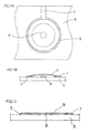
- Fig. 11 is an explanatory view illustrating the configuration of a key portion at a conventional operating portion used in a portable terminal.
- a top view of the conventional key portion is illustrated in Fig. 11A
- a sectional view of the conventional key portion is illustrated in Fig. 11B .
- the key portion illustrated in Fig. 11 includes a flexible key sheet placed in electrical insulation relative to a substrate 6 and having a recess with respect to the substrate 6, and a metal plate 9 secured in the recess as by an adhesive sheet or the like.
- FIG. 11B is an explanatory view illustrating the central portion of the metal plate 9 in the pressed state.
- a controller of the portable terminal detects the fact that the key portion has been pressed.
- Patent Document 1 describes a switch in which a piezoelectric element is provided on one surface of a substrate. Ultrasonic waves within the substrate that change if a finger touches the other surface of the substrate are detected, whereby contact with the finger is detected.
- Patent Document 1 Japanese Patent Application Laid-Open No. 7-282699 (paragraphs 0018 to 0043; Fig. 1 ).
- the key assembly process is performed in a clean room or the key portion must be constructed in such a manner that foreign matter will not penetrate into the gap after shipping.
- the piezoelectric element is provided on one surface of the substrate in the switch described in Patent Document 1, it is difficult to achieve a reduction in thickness.
- a main object of the present invention is to provide an input apparatus and method that enable a reduction in thickness and prevention of the occurrence of contact failure.
- an input apparatus including a substrate on a surface of which a signal line has been formed, and an insulating sheet disposed facing the surface of the substrate and having information, which represents a plurality of operating positions, indicated on a surface thereof that is opposite surface facing the substrate, characterized in that the apparatus comprises: signal transmitting means for outputting a signal to the signal line; reflected-wave detecting means for detecting a reflected wave of the signal that has been output by the signal transmitting means; and computing means for discriminating an operating position at which an operation has been performed, based upon the reflected wave detected by the reflected-wave detecting means.
- the signal line may be formed so as to pass through the vicinity of the operating positions in the insulating sheet, and a ground line at ground potential may be formed on the substrate in parallel with the signal line.
- the signal line may be formed so as to lengthen distance between a portion that passes through the vicinity of an operating position in the insulating sheet and a portion that passes through the vicinity of another operating position.
- the computing means may discriminate an operating position at which an operation has been performed, based upon signal strength of the signal that has been output by the signal transmitting means and signal strength of the reflected wave detected by the reflected-wave detecting means.
- the computing means may perform time domain reflectometry based upon signal strength of the signal that has been output by the signal transmitting means and signal strength of the reflected wave detected by the reflected-wave detecting means, and may discriminate an operating position at which an operation has been performed, based upon result of time domain reflectometry.
- the input apparatus may further comprise storage means in which a table correlating the result of time domain reflectometry (TDR) and entered instructions has been stored in advance, wherein the computing means specifies an entered instruction based upon the table stored by the storage means and the result of TDR.
- TDR time domain reflectometry
- the signal line may be formed on the substrate so as to have a circular portion
- the computing means may discriminate an operation that has been performed on the insulating sheet, based upon a change in the result of TDR.
- an input method which uses an input apparatus having a substrate on a surface of which a signal line has been formed, and an insulating sheet disposed facing the surface of the substrate and having information, which represents a plurality of operating positions, indicated on a surface thereof that is on a side opposite a surface facing the substrate, characterized in that the method comprises: a signal output step of signal transmitting means outputting a signal to the signal line; a reflected-wave detecting step of reflected-wave detecting means detecting a reflected wave of the signal that has been output by the signal transmitting means at the signal outputs step; and a computing step of computing means discriminating an operating position at which an operation has been performed, based upon the reflected wave detected by the reflected-wave detecting means at the reflected-wave detecting step.
- the input apparatus does not have a mechanical switch structure and, as a result, the input apparatus can be reduced in thickness and it is possible to prevent the occurrence of contact failure due to entry of foreign matter, etc.
- a coplanar line is constructed. If the finger of a user touches the operating position, therefore, a reflected wave of the signal that has been output by the signal transmitting means is produced and the reflected-wave detecting means can detect this reflected wave.
- the distance between the operating positions can be lengthened artificially to thereby enable lowering of the frequency of the signal that is output by the signal transmitting means.
- the input apparatus is capable of accommodating input of an instruction that conforms to movement of the finger of a user.
- FIG. 1 is a perspective view illustrating an example of the configuration of a key input apparatus (input apparatus) according to an exemplary embodiment of the present invention.
- the key input apparatus shown in Fig. 1 includes an elastic key sheet (insulating sheet) 1, the main ingredient of which is silicone rubber or the like, and a substrate 6 on which a coplanar line 5 has been formed.
- the key sheet 1 is applied to numeric keys, numerals and the like are printed on one surface of the key sheet 1 and recesses of a conical or cylindrical shape are provided at portions on the other surface that correspond to the numerals, etc., printed on the first-mentioned surface.
- the positions of the recesses provided in one surface of the key sheet 1 correspond to positions 2 of keys of the numerals, etc., printed on the key sheet 1.
- a terminating resistor 4 is placed at one end of the coplanar line 5 on substrate 6, and a microcomputer nodule 3 is placed at the other end of the coplanar line.
- the coplanar line 5 is formed so as to pass through the vicinity of each key of the numerals, etc., printed on the key sheet 1.
- interface lines 21 are formed on the substrate 6 for connecting the microcomputer module 3 and other modules, etc.
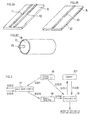
- FIG. 2 is a perspective view illustrating an example of the structure of an electrical signal communication line.
- a coplanar line shown in Fig. 2A includes a signal line 10 formed on one surface of the substrate 6, and a ground line 11 at ground potential disposed in parallel with the signal line 10 and formed so as to have the same cross-sectional area as that of the signal line 10.
- a microstrip line shown in Fig. 2B is a structure in which the signal line 10 is formed on one surface of the substrate 6 and a ground layer 12 at ground potential is formed on the other surface.
- a coaxial line shown in Fig. 2C is a structure in which an internal conductor (signal line) 15 is provided at the center of a cylindrical line, an external conductor 13 is provided at the periphery of the cylindrical line, and the space between the internal conductor 15 and external conductor 13 is filled with a dielectric 14.
- Fig. 3 is a block diagram illustrating an example of the configuration of a portion of the microcomputer module 3 that relates to the sending and receiving of signals and to computation.
- the microcomputer module 3 shown in Fig. 3 includes a directional coupler 17, a signal generator (signal transmitting means) 16, a. signal detector (reflected-wave detecting means) 18, a computing unit (computing means) 19 and a memory (storage means) 20.
- TDR Time Domain Reflectometry
- the microcomputer module 3 detects a position at which there is an impedance mismatch in the coplanar line 5, thereby specifying an entered instruction.
- the signal transmitter 16 outputs a signal while varying the frequency from 30 kHz to 3 GHz, by way of example. Further, the signal transmitter 16 outputs transmit-signal strength information, which indicates the strength of the output signal, to the computing unit 19.
- the directional coupler 17 outputs the signal, which has been output by the signal transmitter 16, to the coplanar line 5, and outputs the reflected wave, which has been output from the coplanar line 5, to the signal detector 18.
- the signal detector 18 detects the reflected wave that has been output by the directional coupler 17 and outputs received-signal strength information, which is information indicating the signal strength of the signal included in the reflected wave, to the computing unit 19.
- received-signal strength information which is information indicating the signal strength of the signal included in the reflected wave
- the computing unit 19 computes frequency-domain reflection coefficient and subjects the computed frequency-domain reflection coefficient to an inverse Fourier transform to thereby compute time-domain reflection coefficient.
- frequency-domain reflection coefficient is the ratio of signal strength of the signal included in the reflected wave to signal strength of the signal of each frequency that is output by the signal transmitter 16.
- time-domain reflection coefficient is the rate of change in the reflected wave of the signal output by the signal transmitter 16 with respect to time.
- the memory 20 stores the TDR waveform in a case where there is no impedance mismatch. Further, the memory 20 stores a key map that correlates time from the moment the signal transmitter 16 outputs a signal to the moment an impedance mismatch occurs (namely time it takes for the impedance of the coplanar line 5 to change); distance, which corresponds to this time, from the directional coupler 17 of the microcomputer module 3 to the position at which the impedance mismatch occurred; and the key corresponding to this distance.
- Fig. 4 is an explanatory view illustrating a TDR waveform in a case where an impedance mismatch has not occurred in the coplanar line 5. If an impedance mismatch has not occurred in the coplanar line 5, a reflected wave of the signal that has been output by the signal transmitter 16 is not produced. If time is plotted along the horizontal axis and impedance along the vertical axis, therefore, as illustrated in Fig. 4 , then a flat TDR waveform is obtained.
- Fig. 5 is an explanatory view illustrating a change in impedance of the coplanar line 5.
- Fig. 6 is an explanatory view illustrating an example of a key map stored by the memory 20.
- impedance changes 2t seconds after the signal transmitter 16 outputs a signal an impedance mismatch occurs at a position whose distance from the microcomputer module 3 is 21 and a "1" key corresponds to this position.
- the characteristic impedance of the coplanar line 5 is decided by the width and thickness of the signal line 10 and ground line 11.
- the signal line 10 and ground line 11 that construct the coplanar line 5 are each formed by a single line in order to make the characteristic impedance uniform. Further, the coplanar line 5 is formed on the substrate 6 in bent fashion taking into consideration the resolution of TDR.
- the path formed by the coplanar line 5 on the substrate 6 will now be described.
- the distance between keys on an ordinary portable terminal is on the order of 10 mm.
- the resolution of TDR must be made less than 10 mm.
- the resolution of TDR is one-fourth of the wavelength of the signal having the highest frequency among signals that are output by the signal transmitter 16. Accordingly, the signal transmitter 16 must output a signal having a frequency of 7.5 GHz.
- the signal may radiate from the coplanar line 5.
- the path of the coplanar line 5 on the substrate 6 is formed in bent fashion to lengthen the distance between keys artificially.
- the coplanar line 5 is formed to have bent portions in order to lengthen the distance between the portions that pass through the vicinity of each of the keys in the key sheet 1.
- Fig. 7 is an explanatory view illustrating the cross section of the substrate 6 and key sheet 1.
- the signal line 10 and ground line 11 are formed on the surface of the substrate 6 that faces the key sheet 1.
- the widths and heights of the conductor portions of the signal line 10 and ground line 11 are uniform. It should be noted that the widths and heights of the conductor portions of the signal line 10 and ground line 11 and the cross-sectional shape of the key sheet 1 in the vicinity of the signal line 10 are set in such a manner that the characteristic impedance of the coplanar line 5 (see Fig. 1 ) will be the same at any portion whatsoever. In other words, if the key sheet 1 is not pressed, an impedance mismatch is not produced in the coplanar line 5 comprising the signal line 10 and ground line 11.
- Fig. 8 is an explanatory view illustrating a cross section of the sheet key 1 that is being pressed.
- the key sheet 1 which is a dielectric
- the coplanar line 5 (see Fig. 1 ) comprising the signal line 10 and ground line 11 so that dielectric constant at the periphery of the signal line changes.
- An impedance mismatch is produced in the coplanar line as a result.
- a reflected wave of the signal that has been output by the microcomputer module 3 (see Fig. 1 ) is produced at the position on the coplanar line 5 where the impedance mismatch is produced.
- the reflected wave of the signal that has been output by the microcomputer module 3 advances toward the microcomputer module 3 through the coplanar line 5.
- the signal transmitter 16 varies frequency continuously from low frequency (e.g., 30 kHz) to high frequency (e.g., 3 GHz) and outputs a signal at all times (step S101).
- the signal transmitter 16 outputs transmit-signal strength information, which indicates the strength of the output signal, to the computing unit 19 (step S102).
- the directional coupler 17 outputs the signal, which has been output by the signal transmitter 16, to the coplanar line 5 (step S103. If an impedance mismatch has been produced in the coplanar line 5 (see Fig. 1 ), a reflected wave is output from the coplanar line 5 to the directional coupler 17 (step S104).
- the directional coupler 17 outputs the output reflected wave to the signal detector 18 (step S105).
- the signal detector 18 detects the reflected wave that has been output by the directional coupler 17 and outputs received-signal strength information, which is information indicating the signal strength of the signal included in the reflected wave, to the computing unit 19 (step S106).
- the computing unit 19 of Fig. 3 computes frequency-domain reflection coefficient based upon the transmit-signal strength information output by the signal transmitter 16 and received-signal strength information output by the signal detector 18.
- the computing unit 19 subjects the computed frequency-domain reflection coefficient to an inverse Fourier transform and obtains the result of TDR (the TDR waveform).
- a reflected wave of the signal that has been output by the signal transmitter 16 is produced. If time is plotted along the horizontal axis and impedance along the vertical axis, therefore, as illustrated in Fig. 5 , then a TDR waveform indicating a change in impedance is obtained.
- the time it takes for the TDR waveform of Fig. 5 to indicate a changes in impedance is proportional to the distance between the position at which impedance mismatch occurred and the directional coupler 17 of the microcomputer module 3. Therefore, by referring to the key map stored in the memory 20 exemplified in Fig. 6 , the computing unit 19 is capable of discriminating which key has been pressed based upon the time it takes for the TDR waveform to indicate a change in impedance (steps S107, S108 shown in Fig. 3 ).
- the computing unit 19 specifies the entered instruction based upon the result of discrimination.
- the computing unit 19 outputs information indicating the instruction (key) specified and entered (pressed) to control means of a portable terminal or the like on which the input apparatus has been mounted.
- the key input apparatus is constructed by the substrate 6, on which the coplanar line 5 has been formed, and the flexible key sheet 1. Accordingly, dome-shaped recesses of the kind shown in Fig. 11 are unnecessary. This makes it possible to reduce the thickness of the key input apparatus.
- which key has been pressed is determined based upon a change in the impedance of the coplanar line 5 formed on the substrate 6. This makes it unnecessary to provide another device or the like below the keys and makes it possible to reduce the thickness of the key input apparatus.
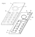
- FIG. 9 is a perspective view illustrating the key input apparatus in a case were, instead of the key sheet 1, film 23 on which key positions have been indicated has been placed on the surface of the substrate 6 on which the coplanar line 5 has been formed.
- the film 23 on which the key positions have been indicated is placed on the surface of the substrate 6 on which the coplanar line 5 has been formed, a greater reduction in the thickness of the key input apparatus can be achieved in comparison with the case where the key sheet 1 is used. It is desired that the film 23 have a high durability.
- the coplanar line 5 may have a portion 22 formed into a circle.
- Fig. 10 is a perspective view illustrating a key input apparatus in which a portion of the coplanar line 5 has been formed into a circle. If the portion of the key sheet 1 corresponding to the portion 22 of the coplanar line 5 formed into a circle is traced with a finger, then an impedance mismatch is produced at the portion traced. The position at which the impedance mismatch is produced changes depending upon the motion of the finger. Consequently, if the microcomputer module 3 discriminates motion of the finger based upon a change in the position at the impedance mismatch occurred, then the key input apparatus can be equipped with a disk-shaped operating portion.
- discrimination by the computing unit (computing means) 19 of an operated operating position based upon a reflected wave detected by the signal detector (reflected-wave detecting means) 18 means that the computing unit 19 measures the time it takes for the signal detector 18 to detect a reflected wave and computes the distance between the signal detector 18 and the operated operating position based upon the measured time, thereby discriminating the operated operating position.
- the discrimination by the computing unit 19 of an operated operating position based upon the signal strength of the signal output by the signal generator (signal transmitting means) 16 and the signal strength of the reflected wave detected by the signal detector (reflected-wave detecting means) 18 means that the computing unit 19 compares the signal strength of the signal output by the signal transmitter 16 and the signal strength of the reflected wave detected by the signal detector (reflected-wave detecting means) 18, determines that the signal detector 18 has detected a reflected wave at a timing at which the signal detector 18 has detected a signal having a signal strength different from a signal strength of the signal which has been output by the signal transmitter 16, and computes the distance between the signal detector 18 and the operating position where the operation has been done based upon the time it takes for the signal detector 18 to detect the reflected wave, thereby discriminating the operating position where the operation has been done.
- Carrying out measurement of time domain reflection coefficient by the computing unit 19 based upon the signal strength of the signal that has been output by the signal transmitter 16 and the signal strength of the reflected wave detected by the signal detector 18 means that the computing unit 19 compares the signal strength of the signal that has been output by the signal transmitter 16 as frequency is changed and the signal strength of the signal of each frequency included in the reflected wave detected by the signal detector 18, computes the frequency-domain reflection coefficient, subjects the computed frequency-domain reflection coefficient to an inverse Fourier transform and carries out time domain reflection coefficient.
- the discrimination by the computing unit 19 of an operated operating position based upon the TDR result, namely the result of measurement of the time domain reflection coefficient, means that the computing unit 19 computes the distance between the signal detector 18 and the operated operating position based upon the timing at which the time-domain reflection coefficient changes, thereby discriminating the operated operating position.
- the identification by the computing unit 19 of an entered instruction based upon the table stored by the storage means and the TDR result means that the computing unit 19 refers to the table correlating timings at which time-domain reflection coefficient changed and entered instructions and determines that an instruction corresponding to a timing at which time-domain reflection coefficient changed is an entered instruction.
- the present invention can be utilized in an input apparatus of a portable terminal or the like.
Abstract
Description
- This invention relates to a thin-type input apparatus and to an input method.
-
Fig. 11 is an explanatory view illustrating the configuration of a key portion at a conventional operating portion used in a portable terminal. A top view of the conventional key portion is illustrated inFig. 11A , and a sectional view of the conventional key portion is illustrated inFig. 11B . - The key portion illustrated in
Fig. 11 includes a flexible key sheet placed in electrical insulation relative to asubstrate 6 and having a recess with respect to thesubstrate 6, and a metal plate 9 secured in the recess as by an adhesive sheet or the like. - Further, as illustrated in
Fig. 11B , the edge of the metal plate 9 is in contact with apad face 7 formed on thesubstrate 6, and the central portion of the metal plate 9 is disposed so as to be displaceable in directions toward and away from thesubstrate 6. When the central portion of the metal plate 9 is pressed toward thesubstrate 6, the central portion of the metal plate 9 contacts apad face 8 formed on thesubstrate 6. Fin. 12 is an explanatory view illustrating the central portion of the metal plate 9 in the pressed state. - When the metal plate 9 conducts electricity owing to contact with the
pad face 8, a controller of the portable terminal detects the fact that the key portion has been pressed. -
Patent Document 1 describes a switch in which a piezoelectric element is provided on one surface of a substrate. Ultrasonic waves within the substrate that change if a finger touches the other surface of the substrate are detected, whereby contact with the finger is detected. - [Patent Document 1] Japanese Patent Application Laid-Open No.
7-282699 Fig. 1 ). - Reductions in the thickness of portable terminals have been accompanied by the pursuit for a reduction in thickness of the key portions inclusive of a plurality of keys. However, with the structure of the conventional key portion illustrated in
Figs. 11 and 12 , a gap must be provided between the central portion of the metal plate 9 and thepad face 8 so that the metal plate 9 and pad face will not conduct electrically in a state in which the key is not being pressed. As a consequence, it is difficult to reduce the thickness of the operating portion. The result is that a reduction in the thickness of the portable terminal is impeded. - Furthermore, in order to prevent faulty contact between the central portion of the metal plate 9 and the
pad face 8, it is preferred to adopt an arrangement in which foreign matter and water will not penetrate into the gap between the central portion of the metal plate 9 and thepad face 8. In order to so arrange it that foreign matter or the like will not penetrate into the gap, the key assembly process is performed in a clean room or the key portion must be constructed in such a manner that foreign matter will not penetrate into the gap after shipping. - Further, when the metal plate 9 is reduced in thickness in order to reduce the thickness of the key portion, a problem which arises is that the strength of the metal plate 9 declines, leading to the danger of destruction.
- Furthermore, since the piezoelectric element is provided on one surface of the substrate in the switch described in
Patent Document 1, it is difficult to achieve a reduction in thickness. - Accordingly, a main object of the present invention is to provide an input apparatus and method that enable a reduction in thickness and prevention of the occurrence of contact failure.
- According to the present invention, there is provided an input apparatus including a substrate on a surface of which a signal line has been formed, and an insulating sheet disposed facing the surface of the substrate and having information, which represents a plurality of operating positions, indicated on a surface thereof that is opposite surface facing the substrate, characterized in that the apparatus comprises: signal transmitting means for outputting a signal to the signal line; reflected-wave detecting means for detecting a reflected wave of the signal that has been output by the signal transmitting means; and computing means for discriminating an operating position at which an operation has been performed, based upon the reflected wave detected by the reflected-wave detecting means.
- In the present invention, the signal line may be formed so as to pass through the vicinity of the operating positions in the insulating sheet, and a ground line at ground potential may be formed on the substrate in parallel with the signal line.
- In the present invention, the signal line may be formed so as to lengthen distance between a portion that passes through the vicinity of an operating position in the insulating sheet and a portion that passes through the vicinity of another operating position.
- In the present invention, the computing means may discriminate an operating position at which an operation has been performed, based upon signal strength of the signal that has been output by the signal transmitting means and signal strength of the reflected wave detected by the reflected-wave detecting means.
- In the present invention, the computing means may perform time domain reflectometry based upon signal strength of the signal that has been output by the signal transmitting means and signal strength of the reflected wave detected by the reflected-wave detecting means, and may discriminate an operating position at which an operation has been performed, based upon result of time domain reflectometry.
- In the present invention, the input apparatus may further comprise storage means in which a table correlating the result of time domain reflectometry (TDR) and entered instructions has been stored in advance, wherein the computing means specifies an entered instruction based upon the table stored by the storage means and the result of TDR.
- In the present invention, the signal line may be formed on the substrate so as to have a circular portion, and the computing means may discriminate an operation that has been performed on the insulating sheet, based upon a change in the result of TDR.
- According to the present invention, three is provided an input method which uses an input apparatus having a substrate on a surface of which a signal line has been formed, and an insulating sheet disposed facing the surface of the substrate and having information, which represents a plurality of operating positions, indicated on a surface thereof that is on a side opposite a surface facing the substrate, characterized in that the method comprises: a signal output step of signal transmitting means outputting a signal to the signal line; a reflected-wave detecting step of reflected-wave detecting means detecting a reflected wave of the signal that has been output by the signal transmitting means at the signal outputs step; and a computing step of computing means discriminating an operating position at which an operation has been performed, based upon the reflected wave detected by the reflected-wave detecting means at the reflected-wave detecting step.
- In accordance with the present invention, it is possible to prevent the occurrence of contact failure and to achieve a reduction in thickness. The reason for this is that in the present invention, the input apparatus does not have a mechanical switch structure and, as a result, the input apparatus can be reduced in thickness and it is possible to prevent the occurrence of contact failure due to entry of foreign matter, etc.
- In a case where the signal line and the ground line have been formed on the substrate in parallel so as to pass through the vicinity of an operating position in the present invention, a coplanar line is constructed. If the finger of a user touches the operating position, therefore, a reflected wave of the signal that has been output by the signal transmitting means is produced and the reflected-wave detecting means can detect this reflected wave.
- In a case where the signal line has been formed so as to lengthen distance between a portion that passes through the vicinity of an operating position in the insulating sheet and a portion that passes through the vicinity of another operating position in the present invention, the distance between the operating positions can be lengthened artificially to thereby enable lowering of the frequency of the signal that is output by the signal transmitting means.
- In a case where the signal line is formed on the substrate so as to have a circular portion and it is so arranged that the computing means specifies an entered instruction based upon a change in the result of TDR in the present invention, the input apparatus is capable of accommodating input of an instruction that conforms to movement of the finger of a user.
-
-
Fig. 1 is a perspective view illustrating an example of the configuration of a key input apparatus according to an embodiment of the present invention; -
Fig. 2 is a perspective view illustrating an example of the structure of an electrical signal communication line; -
Fig. 3 is a block diagram illustrating an example of arrangement of microcomputer modules; -
Fig. 4 is an explanatory view illustrating a TDR waveform in a case where an impedance mismatch has not occurred in a coplanar line; -
Fig. 5 is an explanatory view illustrating a change in impedance; -
Fig. 6 is an explanatory view illustrating an example of a key map stored by a memory; -
Fig. 7 is an explanatory view illustrating a cross section of a substrate and key sheet; -
Fig. 8 is an explanatory view illustrating a cross section of a sheet key that is being pressed; -
Fig. 9 is a perspective view illustrating a key input apparatus in which a film has been placed; -
Fig. 10 is a perspective view illustrating a key input apparatus in which a portion of a coplanar line has been formed into a circle; -
Fig. 11 is an explanatory view illustrating the configuration of a conventional key portion used in a portable terminal; and -
Fig. 12 is an explanatory view illustrating the central portion of a metal plate in a pressed state. -
- 1
- key sheet
- 2
- key position
- 3
- microcomputer module
- 4
- terminating resistor
- 5
- coplanar line
- 6
- substrate
- 7, 8
- pad face
- 9
- metal plate
- 10
- signal line
- 11
- ground line
- 12
- ground layer
- 13
- external conductor
- 14
- dielectric
- 15
- internal conductor
- 16
- signal generator
- 17
- directional coupler
- 18
- signal detector
- 19
- computing unit
- 20
- memory
- 21
- interface line
- 22
- portion formed into circle
- 23
- film
- Exemplary embodiments of the present invention will be described with reference to the drawings.
Fig. 1 is a perspective view illustrating an example of the configuration of a key input apparatus (input apparatus) according to an exemplary embodiment of the present invention. - The key input apparatus shown in
Fig. 1 includes an elastic key sheet (insulating sheet) 1, the main ingredient of which is silicone rubber or the like, and asubstrate 6 on which a coplanar line 5 has been formed. - In a case where the
key sheet 1 is applied to numeric keys, numerals and the like are printed on one surface of thekey sheet 1 and recesses of a conical or cylindrical shape are provided at portions on the other surface that correspond to the numerals, etc., printed on the first-mentioned surface. In other words, the positions of the recesses provided in one surface of thekey sheet 1 correspond topositions 2 of keys of the numerals, etc., printed on thekey sheet 1. - A terminating
resistor 4 is placed at one end of the coplanar line 5 onsubstrate 6, and amicrocomputer nodule 3 is placed at the other end of the coplanar line. The coplanar line 5 is formed so as to pass through the vicinity of each key of the numerals, etc., printed on thekey sheet 1.interface lines 21 are formed on thesubstrate 6 for connecting themicrocomputer module 3 and other modules, etc. -
Fig. 2 is a perspective view illustrating an example of the structure of an electrical signal communication line. A coplanar line shown inFig. 2A includes asignal line 10 formed on one surface of thesubstrate 6, and aground line 11 at ground potential disposed in parallel with thesignal line 10 and formed so as to have the same cross-sectional area as that of thesignal line 10. - A microstrip line shown in
Fig. 2B is a structure in which thesignal line 10 is formed on one surface of thesubstrate 6 and aground layer 12 at ground potential is formed on the other surface. - A coaxial line shown in
Fig. 2C is a structure in which an internal conductor (signal line) 15 is provided at the center of a cylindrical line, anexternal conductor 13 is provided at the periphery of the cylindrical line, and the space between theinternal conductor 15 andexternal conductor 13 is filled with a dielectric 14. -
Fig. 3 is a block diagram illustrating an example of the configuration of a portion of themicrocomputer module 3 that relates to the sending and receiving of signals and to computation. Themicrocomputer module 3 shown inFig. 3 includes adirectional coupler 17, a signal generator (signal transmitting means) 16, a. signal detector (reflected-wave detecting means) 18, a computing unit (computing means) 19 and a memory (storage means) 20. Using TDR (Time Domain Reflectometry), which is means for directly measuring reflected waves in time domain, themicrocomputer module 3 detects a position at which there is an impedance mismatch in the coplanar line 5, thereby specifying an entered instruction. - The
signal transmitter 16 outputs a signal while varying the frequency from 30 kHz to 3 GHz, by way of example. Further, thesignal transmitter 16 outputs transmit-signal strength information, which indicates the strength of the output signal, to thecomputing unit 19. Thedirectional coupler 17 outputs the signal, which has been output by thesignal transmitter 16, to the coplanar line 5, and outputs the reflected wave, which has been output from the coplanar line 5, to thesignal detector 18. - The
signal detector 18 detects the reflected wave that has been output by thedirectional coupler 17 and outputs received-signal strength information, which is information indicating the signal strength of the signal included in the reflected wave, to thecomputing unit 19. On the basis of the transmit-signal strength information and received-signal strength information, thecomputing unit 19 computes frequency-domain reflection coefficient and subjects the computed frequency-domain reflection coefficient to an inverse Fourier transform to thereby compute time-domain reflection coefficient. It should be noted that frequency-domain reflection coefficient is the ratio of signal strength of the signal included in the reflected wave to signal strength of the signal of each frequency that is output by thesignal transmitter 16. Further, time-domain reflection coefficient is the rate of change in the reflected wave of the signal output by thesignal transmitter 16 with respect to time. - In order to measure a position at which there is an impedance mismatch in the coplanar line 5 based upon time-domain reflection coefficient, the
memory 20 stores the TDR waveform in a case where there is no impedance mismatch. Further, thememory 20 stores a key map that correlates time from the moment thesignal transmitter 16 outputs a signal to the moment an impedance mismatch occurs (namely time it takes for the impedance of the coplanar line 5 to change); distance, which corresponds to this time, from thedirectional coupler 17 of themicrocomputer module 3 to the position at which the impedance mismatch occurred; and the key corresponding to this distance. -
Fig. 4 is an explanatory view illustrating a TDR waveform in a case where an impedance mismatch has not occurred in the coplanar line 5. If an impedance mismatch has not occurred in the coplanar line 5, a reflected wave of the signal that has been output by thesignal transmitter 16 is not produced. If time is plotted along the horizontal axis and impedance along the vertical axis, therefore, as illustrated inFig. 4 , then a flat TDR waveform is obtained. -
Fig. 5 is an explanatory view illustrating a change in impedance of the coplanar line 5. In the example shown inFig. 5 , it is shown that impedance changes L seconds after thesignal transmitter 16 outputs a signal.Fig. 6 is an explanatory view illustrating an example of a key map stored by thememory 20. In the example shown inFig. 6 , it is illustrated that in a case whereimpedance changes 2t seconds after thesignal transmitter 16 outputs a signal, an impedance mismatch occurs at a position whose distance from themicrocomputer module 3 is 21 and a "1" key corresponds to this position. - The characteristic impedance of the coplanar line 5 is decided by the width and thickness of the
signal line 10 andground line 11. Thesignal line 10 andground line 11 that construct the coplanar line 5 are each formed by a single line in order to make the characteristic impedance uniform. Further, the coplanar line 5 is formed on thesubstrate 6 in bent fashion taking into consideration the resolution of TDR. - The path formed by the coplanar line 5 on the
substrate 6 will now be described. The distance between keys on an ordinary portable terminal is on the order of 10 mm. In order to mount the key input apparatus on a portable terminal, therefore, the resolution of TDR must be made less than 10 mm. Further, it is assumed that the resolution of TDR is one-fourth of the wavelength of the signal having the highest frequency among signals that are output by thesignal transmitter 16. Accordingly, thesignal transmitter 16 must output a signal having a frequency of 7.5 GHz. - However, since a high-frequency signal exhibits strong rectilinear propagation property, the signal may radiate from the coplanar line 5. In order to lower the frequency of the signal that is output by the
signal transmitter 16, the path of the coplanar line 5 on thesubstrate 6 is formed in bent fashion to lengthen the distance between keys artificially. In other words, the coplanar line 5 is formed to have bent portions in order to lengthen the distance between the portions that pass through the vicinity of each of the keys in thekey sheet 1. -
Fig. 7 is an explanatory view illustrating the cross section of thesubstrate 6 andkey sheet 1. Thesignal line 10 andground line 11 are formed on the surface of thesubstrate 6 that faces thekey sheet 1. The widths and heights of the conductor portions of thesignal line 10 andground line 11 are uniform. It should be noted that the widths and heights of the conductor portions of thesignal line 10 andground line 11 and the cross-sectional shape of thekey sheet 1 in the vicinity of thesignal line 10 are set in such a manner that the characteristic impedance of the coplanar line 5 (seeFig. 1 ) will be the same at any portion whatsoever. In other words, if thekey sheet 1 is not pressed, an impedance mismatch is not produced in the coplanar line 5 comprising thesignal line 10 andground line 11. That is, in relation to the coplanar line comprising thesignal line 10 andground line 11 wired on the surface of thesubstrate 6 so as to pass through the recesses provided in the side of thekey sheet 1 that faces thesubstrate 6, a gap exists between thekey sheet 1 and the opposing surface of the substrate in a state in which thekey sheet 1 is not being pressed, as illustrated inFig. 7 . - In the example illustrated in
Fig. 7 , an impedance mismatch is not produced in the coplanar line 5 because thekey sheet 1 is not being pressed. Consequently, the signal that has been output by thesignal transmitter 16 is consumed by the terminatingresistor 4 and a reflected wave is not produced. -
Fig. 8 is an explanatory view illustrating a cross section of thesheet key 1 that is being pressed. When thekey sheet 1 is pressed, as shown inFig. 8 , thekey sheet 1, which is a dielectric, is deformed (flexed) and comes into contact with the coplanar line 5 (seeFig. 1 ) comprising thesignal line 10 andground line 11 so that dielectric constant at the periphery of the signal line changes. An impedance mismatch is produced in the coplanar line as a result. A reflected wave of the signal that has been output by the microcomputer module 3 (seeFig. 1 ) is produced at the position on the coplanar line 5 where the impedance mismatch is produced. The reflected wave of the signal that has been output by themicrocomputer module 3 advances toward themicrocomputer module 3 through the coplanar line 5. - Next, the operation of the
microcomputer module 3 ofFig. 1 will be described with reference toFig. 3 . Thesignal transmitter 16 varies frequency continuously from low frequency (e.g., 30 kHz) to high frequency (e.g., 3 GHz) and outputs a signal at all times (step S101). Thesignal transmitter 16 outputs transmit-signal strength information, which indicates the strength of the output signal, to the computing unit 19 (step S102). - The
directional coupler 17 outputs the signal, which has been output by thesignal transmitter 16, to the coplanar line 5 (step S103. If an impedance mismatch has been produced in the coplanar line 5 (seeFig. 1 ), a reflected wave is output from the coplanar line 5 to the directional coupler 17 (step S104). Thedirectional coupler 17 outputs the output reflected wave to the signal detector 18 (step S105). Thesignal detector 18 detects the reflected wave that has been output by thedirectional coupler 17 and outputs received-signal strength information, which is information indicating the signal strength of the signal included in the reflected wave, to the computing unit 19 (step S106). - The
computing unit 19 ofFig. 3 computes frequency-domain reflection coefficient based upon the transmit-signal strength information output by thesignal transmitter 16 and received-signal strength information output by thesignal detector 18. Thecomputing unit 19 subjects the computed frequency-domain reflection coefficient to an inverse Fourier transform and obtains the result of TDR (the TDR waveform). - If an impedance mismatch is produced in the coplanar line 5, a reflected wave of the signal that has been output by the
signal transmitter 16 is produced. If time is plotted along the horizontal axis and impedance along the vertical axis, therefore, as illustrated inFig. 5 , then a TDR waveform indicating a change in impedance is obtained. - The time it takes for the TDR waveform of
Fig. 5 to indicate a changes in impedance is proportional to the distance between the position at which impedance mismatch occurred and thedirectional coupler 17 of themicrocomputer module 3. Therefore, by referring to the key map stored in thememory 20 exemplified inFig. 6 , thecomputing unit 19 is capable of discriminating which key has been pressed based upon the time it takes for the TDR waveform to indicate a change in impedance (steps S107, S108 shown inFig. 3 ). - The
computing unit 19 specifies the entered instruction based upon the result of discrimination. Thecomputing unit 19 outputs information indicating the instruction (key) specified and entered (pressed) to control means of a portable terminal or the like on which the input apparatus has been mounted. - In accordance with this exemplary embodiment, the key input apparatus is constructed by the
substrate 6, on which the coplanar line 5 has been formed, and the flexiblekey sheet 1. Accordingly, dome-shaped recesses of the kind shown inFig. 11 are unnecessary. This makes it possible to reduce the thickness of the key input apparatus. - Further, in accordance with this exemplary embodiment, which key has been pressed is determined based upon a change in the impedance of the coplanar line 5 formed on the
substrate 6. This makes it unnecessary to provide another device or the like below the keys and makes it possible to reduce the thickness of the key input apparatus. - Further, in accordance with this exemplary embodiment, mechanical switches do not exist between the coplanar line 5 formed on the
substrate 6 and thekey sheet 1. The effect obtained is that the key input apparatus does not experience deterioration and malfunction due to mechanical wear. Further, even if foreign matter and water, etc., penetrate into the space between the coplanar line 5 formed on thesubstrate 6 and thekey sheet 1, malfunction such as contact failure will not occur. - It should be noted that instead of the
key sheet 1, an insulatingfilm 23 on which key positions have been indicated may be placed on the surface of thesubstrate 6 on which the coplanar line 5 has been formed.Fig. 9 is a perspective view illustrating the key input apparatus in a case were, instead of thekey sheet 1,film 23 on which key positions have been indicated has been placed on the surface of thesubstrate 6 on which the coplanar line 5 has been formed. - In this case also in which the
film 23 has been placed on the surface of thesubstrate 6 on which the coplanar line 5 has been formed, when thefilm 23 is touched by a finger or the like, the dielectric constant at the periphery of the position touched by the finger or the like changes and an impedance mismatch is produced. Consequently, a reflected wave is produced at the position of the coplanar line 5 touched by the finger or the like and themicrocomputer module 3 obtains the TDR waveform based upon the reflected wave and can discriminate which key was touched by the finger, etc. - In a case where the
film 23 on which the key positions have been indicated is placed on the surface of thesubstrate 6 on which the coplanar line 5 has been formed, a greater reduction in the thickness of the key input apparatus can be achieved in comparison with the case where thekey sheet 1 is used. It is desired that thefilm 23 have a high durability. - Further, the coplanar line 5 may have a
portion 22 formed into a circle.Fig. 10 is a perspective view illustrating a key input apparatus in which a portion of the coplanar line 5 has been formed into a circle. If the portion of thekey sheet 1 corresponding to theportion 22 of the coplanar line 5 formed into a circle is traced with a finger, then an impedance mismatch is produced at the portion traced. The position at which the impedance mismatch is produced changes depending upon the motion of the finger. Consequently, if themicrocomputer module 3 discriminates motion of the finger based upon a change in the position at the impedance mismatch occurred, then the key input apparatus can be equipped with a disk-shaped operating portion. - It should be noted that discrimination by the computing unit (computing means) 19 of an operated operating position based upon a reflected wave detected by the signal detector (reflected-wave detecting means) 18 means that the
computing unit 19 measures the time it takes for thesignal detector 18 to detect a reflected wave and computes the distance between thesignal detector 18 and the operated operating position based upon the measured time, thereby discriminating the operated operating position. - The discrimination by the
computing unit 19 of an operated operating position based upon the signal strength of the signal output by the signal generator (signal transmitting means) 16 and the signal strength of the reflected wave detected by the signal detector (reflected-wave detecting means) 18 means that thecomputing unit 19 compares the signal strength of the signal output by thesignal transmitter 16 and the signal strength of the reflected wave detected by the signal detector (reflected-wave detecting means) 18, determines that thesignal detector 18 has detected a reflected wave at a timing at which thesignal detector 18 has detected a signal having a signal strength different from a signal strength of the signal which has been output by thesignal transmitter 16, and computes the distance between thesignal detector 18 and the operating position where the operation has been done based upon the time it takes for thesignal detector 18 to detect the reflected wave, thereby discriminating the operating position where the operation has been done. - Carrying out measurement of time domain reflection coefficient by the
computing unit 19 based upon the signal strength of the signal that has been output by thesignal transmitter 16 and the signal strength of the reflected wave detected by thesignal detector 18 means that thecomputing unit 19 compares the signal strength of the signal that has been output by thesignal transmitter 16 as frequency is changed and the signal strength of the signal of each frequency included in the reflected wave detected by thesignal detector 18, computes the frequency-domain reflection coefficient, subjects the computed frequency-domain reflection coefficient to an inverse Fourier transform and carries out time domain reflection coefficient. - The discrimination by the
computing unit 19 of an operated operating position based upon the TDR result, namely the result of measurement of the time domain reflection coefficient, means that thecomputing unit 19 computes the distance between thesignal detector 18 and the operated operating position based upon the timing at which the time-domain reflection coefficient changes, thereby discriminating the operated operating position. - The identification by the
computing unit 19 of an entered instruction based upon the table stored by the storage means and the TDR result means that thecomputing unit 19 refers to the table correlating timings at which time-domain reflection coefficient changed and entered instructions and determines that an instruction corresponding to a timing at which time-domain reflection coefficient changed is an entered instruction. - The present invention can be utilized in an input apparatus of a portable terminal or the like.
Claims (13)
- An input apparatus which comprises a substrate on a surface of which a signal line is formed, and an insulating sheet disposed facing the surface of the substrate and having information, which represents a plurality of operating positions, displayed on a surface thereof that is on a side opposite a surface facing the substrate, the apparatus comprising:signal transmitting means for outputting a signal to the signal line;reflected-wave detecting means for detecting a reflected wave of the signal output by the signal transmitting means; andcomputing means for discriminating an operating position at which an operation has been performed, based upon the reflected wave detected by the reflected-wave detecting means.
- The input apparatus according to claim 1, wherein the signal line is formed so as to pass through the vicinity of the operating positions in the insulating sheet, and a ground line at ground potential is formed on the substrate in parallel with the signal line.
- The input apparatus according to claim 1 or 2, wherein the signal line is formed so as to lengthen distance between a portion that passes through the vicinity of an operating position in the insulating sheet and a portion that passes through the vicinity of another operating position.
- The input apparatus according to claim 1 or 2, wherein the computing means discriminates an operating position at which an operation has been performed, based upon signal strength of the signal output by the signal transmitting means and signal strength of the reflected wave detected by the reflected-wave detecting means.
- The input apparatus according to claim 1 or 2, wherein the computing means performs measuring time domain reflection coefficient based upon signal strength of the signal output by the signal transmitting means and signal strength of the reflected wave detected by the reflected-wave detecting means, and discriminates an operating position at which an operation has been performed, based upon result of TDR which is the result of the measurement of time domain reflection coefficient.
- The input apparatus according to claim 5, further comprising storage means in which a table correlating the result of TDR and entered instructions is stored in advance;
wherein the computing means specifies an entered instruction based upon the table stored by the storage means and the result of TDR. - The input apparatus according to claim 5 or 6, wherein the signal line is formed on the substrate so as to have a circular portion; and
the computing means discriminates an operation that has been performed on the insulating sheet, based upon a change in the result. - An input method using an input apparatus comprising a substrate on a surface of which a signal line has been formed, and an insulating sheet disposed facing the surface of the substrate and having information, which represents a plurality of operating positions, displayed on a surface thereof that is on a side opposite a surface facing the substrate, the method comprising:a signal output step of signal transmitting means outputting a signal to the signal line;a reflected-wave detecting step of reflected-wave detecting means detecting a reflected wave of the signal output by the signal transmitting means at the signal output step; anda computing step of computing means discriminating an operating position at which an operation has been performed, based upon the reflected wave detected by the reflected-wave detecting means at the reflected-wave detecting step.
- An input apparatus comprising:an insulating member having keys assigned to predetermined prescribed portions thereof;a substrate having a signal line on a side thereof opposing the insulating member, the signal line being wired so as to pass through positions corresponding to the portions on the insulating member to which the keys are assigned and having one end thereof terminated; andmeans for discriminating an operated key based upon result of measuring a reflected wave, which is produced in the signal line by an impedance mismatch, when a portion on the insulating member to which a key is assigned is operated in a state in which a signal is being supplied from the other end of the signal line.
- The input apparatus according to claim 9, wherein the signal line includes a portion wired in the form of a loop, the portion corresponding to a disk-shaped key operating portion provided on the insulating member; further comprising
means for discriminating motion of a finger of an operator based upon a reflected wave produced in the signal line in accordance with motion of the finger when the disk-shaped key operating portion of the insulating member is operated by the finger of the operator in a state in which a signal is being supplied from the other end of the signal line. - The input apparatus according to claim 9, wherein the insulating member has recesses in a surface thereof facing the substrate, the recesses corresponding to positions indicating information representing operating positions on the surface of the opposite side; and
the signal line is wired so as to pass through positions corresponding to the recesses of the insulating member. - The input apparatus according to claim 9, wherein the insulating member comprises a film disposed on the substrate surface.
- The input apparatus according to claim 9, wherein the signal line has bent portions on the substrate at portions that pass through the vicinity of the portion on the insulating member to which the keys are assigned.
Applications Claiming Priority (2)
| Application Number | Priority Date | Filing Date | Title |
|---|---|---|---|
| JP2006091791 | 2006-03-29 | ||
| PCT/JP2007/056177 WO2007111291A1 (en) | 2006-03-29 | 2007-03-26 | Inputting apparatus and inputting method |
Publications (3)
| Publication Number | Publication Date |
|---|---|
| EP2000887A1 true EP2000887A1 (en) | 2008-12-10 |
| EP2000887A4 EP2000887A4 (en) | 2010-07-28 |
| EP2000887B1 EP2000887B1 (en) | 2013-07-17 |
Family
ID=38541208
Family Applications (1)
| Application Number | Title | Priority Date | Filing Date |
|---|---|---|---|
| EP07739615.8A Expired - Fee Related EP2000887B1 (en) | 2006-03-29 | 2007-03-26 | Inputting apparatus and inputting method |
Country Status (5)
| Country | Link |
|---|---|
| US (1) | US8286489B2 (en) |
| EP (1) | EP2000887B1 (en) |
| JP (1) | JP5298848B2 (en) |
| CN (1) | CN101395560B (en) |
| WO (1) | WO2007111291A1 (en) |
Cited By (2)
| Publication number | Priority date | Publication date | Assignee | Title |
|---|---|---|---|---|
| WO2011137201A3 (en) * | 2010-04-30 | 2011-12-29 | Microchip Technology Incorporated | Touch sense using time domain reflectometry |
| WO2012145268A1 (en) * | 2011-04-21 | 2012-10-26 | Microchip Technology Incorporated | Touch sense determined by characterizing impedance changes in a transmission line |
Families Citing this family (16)
| Publication number | Priority date | Publication date | Assignee | Title |
|---|---|---|---|---|
| CN102012786A (en) * | 2010-11-15 | 2011-04-13 | 中兴通讯股份有限公司 | Press key realization method, press key system and mobile terminal |
| TWI581135B (en) * | 2011-09-30 | 2017-05-01 | 加拿都公司 | Touch sensitive film, touch sensing device, and electronic device |
| US20140132523A1 (en) * | 2012-11-13 | 2014-05-15 | David Brent GUARD | Touch Sensing Based On Signal Reflections |
| US10067607B2 (en) * | 2014-01-17 | 2018-09-04 | Lg Innotek Co., Ltd. | Time domain reflectometry touch window sensor |
| KR102175668B1 (en) * | 2014-05-14 | 2020-11-06 | 엘지이노텍 주식회사 | Electronic apparatus |
| US10261631B2 (en) | 2014-05-08 | 2019-04-16 | Lg Innotek Co., Ltd. | Electronic device |
| KR102152857B1 (en) * | 2014-05-08 | 2020-09-07 | 엘지이노텍 주식회사 | Touch window |
| JP2016180747A (en) * | 2015-03-24 | 2016-10-13 | パナソニックIpマネジメント株式会社 | Pressure sensor |
| CN106383622A (en) * | 2016-09-19 | 2017-02-08 | 广州视源电子科技股份有限公司 | TDR (Time-Domain Reflectometry) scanning type touch screen, touch scanning positioning method and touch liquid crystal display screen |
| CN106406646A (en) * | 2016-09-19 | 2017-02-15 | 广州视源电子科技股份有限公司 | A TDR scanning type touch screen and a touch scanning locating method |
| CN106468974B (en) * | 2016-09-19 | 2020-03-17 | 广州视源电子科技股份有限公司 | Touch screen calibration method and touch scanning positioning method |
| CN106249962A (en) * | 2016-09-19 | 2016-12-21 | 广州视源电子科技股份有限公司 | TDR scan-type touch screen and touch-control localization method |
| CN106406649A (en) * | 2016-09-19 | 2017-02-15 | 广州视源电子科技股份有限公司 | A TDR touch screen and a touch scanning locating method |
| CN106371683A (en) * | 2016-09-19 | 2017-02-01 | 广州视源电子科技股份有限公司 | TDR touch screen and touch positioning method |
| CN106371668A (en) * | 2016-09-19 | 2017-02-01 | 广州视源电子科技股份有限公司 | Touch object shape recognition method and device and touch screen |
| CN106354330B (en) * | 2016-09-19 | 2020-07-28 | 广州视源电子科技股份有限公司 | Touch screen response method and device based on user input pressure |
Citations (2)
| Publication number | Priority date | Publication date | Assignee | Title |
|---|---|---|---|---|
| EP0483519A1 (en) * | 1990-10-29 | 1992-05-06 | International Business Machines Corporation | Touch sensitive overlay |
| US6137282A (en) * | 1998-06-25 | 2000-10-24 | Becs Technology, Inc. | Time-domain reflectometry user input device |
Family Cites Families (9)
| Publication number | Priority date | Publication date | Assignee | Title |
|---|---|---|---|---|
| JP2964667B2 (en) | 1991-03-04 | 1999-10-18 | 株式会社スリーボンド | Different material composite injection molding machine |
| JPH054254U (en) * | 1991-07-02 | 1993-01-22 | 横河電機株式会社 | Input device |
| TW241352B (en) | 1994-03-30 | 1995-02-21 | Whitaker Corp | Reflective mode ultrasonic touch sensitive switch |
| JPH11194883A (en) | 1998-01-06 | 1999-07-21 | Poseidon Technical Systems:Kk | Touch operation type computer |
| CN100374988C (en) * | 2000-09-22 | 2008-03-12 | 北京青谷科技有限公司 | Supersonic hand-writing keyboard |
| US20050088417A1 (en) * | 2003-10-24 | 2005-04-28 | Mulligan Roger C. | Tactile touch-sensing system |
| US8184108B2 (en) * | 2004-06-30 | 2012-05-22 | Poa Sana Liquidating Trust | Apparatus and method for a folded optical element waveguide for use with light based touch screens |
| US7412119B2 (en) * | 2004-06-30 | 2008-08-12 | Poa Sana Liquidating Trust | Apparatus and method for making flexible waveguide substrates for use with light based touch screens |
| KR20090007776A (en) * | 2006-05-01 | 2009-01-20 | 알피오 피티와이 리미티드 | Waveguide materials for optical touch screens |
-
2007
- 2007-03-26 JP JP2008507484A patent/JP5298848B2/en not_active Expired - Fee Related
- 2007-03-26 CN CN200780007254.4A patent/CN101395560B/en not_active Expired - Fee Related
- 2007-03-26 EP EP07739615.8A patent/EP2000887B1/en not_active Expired - Fee Related
- 2007-03-26 WO PCT/JP2007/056177 patent/WO2007111291A1/en active Application Filing
- 2007-03-26 US US12/281,199 patent/US8286489B2/en not_active Expired - Fee Related
Patent Citations (2)
| Publication number | Priority date | Publication date | Assignee | Title |
|---|---|---|---|---|
| EP0483519A1 (en) * | 1990-10-29 | 1992-05-06 | International Business Machines Corporation | Touch sensitive overlay |
| US6137282A (en) * | 1998-06-25 | 2000-10-24 | Becs Technology, Inc. | Time-domain reflectometry user input device |
Non-Patent Citations (1)
| Title |
|---|
| See also references of WO2007111291A1 * |
Cited By (5)
| Publication number | Priority date | Publication date | Assignee | Title |
|---|---|---|---|---|
| WO2011137201A3 (en) * | 2010-04-30 | 2011-12-29 | Microchip Technology Incorporated | Touch sense using time domain reflectometry |
| WO2012145268A1 (en) * | 2011-04-21 | 2012-10-26 | Microchip Technology Incorporated | Touch sense determined by characterizing impedance changes in a transmission line |
| CN103477310A (en) * | 2011-04-21 | 2013-12-25 | 密克罗奇普技术公司 | Touch sense determined by characterizing impedance changes in a transmission line |
| US8972214B2 (en) | 2011-04-21 | 2015-03-03 | Microchip Technology Incorporated | Touch sense determined by characterizing impedance changes in a transmission line |
| CN103477310B (en) * | 2011-04-21 | 2017-11-14 | 密克罗奇普技术公司 | By the way that the impedance in transmission line is changed into the touch-sensing characterized to determine |
Also Published As
| Publication number | Publication date |
|---|---|
| US20090013788A1 (en) | 2009-01-15 |
| WO2007111291A1 (en) | 2007-10-04 |
| CN101395560A (en) | 2009-03-25 |
| JPWO2007111291A1 (en) | 2009-08-13 |
| JP5298848B2 (en) | 2013-09-25 |
| EP2000887A4 (en) | 2010-07-28 |
| EP2000887B1 (en) | 2013-07-17 |
| CN101395560B (en) | 2013-07-24 |
| US8286489B2 (en) | 2012-10-16 |
Similar Documents
| Publication | Publication Date | Title |
|---|---|---|
| US8286489B2 (en) | Input apparatus and input method | |
| US10276922B2 (en) | Radiating structure with integrated proximity sensing | |
| US9886156B2 (en) | Radiofrequency-wave-transparent capacitive sensor pad | |
| EP2187226B1 (en) | Ultra-high frequency partial discharge array sensor apparatus for high-voltage power apparatus | |
| US20120162040A1 (en) | Mobile wireless terminal | |
| US20070209920A1 (en) | Keyboard and membrane switch for keyboard | |
| US20160283006A1 (en) | Pressure sensor including time-domain reflectometer | |
| US7659889B2 (en) | Touch panel device | |
| JPWO2014103316A1 (en) | Non-contact power feeding device | |
| US20110080270A1 (en) | Data input device | |
| JP2004022356A (en) | Touch switch | |
| CN115882902A (en) | Power generation or distribution asset monitoring | |
| US5923101A (en) | Non-contact key | |
| CN112398546B (en) | Electronic device | |
| CN111465915A (en) | Minimal driving of transmitter to increase hover detection | |
| CN114839509A (en) | Radio frequency test system and radio frequency test method | |
| KR20160060292A (en) | Touch sensing devices of TDR type | |
| JP5865569B2 (en) | Transmission system, transmission method, heat dissipation fan control method and electronic device mounted on electronic device | |
| KR20190077982A (en) | Radio frequency band based touch sensing apparatus and operation method of said apparatus | |
| JP4829271B2 (en) | Antenna and module for microwave detector and microwave detector | |
| JP2009237856A (en) | Touch panel device | |
| CN114425156A (en) | Press response subassembly and terminal equipment | |
| TW201904209A (en) | Electronic composite detection antenna maintaining a better power for transmitting the radio frequency signal | |
| KR20040075598A (en) | Switch device with net shaped insulator and method for producing the same | |
| JPH081378B2 (en) | Thickness measuring device |
Legal Events
| Date | Code | Title | Description |
|---|---|---|---|
| PUAI | Public reference made under article 153(3) epc to a published international application that has entered the european phase |
Free format text: ORIGINAL CODE: 0009012 |
|
| 17P | Request for examination filed |
Effective date: 20080819 |
|
| AK | Designated contracting states |
Kind code of ref document: A1 Designated state(s): DE FR GB IT |
|
| DAX | Request for extension of the european patent (deleted) | ||
| RBV | Designated contracting states (corrected) |
Designated state(s): DE FR GB IT |
|
| A4 | Supplementary search report drawn up and despatched |
Effective date: 20100628 |
|
| 17Q | First examination report despatched |
Effective date: 20100712 |
|
| GRAP | Despatch of communication of intention to grant a patent |
Free format text: ORIGINAL CODE: EPIDOSNIGR1 |
|
| GRAP | Despatch of communication of intention to grant a patent |
Free format text: ORIGINAL CODE: EPIDOSNIGR1 |
|
| GRAS | Grant fee paid |
Free format text: ORIGINAL CODE: EPIDOSNIGR3 |
|
| GRAA | (expected) grant |
Free format text: ORIGINAL CODE: 0009210 |
|
| AK | Designated contracting states |
Kind code of ref document: B1 Designated state(s): DE FR GB IT |
|
| REG | Reference to a national code |
Ref country code: GB Ref legal event code: FG4D |
|
| REG | Reference to a national code |
Ref country code: DE Ref legal event code: R096 Ref document number: 602007031702 Country of ref document: DE Effective date: 20130912 |
|
| PLBE | No opposition filed within time limit |
Free format text: ORIGINAL CODE: 0009261 |
|
| STAA | Information on the status of an ep patent application or granted ep patent |
Free format text: STATUS: NO OPPOSITION FILED WITHIN TIME LIMIT |
|
| PG25 | Lapsed in a contracting state [announced via postgrant information from national office to epo] |
Ref country code: IT Free format text: LAPSE BECAUSE OF FAILURE TO SUBMIT A TRANSLATION OF THE DESCRIPTION OR TO PAY THE FEE WITHIN THE PRESCRIBED TIME-LIMIT Effective date: 20130717 |
|
| 26N | No opposition filed |
Effective date: 20140422 |
|
| REG | Reference to a national code |
Ref country code: DE Ref legal event code: R097 Ref document number: 602007031702 Country of ref document: DE Effective date: 20140422 |
|
| REG | Reference to a national code |
Ref country code: GB Ref legal event code: 732E Free format text: REGISTERED BETWEEN 20141023 AND 20141029 |
|
| REG | Reference to a national code |
Ref country code: FR Ref legal event code: TP Owner name: LENOVO INNOVATIONS LIMITED (HONG KONG), HK Effective date: 20141119 |
|
| REG | Reference to a national code |
Ref country code: FR Ref legal event code: PLFP Year of fee payment: 10 |
|
| PGFP | Annual fee paid to national office [announced via postgrant information from national office to epo] |
Ref country code: DE Payment date: 20160322 Year of fee payment: 10 |
|
| PGFP | Annual fee paid to national office [announced via postgrant information from national office to epo] |
Ref country code: FR Payment date: 20160208 Year of fee payment: 10 Ref country code: GB Payment date: 20160323 Year of fee payment: 10 |
|
| REG | Reference to a national code |
Ref country code: DE Ref legal event code: R119 Ref document number: 602007031702 Country of ref document: DE |
|
| GBPC | Gb: european patent ceased through non-payment of renewal fee |
Effective date: 20170326 |
|
| REG | Reference to a national code |
Ref country code: FR Ref legal event code: ST Effective date: 20171130 |
|
| PG25 | Lapsed in a contracting state [announced via postgrant information from national office to epo] |
Ref country code: DE Free format text: LAPSE BECAUSE OF NON-PAYMENT OF DUE FEES Effective date: 20171003 Ref country code: FR Free format text: LAPSE BECAUSE OF NON-PAYMENT OF DUE FEES Effective date: 20170331 |
|
| PG25 | Lapsed in a contracting state [announced via postgrant information from national office to epo] |
Ref country code: GB Free format text: LAPSE BECAUSE OF NON-PAYMENT OF DUE FEES Effective date: 20170326 |