EP1995872A1 - Load impedance testing circuit - Google Patents
Load impedance testing circuit Download PDFInfo
- Publication number
- EP1995872A1 EP1995872A1 EP07010276A EP07010276A EP1995872A1 EP 1995872 A1 EP1995872 A1 EP 1995872A1 EP 07010276 A EP07010276 A EP 07010276A EP 07010276 A EP07010276 A EP 07010276A EP 1995872 A1 EP1995872 A1 EP 1995872A1
- Authority
- EP
- European Patent Office
- Prior art keywords
- signal
- circuit
- terminal
- output signal
- providing
- Prior art date
- Legal status (The legal status is an assumption and is not a legal conclusion. Google has not performed a legal analysis and makes no representation as to the accuracy of the status listed.)
- Withdrawn
Links
- 238000012360 testing method Methods 0.000 title claims abstract description 32
- 238000007493 shaping process Methods 0.000 claims description 17
- 239000003990 capacitor Substances 0.000 claims description 14
- 238000000034 method Methods 0.000 claims description 6
- 239000004065 semiconductor Substances 0.000 claims 3
- 238000005259 measurement Methods 0.000 claims 2
- 230000001939 inductive effect Effects 0.000 claims 1
- 238000010586 diagram Methods 0.000 description 6
- 238000012986 modification Methods 0.000 description 3
- 230000004048 modification Effects 0.000 description 3
- 238000001514 detection method Methods 0.000 description 2
- 230000003595 spectral effect Effects 0.000 description 2
- 238000006243 chemical reaction Methods 0.000 description 1
- 230000006378 damage Effects 0.000 description 1
- 230000001419 dependent effect Effects 0.000 description 1
- 238000005516 engineering process Methods 0.000 description 1
- 230000005669 field effect Effects 0.000 description 1
- 238000001914 filtration Methods 0.000 description 1
- 230000000977 initiatory effect Effects 0.000 description 1
- 238000012545 processing Methods 0.000 description 1
- 230000001360 synchronised effect Effects 0.000 description 1
- 238000012546 transfer Methods 0.000 description 1
Images


Classifications
-
- H—ELECTRICITY
- H03—ELECTRONIC CIRCUITRY
- H03F—AMPLIFIERS
- H03F1/00—Details of amplifiers with only discharge tubes, only semiconductor devices or only unspecified devices as amplifying elements
- H03F1/52—Circuit arrangements for protecting such amplifiers
-
- H—ELECTRICITY
- H03—ELECTRONIC CIRCUITRY
- H03F—AMPLIFIERS
- H03F3/00—Amplifiers with only discharge tubes or only semiconductor devices as amplifying elements
- H03F3/181—Low-frequency amplifiers, e.g. audio preamplifiers
-
- H—ELECTRICITY
- H03—ELECTRONIC CIRCUITRY
- H03F—AMPLIFIERS
- H03F3/00—Amplifiers with only discharge tubes or only semiconductor devices as amplifying elements
- H03F3/68—Combinations of amplifiers, e.g. multi-channel amplifiers for stereophonics
-
- H—ELECTRICITY
- H03—ELECTRONIC CIRCUITRY
- H03F—AMPLIFIERS
- H03F2200/00—Indexing scheme relating to amplifiers
- H03F2200/03—Indexing scheme relating to amplifiers the amplifier being designed for audio applications
-
- H—ELECTRICITY
- H03—ELECTRONIC CIRCUITRY
- H03F—AMPLIFIERS
- H03F2200/00—Indexing scheme relating to amplifiers
- H03F2200/426—Indexing scheme relating to amplifiers the amplifier comprising circuitry for protection against overload
Definitions
- the invention relates to a load testing circuit for detecting the presence of a defined load impedance connected to the output of a power amplifier.
- Modern amplifiers are often controlled by means of microcontrollers which take over many different tasks, such as selecting signal sources, processing user input, and so on. Micro-controllers also can be useful for fault-detection. Consequently there is a need for a circuit which allows for easily interfacing with a micro-controller and which allows for detecting inappropriate electro-acoustic transducers attached to an output-stage of a power amplifier in order to protect the output stage.
- a circuit for detecting a defined load of an electro-acoustic transducer comprising a signal generator providing a test signal of a defined bandwidth, an electro-acoustic transducer having a first and a second terminal, the first terminal being connected to the signal generator for receiving the test signal, an energy-storing element being connected to the second terminal of the electro-acoustic transducer, and providing an output signal, and measuring unit that measures the output signal or compares the output signal with a reference.
- a method for testing an electro-acoustic transducer comprising the steps of: providing a test signal of a defined bandwidth, supplying the test signal to a first terminal of an electro-acoustic transducer, thereby providing an output signal at the second terminal of the electro-acoustic transducer, supplying the output signal to a measuring means for measuring the output signal or for comparing the output signal with a reference.
- a pulse signal S p (cf. figure 3 ) is provided, for example, by a micro-controller.
- the pulse may be generated at an I/O-pin of an I/O-port of the micro-controller.
- a digital-to-analog converter output of the micro-controller may be used to provide the pulse signal Sp.
- the pulse signal comprises at least one pulse which is, for example, rectangular, and has a spectral bandwidth that may comprise at least parts of the spectral range audible by the human ear.
- a test signal S T is derived from the (rectangular) pulse signal Sp by means of a signal shaping circuit 20 providing the test signal S T which has a defined bandwidth determined by a transfer function of the signal shaping circuit shaping the signal S p can be used.
- the bandwidth of the lowpass and/or the bandpass usually depends on the bandwidth of the electro-acoustic transducer that forms the load 30.
- the bandwidth of the bandpass may correspond to the bandwidth of the human ear which is about 20 kilohertz starting from approximately 20 Hertz.
- the signal shaping may already be performed by the above-mentioned analog-to-digital converter by converting an arbitrary synthesised signal of the desired bandwidth.
- the signal shaping circuit 20 may optionally comprise an amplifier to provide test signals S T having higher levels than the original pulse signal Sp or to perform an impedance conversion providing a low-output resistance of the signal shaping circuit 20.
- the signal shaping circuit 20 is connected to a first terminal of the load 30, e.g. the electro-acoustic transducer, supplying the test signal S T to the load 30.
- a second terminal of the load 30 is connected to an energy storing element which may be, for example, a capacitor C OUT2 in FIG. 2 .
- Capacitors are usually connected parallel to the output of an amplifier for reasons of EMC (electromagnetic compatibility) and ESD (electrostatic discharge) protection. These capacitors can be used as capacitors C OUT1 and C OUT2 of FIG. 2 .
- the energy storing element C OUT2 provides an output signal So which is supplied to a comparator for further analysis.
- the energy storing element C OUT2 is connected to the load 30, such that the load's impedance and energy storing element C OUT2 form a filter circuit disposed downstream of the signal forming circuit 20.
- This filter circuit may represent a lowpass as shown in FIG. 2 or a bandpass but the use of other filter characteristics is applicable, too. In each case, the filter characteristics can be interpreted as a representation of the (generally complex) load impedance. In the case of a lowpass filter, the cut-off frequency, and respectively the time constant, of the lowpass depends on the load impedance.
- the output signal So is supplied to a comparator 40, e.g. a window-comparator 40 or a Schmitt-trigger for comparing the output signal to a threshold.
- the output signal So essentially represents the impulse response (of a band-limited pulse of the test signal S T ) of a system formed by load 30 and energy storing element C OUT2 . Consequently, the load impedance is also represented by the slope of the output signal So such that the lower the load impedance, the steeper the slope of the output signal and the earlier a given threshold is reached by the output signal So. That is, the time period between initiation of the pulse signal S P (or the test signal S T ) and the triggering of comparator 40 by the output signal So represents the load impedance.
- This time period can easily be measured by a micro-controller.
- the output-signal can directly supplied to an analog-to-digital converter port (A/D-port) of the micro-controller.
- A/D-port analog-to-digital converter port
- the functionality of the comparator 40 (or any other, even more complex analysis) can be implemented in software.
- the micro-controller If the micro-controller detects an inappropriate load impedance 30 it can initiate appropriate measures for protecting the power-amplifier output-stage to which the load-impedance is connected.
- the above-described circuit can be used for overload protection of a output-stage of a power amplifier.
- the micro-controller may deactivate the output-stage as long as it senses an unsuitable load impedance 30 (e.g. unsuitable loudspeakers) at the output of the power amplifier.
- FIG. 2 illustrates the circuit of FIG. 1 in more detail.
- the pulse signal Sp can be generated by a micro-controller 10.
- an output pin of the micro-controller can be connected to the signal shaping circuit 20.
- the pulse signal S p is received by the gate terminal of a junction field-effect transistor T.
- the drain terminal of transistor T is connected to a first supply terminal receiving a first supply potential V DD via a resistor R d .
- the source terminal of the transistor is connected to a second supply terminal receiving a second supply potential (e.g. ground potential GND) via resistor R s .
- a first capacitor C out1 is connected in parallel to the source resistor R s .
- the test signal S T is provided by the source terminal of transistor T which is also connected to a first terminal of the load impedance (comprising a resistance R load ).
- the transistor circuit within the signal shaping circuit 20 essentially forms a source-follower with source resistor R s , a drain resistor R d and the first capacitor C out1 . Drain and source resistors R d and R s form, together with the first capacitor C out1 , a first low pass, thus limiting the band width of the pulses in the pulse signal S P for providing a band limited test signal S T to the load impedance.
- This band limitation has to be performed, because some loads, especially electro-acoustic-transducers react in a bad manner or even can be destroyed if too high slopes (occurring e. g. in rectangular pulses) are applied.
- the second terminal of the load 30 is connected to the second supply terminal (ground potential) via an energy storing element which is a second capacitor C out2 in the present case.
- load 30 and second capacitor C out2 form a second low pass filter receiving the test signal S T and providing the output signal So.
- This output signal can be supplied to a comparator 40 or directly to an A/D-Port of a microcontroller as explained above reference to FIG. 1 .
- the output stage of a power amplifier 60 is connected to the first and the second terminal of the load 30.
- the circuit of FIG. 2 can be used also for overload protection of the output stage.
- the micro-controller can therefore keep the output stage deactivated until the correct load impedance, i.e. an appropriate electro-acoustic transducer is detected.
- FIGs. 3 and 4 illustrate some exemplary experimental data.
- FIG. 3 is a timing diagram showing an exemplary pulse signal S p having a pulse width of 5 ms.
- FIG. 4 shows output signals S o for different load impedances (1m ⁇ , 4 ⁇ , 16 ⁇ , 1M ⁇ ).
- an appropriate threshold value may be, for example, 2 Volts.
- the threshold level is reached within about 4 ⁇ s, then it can be concluded the load impedance is about 4 ⁇ . If the threshold level is reached in a shorter time, the impedance is too low, whereas, if the threshold value is reached later, the impedance is too high.
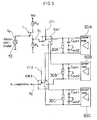
- FIG. 5 illustrates another example of the invention.
- the signal shaping circuit 20 can be used for different amplifiers.
- each of the three power amplifier 60A, 60B, 60C has connected a load 30A, 30B, 30C to its output terminals.
- a first capacitor C OUT1 and a second capacitor C OUT2 are connected between the first output terminal of the amplifier and the reference potential (e. g. ground potential GND) and a second output terminal of the amplifier and the reference potential, respectively.
- the capacitors C OUT1 and C OUT2 may be part of the amplifier output stage.
- the first output terminals of the amplifiers 60A, 60B, and 60C and the signal shaping circuit 20 are connected to the multiplex-switch SW1 such that either the first amplifier 60A, the second amplifier 60B, or the third amplifier 60C is connected to the signal shaping circuit 20.
- the second output terminals of the amplifiers 60A, 60B, and 60C and the signal shaping circuit 20 are connected to the multiplex-switch SW2 such that either the first amplifier 60A, the second amplifier 60B, or the third amplifier 60C is connected to the comparator.
- the multiplex-switches SW1 and SW2 have to switch synchronous, i.e. if the first output terminal of the second amplifier 60B is connected to the signal shaping circuit 20, then the second output terminal of second amplifier 60B has to be connected to the comparator.
- the multiplex-switches SW1 and SW2 may be controlled by control signals CT1 and CT2 which may be generated by the micro-controller 10.
- CT1 and CT2 may be generated by the micro-controller 10.
- a circuit as depicted in figure 2 is effectively achieved, wherein the connected amplifier can be switched. All variations and modifications of the circuit explained with respect to the example of FIG. 2 are also applicable to the examplary circuit of FIG. 5 .
- the number of connectable amplifiers is naturally not limited to three.
- the invention is not limited to detection of the load impedances of electro-acoustic transducers connected to the output stage of an amplifier, but may be employed to detect any load impedance connected to an arbitrary power supply.
- the capacitors C OUT1 and C OUT2 might be replaced by inductors.
Landscapes
- Engineering & Computer Science (AREA)
- Power Engineering (AREA)
- Multimedia (AREA)
- Amplifiers (AREA)
Abstract
Description
- The invention relates to a load testing circuit for detecting the presence of a defined load impedance connected to the output of a power amplifier.
- Many amplifier circuits require an overload protection for protecting their output-stages against destruction due to inappropriate loads attached thereto. Especially for audio amplifiers suitable loudspeakers (or other electro-acoustic transducers) are a prerequisite for a correct function of the amplifier.
- Modern amplifiers are often controlled by means of microcontrollers which take over many different tasks, such as selecting signal sources, processing user input, and so on. Micro-controllers also can be useful for fault-detection. Consequently there is a need for a circuit which allows for easily interfacing with a micro-controller and which allows for detecting inappropriate electro-acoustic transducers attached to an output-stage of a power amplifier in order to protect the output stage.
- A circuit for detecting a defined load of an electro-acoustic transducer is presented, the circuit comprising a signal generator providing a test signal of a defined bandwidth, an electro-acoustic transducer having a first and a second terminal, the first terminal being connected to the signal generator for receiving the test signal, an energy-storing element being connected to the second terminal of the electro-acoustic transducer, and providing an output signal, and measuring unit that measures the output signal or compares the output signal with a reference.
- Further, a method for testing an electro-acoustic transducer is presented, the method comprising the steps of: providing a test signal of a defined bandwidth, supplying the test signal to a first terminal of an electro-acoustic transducer, thereby providing an output signal at the second terminal of the electro-acoustic transducer, supplying the output signal to a measuring means for measuring the output signal or for comparing the output signal with a reference.
- The present invention can be better understood with reference to the following drawings and the description. The components in the figures are not necessarily to scale, emphasis instead being placed upon illustrating the principles of the invention. Moreover, in the figures, like reference numerals designate corresponding parts throughout the different views.
- FIG. 1
- is a simplified block diagram of a novel load testing circuit;
- FIG. 2
- is a more detailed circuit diagram of the example of
FIG. 1 ; - FIG. 3
- is a timing diagram illustrating a test signal before lowpass filtering;
- FIG. 4
- is a timing diagram illustrating different output signals corresponding to different impedance values of the load; and
- FIG. 5
- is a circuit diagram of another example of the load testing circuit.
- In the circuit of
Fig. 1 , a pulse signal Sp (cf.figure 3 ) is provided, for example, by a micro-controller. The pulse may be generated at an I/O-pin of an I/O-port of the micro-controller. Alternatively, a digital-to-analog converter output of the micro-controller may be used to provide the pulse signal Sp. The pulse signal comprises at least one pulse which is, for example, rectangular, and has a spectral bandwidth that may comprise at least parts of the spectral range audible by the human ear. - A test signal ST is derived from the (rectangular) pulse signal Sp by means of a
signal shaping circuit 20 providing the test signal ST which has a defined bandwidth determined by a transfer function of the signal shaping circuit shaping the signal Sp can be used. The bandwidth of the lowpass and/or the bandpass usually depends on the bandwidth of the electro-acoustic transducer that forms theload 30. As an example, the bandwidth of the bandpass may correspond to the bandwidth of the human ear which is about 20 kilohertz starting from approximately 20 Hertz. Alternatively, the signal shaping may already be performed by the above-mentioned analog-to-digital converter by converting an arbitrary synthesised signal of the desired bandwidth. - The
signal shaping circuit 20 may optionally comprise an amplifier to provide test signals ST having higher levels than the original pulse signal Sp or to perform an impedance conversion providing a low-output resistance of thesignal shaping circuit 20. Thesignal shaping circuit 20 is connected to a first terminal of theload 30, e.g. the electro-acoustic transducer, supplying the test signal ST to theload 30. A second terminal of theload 30 is connected to an energy storing element which may be, for example, a capacitor COUT2 inFIG. 2 . Capacitors are usually connected parallel to the output of an amplifier for reasons of EMC (electromagnetic compatibility) and ESD (electrostatic discharge) protection. These capacitors can be used as capacitors COUT1 and COUT2 ofFIG. 2 . - The energy storing element COUT2 provides an output signal So which is supplied to a comparator for further analysis. The energy storing element COUT2 is connected to the
load 30, such that the load's impedance and energy storing element COUT2 form a filter circuit disposed downstream of thesignal forming circuit 20. This filter circuit may represent a lowpass as shown inFIG. 2 or a bandpass but the use of other filter characteristics is applicable, too. In each case, the filter characteristics can be interpreted as a representation of the (generally complex) load impedance. In the case of a lowpass filter, the cut-off frequency, and respectively the time constant, of the lowpass depends on the load impedance. - The output signal So is supplied to a
comparator 40, e.g. a window-comparator 40 or a Schmitt-trigger for comparing the output signal to a threshold. The output signal So essentially represents the impulse response (of a band-limited pulse of the test signal ST) of a system formed byload 30 and energy storing element COUT2. Consequently, the load impedance is also represented by the slope of the output signal So such that the lower the load impedance, the steeper the slope of the output signal and the earlier a given threshold is reached by the output signal So. That is, the time period between initiation of the pulse signal SP (or the test signal ST) and the triggering ofcomparator 40 by the output signal So represents the load impedance. This time period can easily be measured by a micro-controller. Alternatively, the output-signal can directly supplied to an analog-to-digital converter port (A/D-port) of the micro-controller. In this case the functionality of the comparator 40 (or any other, even more complex analysis) can be implemented in software. - If the micro-controller detects an
inappropriate load impedance 30 it can initiate appropriate measures for protecting the power-amplifier output-stage to which the load-impedance is connected. Thus the above-described circuit can be used for overload protection of a output-stage of a power amplifier. For example, the micro-controller may deactivate the output-stage as long as it senses an unsuitable load impedance 30 (e.g. unsuitable loudspeakers) at the output of the power amplifier. -
FIG. 2 illustrates the circuit ofFIG. 1 in more detail. The pulse signal Sp can be generated by a micro-controller 10. - Therefore, for example, an output pin of the micro-controller can be connected to the
signal shaping circuit 20. In the example ofFIG. 2 the pulse signal Sp is received by the gate terminal of a junction field-effect transistor T. Of course any other type of transistor can be used for this purpose as well. The drain terminal of transistor T is connected to a first supply terminal receiving a first supply potential VDD via a resistor Rd. The source terminal of the transistor is connected to a second supply terminal receiving a second supply potential (e.g. ground potential GND) via resistor Rs. A first capacitor Cout1 is connected in parallel to the source resistor Rs. The test signal ST is provided by the source terminal of transistor T which is also connected to a first terminal of the load impedance (comprising a resistance Rload). The transistor circuit within thesignal shaping circuit 20 essentially forms a source-follower with source resistor Rs, a drain resistor Rd and the first capacitor Cout1. Drain and source resistors Rd and Rs form, together with the first capacitor Cout1, a first low pass, thus limiting the band width of the pulses in the pulse signal SP for providing a band limited test signal ST to the load impedance. This band limitation has to be performed, because some loads, especially electro-acoustic-transducers react in a bad manner or even can be destroyed if too high slopes (occurring e. g. in rectangular pulses) are applied. - The second terminal of the
load 30 is connected to the second supply terminal (ground potential) via an energy storing element which is a second capacitor Cout2 in the present case. As it can be easily seen fromFIG. 2 , load 30 and second capacitor Cout2 form a second low pass filter receiving the test signal ST and providing the output signal So. This output signal can be supplied to acomparator 40 or directly to an A/D-Port of a microcontroller as explained above reference toFIG. 1 . The output stage of apower amplifier 60 is connected to the first and the second terminal of theload 30. The circuit ofFIG. 2 can be used also for overload protection of the output stage. The micro-controller can therefore keep the output stage deactivated until the correct load impedance, i.e. an appropriate electro-acoustic transducer is detected. -
FIGs. 3 and 4 illustrate some exemplary experimental data.FIG. 3 is a timing diagram showing an exemplary pulse signal Sp having a pulse width of 5 ms.FIG. 4 shows output signals So for different load impedances (1mΩ, 4Ω, 16Ω, 1MΩ). Assuming the output signal So is supplied to a comparator, an appropriate threshold value may be, for example, 2 Volts. Assuming further, the threshold level is reached within about 4 µs, then it can be concluded the load impedance is about 4Ω. If the threshold level is reached in a shorter time, the impedance is too low, whereas, if the threshold value is reached later, the impedance is too high. -
FIG. 5 illustrates another example of the invention. By employing multiplex-switches SW1 and SW2 thesignal shaping circuit 20 can be used for different amplifiers. In the shown example each of the threepower amplifier load - The first output terminals of the
amplifiers signal shaping circuit 20 are connected to the multiplex-switch SW1 such that either thefirst amplifier 60A, thesecond amplifier 60B, or thethird amplifier 60C is connected to thesignal shaping circuit 20. The second output terminals of theamplifiers signal shaping circuit 20 are connected to the multiplex-switch SW2 such that either thefirst amplifier 60A, thesecond amplifier 60B, or thethird amplifier 60C is connected to the comparator. Of course the multiplex-switches SW1 and SW2 have to switch synchronous, i.e. if the first output terminal of thesecond amplifier 60B is connected to thesignal shaping circuit 20, then the second output terminal ofsecond amplifier 60B has to be connected to the comparator. - The multiplex-switches SW1 and SW2 may be controlled by control signals CT1 and CT2 which may be generated by the
micro-controller 10. In each switching state of the multiplex-switches SW1 and SW2 a circuit as depicted infigure 2 is effectively achieved, wherein the connected amplifier can be switched. All variations and modifications of the circuit explained with respect to the example ofFIG. 2 are also applicable to the examplary circuit ofFIG. 5 . The number of connectable amplifiers is naturally not limited to three. - It is to be understood, that the invention is not limited to detection of the load impedances of electro-acoustic transducers connected to the output stage of an amplifier, but may be employed to detect any load impedance connected to an arbitrary power supply. Dependent on the application the capacitors COUT1 and COUT2 might be replaced by inductors.
- Although various examples to realize the invention have been disclosed, it will be apparent to those skilled in the art that various changes and modifications can be made which will achieve some of the advantages of the invention without departing from the spirit and scope of the invention. It will be obvious to those reasonably skilled in the art that other components performing the same functions may be suitably substituted. Such modifications to the inventive concept are intended to be covered by the appended claims.
Claims (18)
- A circuit for detecting the load impedance of a load connected to an amplifier or to a power supply, the load impedance having a first and a second terminal, the circuit comprising:a signal generator providing a test signal of a defined bandwidth to the first terminal of the load impedance;an energy-storing element being connected to the second terminal of the load impedance and providing an output signal; anda measuring unit that measures the output signal or compares the output signal with a reference.
- A circuit for detecting a given load impedance of an electro-acoustic transducer which has a first and a second terminal being connected to an amplifier, the circuit comprising:a signal generator providing a test signal of a defined bandwidth to the first terminal of the electro-acoustic transducer;an capacitive element being connected to the second terminal of the electro-acoustic transducer and providing an output signal; anda measuring unit that measures the output signal or compares the output signal with a reference.
- The circuit of claim 1 or 2, where the signal generator comprises a micro-controller.
- The circuit of claim 3, where the signal generator further comprises a signal shaping circuit connected to an output pin of the micro-controller for providing the test signal.
- The circuit of claim 4, where the signal shaping circuit is a lowpass or a bandpass determining the bandwidth of the test signal.
- The circuit of claim 1 or 2, where the signal generator comprises a micro-controller with a digital-to-analog converter that provides a test signal of a defined bandwidth.
- The circuit of one of the claims 2 to 6, where the impedance of the electro-acoustic transducer and the capacitive element together form a lowpass receiving the test signal and providing the output signal.
- The circuit of one of the claims 1 to 7, where the measurement unit comprise a threshold detector for comparing the output signal with a reference signal and providing a digital output signal representing the result of the comparison.
- The circuit of claim 8, where the measurement unit comprises a micro-controller to which the digital output signal is supplied.
- The circuit of claim 8, where the threshold detector is a Schmitt-Trigger.
- The circuit of claim 8, where the threshold detector is a window-comparator.
- The circuit of claim 4, where the signal shaping circuit comprises:a semiconductor switch with a control terminal, a first and a second load terminal, the control terminal being connected to an output of the micro-controller;a first resistor connecting a first supply terminal and the first load terminal of the semiconductor switch;a second resistor connecting the second load terminal of the semiconductor switch and a second supply terminal; anda capacitor connected in parallel to the second resistor.
- The circuit of claim 1, where the energy-storing element is a inductive element.
- The circuit of one of the claims 1 to 13, which is switchable to different load impedances of different amplifiers by multiplex-switches.
- A method for testing an electro-acoustic transducer comprising the steps of:providing a test signal of a defined bandwidth; supplying the test signal to a first terminal of an electro-acoustic transducer, thereby providing an output signal at the second terminal of the electro-acoustic transducer; andmeasuring the output signal or comparing the output signal with a reference.
- The method of claim 15, where the step of providing a test signal comprises:providing a rectangular pulse signal, andsupplying the rectangular pulse signal to a lowpass or a highpass filter thereby providing the test signal.
- The method of claim 15, where the step of providing a test signal comprises synthesising a signal of a defined bandwidth by the use of an digital-to-analog converter.
- The method of one of the claims 15 to 17, further comprising:supplying the output signal to a threshold detector that compares the output signal to a threshold;providing a digital output signal representing the result of the comparison; andsupplying the digital output signal to a micro-controller.
Priority Applications (2)
| Application Number | Priority Date | Filing Date | Title |
|---|---|---|---|
| EP07010276A EP1995872A1 (en) | 2007-05-23 | 2007-05-23 | Load impedance testing circuit |
| US12/126,178 US8525536B2 (en) | 2007-05-23 | 2008-05-23 | Load testing circuit |
Applications Claiming Priority (1)
| Application Number | Priority Date | Filing Date | Title |
|---|---|---|---|
| EP07010276A EP1995872A1 (en) | 2007-05-23 | 2007-05-23 | Load impedance testing circuit |
Publications (1)
| Publication Number | Publication Date |
|---|---|
| EP1995872A1 true EP1995872A1 (en) | 2008-11-26 |
Family
ID=38669813
Family Applications (1)
| Application Number | Title | Priority Date | Filing Date |
|---|---|---|---|
| EP07010276A Withdrawn EP1995872A1 (en) | 2007-05-23 | 2007-05-23 | Load impedance testing circuit |
Country Status (2)
| Country | Link |
|---|---|
| US (1) | US8525536B2 (en) |
| EP (1) | EP1995872A1 (en) |
Cited By (4)
| Publication number | Priority date | Publication date | Assignee | Title |
|---|---|---|---|---|
| EP2114091A1 (en) | 2008-04-28 | 2009-11-04 | Harman Becker Automotive Systems GmbH | Load detection |
| CN103424625A (en) * | 2012-05-17 | 2013-12-04 | 雅马哈株式会社 | Test signal supplying device and semiconductor integrated circuit |
| WO2015038257A3 (en) * | 2013-09-16 | 2015-05-28 | Cirrus Logic, Inc. | Systems and methods for detection of load impedance of a transducer device coupled to an audio device |
| US9438982B2 (en) | 2013-09-16 | 2016-09-06 | Cirrus Logic, Inc. | Systems and methods for detection of load impedance of a transducer device coupled to an audio device |
Families Citing this family (4)
| Publication number | Priority date | Publication date | Assignee | Title |
|---|---|---|---|---|
| DK2744225T3 (en) * | 2012-12-17 | 2015-11-09 | Bernafon Ag | Hearing device and method for identifying an output transducer for a hearing aid |
| ITUB20155835A1 (en) | 2015-11-24 | 2017-05-24 | St Microelectronics Srl | CIRCUIT OF DIAGNOSIS TO DETECT THE STATE OF LOADING OF AN AUDIO AMPLIFIER, CORRESPONDING AUDIO SYSTEM, INTEGRATED CIRCUIT AND PROCEDURE |
| EP3252483B1 (en) * | 2016-06-02 | 2021-06-02 | Nxp B.V. | Load detector |
| EP3480950B1 (en) * | 2017-11-01 | 2022-09-07 | Nxp B.V. | Load detector and method of detecting a load |
Citations (9)
| Publication number | Priority date | Publication date | Assignee | Title |
|---|---|---|---|---|
| US4683591A (en) * | 1985-04-29 | 1987-07-28 | Emhart Industries, Inc. | Proportional power demand audio amplifier control |
| EP0446945A2 (en) * | 1990-03-16 | 1991-09-18 | Kabushiki Kaisha Toshiba | Electronic equipment incorporating an integrated BTL circuit |
| US5205619A (en) * | 1989-08-30 | 1993-04-27 | Wabco Westinghouse Fahrzeugbremsen Gmbh | Electronic circuit for surveillance of final amplifier and its load |
| US5216379A (en) * | 1992-06-26 | 1993-06-01 | Hamley James P | Dynamic bias amplifier |
| EP0661802A1 (en) * | 1993-12-31 | 1995-07-05 | STMicroelectronics S.r.l. | Operational amplifier protection circuit using, either in working conditions or at start-up, identical circuit elements for detecting permanent output abnormal conditions |
| DE19511242A1 (en) * | 1994-03-28 | 1995-10-05 | Matsushita Electric Works Ltd | Current supply e.g. for discharge lamp lighting control device |
| US5719526A (en) * | 1994-11-09 | 1998-02-17 | Crest Audio, Inc. | Internal load monitor for amplifier |
| EP1244208A1 (en) * | 2001-03-21 | 2002-09-25 | Pioneer Corporation | Power amplifying device |
| US20070057720A1 (en) * | 2005-08-25 | 2007-03-15 | D2Audio Corporation | Systems and methods for load detection and correction in a digital amplifier |
Family Cites Families (7)
| Publication number | Priority date | Publication date | Assignee | Title |
|---|---|---|---|---|
| US3067297A (en) * | 1960-02-26 | 1962-12-04 | Philco Corp | Apparatus for determining the polarities of stereophonic channel connections at anyselected point |
| JPS4937527A (en) * | 1972-08-09 | 1974-04-08 | ||
| US4550277A (en) * | 1984-09-24 | 1985-10-29 | Black & Decker Inc. | Overload detection and warning system for electric motors in power tools and the like |
| US6184919B1 (en) * | 1994-01-05 | 2001-02-06 | Robert R. Asprey | Extended length differentially driven analog video link |
| KR0165264B1 (en) * | 1993-03-08 | 1999-03-20 | Samsung Electronics Co Ltd | Television receiver having music room function |
| US6707919B2 (en) * | 2000-12-20 | 2004-03-16 | Multi Service Corporation | Driver control circuit |
| US20040086140A1 (en) * | 2002-11-06 | 2004-05-06 | Fedigan Stephen John | Apparatus and method for driving an audio speaker |
-
2007
- 2007-05-23 EP EP07010276A patent/EP1995872A1/en not_active Withdrawn
-
2008
- 2008-05-23 US US12/126,178 patent/US8525536B2/en not_active Expired - Fee Related
Patent Citations (9)
| Publication number | Priority date | Publication date | Assignee | Title |
|---|---|---|---|---|
| US4683591A (en) * | 1985-04-29 | 1987-07-28 | Emhart Industries, Inc. | Proportional power demand audio amplifier control |
| US5205619A (en) * | 1989-08-30 | 1993-04-27 | Wabco Westinghouse Fahrzeugbremsen Gmbh | Electronic circuit for surveillance of final amplifier and its load |
| EP0446945A2 (en) * | 1990-03-16 | 1991-09-18 | Kabushiki Kaisha Toshiba | Electronic equipment incorporating an integrated BTL circuit |
| US5216379A (en) * | 1992-06-26 | 1993-06-01 | Hamley James P | Dynamic bias amplifier |
| EP0661802A1 (en) * | 1993-12-31 | 1995-07-05 | STMicroelectronics S.r.l. | Operational amplifier protection circuit using, either in working conditions or at start-up, identical circuit elements for detecting permanent output abnormal conditions |
| DE19511242A1 (en) * | 1994-03-28 | 1995-10-05 | Matsushita Electric Works Ltd | Current supply e.g. for discharge lamp lighting control device |
| US5719526A (en) * | 1994-11-09 | 1998-02-17 | Crest Audio, Inc. | Internal load monitor for amplifier |
| EP1244208A1 (en) * | 2001-03-21 | 2002-09-25 | Pioneer Corporation | Power amplifying device |
| US20070057720A1 (en) * | 2005-08-25 | 2007-03-15 | D2Audio Corporation | Systems and methods for load detection and correction in a digital amplifier |
Cited By (9)
| Publication number | Priority date | Publication date | Assignee | Title |
|---|---|---|---|---|
| EP2114091A1 (en) | 2008-04-28 | 2009-11-04 | Harman Becker Automotive Systems GmbH | Load detection |
| CN103424625A (en) * | 2012-05-17 | 2013-12-04 | 雅马哈株式会社 | Test signal supplying device and semiconductor integrated circuit |
| CN103424625B (en) * | 2012-05-17 | 2016-01-06 | 雅马哈株式会社 | Test signal supply equipment and SIC (semiconductor integrated circuit) |
| US9535102B2 (en) | 2012-05-17 | 2017-01-03 | Yamaha Corporation | Test signal supplying device and semiconductor integrated circuit |
| WO2015038257A3 (en) * | 2013-09-16 | 2015-05-28 | Cirrus Logic, Inc. | Systems and methods for detection of load impedance of a transducer device coupled to an audio device |
| US9438982B2 (en) | 2013-09-16 | 2016-09-06 | Cirrus Logic, Inc. | Systems and methods for detection of load impedance of a transducer device coupled to an audio device |
| US9479869B2 (en) | 2013-09-16 | 2016-10-25 | Cirrus Logic, Inc. | Systems and methods for detection of load impedance of a transducer device coupled to an audio device |
| US9479868B2 (en) | 2013-09-16 | 2016-10-25 | Cirrus Logic, Inc. | Systems and methods for detection of load impedance of a transducer device coupled to an audio device |
| US9578417B2 (en) | 2013-09-16 | 2017-02-21 | Cirrus Logic, Inc. | Systems and methods for detection of load impedance of a transducer device coupled to an audio device |
Also Published As
| Publication number | Publication date |
|---|---|
| US8525536B2 (en) | 2013-09-03 |
| US20090051368A1 (en) | 2009-02-26 |
Similar Documents
| Publication | Publication Date | Title |
|---|---|---|
| US8525536B2 (en) | Load testing circuit | |
| US10171046B2 (en) | System and method for low distortion capacitive signal source amplifier | |
| US9083288B2 (en) | High level capable audio amplification circuit | |
| US9413317B2 (en) | System and method for high input capacitive signal amplifier | |
| CN1741685B (en) | Detection and control of diaphragm collapse in condenser microphones | |
| US10531211B2 (en) | Circuit and method for detecting the load status of an audio amplifier | |
| CN106658295B (en) | A kind of loudspeaker DC voltage detection circuit | |
| US10812920B2 (en) | Failure determination device and sound output device | |
| WO2009127568A1 (en) | Microphone assembly with integrated self-test circuitry | |
| US9042578B2 (en) | Microphone amplifier with overload circuit | |
| CN101499783A (en) | Gain automatic regulating circuit and electronic product using the same | |
| US8532313B2 (en) | Audio processing system for an audio output device | |
| EP2799891A1 (en) | Sensor circuit arrangement | |
| US8264275B2 (en) | Amplifier arrangement and method for signal amplification | |
| WO2022043652A1 (en) | Apparatus and methods for detecting a microphone condition | |
| US10891933B2 (en) | Audio processing system | |
| US10585539B2 (en) | High sensitivity readout circuit for touch panel | |
| US6060952A (en) | Amplifier circuit for infrared sensor | |
| TWI710214B (en) | Circuit having high-pass filter | |
| JP3700989B2 (en) | Signal processing device | |
| KR20000057450A (en) | Power supply for microphone | |
| US20170180856A1 (en) | Systems and methods of configuring a filter having at least two frequency response configurations | |
| JP2004311878A (en) | Static electricity suppression circuit | |
| CN120779208A (en) | Hall acquisition circuit testing device and system | |
| CN114421898A (en) | A power control circuit and system |
Legal Events
| Date | Code | Title | Description |
|---|---|---|---|
| PUAI | Public reference made under article 153(3) epc to a published international application that has entered the european phase |
Free format text: ORIGINAL CODE: 0009012 |
|
| AK | Designated contracting states |
Kind code of ref document: A1 Designated state(s): AT BE BG CH CY CZ DE DK EE ES FI FR GB GR HU IE IS IT LI LT LU LV MC MT NL PL PT RO SE SI SK TR |
|
| AX | Request for extension of the european patent |
Extension state: AL BA HR MK RS |
|
| 17P | Request for examination filed |
Effective date: 20090428 |
|
| 17Q | First examination report despatched |
Effective date: 20090602 |
|
| AKX | Designation fees paid |
Designated state(s): AT BE BG CH CY CZ DE DK EE ES FI FR GB GR HU IE IS IT LI LT LU LV MC MT NL PL PT RO SE SI SK TR |
|
| RAP1 | Party data changed (applicant data changed or rights of an application transferred) |
Owner name: HARMAN INTERNATIONAL INDUSTRIES, INC. |
|
| RAP1 | Party data changed (applicant data changed or rights of an application transferred) |
Owner name: APPLE INC. |
|
| STAA | Information on the status of an ep patent application or granted ep patent |
Free format text: STATUS: EXAMINATION IS IN PROGRESS |
|
| RAP1 | Party data changed (applicant data changed or rights of an application transferred) |
Owner name: APPLE INC. |
|
| STAA | Information on the status of an ep patent application or granted ep patent |
Free format text: STATUS: THE APPLICATION IS DEEMED TO BE WITHDRAWN |
|
| 18D | Application deemed to be withdrawn |
Effective date: 20180824 |