EP0446945A2 - Electronic equipment incorporating an integrated BTL circuit - Google Patents
Electronic equipment incorporating an integrated BTL circuit Download PDFInfo
- Publication number
- EP0446945A2 EP0446945A2 EP91104034A EP91104034A EP0446945A2 EP 0446945 A2 EP0446945 A2 EP 0446945A2 EP 91104034 A EP91104034 A EP 91104034A EP 91104034 A EP91104034 A EP 91104034A EP 0446945 A2 EP0446945 A2 EP 0446945A2
- Authority
- EP
- European Patent Office
- Prior art keywords
- circuit
- output
- current
- load
- electronic equipment
- Prior art date
- Legal status (The legal status is an assumption and is not a legal conclusion. Google has not performed a legal analysis and makes no representation as to the accuracy of the status listed.)
- Granted
Links
Images


Classifications
-
- H—ELECTRICITY
- H03—ELECTRONIC CIRCUITRY
- H03F—AMPLIFIERS
- H03F1/00—Details of amplifiers with only discharge tubes, only semiconductor devices or only unspecified devices as amplifying elements
- H03F1/52—Circuit arrangements for protecting such amplifiers
-
- H—ELECTRICITY
- H03—ELECTRONIC CIRCUITRY
- H03F—AMPLIFIERS
- H03F3/00—Amplifiers with only discharge tubes or only semiconductor devices as amplifying elements
- H03F3/30—Single-ended push-pull [SEPP] amplifiers; Phase-splitters therefor
- H03F3/3081—Duplicated single-ended push-pull arrangements, i.e. bridge circuits
Definitions
- This invention generally relates to on-vehicle electronic equipment, for example, and more particularly to electronic equipment containing an integrated BTL (Balanced Transformerless or Bridge-Tied Load) output circuit.
- BTL Bridge-Tied Load
- Low-frequency power amplifiers generally perform power-amplification of the input signal and supply the output signal to the speaker that in turn produces sound. Should the load (speaker, in this case) connected to the amplifier's output terminal be open-circuit for some reason, it could not receive the output signal so that it would produce no sound.
- Such sound-producing failure in electronic equipment incorporating low-frequency power amplifying circuitry such as a radio set, radio-cassette deck combination, stereo recording/reproducing apparatus, television set, and video tape recording/reproducing apparatus, may be ascribed to defective parts, wiring disconnections, poor plug connections and others.
- a defective device has been disassembled to check each circuit block of it for voltage, current, and resistance with measuring instruments such as a multimeter. This has involved a lot of labor and high technical skills.
- Fig. 1 shows an integrated BTL output circuit in car-carried electronic equipment and a load (a speaker, in this case) connected between output terminals TA and TB of the BTL output circuit that is composed of a first to fourth n-p-n transistors Q1 to Q4 at the output stage.
- the collector and emitter of the first transistor Q1 are connected to a power supply V CC and the output terminal TA, respectively; the collector and emitter of the second transistor Q2 are connected to the output terminal TA and the ground point V SS , respectively; the collector and emitter of the third transistor Q3 are connected to the power supply V CC and the output terminal TB, respectively; and the collector and emitter of the fourth transistor Q4 are connected to the output terminal TB and the ground point V SS , respectively.
- the bases of the transistors Q1 and Q4 are supplied with a driving signal S1 while the bases of the transistors Q2 and Q3 are supplied with a driving signal S2 opposite in phase to the signal S1, which enables on/off control.
- a preamplifier not shown
- transistors Q1 and Q4 are on, while transistors Q2 and Q3 are off.
- This allows the power supply V CC to flow current through the collector and emitter of the transistor Q1, the speaker SP that acts as a load, the collector and emitter of the transistor Q4, and to the ground point V SS .
- transistors Q2 and Q3 are on, while transistors Q1 and Q4 are off. This permits the power supply V CC to flow current through the collector and emitter of the transistor Q3, the load speaker SP, the collector and emitter of the transistor Q2 and to the ground point V SS .
- the BTL output circuit has the direct-current (DC) voltage at the TA and TB output-terminal pair set at nearly V CC /2 (in the case of V SS equal to 0 V) as shown in the equivalent circuit of Fig. 2, with the result that the DC voltage difference between output terminals TA and TB is theoretically zero.
- electronic equipment incorporating integrated BTL output circuitry has difficulty in building in a function that detects the load being in an open-circuit mode.
- an object of the present invention is to provide electronic equipment capable of detecting the load being in an open-circuit mode in an integrated BTL output circuit.
- the object of the present invention is achieved by electronic equipment comprising: a detecting circuit for detecting a load connected between two output terminals of a BTL output circuit being in an open-circuit mode, based on the magnitude of current flowing through the load; and a control circuit for controlling the BTL output circuit so as to put it in an operative state during normal operation, and in a nonoperative state upon detecting the load being in an open-circuit mode, and for controlling the detecting circuit so as to put it in a nonoperative state during normal operation, and in an operative state upon detecting the load being in an open-circuit mode.
- the detecting circuit checks the load for open-circuit with the BTL output circuit put in a nonoperative state by the control circuit.
- the detecting circuit determines whether or not the load, connected across the output-terminal pair of the BTL output circuit, is open-circuit based on the current flowing through the load. This makes it possible to detect the load being in an open-circuit mode, which is connected to electronic equipment incorporating a BTL output circuit.
- Fig. 3 shows: a BTL output circuit 20 built in a low-frequency power amplifier 10; a load (a speaker, in this case) SP; and a circuit for detecting the load SP being in an open-circuit mode, in electronic equipment according to an embodiment of the present invention.
- the amplifier 10 contains: the BTL output circuit 20; a bias circuit 11 for applying a bias voltage and a current to each circuit constituting the amplifier 10; a control circuit 12 for making switching control between the normal operation mode and the open-circuit load detecting mode; a detecting circuit 13 for detecting the load being in an open-circuit state; and an output circuit 14 for supplying to external circuitry a signal which tells that the load has been detected being in an open-circuit state.
- the load SP is connected across the TA-TB output terminal pair of the BTL output circuit 20.
- the on/off state of the switch SW1 between the output terminal TA and load SP equivalently represents a load SP-connected state (with switch SW1 on) and a load-disconnected state (with switch SW1 off), respectively.
- the control input terminal TC connected to the control circuit 12 is connected to a mode changeover signal output circuit 21 for supplying a mode switching signal, which is composed of a DC power supply E and a switch SW2.
- the circuit 21 applies the potential from the power supply E to the control circuit 12, thereby to detect that the load SP is in an open-circuit mode, and applies the ground potential to the circuit 12, thereby to operate the amplifier 10 in normal operation mode.
- the circuit 21 can be of the type which is controlled by a microcomputer, such that to applies the power-supply potential and the ground potential in response to a high-level output and a low-level output of the microcomputer, respectively.
- the output terminal TD connected to the output circuit 14 is connected to an indicating device 15 for telling the load SP is open-circuit.
- the BTL output circuit 20 is composed of a first to fourth n-p-n transistors Q1 to Q4 at the output stage.
- the collector and emitter of the first transistor Q1 are connected to a power supply V CC and the output terminal TA, respectively;
- the collector and emitter of the second transistor Q2 are connected to the output terminal TA and the ground point V SS , respectively;
- the collector and emitter of the third transistor Q3 are connected to the power supply V CC and the output terminal TB, respectively;
- the collector and emitter of the fourth transistor Q4 are connected to the output terminal TB and the ground point V SS , respectively.
- the bases of the transistors Q1 and Q4 are supplied with a driving signal S1, while the bases of the transistors Q2 and Q3 are supplied with a driving signal S2 opposite in phase to the signal S1, which enables on/off control.
- the driving signals S1 and S2 are produced by a preamplifier (not shown) or the like contained in the low-frequency power amplifier 10.
- the control circuit 12 is made up of n-p-n transistors Q5 and Q6, each base of which is connected to the control input terminal TC and each emitter of which is connected to the ground point V SS .
- the collector of the transistor Q5 is connected to the base of the p-n-p transistor Q7 in the detecting circuit 13 which is controlled through this connection.
- the collector of the transistor Q6 is connected to the control input terminal for controlling the bias circuit 11 which is controlled through this connection.
- the detecting circuit 13 is composed of the transistor Q7 and n-p-n transistor Q8 and resistors R3 to R5.
- the emitter, base, and collector of the transistor Q7 are connected to the power supply V CC , the collector of the transistor Q5, one end of each of the resistors R3 and R4.
- the other end of R3 is connected to the output terminal TA, while the other end of R4 is connected to the collector of the transistor Q8, the base and emitter of which are connected to the output terminal TB and the ground point V SS , respectively.
- the resistor R5 is connected between the base of the transistor Q8 and the ground point V SS .
- the output circuit 14 is composed of an n-p-n transistor Q9, the base, collector, and emitter of which are connected to the collector of the n-p-n transistor Q8, the output terminal TD, and the ground point V SS , respectively.
- the indicating device 15 essentially consists of a resistor R6, a microcomputer 16, and an indicator 17 for indicating that the load SP is open-circuit.
- One end of the resistor R6 is connected to an external power supply V DD , while the other end of it is connected to the output terminal TD.
- the microcomputer 16 detects the output level of the output terminal TD for display processing of the open-circuit state of the load SP.
- the indicator 17, whose display including on/off state representation is controlled by the microcomputer 16, is composed of, for example, light-emitting diodes or liquid-crystal display unit on the operator panel in electronic equipment.
- the control circuit 12 is operated so as to cause the bias circuit 11 to stop supplying a bias voltage and a current to each circuit to force the BTL output circuit 20 to stop operation with the result that there is no DC voltage appearing between the output terminals TA and TB, while it actuates the detecting circuit 13.
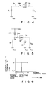
- This mechanism is illustrated in the equivalent circuit of Fig. 4.
- R1 is an internal resistance when the BTL output circuit 20 is viewed from one output terminal TA
- R2 is an internal resistance when the circuit 20 is viewed from the other output terminal TB.
- the detecting circuit 13 essentially consists of a constant-current source circuit 13a and a current detecting circuit 13b. As shown in Fig.
- the constant-current source circuit 13a supplies current to the output terminal TA, while the current detecting circuit 13b senses the current flowing through the other output terminal TB.
- the current flowing through the same terminal TB is theoretically zero, which makes it possible to detect the open-circuit load.
- the circuit shown in Fig. 3 has two operating modes each corresponding to the output levels of the mode changeover signal output circuit 21; it is in the normal operating mode with the output of the circuit 21 in a low level, whereas it is in the detecting mode for detecting open-circuit load with the circuit 21's output in a high level.
- the mode changeover signal output circuit 21 supplies a changeover signal to the control input terminal TC at a timing, for example, as shown in Fig.
- the bias circuit 11 is in an operative state and the detecting circuit 12 is in a nonoperative state with the mode changeover signal in a low level, whereas the bias circuit 11 is in a nonoperative state and the detecting circuit 13 is in an operative state with the signal in a high level. That is, with the mode changeover signal in a low level, each of the transistors Q6 and Q5 in the control circuit 12 is off, the bias circuit 11 is in normal operation, and the transistor Q7 of the detecting circuit 13 is off, which causes both the detecting circuit 13 and output circuit 14 to be nonoperative. Consequently, the low-frequency power amplifier 10 operates in normal mode, allowing the BTL output circuit 20 to actuate the load SP.
- each of the n-p-n transistors Q6 and Q5 in the control circuit 12 is on, the bias circuit 11 is nonoperative, and the transistor Q7 of the detecting circuit 13 is on, which stops supply of a bias voltage and a current to each circuit in the low-frequency power amplifier 10, causing the amplifier 10 to stop operation.
- the BTL output circuit 20 also stops operation, making the transistors Q1 to Q4 off.
- the control circuit 13 and output circuit 14 operate as follows, depending on whether or not the load SP is connected between the output terminals TA and TB (or whether switch SW1 is on or off).
- the power supply V CC flows current through the emitter to collector of the transistor Q7, resistor R3, output terminal TA, load SP, output terminal TB, resistor R5, and to the ground point V SS .
- the output terminal TD is charged via the resistor R6 by the power supply V DD in the indicating device 15 with the result that it is in a high level as shown in Fig. 7.
- the microcomputer 16 detects the high level at the output terminal TD, the indicator 17 is not driven, causing no display of open-circuit load SP.
- This invention is not restricted to the low-frequency power amplifier explained in the above embodiment, it may be applied to electronic equipment containing a motor driving circuit using an integrated BTL output circuit.
Abstract
Description
- This invention generally relates to on-vehicle electronic equipment, for example, and more particularly to electronic equipment containing an integrated BTL (Balanced Transformerless or Bridge-Tied Load) output circuit.
- Low-frequency power amplifiers generally perform power-amplification of the input signal and supply the output signal to the speaker that in turn produces sound. Should the load (speaker, in this case) connected to the amplifier's output terminal be open-circuit for some reason, it could not receive the output signal so that it would produce no sound.
- Such sound-producing failure in electronic equipment incorporating low-frequency power amplifying circuitry, such as a radio set, radio-cassette deck combination, stereo recording/reproducing apparatus, television set, and video tape recording/reproducing apparatus, may be ascribed to defective parts, wiring disconnections, poor plug connections and others. Conventionally, to investigate the causes, a defective device has been disassembled to check each circuit block of it for voltage, current, and resistance with measuring instruments such as a multimeter. This has involved a lot of labor and high technical skills.
- With this backdrop, it is desirable to provide highly reliable on-vehicle electronic equipment with an automatic function that checks the low-frequency power amplifier-actuated load for open-circuit. In the case of a low-frequency power amplifier containing an integrated BTL output circuit, however, it is very difficult to detect the load being in an open-circuit mode.
- The reason for this will be explained in detail, referring to Figs. 1 and 2. Fig. 1 shows an integrated BTL output circuit in car-carried electronic equipment and a load (a speaker, in this case) connected between output terminals TA and TB of the BTL output circuit that is composed of a first to fourth n-p-n transistors Q₁ to Q₄ at the output stage. The collector and emitter of the first transistor Q₁ are connected to a power supply VCC and the output terminal TA, respectively; the collector and emitter of the second transistor Q₂ are connected to the output terminal TA and the ground point VSS, respectively; the collector and emitter of the third transistor Q₃ are connected to the power supply VCC and the output terminal TB, respectively; and the collector and emitter of the fourth transistor Q₄ are connected to the output terminal TB and the ground point VSS, respectively. The bases of the transistors Q₁ and Q₄ are supplied with a driving signal S₁, while the bases of the transistors Q₂ and Q₃ are supplied with a driving signal S₂ opposite in phase to the signal S₁, which enables on/off control.
- In this arrangement, supplied to the transistors Q₁ to Q₄ are the driving signal S₁ and the driving signal S₂ opposite in phase to the signal S₁, each of which is produced by a preamplifier (not shown), including a phase inverting circuit, that receives a sine-wave signal, for example. During positive half-cycle of the sine-wave signal, transistors Q₁ and Q₄ are on, while transistors Q₂ and Q₃ are off. This allows the power supply VCC to flow current through the collector and emitter of the transistor Q₁, the speaker SP that acts as a load, the collector and emitter of the transistor Q₄, and to the ground point VSS. During the negative half-cycle, transistors Q₂ and Q₃ are on, while transistors Q₁ and Q₄ are off. This permits the power supply VCC to flow current through the collector and emitter of the transistor Q₃, the load speaker SP, the collector and emitter of the transistor Q₂ and to the ground point VSS.
- Regardless of the load being open-circuit or closed-circuit, the BTL output circuit has the direct-current (DC) voltage at the TA and TB output-terminal pair set at nearly VCC/2 (in the case of VSS equal to 0 V) as shown in the equivalent circuit of Fig. 2, with the result that the DC voltage difference between output terminals TA and TB is theoretically zero. During the operation of the BTL output circuit, the DC voltage at each of the output terminals TA and TB is thus approximately VCC/2 (VSS = 0 V), which makes it impossible to detect the open-circuit load.
- Application of integrated BTL output circuits is not restricted to the above-mentioned low-frequency power amplifiers, they may be applied to motor driving circuits, in which similar problems can be encountered.
- As described above, electronic equipment incorporating integrated BTL output circuitry has difficulty in building in a function that detects the load being in an open-circuit mode.
- Accordingly, an object of the present invention is to provide electronic equipment capable of detecting the load being in an open-circuit mode in an integrated BTL output circuit.
- The object of the present invention is achieved by electronic equipment comprising: a detecting circuit for detecting a load connected between two output terminals of a BTL output circuit being in an open-circuit mode, based on the magnitude of current flowing through the load; and a control circuit for controlling the BTL output circuit so as to put it in an operative state during normal operation, and in a nonoperative state upon detecting the load being in an open-circuit mode, and for controlling the detecting circuit so as to put it in a nonoperative state during normal operation, and in an operative state upon detecting the load being in an open-circuit mode.
- With this configuration, the detecting circuit checks the load for open-circuit with the BTL output circuit put in a nonoperative state by the control circuit. The detecting circuit determines whether or not the load, connected across the output-terminal pair of the BTL output circuit, is open-circuit based on the current flowing through the load. This makes it possible to detect the load being in an open-circuit mode, which is connected to electronic equipment incorporating a BTL output circuit.
- This invention can be more fully understood from the following detailed description when taken in conjunction with the accompanying drawings, in which:
- Fig. 1 is a circuit diagram for a conventional BTL output circuit with a load connected across a pair of output terminals of the circuit;
- Fig. 2 is an equivalent circuit diagram when the load is open-circuit and closed-circuit in the BTL output circuit of Fig. 1;
- Fig. 3 is a circuit diagram illustrating a BTL output circuit and a detecting circuit for detecting the load being in an open-circuit mode, both of which are incorporated in a low-frequency power amplifier contained in electronic equipment according to an embodiment of the present invention;
- Figs. 4 and 5 are equivalent circuits used to explain the principle of the circuits of Fig. 3 detecting the open-circuit load; and
- Figs. 6 and 7 are timing charts used to explain the way of detecting the load being in an open-circuit mode.
- Fig. 3 shows: a
BTL output circuit 20 built in a low-frequency power amplifier 10; a load (a speaker, in this case) SP; and a circuit for detecting the load SP being in an open-circuit mode, in electronic equipment according to an embodiment of the present invention. Theamplifier 10 contains: theBTL output circuit 20; a bias circuit 11 for applying a bias voltage and a current to each circuit constituting theamplifier 10; acontrol circuit 12 for making switching control between the normal operation mode and the open-circuit load detecting mode; a detectingcircuit 13 for detecting the load being in an open-circuit state; and anoutput circuit 14 for supplying to external circuitry a signal which tells that the load has been detected being in an open-circuit state. All these circuits are integrated into a single chip. The load SP is connected across the TA-TB output terminal pair of theBTL output circuit 20. The on/off state of the switch SW₁ between the output terminal TA and load SP equivalently represents a load SP-connected state (with switch SW₁ on) and a load-disconnected state (with switch SW₁ off), respectively. The control input terminal TC connected to thecontrol circuit 12 is connected to a mode changeoversignal output circuit 21 for supplying a mode switching signal, which is composed of a DC power supply E and a switch SW₂. Thecircuit 21 applies the potential from the power supply E to thecontrol circuit 12, thereby to detect that the load SP is in an open-circuit mode, and applies the ground potential to thecircuit 12, thereby to operate theamplifier 10 in normal operation mode. Thecircuit 21 can be of the type which is controlled by a microcomputer, such that to applies the power-supply potential and the ground potential in response to a high-level output and a low-level output of the microcomputer, respectively. The output terminal TD connected to theoutput circuit 14 is connected to an indicatingdevice 15 for telling the load SP is open-circuit. - The
BTL output circuit 20, like the equivalent in Fig. 1, is composed of a first to fourth n-p-n transistors Q₁ to Q₄ at the output stage. The collector and emitter of the first transistor Q₁ are connected to a power supply VCC and the output terminal TA, respectively; the collector and emitter of the second transistor Q₂ are connected to the output terminal TA and the ground point VSS, respectively; the collector and emitter of the third transistor Q₃ are connected to the power supply VCC and the output terminal TB, respectively; and the collector and emitter of the fourth transistor Q₄ are connected to the output terminal TB and the ground point VSS, respectively. The bases of the transistors Q₁ and Q₄ are supplied with a driving signal S₁, while the bases of the transistors Q₂ and Q₃ are supplied with a driving signal S₂ opposite in phase to the signal S₁, which enables on/off control. The driving signals S₁ and S₂ are produced by a preamplifier (not shown) or the like contained in the low-frequency power amplifier 10. - The
control circuit 12 is made up of n-p-n transistors Q₅ and Q₆, each base of which is connected to the control input terminal TC and each emitter of which is connected to the ground point VSS. The collector of the transistor Q₅ is connected to the base of the p-n-p transistor Q₇ in the detectingcircuit 13 which is controlled through this connection. The collector of the transistor Q₆ is connected to the control input terminal for controlling the bias circuit 11 which is controlled through this connection. - The detecting
circuit 13 is composed of the transistor Q₇ and n-p-n transistor Q₈ and resistors R₃ to R₅. The emitter, base, and collector of the transistor Q₇ are connected to the power supply VCC, the collector of the transistor Q₅, one end of each of the resistors R₃ and R₄. The other end of R₃ is connected to the output terminal TA, while the other end of R₄ is connected to the collector of the transistor Q₈, the base and emitter of which are connected to the output terminal TB and the ground point VSS, respectively. The resistor R₅ is connected between the base of the transistor Q₈ and the ground point VSS. - The
output circuit 14 is composed of an n-p-n transistor Q₉, the base, collector, and emitter of which are connected to the collector of the n-p-n transistor Q₈, the output terminal TD, and the ground point VSS, respectively. - The indicating
device 15 essentially consists of a resistor R₆, amicrocomputer 16, and anindicator 17 for indicating that the load SP is open-circuit. One end of the resistor R₆ is connected to an external power supply VDD, while the other end of it is connected to the output terminal TD. Themicrocomputer 16 detects the output level of the output terminal TD for display processing of the open-circuit state of the load SP. Theindicator 17, whose display including on/off state representation is controlled by themicrocomputer 16, is composed of, for example, light-emitting diodes or liquid-crystal display unit on the operator panel in electronic equipment. - The operation principle of detecting the load SP being in an open-circuit state (where the switch SW₁ is off) will be explained, referring to Figs. 4 and 5.
- To sense that the load is in an open-circuit mode, the
control circuit 12 is operated so as to cause the bias circuit 11 to stop supplying a bias voltage and a current to each circuit to force theBTL output circuit 20 to stop operation with the result that there is no DC voltage appearing between the output terminals TA and TB, while it actuates the detectingcircuit 13. This mechanism is illustrated in the equivalent circuit of Fig. 4. Here, R₁ is an internal resistance when theBTL output circuit 20 is viewed from one output terminal TA, whereas R₂ is an internal resistance when thecircuit 20 is viewed from the other output terminal TB. The detectingcircuit 13 essentially consists of a constant-current source circuit 13a and a current detectingcircuit 13b. As shown in Fig. 5, the constant-current source circuit 13a supplies current to the output terminal TA, while the current detectingcircuit 13b senses the current flowing through the other output terminal TB. In this case, with the load connected, current flows through the other output terminal TB, but with the load disconnected, the current flowing through the same terminal TB is theoretically zero, which makes it possible to detect the open-circuit load. - The operation of sensing that the load is in an open-circuit mode will be explained in detail. The circuit shown in Fig. 3 has two operating modes each corresponding to the output levels of the mode changeover
signal output circuit 21; it is in the normal operating mode with the output of thecircuit 21 in a low level, whereas it is in the detecting mode for detecting open-circuit load with thecircuit 21's output in a high level. When the mode changeoversignal output circuit 21 supplies a changeover signal to the control input terminal TC at a timing, for example, as shown in Fig. 6, the bias circuit 11 is in an operative state and the detectingcircuit 12 is in a nonoperative state with the mode changeover signal in a low level, whereas the bias circuit 11 is in a nonoperative state and the detectingcircuit 13 is in an operative state with the signal in a high level. That is, with the mode changeover signal in a low level, each of the transistors Q₆ and Q₅ in thecontrol circuit 12 is off, the bias circuit 11 is in normal operation, and the transistor Q₇ of the detectingcircuit 13 is off, which causes both the detectingcircuit 13 andoutput circuit 14 to be nonoperative. Consequently, the low-frequency power amplifier 10 operates in normal mode, allowing theBTL output circuit 20 to actuate the load SP. - With the mode changeover signal in a high level, each of the n-p-n transistors Q₆ and Q₅ in the
control circuit 12 is on, the bias circuit 11 is nonoperative, and the transistor Q₇ of the detectingcircuit 13 is on, which stops supply of a bias voltage and a current to each circuit in the low-frequency power amplifier 10, causing theamplifier 10 to stop operation. As a result, theBTL output circuit 20 also stops operation, making the transistors Q₁ to Q₄ off. With the transistor Q₇ on, thecontrol circuit 13 andoutput circuit 14 operate as follows, depending on whether or not the load SP is connected between the output terminals TA and TB (or whether switch SW₁ is on or off). - When the load SP is connected across the output terminals TA and TB (the same as the switch SW₁ being on), the power supply VCC flows current through the emitter to collector of the transistor Q₇, resistor R₃, output terminal TA, load SP, output terminal TB, resistor R₅, and to the ground point VSS. As a result of this, there is a voltage drop across the resistor R₅, which makes the transistor Q₈ on and the transistor Q₉ off. Consequently, the output terminal TD is charged via the resistor R₆ by the power supply VDD in the indicating
device 15 with the result that it is in a high level as shown in Fig. 7. When themicrocomputer 16 detects the high level at the output terminal TD, theindicator 17 is not driven, causing no display of open-circuit load SP. - On the other hand, with the load SP being open-circuit between the output terminals TA and TB (the same as the switch SW₁ being off), current does flow in the manner just mentioned above, but flows starting from the power supply VCC through the emitter and collector of the transistor Q₇, resistor R₄, and through the base of the transistor Q₉. As a result, the transistor Q₉ turns on, making the output terminal TD of a low level. When the
microcomputer 16 senses that the output terminal TD is in a low level as shown in Fig. 7, theindicator 17 is actuated to come on or blink. - With this arrangement, it is possible to determine whether or not a failure in the load SP is ascribed to its open-circuit. This makes it unnecessary to disassemble the device and check each circuit block of the device for volt age, current, resistance and other factors with instruments such as a multimeter, saving us a lot of labor. Additionally, for example, supply of detection initiating control signal from the
microcomputer 16 to the switch SW₂ at start-up makes it possible to provide an automatic checking function for load's open-circuit condition. Accordingly, the above-described low-frequency amplifier 10 is most suitable for cars requiring highly reliable circuitry. - This invention is not restricted to the low-frequency power amplifier explained in the above embodiment, it may be applied to electronic equipment containing a motor driving circuit using an integrated BTL output circuit.
- As described above, according to the present invention, it is possible to provide electronic equipment capable of automatically detecting the load being in an open-circuit mode in an integrated BTL output circuit.
- Reference signs in the claims are intended for better understanding and shall not limit the scope.
Claims (21)
- An electronic equipment incorporating an integrated BTL output circuit, characterized by comprising:
detecting means (13) for detecting a load (SP) connected between two output terminals (TA, TB) of said BTL output circuit (20) being in an open-circuit mode based on the magnitude of the current flowing across said two output terminal (TA, TB); and
control means (12) for controlling said BTL output circuit so as to put it in an operative state during normal operation and in a nonoperative state upon detecting said load (SP) being in an open-circuit mode and to put it in a nonoperative state during normal operation and in an operative state upon detecting said load (SP) being in an open-circuit mode. - The electronic equipment according to claim 1, characterized in that said detecting means (13) contains constant-current supplying means (Q₇, R₃) for supplying a constant current to one (TA) of said two output terminals (TA, TB), and current detecting means (R₅, Q₈) for detecting the current flowing through said load (SP) to the other (TB) of said two output terminals (TA, TB) by supplying a constant current from said constant-current supplying means (Q₇, R₃) to one (TA) of said two output terminals (TA, TB).
- The electronic equipment according to claim 2, characterized in that said constant-current supplying means contains a transistor (Q₇) one end of whose current path is connected to the power supply (VCC) and whose conduction is controlled by the output of said control means (12), and a resistor (R₃) one end of which is connected to the other end of the current path of said transistor (Q₇) and the other end of which is connected to one (TA) of said two output terminals (TA, TB).
- The electronic equipment according to claim 2, characterized in that said current detecting means contains a resistor (R₅) one end of which is connected to the other (TB) of said two output terminals (TA, TB) and the other end of which is connected to the ground point (VSS), and a transistor (Q₈) whose base is connected to the other (TB) of said two output terminals (TA, TB) and one end of whose current path is connected to the ground point (VSS) and the other end of whose current path is connected to said constant-current supplying means (Q₇, R₃) and which conducts the current from said constant-current supplying means (Q₇, R₃) to the ground point (VSS) upon detecting current flowing through said load (SP).
- The electronic equipment according to claim 1, characterized by further comprising output means (14) for outputting the result of said detecting means (13).
- The electronic equipment according to claim 5, characterized in that said output means (14) contains a transistor (Q₉) one end of whose current path is connected to the output terminal (TD) and the other end of whose current path is connected to the ground point (VSS) and whose conduction is controlled by the output signal from said detecting means (13).
- The electronic equipment according to claim 1, characterized in that said control means (12) contains a first transistor (Q₅) one end of whose current path is connected to said detecting means (13) and the other end of whose current path is connected to the ground point (VSS) and whose conduction is controlled by a mode changeover signal to control said detecting means (13), and a second transistor (Q₆) one end of whose current path is connected to bias means (11) and the other end of whose current path is connected to the ground point (VSS) and whose conduction is controlled by the mode changeover signal to control said bias means (11) for control of said BTL output circuit (20).
- The electronic equipment according to claim 1, characterized by further comprising mode changeover signal supplying means (21) for supplying a mode changeover signal to said control means (12).
- The electronic equipment according to claim 8, characterized in that said mode changeover signal supplying means (21) contains switching means (SW₂) for supplying to said control means (12) a low-level mode changeover signal during normal operation and a high-level mode changeover signal upon detecting said load (SP) being in an open-circuit mode.
- The electronic equipment according to claim 1, characterized by further comprising display means (15) for displaying the result of said detecting means (13).
- The electronic equipment according to claim 10, characterized in that said display means (15) contains a microcomputer (16) and an indicator (17).
- An electronic equipment incorporating an integrated BTL output circuit and driving a load connected between a first and second output terminals of said output circuit, characterized by comprising:
constant-current supplying means (Q₇, R₃) for supplying a constant current to said first output terminal (TA) of said BTL output circuit (20);
current detecting means (R₅, Q₈) for detecting current flowing through said load (SP) to said second output terminal (TB) by supplying a constant current from said constant-current supplying means (Q₇, R₃) to said first output terminal (TA);
output means (14) for outputting the result of said current detecting means (R₅, Q₈);
first control means (Q₆) for controlling said BTL output circuit (20) so as to put it in an operative state during normal operation and in a nonoperative state upon detecting said load (SP) being in an open-circuit mode; and
second control means (Q₅) for controlling said constant-current supplying means (Q₇, R₃) so as to put it in a nonoperative state during normal operation and in an operative state upon detecting said load (SP) being in an open-circuit mode. - The electronic equipment according to claim 12, characterized in that said constant-current supplying means contains a transistor (Q₇) one end of whose current path is connected to the power supply (VCC) and whose conduction is controlled by the output of said second control means (Q₅), and a resistor (R₃) one end of which is connected to the other end of the current path of said transistor (Q₇) and the other end of which is connected to said first output terminal (TA).
- The electronic equipment according to claim 12, characterized in that said current detecting means contains a resistor (R₅) one end of which is connected to said second output terminal (TB) and the other end of which is connected to the ground point (VSS), and a transistor (Q₈) whose base is connected to said second output terminal (TB) and one end of whose current path is connected to the ground point (VSS) and the other end of whose current path is connected to said constant-current supplying means (Q₇, R₃) and which conducts the current from said constant-current supplying means (Q₇, R₃) to the ground point (VSS) upon detecting current flowing through said load (SP).
- The electronic equipment according to claim 12, characterized in that said output means (14) contains a transistor (Q₉) one end of whose current path is connected to the output terminal (TD) and the other end of whose current path is connected to the ground point (VSS) and whose conduction is controlled on the basis of the output from said current detecting means (R₅, Q₈).
- The electronic equipment according to claim 12, characterized in that said first control means contains a transistor (Q₆) one end of whose current path is connected to bias means (11) for outputting a bias voltage and the other end of whose current path is connected to the ground point (VSS) and whose conduction is controlled by a mode changeover signal to control said bias means (11) for control of said BTL output circuit (20).
- The electronic equipment according to claim 12, characterized in that said second control means contains a transistor (Q₅) one end of whose current path is connected to said constant-current supplying means (Q₇) and the other end of whose current path is connected to the ground point (VSS) and whose conduction is controlled by a mode changeover signal to control said constant-current supplying means (Q₇, R₃).
- The electronic equipment according to claim 12, characterized by further comprising mode changeover signal supplying means (21) for supplying a mode changeover signal to said first and second control means (Q₅, Q₆).
- The electronic equipment according to claim 18, characterized in that said mode changeover signal supplying means (21), which contains a power supply (E) and a switch (SW₂) for switching between said power supply (E)'s potential and the ground point (VSS)'s potential, supplies to said first and second control means (Q₅, Q₆) the potential of the ground point (VSS) in normal operation mode and the potential of said power supply (E) upon detecting the load (SP) being in an open-circuit mode.
- The electronic equipment according to claim 12, characterized by further comprising display means (15) for displaying whether or not said load (SP) is in an open-circuit mode based on an output of said output means (14).
- The electronic equipment according to claim 20, characterized in that said display means contains a resistor (R₆) connected between an output node of said output means (14) and a power supply (VDD), a microcomputer (16) whose input node is connected to the output node of said output means (14), and an indicator (17) controlled by an output of said microcomputer (16).
Applications Claiming Priority (2)
| Application Number | Priority Date | Filing Date | Title |
|---|---|---|---|
| JP66693/90 | 1990-03-16 | ||
| JP2066693A JPH0748620B2 (en) | 1990-03-16 | 1990-03-16 | Electronic equipment |
Publications (3)
| Publication Number | Publication Date |
|---|---|
| EP0446945A2 true EP0446945A2 (en) | 1991-09-18 |
| EP0446945A3 EP0446945A3 (en) | 1992-04-08 |
| EP0446945B1 EP0446945B1 (en) | 1995-11-02 |
Family
ID=13323275
Family Applications (1)
| Application Number | Title | Priority Date | Filing Date |
|---|---|---|---|
| EP91104034A Expired - Lifetime EP0446945B1 (en) | 1990-03-16 | 1991-03-15 | Electronic equipment incorporating an integrated BTL circuit |
Country Status (5)
| Country | Link |
|---|---|
| US (1) | US5233496A (en) |
| EP (1) | EP0446945B1 (en) |
| JP (1) | JPH0748620B2 (en) |
| KR (1) | KR960004456B1 (en) |
| DE (1) | DE69114156T2 (en) |
Cited By (5)
| Publication number | Priority date | Publication date | Assignee | Title |
|---|---|---|---|---|
| US5719526A (en) * | 1994-11-09 | 1998-02-17 | Crest Audio, Inc. | Internal load monitor for amplifier |
| WO1998007232A1 (en) * | 1996-08-09 | 1998-02-19 | Philips Electronics N.V. | An amplifier and a method for detecting the presence of a load |
| EP1995872A1 (en) * | 2007-05-23 | 2008-11-26 | Harman Becker Automotive Systems GmbH | Load impedance testing circuit |
| CN109406989A (en) * | 2018-11-12 | 2019-03-01 | 深圳和而泰小家电智能科技有限公司 | A kind of load circuit detection method, load detecting circuit and electronic equipment |
| CN111033288A (en) * | 2017-09-15 | 2020-04-17 | 矢崎总业株式会社 | Abnormality detection device |
Families Citing this family (5)
| Publication number | Priority date | Publication date | Assignee | Title |
|---|---|---|---|---|
| US5835322A (en) * | 1997-07-07 | 1998-11-10 | Donald E. Smith | Ground fault interrupt circuit apparatus for 400-Hz aircraft electrical systems |
| US7034960B2 (en) * | 2001-08-16 | 2006-04-25 | Sun Chemical Corporation | System and method for managing electronic transmission of color data |
| JP2010190604A (en) * | 2009-02-16 | 2010-09-02 | Toyota Motor Corp | Apparatus for detecting open terminal, and semiconductor device |
| US8023236B2 (en) * | 2009-03-18 | 2011-09-20 | Hamilton Sundstrand Corporation | Precision ground fault detection for aircraft human body protection |
| USD826028S1 (en) * | 2017-05-30 | 2018-08-21 | Horizon Global Americas Inc. | Coupler lock |
Citations (5)
| Publication number | Priority date | Publication date | Assignee | Title |
|---|---|---|---|---|
| US3990020A (en) * | 1975-06-26 | 1976-11-02 | Hughes Aircraft Company | DC linear power amplifier |
| JPS5531301A (en) * | 1978-08-28 | 1980-03-05 | Toshiba Corp | Power distributor circuit |
| JPS6110780A (en) * | 1984-06-26 | 1986-01-18 | Omron Tateisi Electronics Co | Load disconnection detector |
| JPS6436109A (en) * | 1987-07-30 | 1989-02-07 | Nec Corp | Power amplifier circuit |
| EP0406967A1 (en) * | 1989-07-06 | 1991-01-09 | Koninklijke Philips Electronics N.V. | Amplifier arrangement |
Family Cites Families (6)
| Publication number | Priority date | Publication date | Assignee | Title |
|---|---|---|---|---|
| CA956576A (en) * | 1972-09-06 | 1974-10-22 | General Signal Corporation | Circuit integrity checking means for audio signal circuit |
| US3989908A (en) * | 1975-06-26 | 1976-11-02 | General Signal Corporation | Speaker supervision in a public address system |
| JPS58137329A (en) * | 1982-02-10 | 1983-08-15 | Nec Corp | Detecting circuit for breaking of input signal line |
| US4799019A (en) * | 1987-03-02 | 1989-01-17 | Charles Cooley | Electrical continuity load monitoring circuit |
| US4894605A (en) * | 1988-02-24 | 1990-01-16 | Digital Equipment Corporation | Method and on-chip apparatus for continuity testing |
| JP2542618Y2 (en) * | 1988-08-30 | 1997-07-30 | アルプス電気株式会社 | In-vehicle load condition detection drive |
-
1990
- 1990-03-16 JP JP2066693A patent/JPH0748620B2/en not_active Expired - Lifetime
-
1991
- 1991-03-13 US US07/668,626 patent/US5233496A/en not_active Expired - Lifetime
- 1991-03-15 DE DE69114156T patent/DE69114156T2/en not_active Expired - Fee Related
- 1991-03-15 EP EP91104034A patent/EP0446945B1/en not_active Expired - Lifetime
- 1991-03-16 KR KR1019910004194A patent/KR960004456B1/en not_active IP Right Cessation
Patent Citations (5)
| Publication number | Priority date | Publication date | Assignee | Title |
|---|---|---|---|---|
| US3990020A (en) * | 1975-06-26 | 1976-11-02 | Hughes Aircraft Company | DC linear power amplifier |
| JPS5531301A (en) * | 1978-08-28 | 1980-03-05 | Toshiba Corp | Power distributor circuit |
| JPS6110780A (en) * | 1984-06-26 | 1986-01-18 | Omron Tateisi Electronics Co | Load disconnection detector |
| JPS6436109A (en) * | 1987-07-30 | 1989-02-07 | Nec Corp | Power amplifier circuit |
| EP0406967A1 (en) * | 1989-07-06 | 1991-01-09 | Koninklijke Philips Electronics N.V. | Amplifier arrangement |
Non-Patent Citations (3)
| Title |
|---|
| PATENT ABSTRACTS OF JAPAN vol. 10, no. 157 (P-464)6 June 1986 & JP-A-61 010 780 ( TATEISHI DENKI KK ) 18 January 1986 * |
| PATENT ABSTRACTS OF JAPAN vol. 13, no. 230 (E-764)(3578) 26 May 1989 & JP-A-1 036 109 ( NEC CORP ) 7 February 1989 * |
| PATENT ABSTRACTS OF JAPAN vol. 4, no. 63 (E-10)(545) 13 May 1980 & JP-A-55 031 301 ( TOKYO SHIBAURA DENKI K.K. ) 5 March 1980 * |
Cited By (7)
| Publication number | Priority date | Publication date | Assignee | Title |
|---|---|---|---|---|
| US5719526A (en) * | 1994-11-09 | 1998-02-17 | Crest Audio, Inc. | Internal load monitor for amplifier |
| WO1998007232A1 (en) * | 1996-08-09 | 1998-02-19 | Philips Electronics N.V. | An amplifier and a method for detecting the presence of a load |
| US5905408A (en) * | 1996-08-09 | 1999-05-18 | U.S. Philips Corporation | Amplifier and a method for detecting the presence of a load |
| KR100457841B1 (en) * | 1996-08-09 | 2005-06-02 | 코닌클리케 필립스 일렉트로닉스 엔.브이. | How to detect the presence of amplifiers and loads |
| EP1995872A1 (en) * | 2007-05-23 | 2008-11-26 | Harman Becker Automotive Systems GmbH | Load impedance testing circuit |
| CN111033288A (en) * | 2017-09-15 | 2020-04-17 | 矢崎总业株式会社 | Abnormality detection device |
| CN109406989A (en) * | 2018-11-12 | 2019-03-01 | 深圳和而泰小家电智能科技有限公司 | A kind of load circuit detection method, load detecting circuit and electronic equipment |
Also Published As
| Publication number | Publication date |
|---|---|
| KR910017734A (en) | 1991-11-05 |
| EP0446945B1 (en) | 1995-11-02 |
| US5233496A (en) | 1993-08-03 |
| JPH03267770A (en) | 1991-11-28 |
| DE69114156D1 (en) | 1995-12-07 |
| EP0446945A3 (en) | 1992-04-08 |
| JPH0748620B2 (en) | 1995-05-24 |
| DE69114156T2 (en) | 1996-04-25 |
| KR960004456B1 (en) | 1996-04-06 |
Similar Documents
| Publication | Publication Date | Title |
|---|---|---|
| EP0446945B1 (en) | Electronic equipment incorporating an integrated BTL circuit | |
| US4752744A (en) | Balanced transformer-less amplifier circuit | |
| KR0168053B1 (en) | Load connection state detector circuit | |
| US4737696A (en) | Actuator drive circuit | |
| JPS62134576A (en) | Method of testing integrated module and circuit device | |
| JP3203521B2 (en) | Load disconnection detection circuit | |
| JP2000155619A (en) | Constant voltage power supply unit | |
| JP3202227B2 (en) | Circuit device having means for detecting disconnection of load circuit | |
| JPS6319097A (en) | Line abnormality monitor | |
| JP2675431B2 (en) | Load drive circuit | |
| JPH0635503A (en) | Industrial instrument output circuit | |
| JP3101688B2 (en) | Readout circuit having monitor terminal and magnetic recording apparatus using this circuit | |
| JPS61135390A (en) | Current measuring device of dc motor | |
| JP3146832B2 (en) | In-vehicle speaker device | |
| JP2530542Y2 (en) | DC detection circuit | |
| JPS599446Y2 (en) | Muting control signal generation circuit | |
| JPS59221800A (en) | Output circuit | |
| JPS59135682A (en) | Signal switching display device | |
| JP3439140B2 (en) | Drive circuit | |
| JPH0878962A (en) | Feeding system for operational amplifier circuit | |
| JPH0399508A (en) | Logarithmic conversion circuit | |
| JPS586610A (en) | Controller for transient characteristic of circuit during power feeding | |
| JPS62110652A (en) | Recording and reproducing device | |
| JPH0126277B2 (en) | ||
| JPH03233715A (en) | Power supply on/off circuit |
Legal Events
| Date | Code | Title | Description |
|---|---|---|---|
| PUAI | Public reference made under article 153(3) epc to a published international application that has entered the european phase |
Free format text: ORIGINAL CODE: 0009012 |
|
| 17P | Request for examination filed |
Effective date: 19910315 |
|
| AK | Designated contracting states |
Kind code of ref document: A2 Designated state(s): DE FR GB IT |
|
| PUAL | Search report despatched |
Free format text: ORIGINAL CODE: 0009013 |
|
| AK | Designated contracting states |
Kind code of ref document: A3 Designated state(s): DE FR GB IT |
|
| 17Q | First examination report despatched |
Effective date: 19940607 |
|
| GRAA | (expected) grant |
Free format text: ORIGINAL CODE: 0009210 |
|
| AK | Designated contracting states |
Kind code of ref document: B1 Designated state(s): DE FR GB IT |
|
| ITF | It: translation for a ep patent filed |
Owner name: JACOBACCI & PERANI S.P.A. |
|
| REF | Corresponds to: |
Ref document number: 69114156 Country of ref document: DE Date of ref document: 19951207 |
|
| ET | Fr: translation filed | ||
| PLBE | No opposition filed within time limit |
Free format text: ORIGINAL CODE: 0009261 |
|
| STAA | Information on the status of an ep patent application or granted ep patent |
Free format text: STATUS: NO OPPOSITION FILED WITHIN TIME LIMIT |
|
| 26N | No opposition filed | ||
| PGFP | Annual fee paid to national office [announced via postgrant information from national office to epo] |
Ref country code: DE Payment date: 19970321 Year of fee payment: 7 |
|
| PGFP | Annual fee paid to national office [announced via postgrant information from national office to epo] |
Ref country code: GB Payment date: 19980306 Year of fee payment: 8 |
|
| PGFP | Annual fee paid to national office [announced via postgrant information from national office to epo] |
Ref country code: FR Payment date: 19980310 Year of fee payment: 8 |
|
| PG25 | Lapsed in a contracting state [announced via postgrant information from national office to epo] |
Ref country code: DE Free format text: LAPSE BECAUSE OF NON-PAYMENT OF DUE FEES Effective date: 19981201 |
|
| PG25 | Lapsed in a contracting state [announced via postgrant information from national office to epo] |
Ref country code: GB Free format text: LAPSE BECAUSE OF NON-PAYMENT OF DUE FEES Effective date: 19990315 |
|
| GBPC | Gb: european patent ceased through non-payment of renewal fee |
Effective date: 19990315 |
|
| PG25 | Lapsed in a contracting state [announced via postgrant information from national office to epo] |
Ref country code: FR Free format text: LAPSE BECAUSE OF NON-PAYMENT OF DUE FEES Effective date: 19991130 |
|
| REG | Reference to a national code |
Ref country code: FR Ref legal event code: ST |
|
| PGFP | Annual fee paid to national office [announced via postgrant information from national office to epo] |
Ref country code: IT Payment date: 20070626 Year of fee payment: 17 |
|
| PG25 | Lapsed in a contracting state [announced via postgrant information from national office to epo] |
Ref country code: IT Free format text: LAPSE BECAUSE OF NON-PAYMENT OF DUE FEES Effective date: 20080315 |