EP1995799A2 - Organic insulator composition including a hydroxyl group-containing polymer, dielectric film and organic thin film transistor using the same - Google Patents
Organic insulator composition including a hydroxyl group-containing polymer, dielectric film and organic thin film transistor using the same Download PDFInfo
- Publication number
- EP1995799A2 EP1995799A2 EP08155916A EP08155916A EP1995799A2 EP 1995799 A2 EP1995799 A2 EP 1995799A2 EP 08155916 A EP08155916 A EP 08155916A EP 08155916 A EP08155916 A EP 08155916A EP 1995799 A2 EP1995799 A2 EP 1995799A2
- Authority
- EP
- European Patent Office
- Prior art keywords
- hydroxyl group
- group
- organic
- crosslinking agent
- insulator composition
- Prior art date
- Legal status (The legal status is an assumption and is not a legal conclusion. Google has not performed a legal analysis and makes no representation as to the accuracy of the status listed.)
- Withdrawn
Links
Images


Classifications
-
- H—ELECTRICITY
- H10—SEMICONDUCTOR DEVICES; ELECTRIC SOLID-STATE DEVICES NOT OTHERWISE PROVIDED FOR
- H10K—ORGANIC ELECTRIC SOLID-STATE DEVICES
- H10K10/00—Organic devices specially adapted for rectifying, amplifying, oscillating or switching; Organic capacitors or resistors having a potential-jump barrier or a surface barrier
- H10K10/40—Organic transistors
- H10K10/46—Field-effect transistors, e.g. organic thin-film transistors [OTFT]
- H10K10/462—Insulated gate field-effect transistors [IGFETs]
- H10K10/468—Insulated gate field-effect transistors [IGFETs] characterised by the gate dielectrics
- H10K10/471—Insulated gate field-effect transistors [IGFETs] characterised by the gate dielectrics the gate dielectric comprising only organic materials
-
- H—ELECTRICITY
- H01—ELECTRIC ELEMENTS
- H01B—CABLES; CONDUCTORS; INSULATORS; SELECTION OF MATERIALS FOR THEIR CONDUCTIVE, INSULATING OR DIELECTRIC PROPERTIES
- H01B3/00—Insulators or insulating bodies characterised by the insulating materials; Selection of materials for their insulating or dielectric properties
- H01B3/18—Insulators or insulating bodies characterised by the insulating materials; Selection of materials for their insulating or dielectric properties mainly consisting of organic substances
- H01B3/30—Insulators or insulating bodies characterised by the insulating materials; Selection of materials for their insulating or dielectric properties mainly consisting of organic substances plastics; resins; waxes
-
- H—ELECTRICITY
- H10—SEMICONDUCTOR DEVICES; ELECTRIC SOLID-STATE DEVICES NOT OTHERWISE PROVIDED FOR
- H10K—ORGANIC ELECTRIC SOLID-STATE DEVICES
- H10K10/00—Organic devices specially adapted for rectifying, amplifying, oscillating or switching; Organic capacitors or resistors having a potential-jump barrier or a surface barrier
- H10K10/40—Organic transistors
- H10K10/46—Field-effect transistors, e.g. organic thin-film transistors [OTFT]
- H10K10/462—Insulated gate field-effect transistors [IGFETs]
- H10K10/466—Lateral bottom-gate IGFETs comprising only a single gate
-
- H—ELECTRICITY
- H10—SEMICONDUCTOR DEVICES; ELECTRIC SOLID-STATE DEVICES NOT OTHERWISE PROVIDED FOR
- H10K—ORGANIC ELECTRIC SOLID-STATE DEVICES
- H10K85/00—Organic materials used in the body or electrodes of devices covered by this subclass
- H10K85/10—Organic polymers or oligomers
- H10K85/111—Organic polymers or oligomers comprising aromatic, heteroaromatic, or aryl chains, e.g. polyaniline, polyphenylene or polyphenylene vinylene
- H10K85/113—Heteroaromatic compounds comprising sulfur or selene, e.g. polythiophene
Definitions
- Example embodiments relate to an organic insulator composition including a hydroxyl group-containing polymer and a dielectric film and an organic thin film transistor (OTFT) using the same.
- Other example embodiments relate to an organic insulator composition, which includes a crosslinking agent and a hydroxyl group-containing oligomer or hydroxyl group-containing polymer, which may be used to form a thin film using a low-temperature wet process.
- a thin film transistor is used as a switching device for a flat panel display example (e.g., a liquid crystal display, an organic electroluminescent display, an electrophoretic display or the like).
- a semiconductor layer of the TFT is generally formed of an inorganic semiconductor material (e.g., silicon (Si)).
- an organic thin film transistor may be fabricated using a solution process at low temperatures, it may be easier to apply the OTFT to large-area flat panel displays, which are fabricated using only a deposition process.
- the OTFT may be prepared in the form of a fiber or a film due to the properties of the organic material. As such, an OTFT may be used in a flexible display device.
- the flexible display device may be formed on a thin and flexible substrate (e.g., paper).
- the flexible display device may have increased flexibility (including bendability and windability) and/or a higher resistance to damage and impact.
- an organic insulator may be formed into a thin film on a plastic substrate and cured by performing a curing process (e.g., thermal curing).
- a curing process e.g., thermal curing
- Thermal curing may be performed at a substantially high temperature of 150°C and above. Because of the substantially high temperature, thermal deformation of the plastic substrate may occur during the insulator curing process, leading to misalignment. As such, electrical properties of the device may deteriorate.
- organic gate insulating films which may be subjected to a low-temperature process to decrease negative influences on the substrate or other process films, is being conducted.
- organic insulating film e.g., polyimide, polyvinylalcohol, poly(vinylphenol-maleimide), or photoacryl
- it may not increase the properties of the device to the extent that it can be considered a comparable alternative to conventional inorganic insulating films.
- Example embodiments relate to an organic insulator composition including a hydroxyl group-containing polymer and a dielectric film and an organic thin film transistor (OTFT) using the same.
- Other example embodiments relate to an organic insulator composition, which includes a crosslinking agent and a hydroxyl group-containing oligomer or hydroxyl group-containing polymer, which may be used to form a thin film using a low-temperature wet process.
- Example embodiments also provide an organic insulator composition, which may be formed into a thin film using a wet process at temperatures lower than 130°C.
- Other example embodiments provide an organic insulator composition that may impart desired electrical properties upon the fabrication of an OTFT.
- Example embodiments also provide a dielectric film, which may be prepared using a low-temperature wet process, and an OTFT, which includes the dielectric film, providing higher charge mobility and/or lower threshold voltage.
- the organic insulator composition may include a hydroxyl group-containing oligomer or hydroxyl group-containing polymer.
- the organic insulator composition may also include a crosslinking agent.
- the hydroxyl group-containing oligomer or hydroxyl group-containing polymer may be selected from the group consisting of polyvinylalcohol, polyvinylphenol, poly(hydroxyphenylmaleimide-co-hydroxystyrene), polyhydroxyimide, poly(vinylalcohol-co-ethylene) and copolymers thereof.
- the hydroxyl group-containing oligomer or hydroxyl group-containing polymer may be selected from the group consisting of oligomer or polymers represented by Formulas (1) to (3) below: wherein X and Yare each independently a tetravalent aromatic or aliphatic organic group, Z is hydrogen or a crosslinkable monovalent organic group, and n is an integer from 10 to 1,000; wherein Z and Z' are each independently hydrogen, a hydroxyl group, or a phenol group, and n is an integer from 10 to 1,000; and wherein l , m , and n are each independently an integer from 0 to 1,000, in which / and m are not both 0.
- Formulas (1) to (3) wherein X and Yare each independently a tetravalent aromatic or aliphatic organic group, Z is hydrogen or a crosslinkable monovalent organic group, and n is an integer from 10 to 1,000; wherein Z and Z' are each independently hydrogen, a hydroxyl group, or a phenol group, and n is an
- a dielectric film which includes a compound in which hydroxyl group-containing oligomers or hydroxyl group-containing polymers are connected via crosslinking using a crosslinking agent having two or more vinyl ether groups.
- the dielectric film may include the compound represented by Formula (11) below: wherein X and Y are each independently a tetravalent aromatic or aliphatic organic group, and B is a divalent aromatic or aliphatic organic group.
- Example embodiments provide an OTFT including a gate electrode formed on a substrate; a gate insulating layer formed on the gate electrode; source and drain electrodes formed on the gate insulating layer; and an organic semiconductor layer contacting the gate insulating layer, wherein the gate insulating layer may be the dielectric film according to example embodiments.
- FIGS. 1-2 represent nonlimiting, example embodiments as described herein.
- FIG. 1A is a diagram illustrating a schematic cross-sectional view of the bottom contact type OTFT according to example embodiments
- FIG. 1B is diagram illustrating a schematic cross-sectional view of the top contact type OTFT according to example embodiments
- FIG. 2 is a graph illustrating current transfer properties of OTFTs fabricated in according to Examples 1 and 2 and Comparative Example 1 (discussed below).
- first, second, third etc. may be used herein to describe various elements, components, regions, layers and/or sections, these elements, components, regions, layers and/or sections should not be limited by these terms. These terms are only used to distinguish one element, component, region, layer or section from another region, layer or section. Thus, a first element, component, region, layer or section discussed below could be termed a second element, component, region, layer or section without departing from the scope of example embodiments.
- spatially relative terms such as “beneath,” “below,” “lower,” “above,” “upper” and the like, may be used herein for ease of description to describe one element or a relationship between a feature and another element or feature as illustrated in the figures. It will be understood that the spatially relative terms are intended to encompass different orientations of the device in use or operation in addition to the orientation depicted in the Figures. For example, if the device in the figures is turned over, elements described as “below” or “beneath” other elements or features would then be oriented “above” the other elements or features. Thus, for example, the term “below” can encompass both an orientation which is above as well as below. The device may be otherwise oriented (rotated 90 degrees or viewed or referenced at other orientations) and the spatially relative descriptors used herein should be interpreted accordingly.
- Example embodiments are described herein with reference to cross-sectional illustrations that are schematic illustrations of idealized embodiments (and intermediate structures). As such, variations from the shapes of the illustrations as a result, for example, of manufacturing techniques and/or tolerances, may be expected. Thus, example embodiments should not be construed as limited to the particular shapes of regions illustrated herein but may include deviations in shapes that result, for example, from manufacturing. For example, an implanted region illustrated as a rectangle may have rounded or curved features and/or a gradient (e.g., of implant concentration) at its edges rather than an abrupt change from an implanted region to a non-implanted region.
- a gradient e.g., of implant concentration
- a buried region formed by implantation may result in some implantation in the region between the buried region and the surface through which the implantation may take place.
- the regions illustrated in the figures are schematic in nature and their shapes do not necessarily illustrate the actual shape of a region of a device and do not limit the scope.
- Example embodiments relate to an organic insulator composition including a hydroxyl group-containing polymer and a dielectric film and an organic thin film transistor (OTFT) using the same.
- Other example embodiments relate to an organic insulator composition, which includes a crosslinking agent and a hydroxyl group-containing oligomer or hydroxyl group-containing polymer, which may be used to form a thin film using a low-temperature wet process.
- hydroxyl group-containing oligomer or hydroxyl group-containing polymer means an oligomer or polymer that contains a hydroxyl group in the main chain or side chain of the oligomer or polymer.
- examples of the hydroxyl group-containing oligomer or hydroxyl group-containing polymer include an oligomer or polymer containing a vinyl alcohol or a vinyl phenyl moiety in the main chain or side chain thereof.
- the organic insulator composition is characterized in that a hydroxyl group-containing oligomer or hydroxyl group-containing polymer, functioning as a base resin, is mixed with a crosslinking agent having two or more vinyl ether groups.
- the mixture may be formed into a thin film using a wet process (e.g., spin coating, roll coating, or printing) at temperatures lower than 130°C.
- the hydroxyl group-containing oligomer or hydroxyl group-containing polymer of the organic insulator composition may be selected from the group consisting of polyvinylalcohol, polyvinylphenol, poly(hydroxyphenyl maleimide-co-hydroxystyrene), polyhydroxyimide, poly(vinyl alcohol-co-ethylene) and copolymers thereof.
- the hydroxyl group-containing oligomer or hydroxyl group-containing polymer may be selected from the group consisting of oligomers or polymers represented by Formula (1) to (3) below: wherein X and Y are each independently a tetravalent aromatic or aliphatic organic group, Z is hydrogen or a crosslinkable monovalent organic group, and n is an integer from 10 to 1,000; wherein Z and Z' are each independently hydrogen, a hydroxyl group, or a phenol group, and n is an integer from 10 to 1,000; and wherein l , m , and n are each independently an integer from 0 to 1,000, in which / and m are not both 0.
- Formula (1) to (3) wherein X and Y are each independently a tetravalent aromatic or aliphatic organic group, Z is hydrogen or a crosslinkable monovalent organic group, and n is an integer from 10 to 1,000; wherein Z and Z' are each independently hydrogen, a hydroxyl group, or a phenol group, and n is an
- X may be selected from the group consisting of and In Formula (1), Y may be selected from the group consisting of In Formula (1), Z may be selected from the group consisting of hydrogen (H), and -O-C ⁇ N.
- hydroxyl group-containing oligomer or hydroxyl group-containing polymer include, but are not limited to, oligomers or polymers represented by Formulas (4) to (10) below: wherein, in Formulas (4) to (9), n is an integer from 10 to 1,000; and wherein x and y are each independently an integer from 10 to 1,000.
- the crosslinking agent may be a compound having two or more vinyl ether groups.
- Crosslinking agents well-known in the art may be used so long as the crosslinking agent achieves the purpose of set forth by example embodiments.
- crosslinking agent examples include, but are not limited to, 2,2'-bis(4-(2-(vinyloxy)ethoxy)phenyl)propane (BPA-DEVE), 1,1,1-tris(4-(2-(vinyloxy)ethoxy]phenyl)ethane, 1,3,5-tris(2-(vinyloxy)ethoxy)benzene, poly(ethylene glycol)divinyl ether, 4,4'-bis-but-3-enyloxy-biphenyl, and 1,5-bis-but-3-enyloxy-naphthalene.
- BPA-DEVE 2,2'-bis(4-(2-(vinyloxy)ethoxy)phenyl)propane
- 1,1,1-tris(4-(2-(vinyloxy)ethoxy]phenyl)ethane 1,3,5-tris(2-(vinyloxy)ethoxy)benzene
- poly(ethylene glycol)divinyl ether 4,4'-bis
- an amount of the hydroxyl group-containing oligomer or hydroxyl group-containing polymer varies depending on the application in which the oligomer or polymer is used.
- the hydroxyl group-containing oligomer or hydroxyl group-containing polymer may be used in an amount ranging from about 5 wt% to about 60 wt%. If the amount of the hydroxyl group-containing oligomer or hydroxyl group-containing polymer exceeds 60 wt%, the viscosity of the composition may be too high, making it difficult to completely dissolve the hydroxyl group-containing oligomer or hydroxyl group-containing polymer and/or to remove impurities by filtration.
- the amount of the hydroxyl group-containing oligomer or hydroxyl group-containing polymer is less than 5 wt%, it may be difficult to subsequently form a film through deposition processes (e.g., spin coating) due to the substantially low concentration of the oligomer or polymer. If the amount of the hydroxyl group-containing oligomer or hydroxyl group-containing polymer is less than 5 wt%, flatness may decrease.
- an amount of the crosslinking agent varies depending on the amount of the hydroxyl group-containing oligomer or hydroxyl group-containing polymer.
- the amount of the crosslinking agent may be in a range between the lower limit of Equation 1 (below) and the upper limit of Equation 2 (below), based on the weight of the hydroxyl group-containing oligomer or hydroxyl group-containing polymer (or the base resin).
- the amount of the crosslinking agent exceeds the upper limit, the electrical properties of the device fabricated using the composition may deteriorate due to the presence of any unreacted crosslinking agent. If the amount is less than the lower limit, the degree of curing of the hydroxyl group-containing oligomer or hydroxyl group-containing polymer may decrease, causing a variety of problems.
- M . W . of crosslinking agent M . W . of repeating unit of base resin ⁇ number of OH groups in repeating unit of base resin number of vinylether groups in crosslinking agent ⁇ 100 ⁇ 0.1 parts
- M . W . of crosslinking agent M . W . of repeating unit of base resin ⁇ number of OH groups in repeating unit of base resin number of vinylether groups in crosslinking agent ⁇ 120 parts
- the organic insulator composition according to example embodiments may be applied (or formed) on a substrate, dried, and cured to obtain a dielectric film.
- the dielectric film may be used as an organic insulating layer of an OTFT.
- use of the dielectric film is not particularly limited.
- the hydroxyl group of the hydroxyl group-containing oligomer or hydroxyl group-containing polymer, functioning as the base resin may be subjected to acetalation with the vinyl ether groups of the crosslinking agent such that the hydroxyl group-containing oligomers or hydroxyl group-containing polymers may be linked (or connected) to each other by the crosslinking agent.
- the organic insulator composition may be cured at temperatures lower than 130°C.
- Reaction 1 (below) illustrates the acetalation mechanism between the hydroxyl group of polyhydroxyimide (1) of Formula (4) and the vinyl ether group of the crosslinking agent, 2,2'-bis(4-(2-(vinyloxy)ethoxy)phenyl)propane (2).
- the organic insulator composition (3) may be applied to flexible display devices.
- the dielectric film according to example embodiments is characterized by the inclusion of a compound in which hydroxyl group-containing oligomers or hydroxyl group-containing polymers are connected via crosslinking using a crosslinking agent having two or more vinyl ether groups.
- a compound in which the hydroxyl group-containing oligomers or hydroxyl group-containing polymers are connected to each other by the crosslinking agent include a compound of Formula (11) below: wherein X and Y are each independently a tetravalent aromatic or aliphatic organic group, and B is a divalent aromatic or aliphatic organic group.
- X is selected from the group consisting of
- Y is selected from the group consisting of
- Example embodiments also provide an OTFT including the dielectric film as described above.
- the OTFT may include a substrate, a gate electrode, a gate insulating layer, source/drain electrodes, and an organic semiconductor layer.
- the layer structure of the OTFT is not limited thereto.
- FIG. 1A is a diagram illustrating a schematic cross-sectional view of a bottom contact type OTFT according to example embodiments.
- the OTFT may have a bottom contact (BC) structure including a substrate 10, a gate electrode 20, a gate insulating layer 30, a source electrode 40, a drain electrode 50 and/or an organic semiconductor layer 60.
- the substrate 10, a gate electrode 20, a gate insulating layer 30, a source electrode 40, a drain electrode 50 and an organic semiconductor layer 60 may be sequentially laminated such that the organic semiconductor layer 60 is formed on the source electrode 40 and the drain electrode 50.
- FIG. 1B is diagram illustrating a schematic cross-sectional view of a top contact type OTFT according to example embodiments.
- the OTFT may be formed (or realized) in a top contact (TC) structure, in which a metal electrode (not shown) is subsequently formed on the organic semiconductor layer 60 through a deposition process (e.g., mask deposition).
- TC top contact
- the OTFT is not limited to these structures.
- the OTFT may have a top gate structure or a bottom gate structure.
- the gate insulating layer may be formed using the organic insulator composition including the hydroxyl group-containing oligomer or hydroxyl group-containing polymer and the crosslinking agent in order to increase the electrical properties of the device and/or to facilitate the process for forming the thin film of the insulating layer.
- the insulating layer of the OTFT may be prepared using the organic insulator composition disclosed herein.
- the insulating layer of the OTFT may include an organic insulator containing polyimide, benzocyclobutene, parylene, polyacrylate, polyvinylbutyral and/or polyvinyl phenol.
- the insulating layer of the OTFT may be formed into a thin film through screen printing, printing, dipping, ink jetting or laser deposition, spin coating or other like methods.
- the insulating layer of the OTFT may be provided in the form of a thin film using a wet process (e.g., printing coating, spin coating, bar coating, etc.) under normal pressure opposed to a conventional plasma-enhanced chemical vapor deposition process for forming a silicon (Si) thin film.
- a wet process e.g., printing coating, spin coating, bar coating, etc.
- the insulating layer of the OTFT may be subjected to a rollto-roll process using a plastic substrate to realize (or form) a lower costing TFT.
- the OTFT according to example embodiments may be applied to (or used in) driving elements for driving plastic-based active organic electroluminescent devices, smart cards or plastic chips for inventory tags.
- the organic semiconductor layer may be formed of materials well-known in the art. Examples of materials used to form the organic semiconductor layer may include, but are not limited to, pentacene, copper phthalocyanine, polythiophene, polyaniline, polyacetylene, polypyrrole, polyphenylenevinylene and derivatives thereof.
- Examples of materials used for the substrate include, but are not limited to, glass, polyethylene naphthalate (PEN), polyethylene terephthalate (PET), polycarbonate, polyvinylbutyral, polyacrylate, polyimide, polynorbornene, polyethersulfone (PES) or the like.
- the gate electrode and the source/drain electrodes may be formed of metals well-known in the art. Examples of metals that may be used for the gate electrode and the source/drain electrodes include, but are not limited to, gold (Au), silver (Ag), aluminum (Al), nickel (Ni), indium tin oxide (ITO), molybdenum (Mo), tungsten (W) or similar metals.
- the resulting polyhydroxyimide solution was mixed with 0.288 g of 2,2'-bis(4-(2-(vinyloxy)ethoxy)phenyl)propane (crosslinking agent).
- the resulting mixture was filtered using a 0.45 ⁇ m filter to obtain an organic insulator composition.
- molybdenum for a gate electrode was deposited with a thickness of 1000 ⁇ by sputtering.
- the insulator composition (described above) was applied thereon through spin coating at 1500 rpm for 50 sec and thermally treated at 130°C for 5 min to form a film having a thickness of 600nm.
- a 1 wt% polythiophene solution in chlorobenzene was applied on the 600nm film by spin coating at 1000 rpm for 30 sec and thermally treated at 100°C for 10 min to form a film having a thickness of 500 ⁇ .
- Gold (Au) for source/drain electrodes was deposited to a thickness of 70 nm on the 500 ⁇ film by sputtering, fabricating an OTFT.
- the resulting polyhydroxyimide solution was mixed with 0.575 g of 2,2'-bis(4-(2-(vinyloxy)ethoxy)phenyl)propane (crosslinking agent).
- the mixture was filtered using a 0.45 ⁇ m filter to obtain an organic insulator composition.
- the organic insulator composition was used to obtain an OTFT in the same manner as in Example 1.
- FIG. 2 is a graph illustrating current transfer properties of OTFTs fabricated in according to Examples 1 and 2 and Comparative Example 1. Referring to FIG. 2 , the current transfer properties of the OTFTs were measured using a semiconductor characterization system (4200-SCS) available from Keithley. The measured values are shown in Table 1 below.
- the on/off current ratio (I on /I off ) was taken from the ratio of maximum current in the on-state to minimum current in the off-state.
- the degree of curing of the gate insulating layer increases, then the mobility increases six fold, the on/off current ratio increases and the threshold voltage is approximately 0 V..
- example embodiments provide an organic insulator composition including a hydroxyl group-containing polymer and a dielectric film and an OTFT using the same.
- the organic insulator composition may be cured at temperatures lower than 130°C.
- the organic insulator composition according to example embodiments has is more chemically resistance.
- the organic insulator composition may be used to form a thin film in a low-temperature wet process.
- the organic insulator composition may be used in the fabrication of a flexible display device.
- the composition according to example embodiments may impart increased electrical properties if used in the fabrication of an OTFT. If a curing process is performed, the organic insulator composition may prevent (or reduce) the formation of reaction by-products, increasing the electrical properties.
Landscapes
- Physics & Mathematics (AREA)
- Spectroscopy & Molecular Physics (AREA)
- Thin Film Transistor (AREA)
- Formation Of Insulating Films (AREA)
Abstract
Description
- Example embodiments relate to an organic insulator composition including a hydroxyl group-containing polymer and a dielectric film and an organic thin film transistor (OTFT) using the same. Other example embodiments relate to an organic insulator composition, which includes a crosslinking agent and a hydroxyl group-containing oligomer or hydroxyl group-containing polymer, which may be used to form a thin film using a low-temperature wet process.
- In general, a thin film transistor (TFT) is used as a switching device for a flat panel display example (e.g., a liquid crystal display, an organic electroluminescent display, an electrophoretic display or the like). A semiconductor layer of the TFT is generally formed of an inorganic semiconductor material (e.g., silicon (Si)).
- According to the recent trend toward the fabrication of large, inexpensive and flexible displays, research is being conducted on organic semiconductor materials that may replace expensive inorganic materials that require a high-temperature vacuum process. Because an organic thin film transistor (OTFT) may be fabricated using a solution process at low temperatures, it may be easier to apply the OTFT to large-area flat panel displays, which are fabricated using only a deposition process. The OTFT may be prepared in the form of a fiber or a film due to the properties of the organic material. As such, an OTFT may be used in a flexible display device.
- The flexible display device may be formed on a thin and flexible substrate (e.g., paper). The flexible display device may have increased flexibility (including bendability and windability) and/or a higher resistance to damage and impact.
- During the fabrication of a flexible display device, an organic insulator may be formed into a thin film on a plastic substrate and cured by performing a curing process (e.g., thermal curing).
- Thermal curing may be performed at a substantially high temperature of 150°C and above. Because of the substantially high temperature, thermal deformation of the plastic substrate may occur during the insulator curing process, leading to misalignment. As such, electrical properties of the device may deteriorate.
- Research on novel organic gate insulating films, which may be subjected to a low-temperature process to decrease negative influences on the substrate or other process films, is being conducted. Although the organic insulating film (e.g., polyimide, polyvinylalcohol, poly(vinylphenol-maleimide), or photoacryl) is used, it may not increase the properties of the device to the extent that it can be considered a comparable alternative to conventional inorganic insulating films.
- In order to form OTFTs having higher efficiency, alternative materials for the insulating film that exhibit heat and/or chemical resistance are being researched, enabling the formation of a thin film through a wet process at a temperature lower than 130°C. Alternative materials for the insulating film that increase electrical properties (including charge mobility, threshold voltage, and on/off current ratio) of a device when used in an OTFT are also being researched.
- Example embodiments relate to an organic insulator composition including a hydroxyl group-containing polymer and a dielectric film and an organic thin film transistor (OTFT) using the same. Other example embodiments relate to an organic insulator composition, which includes a crosslinking agent and a hydroxyl group-containing oligomer or hydroxyl group-containing polymer, which may be used to form a thin film using a low-temperature wet process.
- Example embodiments also provide an organic insulator composition, which may be formed into a thin film using a wet process at temperatures lower than 130°C. Other example embodiments provide an organic insulator composition that may impart desired electrical properties upon the fabrication of an OTFT.
- Example embodiments also provide a dielectric film, which may be prepared using a low-temperature wet process, and an OTFT, which includes the dielectric film, providing higher charge mobility and/or lower threshold voltage.
- According to example embodiments, the organic insulator composition may include a hydroxyl group-containing oligomer or hydroxyl group-containing polymer. The organic insulator composition may also include a crosslinking agent.
- The hydroxyl group-containing oligomer or hydroxyl group-containing polymer may be selected from the group consisting of polyvinylalcohol, polyvinylphenol, poly(hydroxyphenylmaleimide-co-hydroxystyrene), polyhydroxyimide, poly(vinylalcohol-co-ethylene) and copolymers thereof. The hydroxyl group-containing oligomer or hydroxyl group-containing polymer may be selected from the group consisting of oligomer or polymers represented by Formulas (1) to (3) below:


According to example embodiments, a dielectric film, which includes a compound in which hydroxyl group-containing oligomers or hydroxyl group-containing polymers are connected via crosslinking using a crosslinking agent having two or more vinyl ether groups, is provided.
For example, the dielectric film may include the compound represented by Formula (11) below:
- Example embodiments provide an OTFT including a gate electrode formed on a substrate; a gate insulating layer formed on the gate electrode; source and drain electrodes formed on the gate insulating layer; and an organic semiconductor layer contacting the gate insulating layer, wherein the gate insulating layer may be the dielectric film according to example embodiments.
- Example embodiments will be more clearly understood from the following detailed description taken in conjunction with the accompanying drawings.
FIGS. 1-2 represent nonlimiting, example embodiments as described herein.
FIG. 1A is a diagram illustrating a schematic cross-sectional view of the bottom contact type OTFT according to example embodiments;
FIG. 1B is diagram illustrating a schematic cross-sectional view of the top contact type OTFT according to example embodiments; and
FIG. 2 is a graph illustrating current transfer properties of OTFTs fabricated in according to Examples 1 and 2 and Comparative Example 1 (discussed below). - Various example embodiments will now be described more fully with reference to the accompanying drawings in which some example embodiments are shown. In the drawings, the thicknesses of layers and regions may be exaggerated for clarity.
Detailed illustrative embodiments are disclosed herein. However, specific structural and functional details disclosed herein are merely representative for purposes of describing example embodiments. This invention may, however, may be embodied in many alternate forms and should not be construed as limited to only example embodiments set forth herein.
Accordingly, while example embodiments are capable of various modifications and alternative forms, embodiments thereof are shown by way of example in the drawings and will herein be described in detail. It should be understood, however, that there is no intent to limit example embodiments to the particular forms disclosed, but on the contrary, example embodiments are to cover all modifications, equivalents, and alternatives falling within the scope of the invention. Like numbers refer to like elements throughout the description of the figures. - It will be understood that when an element is referred to as being "connected" or "coupled" to another element, it can be directly connected or coupled to the other element or intervening elements may be present. In contrast, when an element is referred to as being "directly connected" or "directly coupled" to another element, there are no intervening elements present. Other words used to describe the relationship between elements should be interpreted in a like fashion (e.g., "between" versus "directly between," "adjacent" versus "directly adjacent," etc.).
- The terminology used herein is for the purpose of describing particular embodiments only and is not intended to be limiting of example embodiments. As used herein, the singular forms "a," "an" and "the" are intended to include the plural forms as well, unless the context clearly indicates otherwise. It will be further understood that the terms "comprises," "comprising," "includes" and/or "including," when used herein, specify the presence of stated features, integers, steps, operations, elements and/or components, but do not preclude the presence or addition of one or more other features, integers, steps, operations, elements, components and/or groups thereof.
- It will be understood that, although the terms first, second, third etc. may be used herein to describe various elements, components, regions, layers and/or sections, these elements, components, regions, layers and/or sections should not be limited by these terms. These terms are only used to distinguish one element, component, region, layer or section from another region, layer or section. Thus, a first element, component, region, layer or section discussed below could be termed a second element, component, region, layer or section without departing from the scope of example embodiments.
- Spatially relative terms, such as "beneath," "below," "lower," "above," "upper" and the like, may be used herein for ease of description to describe one element or a relationship between a feature and another element or feature as illustrated in the figures. It will be understood that the spatially relative terms are intended to encompass different orientations of the device in use or operation in addition to the orientation depicted in the Figures. For example, if the device in the figures is turned over, elements described as "below" or "beneath" other elements or features would then be oriented "above" the other elements or features. Thus, for example, the term "below" can encompass both an orientation which is above as well as below. The device may be otherwise oriented (rotated 90 degrees or viewed or referenced at other orientations) and the spatially relative descriptors used herein should be interpreted accordingly.
- Example embodiments are described herein with reference to cross-sectional illustrations that are schematic illustrations of idealized embodiments (and intermediate structures). As such, variations from the shapes of the illustrations as a result, for example, of manufacturing techniques and/or tolerances, may be expected. Thus, example embodiments should not be construed as limited to the particular shapes of regions illustrated herein but may include deviations in shapes that result, for example, from manufacturing. For example, an implanted region illustrated as a rectangle may have rounded or curved features and/or a gradient (e.g., of implant concentration) at its edges rather than an abrupt change from an implanted region to a non-implanted region. Likewise, a buried region formed by implantation may result in some implantation in the region between the buried region and the surface through which the implantation may take place. Thus, the regions illustrated in the figures are schematic in nature and their shapes do not necessarily illustrate the actual shape of a region of a device and do not limit the scope.
- It should also be noted that in some alternative implementations, the functions/acts noted may occur out of the order noted in the figures. For example, two figures shown in succession may in fact be executed substantially concurrently or may sometimes be executed in the reverse order, depending upon the functionality/acts involved.
- Unless otherwise defined, all terms (including technical and scientific terms) used herein have the same meaning as commonly understood by one of ordinary skill in the art to which example embodiments belong. It will be further understood that terms, such as those defined in commonly used dictionaries, should be interpreted as having a meaning that is consistent with their meaning in the context of the relevant art and will not be interpreted in an idealized or overly formal sense unless expressly so defined herein.
- In order to more specifically describe example embodiments, various aspects will be described in detail with reference to the attached drawings. However, the present invention is not limited to example embodiments described.
- Example embodiments relate to an organic insulator composition including a hydroxyl group-containing polymer and a dielectric film and an organic thin film transistor (OTFT) using the same. Other example embodiments relate to an organic insulator composition, which includes a crosslinking agent and a hydroxyl group-containing oligomer or hydroxyl group-containing polymer, which may be used to form a thin film using a low-temperature wet process.
- In the present application, the term "hydroxyl group-containing oligomer or hydroxyl group-containing polymer" means an oligomer or polymer that contains a hydroxyl group in the main chain or side chain of the oligomer or polymer. Examples of the hydroxyl group-containing oligomer or hydroxyl group-containing polymer include an oligomer or polymer containing a vinyl alcohol or a vinyl phenyl moiety in the main chain or side chain thereof.
- The organic insulator composition is characterized in that a hydroxyl group-containing oligomer or hydroxyl group-containing polymer, functioning as a base resin, is mixed with a crosslinking agent having two or more vinyl ether groups. The mixture may be formed into a thin film using a wet process (e.g., spin coating, roll coating, or printing) at temperatures lower than 130°C.
- The hydroxyl group-containing oligomer or hydroxyl group-containing polymer of the organic insulator composition may be selected from the group consisting of polyvinylalcohol, polyvinylphenol, poly(hydroxyphenyl maleimide-co-hydroxystyrene), polyhydroxyimide, poly(vinyl alcohol-co-ethylene) and copolymers thereof. The hydroxyl group-containing oligomer or hydroxyl group-containing polymer may be selected from the group consisting of oligomers or polymers represented by Formula (1) to (3) below:


In Formula (1), X may be selected from the group consisting of


Examples of the hydroxyl group-containing oligomer or hydroxyl group-containing polymer include, but are not limited to, oligomers or polymers represented by Formulas (4) to (10) below:


- In the organic insulator composition according to example embodiments, the crosslinking agent may be a compound having two or more vinyl ether groups. Crosslinking agents well-known in the art may be used so long as the crosslinking agent achieves the purpose of set forth by example embodiments. Examples of the crosslinking agent include, but are not limited to, 2,2'-bis(4-(2-(vinyloxy)ethoxy)phenyl)propane (BPA-DEVE), 1,1,1-tris(4-(2-(vinyloxy)ethoxy]phenyl)ethane, 1,3,5-tris(2-(vinyloxy)ethoxy)benzene, poly(ethylene glycol)divinyl ether, 4,4'-bis-but-3-enyloxy-biphenyl, and 1,5-bis-but-3-enyloxy-naphthalene.
- In the organic insulator composition according to example embodiments, an amount of the hydroxyl group-containing oligomer or hydroxyl group-containing polymer varies depending on the application in which the oligomer or polymer is used. For example, the hydroxyl group-containing oligomer or hydroxyl group-containing polymer may be used in an amount ranging from about 5 wt% to about 60 wt%. If the amount of the hydroxyl group-containing oligomer or hydroxyl group-containing polymer exceeds 60 wt%, the viscosity of the composition may be too high, making it difficult to completely dissolve the hydroxyl group-containing oligomer or hydroxyl group-containing polymer and/or to remove impurities by filtration. If the amount of the hydroxyl group-containing oligomer or hydroxyl group-containing polymer is less than 5 wt%, it may be difficult to subsequently form a film through deposition processes (e.g., spin coating) due to the substantially low concentration of the oligomer or polymer. If the amount of the hydroxyl group-containing oligomer or hydroxyl group-containing polymer is less than 5 wt%, flatness may decrease.
- In the organic insulator composition according to example embodiments, an amount of the crosslinking agent varies depending on the amount of the hydroxyl group-containing oligomer or hydroxyl group-containing polymer. The amount of the crosslinking agent may be in a range between the lower limit of Equation 1 (below) and the upper limit of Equation 2 (below), based on the weight of the hydroxyl group-containing oligomer or hydroxyl group-containing polymer (or the base resin).
- If the amount of the crosslinking agent exceeds the upper limit, the electrical properties of the device fabricated using the composition may deteriorate due to the presence of any unreacted crosslinking agent. If the amount is less than the lower limit, the degree of curing of the hydroxyl group-containing oligomer or hydroxyl group-containing polymer may decrease, causing a variety of problems.


- According to example embodiments, the organic insulator composition according to example embodiments may be applied (or formed) on a substrate, dried, and cured to obtain a dielectric film. The dielectric film may be used as an organic insulating layer of an OTFT. However, use of the dielectric film is not particularly limited.
- In the organic insulator composition according to example embodiments, the hydroxyl group of the hydroxyl group-containing oligomer or hydroxyl group-containing polymer, functioning as the base resin, may be subjected to acetalation with the vinyl ether groups of the crosslinking agent such that the hydroxyl group-containing oligomers or hydroxyl group-containing polymers may be linked (or connected) to each other by the crosslinking agent. As such, the organic insulator composition may be cured at temperatures lower than 130°C.
- Reaction 1 (below) illustrates the acetalation mechanism between the hydroxyl group of polyhydroxyimide (1) of Formula (4) and the vinyl ether group of the crosslinking agent, 2,2'-bis(4-(2-(vinyloxy)ethoxy)phenyl)propane (2).

- The dielectric film according to example embodiments is characterized by the inclusion of a compound in which hydroxyl group-containing oligomers or hydroxyl group-containing polymers are connected via crosslinking using a crosslinking agent having two or more vinyl ether groups. Examples of the compound, in which the hydroxyl group-containing oligomers or hydroxyl group-containing polymers are connected to each other by the crosslinking agent, include a compound of Formula (11) below:

In Formula (11), X is selected from the group consisting of


- Example embodiments also provide an OTFT including the dielectric film as described above. The OTFT may include a substrate, a gate electrode, a gate insulating layer, source/drain electrodes, and an organic semiconductor layer. However, the layer structure of the OTFT is not limited thereto.
-
FIG. 1A is a diagram illustrating a schematic cross-sectional view of a bottom contact type OTFT according to example embodiments. Referring toFIG. 1A , the OTFT may have a bottom contact (BC) structure including asubstrate 10, agate electrode 20, agate insulating layer 30, asource electrode 40, adrain electrode 50 and/or anorganic semiconductor layer 60. Thesubstrate 10, agate electrode 20, agate insulating layer 30, asource electrode 40, adrain electrode 50 and anorganic semiconductor layer 60 may be sequentially laminated such that theorganic semiconductor layer 60 is formed on thesource electrode 40 and thedrain electrode 50. -
FIG. 1B is diagram illustrating a schematic cross-sectional view of a top contact type OTFT according to example embodiments. Referring toFig. 1B , the OTFT may be formed (or realized) in a top contact (TC) structure, in which a metal electrode (not shown) is subsequently formed on theorganic semiconductor layer 60 through a deposition process (e.g., mask deposition). The OTFT is not limited to these structures. For example, the OTFT may have a top gate structure or a bottom gate structure. - In the OTFT, the gate insulating layer may be formed using the organic insulator composition including the hydroxyl group-containing oligomer or hydroxyl group-containing polymer and the crosslinking agent in order to increase the electrical properties of the device and/or to facilitate the process for forming the thin film of the insulating layer.
- The insulating layer of the OTFT according to example embodiments may be prepared using the organic insulator composition disclosed herein. The insulating layer of the OTFT may include an organic insulator containing polyimide, benzocyclobutene, parylene, polyacrylate, polyvinylbutyral and/or polyvinyl phenol. The insulating layer of the OTFT may be formed into a thin film through screen printing, printing, dipping, ink jetting or laser deposition, spin coating or other like methods.
- The insulating layer of the OTFT may be provided in the form of a thin film using a wet process (e.g., printing coating, spin coating, bar coating, etc.) under normal pressure opposed to a conventional plasma-enhanced chemical vapor deposition process for forming a silicon (Si) thin film. The insulating layer of the OTFT may be subjected to a rollto-roll process using a plastic substrate to realize (or form) a lower costing TFT.
- The OTFT according to example embodiments may be applied to (or used in) driving elements for driving plastic-based active organic electroluminescent devices, smart cards or plastic chips for inventory tags.
- The organic semiconductor layer may be formed of materials well-known in the art. Examples of materials used to form the organic semiconductor layer may include, but are not limited to, pentacene, copper phthalocyanine, polythiophene, polyaniline, polyacetylene, polypyrrole, polyphenylenevinylene and derivatives thereof.
- Examples of materials used for the substrate include, but are not limited to, glass, polyethylene naphthalate (PEN), polyethylene terephthalate (PET), polycarbonate, polyvinylbutyral, polyacrylate, polyimide, polynorbornene, polyethersulfone (PES) or the like. The gate electrode and the source/drain electrodes may be formed of metals well-known in the art. Examples of metals that may be used for the gate electrode and the source/drain electrodes include, but are not limited to, gold (Au), silver (Ag), aluminum (Al), nickel (Ni), indium tin oxide (ITO), molybdenum (Mo), tungsten (W) or similar metals.
- A further understanding of the example embodiments may be obtained in view of the following examples, which are set forth to illustrate but are not to be construed to limit the example embodiments.
- 10g of a polyhydroxyimide solution was prepared by dissolving 1g of a polyhydroxyimide polymer (n = 100) of Formula (4) to a concentration of 10 wt% in a cyclohexanone solvent. The resulting polyhydroxyimide solution was mixed with 0.288 g of 2,2'-bis(4-(2-(vinyloxy)ethoxy)phenyl)propane (crosslinking agent). The resulting mixture was filtered using a 0.45 µm filter to obtain an organic insulator composition.
- On a washed glass substrate, molybdenum for a gate electrode was deposited with a thickness of 1000 Ǻ by sputtering. The insulator composition (described above) was applied thereon through spin coating at 1500 rpm for 50 sec and thermally treated at 130°C for 5 min to form a film having a thickness of 600nm. A 1 wt% polythiophene solution in chlorobenzene was applied on the 600nm film by spin coating at 1000 rpm for 30 sec and thermally treated at 100°C for 10 min to form a film having a thickness of 500 Ǻ. Gold (Au) for source/drain electrodes was deposited to a thickness of 70 nm on the 500 Ǻ film by sputtering, fabricating an OTFT.
- 10g of a polyhydroxyimide solution was prepared by dissolving 1 g of a polyhydroxyimide polymer (n = 100) of Formula 4 to a concentration of 10 wt% in a cyclohexanone solvent. The resulting polyhydroxyimide solution was mixed with 0.575 g of 2,2'-bis(4-(2-(vinyloxy)ethoxy)phenyl)propane (crosslinking agent). The mixture was filtered using a 0.45 µm filter to obtain an organic insulator composition.
- The organic insulator composition was used to obtain an OTFT in the same manner as in Example 1.
- An OTFT was fabricated in the same manner as in Example 1 except that a gate insulating layer was formed using only the polyhydroxyimide polymer (n = 100) of Formula 4.
-
FIG. 2 is a graph illustrating current transfer properties of OTFTs fabricated in according to Examples 1 and 2 and Comparative Example 1. Referring toFIG. 2 , the current transfer properties of the OTFTs were measured using a semiconductor characterization system (4200-SCS) available from Keithley. The measured values are shown in Table 1 below. - The charge mobility was calculated according to EQUATIONS 3A-3D for the linear region using the current transfer curve shown in
FIG. 2 . That is, the current equation for the linear region was converted into a graph of (ISD)1/2 and VG, and the charge mobility was calculated from the slope of the graph: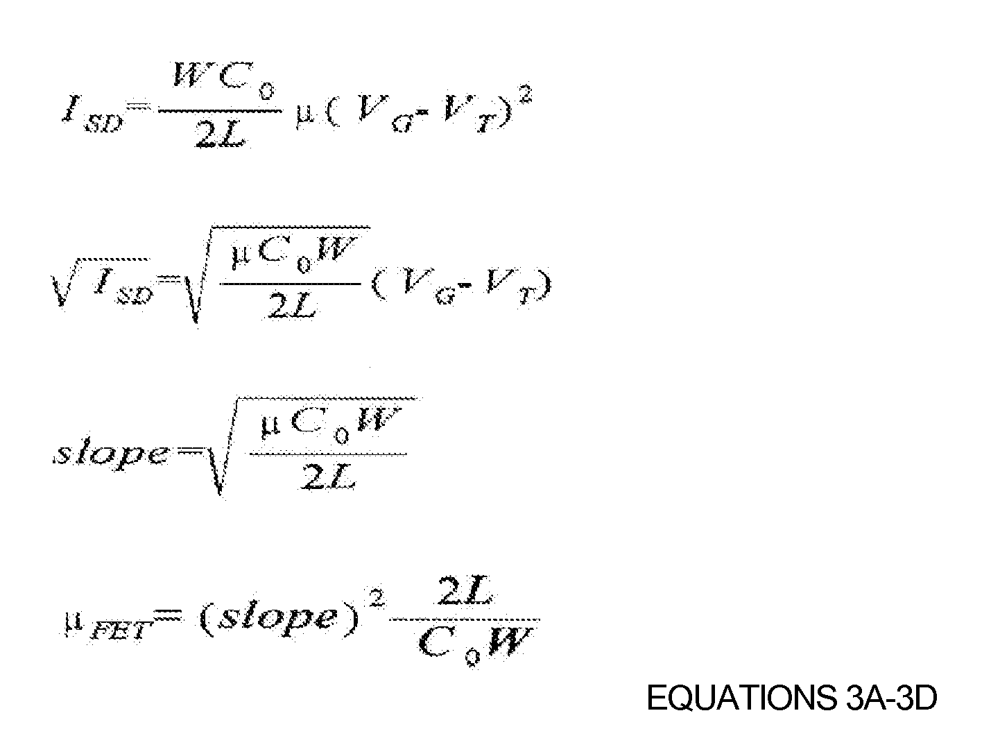
wherein ISD is the source-drain current, µ or µ FET is the charge mobility, Co is the dielectric film capacitance, W is the channel width, L is the channel length, VG is the gate voltage and VT is the threshold voltage. - The on/off current ratio (Ion/Ioff) was taken from the ratio of maximum current in the on-state to minimum current in the off-state. The Ion/Ioff ratio is represented by the following equation:

wherein Ion is the maximum current, Ioff is the off-state leakage current, µ is the charge mobility, σ is the conductivity of the thin film, q is the quantity of electric charge, NA is the density of electric charge, t is the thickness of the semiconductor film, Co is the dielectric film capacitance and VD is the drain voltage.TABLE 1 WATER CONTACT ANGLE CHARGE MOBILITY [CM2/VS] THRESHOLD VOLTAGE ON/OFF CURRENT RATIO Comparative Example 1 55° 1.5x10⁻³ +12V 64.4 Example 1 68° 5.1x10⁻³ +22 V 2.5x10⁴ Example 2 76° 9.1x10⁻³ +4 V 2.1x10⁴ - Referring to Table 1, if the amount of the crosslinking agent increases, the degree of curing increases and the density of the hydroxyl group decreases. As such, the hydrophilic surface of the insulator becomes hydrophobic. In the OTFT according to example embodiments, if the degree of curing of the gate insulating layer increases, then the mobility increases six fold, the on/off current ratio increases and the threshold voltage is approximately 0 V..
- As described above, example embodiments provide an organic insulator composition including a hydroxyl group-containing polymer and a dielectric film and an OTFT using the same. According to example embodiments, the organic insulator composition may be cured at temperatures lower than 130°C. The organic insulator composition according to example embodiments has is more chemically resistance. As such, the organic insulator composition may be used to form a thin film in a low-temperature wet process. As such, the organic insulator composition may be used in the fabrication of a flexible display device.
- The composition according to example embodiments may impart increased electrical properties if used in the fabrication of an OTFT. If a curing process is performed, the organic insulator composition may prevent (or reduce) the formation of reaction by-products, increasing the electrical properties.
- The foregoing is illustrative of example embodiments and is not to be construed as limiting thereof. Although a few example embodiments have been described, those skilled in the art will readily appreciate that many modifications are possible in example embodiments without materially departing from the novel teachings and advantages. Accordingly, all such modifications are intended to be included within the scope of this invention as defined in the claims. In the claims, means-plus-function clauses are intended to cover the structures described herein as performing the recited function, and not only structural equivalents but also equivalent structures. Therefore, it is to be understood that the foregoing is illustrative of various example embodiments and is not to be construed as limited to the specific embodiments disclosed, and that modifications to the disclosed embodiments, as well as other embodiments, are intended to be included within the scope of the appended claims.
Claims (15)
- An organic insulator composition, comprising a hydroxyl group-containing oligomer or hydroxyl group-containing polymer; and a crosslinking agent.
- The organic insulator composition as set forth in claim 1, wherein the hydroxyl group-containing polymer is selected from a group consisting of polyvinylalcohol, polyvinylphenol, poly(hydroxyphenylmaleimide-co-hydroxystyrene), polyhydroxyimide, poly(vinylalcohol-co-ethylene) and copolymers thereof.
- The organic insulator composition as set forth in claim 1, wherein the hydroxyl group-containing oligomer or hydroxyl group-containing polymer is selected from a group consisting of oligomers or polymers represented by Formula (1) to (3) below:


- The organic insulator composition as set forth in claim 3, wherein X of Formula (1) is selected from a group consisting of


- The organic insulator composition as set forth in claim 3 or 4, wherein Yof Formula (1) is selected from a group consisting of


- The organic insulator composition as set forth in claim 3, 4 or 5 wherein Z of Formula (1) is selected from a group consisting of hydrogen (H),

- The organic insulator composition as set forth in claim 3, wherein the hydroxyl group-containing oligomer or hydroxyl group-containing polymer is selected from a group consisting of oligomers or polymers represented by Formulas (4) to (10) below:


- The organic insulator composition as set forth in any of claims 1-7, wherein the crosslinking agent is a compound having at least two vinyl ether groups.
- The organic insulator composition as set forth in claim 8, wherein the crosslinking agent is selected from a group consisting of 2,2'-bis(4-(2-(vinyloxy)ethoxy)phenyl)propane (BPA-DEVE), 1,1,1-tris(4-(2-(vinyloxy)ethoxy]phenyl)ethane, 1,3,5-tris(2-(vinyloxy)ethoxy)benzene, poly(ethylene glycol)divinyl ether, 4,4'-bis-but-3-enyloxy-biphenyl, 1,5-bis-but-3-enyloxy-naphthalene and mixtures thereof.
- The organic insulator composition as set forth in any of claims 1-9, wherein the crosslinking agent is used in an amount ranging from a minimum value of Equation (1) to a maximum value of Equation (2) based on an amount of the hydroxyl group-containing oligomer or hydroxyl group-containing polymer:


- A dielectric film, comprising a compound including the organic insulator composition according to any of claims 1-10, wherein the crosslinking agent has at least two vinyl ether groups and the hydroxyl group-containing oligomers or hydroxyl group-containing polymers are crosslinked using the crosslinking agent.
- The dielectric film as set forth in claim 11, wherein the compound of the dielectric film is a compound represented by Formula (11):

- The dielectric film as set forth in claim 12, wherein X of Formula (11) is selected from a group consisting of


Yof Formula (11) is selected from a group consisting of


- An organic thin film transistor, comprising a gate electrode on a substrate; a gate insulating layer on the gate electrode; source and drain electrodes on the gate insulating layer; and an organic semiconductor layer contacting the gate insulating layer, wherein the gate insulating layer includes the dielectric film according to any of claims 11-13.
- An electronic device comprising a plurality of thin film transistors according to claim 14.
Priority Applications (1)
| Application Number | Priority Date | Filing Date | Title |
|---|---|---|---|
| EP12197845.6A EP2575188B1 (en) | 2007-05-19 | 2008-05-08 | Organic insulator composition including a hydroxyl group-containing polymer, dielectric film and organic thin film transistor using the same |
Applications Claiming Priority (1)
| Application Number | Priority Date | Filing Date | Title |
|---|---|---|---|
| KR1020070048930A KR101364275B1 (en) | 2007-05-19 | 2007-05-19 | Insulator Composition Comprising Hydroxy group-containing Polymer and Dielectric Film and Organic Thin Film Transistor Using the Same |
Related Child Applications (1)
| Application Number | Title | Priority Date | Filing Date |
|---|---|---|---|
| EP12197845.6A Division EP2575188B1 (en) | 2007-05-19 | 2008-05-08 | Organic insulator composition including a hydroxyl group-containing polymer, dielectric film and organic thin film transistor using the same |
Publications (2)
| Publication Number | Publication Date |
|---|---|
| EP1995799A2 true EP1995799A2 (en) | 2008-11-26 |
| EP1995799A3 EP1995799A3 (en) | 2010-10-06 |
Family
ID=39672709
Family Applications (2)
| Application Number | Title | Priority Date | Filing Date |
|---|---|---|---|
| EP08155916A Withdrawn EP1995799A3 (en) | 2007-05-19 | 2008-05-08 | Organic insulator composition including a hydroxyl group-containing polymer, dielectric film and organic thin film transistor using the same |
| EP12197845.6A Not-in-force EP2575188B1 (en) | 2007-05-19 | 2008-05-08 | Organic insulator composition including a hydroxyl group-containing polymer, dielectric film and organic thin film transistor using the same |
Family Applications After (1)
| Application Number | Title | Priority Date | Filing Date |
|---|---|---|---|
| EP12197845.6A Not-in-force EP2575188B1 (en) | 2007-05-19 | 2008-05-08 | Organic insulator composition including a hydroxyl group-containing polymer, dielectric film and organic thin film transistor using the same |
Country Status (3)
| Country | Link |
|---|---|
| US (1) | US8003729B2 (en) |
| EP (2) | EP1995799A3 (en) |
| KR (1) | KR101364275B1 (en) |
Cited By (3)
| Publication number | Priority date | Publication date | Assignee | Title |
|---|---|---|---|---|
| EP2524947A1 (en) * | 2011-05-19 | 2012-11-21 | Samsung Electronics Co., Ltd. | Organic passivation layer composition, transistor and/or electronic device including organic passivation layer fabricated therefrom |
| TWI418073B (en) * | 2010-03-18 | 2013-12-01 | Nat Univ Tsing Hua | Electronic grade silk solution, otft with silk protein as dielectric material and methods for manufacturing the same |
| TWI418072B (en) * | 2010-05-28 | 2013-12-01 | Nat Univ Tsing Hua | Otft using paper as substrate and silk protein as dielectric material and method for manufacturing the same |
Families Citing this family (13)
| Publication number | Priority date | Publication date | Assignee | Title |
|---|---|---|---|---|
| CN102981368B (en) * | 2004-05-14 | 2015-03-04 | 日产化学工业株式会社 | Antireflective film-forming composition containing vinyl ether compound |
| EP2277944A3 (en) * | 2009-07-24 | 2012-01-04 | Electronics and Telecommunications Research Institute | Composition for organic dielectric and organic thin film transistor formed using the same |
| US8164089B2 (en) * | 2009-10-08 | 2012-04-24 | Xerox Corporation | Electronic device |
| JP5656049B2 (en) * | 2010-05-26 | 2015-01-21 | ソニー株式会社 | Thin film transistor manufacturing method |
| US8692238B2 (en) | 2012-04-25 | 2014-04-08 | Eastman Kodak Company | Semiconductor devices and methods of preparation |
| US8779415B2 (en) | 2012-11-08 | 2014-07-15 | Eastman Kodak Company | Devices containing organic polymeric multi-metallic composites |
| CN106688050B (en) | 2014-06-11 | 2018-09-18 | 伊斯曼柯达公司 | The device of dielectric layer with band polymer containing thiosulfate |
| US9637581B2 (en) | 2014-06-11 | 2017-05-02 | Eastman Kodak Company | Thiosulfate-containing polymers associated with photosensitizer component |
| US9453095B2 (en) | 2014-06-11 | 2016-09-27 | Eastman Kodak Company | Photocurable and thermally curable thiosulfate-containing polymers |
| US9653694B2 (en) | 2014-06-11 | 2017-05-16 | Eastman Kodak Company | Precursor dielectric composition with thiosulfate-containing polymers |
| US9691997B2 (en) | 2014-06-11 | 2017-06-27 | Eastman Kodak Company | Devices having dielectric layers with thiosulfate-containing polymers |
| US10026911B2 (en) | 2016-01-15 | 2018-07-17 | Corning Incorporated | Structure for transistor switching speed improvement utilizing polar elastomers |
| KR101927372B1 (en) * | 2017-04-19 | 2019-03-12 | 한국과학기술원 | Method of Preparing Polymer Insulator Film for Thin-Film Transistor |
Citations (3)
| Publication number | Priority date | Publication date | Assignee | Title |
|---|---|---|---|---|
| EP0405946A2 (en) * | 1989-06-30 | 1991-01-02 | New Oji Paper Co., Ltd. | Method for producing a heat-sensitive recording material |
| US6121218A (en) * | 1997-11-12 | 2000-09-19 | Thompson; Andrew Michael | Priming composition for bonding photoresists on substrates |
| WO2001033649A1 (en) | 1999-11-02 | 2001-05-10 | Koninklijke Philips Electronics N.V. | Method of producing vertical interconnects between thin film microelectronic devices and products comprising such vertical interconnects |
Family Cites Families (3)
| Publication number | Priority date | Publication date | Assignee | Title |
|---|---|---|---|---|
| US20050279995A1 (en) | 2004-06-21 | 2005-12-22 | Samsung Electronics Co., Ltd. | Composition for preparing organic insulating film and organic insulating film prepared from the same |
| US20090092814A1 (en) * | 2006-04-21 | 2009-04-09 | Toyoki Kunitake | Method for Manufacturing Polymer Thin Film and Polymer Thin Film |
| KR101224723B1 (en) * | 2006-09-15 | 2013-01-21 | 삼성전자주식회사 | Composition for Preparing Organic Insulating Film and Organic Insulating Layer and Organic Thin Film Transistor Prepared by Using the Same |
-
2007
- 2007-05-19 KR KR1020070048930A patent/KR101364275B1/en active IP Right Grant
-
2008
- 2008-04-16 US US12/081,452 patent/US8003729B2/en not_active Expired - Fee Related
- 2008-05-08 EP EP08155916A patent/EP1995799A3/en not_active Withdrawn
- 2008-05-08 EP EP12197845.6A patent/EP2575188B1/en not_active Not-in-force
Patent Citations (3)
| Publication number | Priority date | Publication date | Assignee | Title |
|---|---|---|---|---|
| EP0405946A2 (en) * | 1989-06-30 | 1991-01-02 | New Oji Paper Co., Ltd. | Method for producing a heat-sensitive recording material |
| US6121218A (en) * | 1997-11-12 | 2000-09-19 | Thompson; Andrew Michael | Priming composition for bonding photoresists on substrates |
| WO2001033649A1 (en) | 1999-11-02 | 2001-05-10 | Koninklijke Philips Electronics N.V. | Method of producing vertical interconnects between thin film microelectronic devices and products comprising such vertical interconnects |
Non-Patent Citations (1)
| Title |
|---|
| JANOS VERES ET AL: "Gate Insulators in Organic Field-Effect Transistors", CHEMISTRY OF MATERIALS, vol. 16, no. 23, 11 September 2004 (2004-09-11), pages 4543 - 4555, XP055028537, ISSN: 0897-4756, DOI: 10.1021/cm049598q * |
Cited By (6)
| Publication number | Priority date | Publication date | Assignee | Title |
|---|---|---|---|---|
| TWI418073B (en) * | 2010-03-18 | 2013-12-01 | Nat Univ Tsing Hua | Electronic grade silk solution, otft with silk protein as dielectric material and methods for manufacturing the same |
| TWI418072B (en) * | 2010-05-28 | 2013-12-01 | Nat Univ Tsing Hua | Otft using paper as substrate and silk protein as dielectric material and method for manufacturing the same |
| EP2524947A1 (en) * | 2011-05-19 | 2012-11-21 | Samsung Electronics Co., Ltd. | Organic passivation layer composition, transistor and/or electronic device including organic passivation layer fabricated therefrom |
| CN102786825A (en) * | 2011-05-19 | 2012-11-21 | 三星电子株式会社 | Organic passivation layer composition, transistor and/or electronic device including organic passivation layer fabricated therefrom |
| JP2012244181A (en) * | 2011-05-19 | 2012-12-10 | Samsung Electronics Co Ltd | Organic protective film composition, thin film transistor including organic protective film manufactured from the same, and electronic element |
| US9023980B2 (en) | 2011-05-19 | 2015-05-05 | Samsung Electronics Co., Ltd. | Organic passivation layer composition, transistor and/or electronic device including organic passivation layer fabricated therefrom |
Also Published As
| Publication number | Publication date |
|---|---|
| US20080283829A1 (en) | 2008-11-20 |
| EP2575188A3 (en) | 2013-04-17 |
| EP2575188A2 (en) | 2013-04-03 |
| EP2575188B1 (en) | 2014-05-21 |
| US8003729B2 (en) | 2011-08-23 |
| EP1995799A3 (en) | 2010-10-06 |
| KR101364275B1 (en) | 2014-02-18 |
| KR20080102109A (en) | 2008-11-24 |
Similar Documents
| Publication | Publication Date | Title |
|---|---|---|
| EP2575188B1 (en) | Organic insulator composition including a hydroxyl group-containing polymer, dielectric film and organic thin film transistor using the same | |
| EP1679754B1 (en) | Organic thin film transistor including fluorine-based polymer thin film | |
| KR101379616B1 (en) | Organic Thin Film Transistor with improved Interface Characteristics and Method of Preparing the Same | |
| US9537102B2 (en) | Fused polycyclic heteroaromatic compound, organic thin film including compound and electronic device including organic thin film | |
| US7750342B2 (en) | Insulating organic polymer, organic insulating layer formed using the insulating polymer, and organic thin film transistor comprising the insulating layer | |
| US7923718B2 (en) | Organic thin film transistor with dual layer electrodes | |
| KR101130404B1 (en) | Organic Insulator Composition Comprising High Dielectric Constant Insulator Dispersed in Hyperbranched Polymer and Organic Thin Film Transistor Using the Same | |
| EP2014722A1 (en) | Composition and Organic Insulator Prepared Using the Same | |
| US7675059B2 (en) | Copolymer, organic insulating layer composition, and organic insulating layer and organic thin film transistor manufactured using the same | |
| US9853226B2 (en) | Fused polycyclic heteroaromatic compound, organic thin film including compound and electronic device including organic thin film | |
| US10312375B2 (en) | Thin-film transistor, method for producing thin-film transistor and image display apparatus using thin-film transistor | |
| US8742410B2 (en) | Fused polycyclic heteroaromatic compound, organic thin film including the compound and electronic device including the organic thin film | |
| KR20100055410A (en) | Process for producing organic semiconductor element, organic semiconductor element, and organic semiconductor device | |
| US20070194305A1 (en) | Organic thin film transistor comprising fluorine-based polymer thin film and method for fabricating the same | |
| KR20080047542A (en) | Transistor, method for manufacturing same, and semiconductor device comprising such transistor | |
| US7928181B2 (en) | Semiconducting polymers | |
| KR100889020B1 (en) | Thin-film transistors utilizing multiple stacked layers acting as a gate insulator | |
| CA2675081C (en) | Electronic device comprising semiconducting polymers | |
| US20130137848A1 (en) | Organic semiconductor compound, organic thin film including the organic semiconductor compound and electronic device including the organic thin film, and method of manufacturing the organic thin film | |
| EP2063471B1 (en) | Organic field effect transistor | |
| JP5254540B2 (en) | Transistor, organic semiconductor device, and manufacturing method thereof |
Legal Events
| Date | Code | Title | Description |
|---|---|---|---|
| PUAI | Public reference made under article 153(3) epc to a published international application that has entered the european phase |
Free format text: ORIGINAL CODE: 0009012 |
|
| AK | Designated contracting states |
Kind code of ref document: A2 Designated state(s): AT BE BG CH CY CZ DE DK EE ES FI FR GB GR HR HU IE IS IT LI LT LU LV MC MT NL NO PL PT RO SE SI SK TR |
|
| AX | Request for extension of the european patent |
Extension state: AL BA MK RS |
|
| PUAL | Search report despatched |
Free format text: ORIGINAL CODE: 0009013 |
|
| AK | Designated contracting states |
Kind code of ref document: A3 Designated state(s): AT BE BG CH CY CZ DE DK EE ES FI FR GB GR HR HU IE IS IT LI LT LU LV MC MT NL NO PL PT RO SE SI SK TR |
|
| AX | Request for extension of the european patent |
Extension state: AL BA MK RS |
|
| 17P | Request for examination filed |
Effective date: 20110330 |
|
| AKX | Designation fees paid |
Designated state(s): FR GB NL |
|
| REG | Reference to a national code |
Ref country code: DE Ref legal event code: R108 Effective date: 20110526 |
|
| 17Q | First examination report despatched |
Effective date: 20120620 |
|
| RAP1 | Party data changed (applicant data changed or rights of an application transferred) |
Owner name: SAMSUNG ELECTRONICS CO., LTD. |
|
| STAA | Information on the status of an ep patent application or granted ep patent |
Free format text: STATUS: THE APPLICATION IS DEEMED TO BE WITHDRAWN |
|
| 18D | Application deemed to be withdrawn |
Effective date: 20130103 |